JP2007517477A - Replica bias voltage regulator - Google Patents
Replica bias voltage regulator Download PDFInfo
- Publication number
- JP2007517477A JP2007517477A JP2006547515A JP2006547515A JP2007517477A JP 2007517477 A JP2007517477 A JP 2007517477A JP 2006547515 A JP2006547515 A JP 2006547515A JP 2006547515 A JP2006547515 A JP 2006547515A JP 2007517477 A JP2007517477 A JP 2007517477A
- Authority
- JP
- Japan
- Prior art keywords
- voltage
- replica
- leg
- output
- current
- Prior art date
- Legal status (The legal status is an assumption and is not a legal conclusion. Google has not performed a legal analysis and makes no representation as to the accuracy of the status listed.)
- Pending
Links
- 230000004044 response Effects 0.000 claims abstract description 26
- 230000033228 biological regulation Effects 0.000 claims abstract description 17
- 230000014759 maintenance of location Effects 0.000 claims description 2
- 230000003321 amplification Effects 0.000 claims 1
- 238000003199 nucleic acid amplification method Methods 0.000 claims 1
- 239000003990 capacitor Substances 0.000 description 7
- 230000007423 decrease Effects 0.000 description 7
- 230000001052 transient effect Effects 0.000 description 6
- 238000010586 diagram Methods 0.000 description 5
- 230000003068 static effect Effects 0.000 description 3
- 238000004088 simulation Methods 0.000 description 2
- 230000000052 comparative effect Effects 0.000 description 1
- 230000008878 coupling Effects 0.000 description 1
- 238000010168 coupling process Methods 0.000 description 1
- 238000005859 coupling reaction Methods 0.000 description 1
- 230000003247 decreasing effect Effects 0.000 description 1
- 230000001934 delay Effects 0.000 description 1
- 230000000694 effects Effects 0.000 description 1
- 238000005516 engineering process Methods 0.000 description 1
- 238000004519 manufacturing process Methods 0.000 description 1
- 230000007246 mechanism Effects 0.000 description 1
- 230000001105 regulatory effect Effects 0.000 description 1
- 238000012358 sourcing Methods 0.000 description 1
- 230000007704 transition Effects 0.000 description 1
Images


Classifications
-
- G—PHYSICS
- G05—CONTROLLING; REGULATING
- G05F—SYSTEMS FOR REGULATING ELECTRIC OR MAGNETIC VARIABLES
- G05F1/00—Automatic systems in which deviations of an electric quantity from one or more predetermined values are detected at the output of the system and fed back to a device within the system to restore the detected quantity to its predetermined value or values, i.e. retroactive systems
- G05F1/10—Regulating voltage or current
- G05F1/46—Regulating voltage or current wherein the variable actually regulated by the final control device is dc
- G05F1/56—Regulating voltage or current wherein the variable actually regulated by the final control device is dc using semiconductor devices in series with the load as final control devices
- G05F1/575—Regulating voltage or current wherein the variable actually regulated by the final control device is dc using semiconductor devices in series with the load as final control devices characterised by the feedback circuit
Abstract
レプリカバイアス電圧調整回路(100)が局部的な正のフィードバックを介して高周波数応答を与え、かつ負のフィードバックループを介して低周波数応答を与える。電圧調整回路(100)の電流コンベアー器(106)は出力電圧(Vload)をしてレプリカ電圧(Vrep)に実質的に従わせる。演算増幅器(102)が基準電圧(Vrep)とレプリカ電圧(Vrep)との比較に基づいて電流コンベアー器(104)に供給される電流を制御することにより負のフィードバックが与えられる。 A replica bias voltage adjustment circuit (100) provides a high frequency response through local positive feedback and a low frequency response through a negative feedback loop. The current conveyor unit (106) of the voltage regulation circuit (100) causes the output voltage (Vload) to substantially follow the replica voltage (Vrep). Negative feedback is provided by the operational amplifier (102) controlling the current supplied to the current conveyor (104) based on a comparison of the reference voltage (Vrep) and the replica voltage (Vrep).
Description
この発明は電圧調整回路に関するものであり、特にレプリカバイアス電圧調整回路に関するものである。 The present invention relates to a voltage adjustment circuit, and more particularly to a replica bias voltage adjustment circuit.
集積回路素子において電圧調整回路は種々の多くの目的に応えることができる。特に挙げられるのは集積回路素子のある部分のための調整内部電力供給電圧としての使用である。多くの応用の内のふたつとして電圧調整器は電力供給電圧をダイナミックランダムアクセスメモリー(DRAM)やスタティックRAM(SRAM)などのメモリー素子内のメモリーセルアレイに供給することができる。 In an integrated circuit element, the voltage regulator circuit can meet many different purposes. Particularly mentioned is its use as a regulated internal power supply voltage for certain parts of an integrated circuit element. As two of many applications, the voltage regulator can supply a power supply voltage to a memory cell array in a memory device such as a dynamic random access memory (DRAM) or a static RAM (SRAM).
種々のタイプの電圧調整器中にレプリカバイアス電圧調整器がある。一般に、レプリカバイアス電圧調整器中では回路の一部(例えばレッグ)に生成された電圧はより大きなサイズの素子により重複されて負荷(出力)電圧を与える。負荷電圧は重複電圧をなるべく近く追尾することにより調整される。 Among the various types of voltage regulators are replica bias voltage regulators. In general, in a replica bias voltage regulator, the voltage generated in a portion of the circuit (eg, leg) is duplicated by a larger size element to provide a load (output) voltage. The load voltage is adjusted by tracking the overlapping voltage as close as possible.
従来のレプリカバイアス電圧調整器は基本的にはアクティブ(動的)ライン調整とパッシブ(静的)負荷調整を使っている。そのような試みは少ないDC負荷調整のコストで良好な高周波数過渡現象応答を達成することができる。 Conventional replica bias voltage regulators basically use active (dynamic) line regulation and passive (static) load regulation. Such an attempt can achieve a good high frequency transient response at low DC load regulation costs.
DC負荷調整を改善してオーバーシュートを防止すべく、永久または切換えダミー負荷が提案されてきた。現存のレプリカバイアス電圧調整器はアクティブ(動的)ライン調整とパッシブ(静的)負荷調整とを持っている。負荷電流範囲に亙って制御出力電圧を良くするべく種々の改善が提案されてきた。迅速電圧比較器の使用がそれに含まれるものであって、ダミー負荷または追加の電流ソーシング要素をスイッチオン/オフしている。 Permanent or switched dummy loads have been proposed to improve DC load regulation and prevent overshoot. Existing replica bias voltage regulators have active (dynamic) line regulation and passive (static) load regulation. Various improvements have been proposed to improve the control output voltage over the load current range. It includes the use of a quick voltage comparator, which switches on / off dummy loads or additional current sourcing elements.
スイッチ切換えダミー負荷を使った試みの一例を図11に示す。これは従来のレプリカバイアス電圧調整回路1100であってダミー負荷(Rdummy)を有しており、該負荷は出力電圧(Vpwr)が基準電圧(Vref)を超えたときに出力経路に切り替わる。逆に出力電圧(Vpwr)が基準電圧(Vref)を下回ったときにはダミー負荷(Rdummy)は出力端から絶縁される。かくしてスイッチ切換えダミー負荷(Rdummy)は出力電圧(Vpwr)を特定の範囲に調整できるのである。
An example of an attempt using a switch switching dummy load is shown in FIG. This is a conventional replica bias
以上に代えて、増加電流負荷条件下でVpwrを低下から防止すべく、スイッチ切換えP−タイプ素子が図12に示すように提案された(アメリカ特許第6,373,231号)。
図12の例では、電圧調整回路1200が、永久ダミー負荷Rdummyに加えて、P−タイプスイッチ切換え素子P1を有している。出力電圧(Vpwr)が基準電圧(Vref)を超えると、該素子P1は切り換えられて負荷素子(Vdummy)に供給される電流を低減し、出力電圧を低減する。逆に、出力電圧(Vpwr)が基準電圧(Vref)を下回ると、素子P1が切り換えられて負荷素子(Vdummy)に供給される電流を増加させ、出力電圧(Vpwr)を上げる。かくしてスイッチ切換え電流供給が出力電圧(Vpwr)を特定の範囲に調整できる。
In the example of FIG. 12, the
上記の従来の構造はいくつかの欠点がある。まず、アクティブ負荷調整(例えば負荷素子のスイッチインまたは電流供給のスイッチオン)は比例的応答でも時間的に連続したものでもない。つまり、負荷調整が全ての時間に起きるのではなくて、負荷電流が極端に低いかまたは極端に高い期間の間だけ調整が起きるのである。電圧比較器(Comp)が使われるので、与えられた調整は「勝者が全てを一人占めする」タイプの調整であり、負荷電流変動と補償電流との間の比例性を持つのではないのである。 The conventional structure described above has several drawbacks. First, active load regulation (eg, load element switch-in or current supply switch-on) is neither proportional response nor continuous in time. That is, load adjustment does not occur all the time, but only during periods when the load current is extremely low or extremely high. Since a voltage comparator (Comp) is used, the given adjustment is a “winner occupies all” type adjustment and not a proportionality between the load current variation and the compensation current.
第2に、従来のスイッチ負荷調整は応答において好ましくない遅れを有している。迅速な比較器が用いられたとしても、電流技術は1〜2ナノ秒より早い応答を保証できないのである。応用分野(例えばファースト(fast)RAM)のいかんによってはこれでは不充分である。つまり負荷調整メカニズムは高周波数ドメイン(10MHz〜GHz)では良く作動しないのである。何故なら迅速な電圧比較器が駆動されているフィードバックループでさえも応答時間は数ナノ秒のオーダーだからである。 Second, conventional switch load regulation has an undesirable delay in response. Even if a quick comparator is used, current technology cannot guarantee a response faster than 1-2 nanoseconds. Depending on the field of application (eg fast RAM) this is not sufficient. That is, the load adjustment mechanism does not work well in the high frequency domain (10 MHz to GHz). This is because the response time is on the order of a few nanoseconds even in a feedback loop in which a rapid voltage comparator is driven.
第3に、上記の構造は余分な電圧比較器を揃える必要がある。これは動作電流の消費を増加させることになる。 Third, the above structure requires an extra voltage comparator. This increases the consumption of operating current.
上記に鑑みて、上記した従来の試みに見られる欠点のない電圧調整器を得ることが望まれる。特に高低の両周波数ドメインでアクティブ(動的)負荷調整と低減された出力インピーダンスを有したレプリカバイアス電圧調整器が望まれるのである。 In view of the above, it would be desirable to obtain a voltage regulator that is free from the drawbacks found in the prior attempts described above. In particular, a replica bias voltage regulator with active load regulation and reduced output impedance in both high and low frequency domains is desired.
この発明は負のフィードバックループを有した電圧調整回路を含むものであって、該フィードバックループはレプリカ電圧と所定の基準電圧との間の比較に応じて供給電流を変更する。加えて、電流コンベアー回路がレプリカノードと出力ノードとに接続されて出力電圧を与える。電流コンベアー回路はレプリカ電圧と出力電圧とを相互に反映させる。 The present invention includes a voltage regulation circuit having a negative feedback loop that changes the supply current in response to a comparison between the replica voltage and a predetermined reference voltage. In addition, a current conveyor circuit is connected to the replica node and the output node to provide an output voltage. The current conveyor circuit reflects the replica voltage and the output voltage to each other.
またこの発明は電流コンベアー回路を具えた電圧調整回路を含むものであり、電流コンベアー回路が有するレプリカレッグはレプリカ電圧と出力レッグとを与えるものであり、調整出力電圧を与えるレプリカレッグと並列に配列されている。レプリカレッグと出力レッグとはクロス結合アクティブ素子を有しており、該素子が提供する迅速な正のフィードバックはレプリカ電圧と出力電圧とを相互に追尾させるものである。電圧調整回路はさらに少なくとも1個の負荷供給トランジスターを有しており、該トランジスターは出力レッグと並列に配列されていて、出力レッグの電流に従う出力ノードに電流を供給する。 In addition, the present invention includes a voltage adjustment circuit including a current conveyor circuit, and a replica leg included in the current conveyor circuit provides a replica voltage and an output leg, and is arranged in parallel with a replica leg that provides an adjustment output voltage. Has been. The replica leg and the output leg have cross-coupled active elements, and the rapid positive feedback provided by the elements tracks the replica voltage and the output voltage with each other. The voltage regulator circuit further includes at least one load supply transistor, which is arranged in parallel with the output leg and supplies current to the output node according to the current of the output leg.
さらにこの発明は電圧調整回路を含むものであって、該回路の負のフィードバックループはレプリカ電圧と基準電圧との差に応じてレプリカ電圧ノードに供給される電流を変更して、レプリカ電圧の低周波数調整を与えるものである。加えて、電圧調整回路は電流コンベアー回路を有しており、該電流コンベアー回路の電圧反映回路は出力電圧をレプリカ電圧に従わせて、出力電圧の高周波数調整を与えるものである。 Further, the present invention includes a voltage adjustment circuit, and the negative feedback loop of the circuit changes the current supplied to the replica voltage node according to the difference between the replica voltage and the reference voltage, thereby reducing the replica voltage. Gives frequency adjustment. In addition, the voltage adjustment circuit has a current conveyor circuit, and the voltage reflection circuit of the current conveyor circuit gives high frequency adjustment of the output voltage by making the output voltage follow the replica voltage.
この発明を実施するモード。図示のレプリカバイアス電圧調整器は連続比例負荷調整を与えるものであり、上記した従来の例に比べて秀れた高周波数負荷過渡現象に対する疑似即時応答を与えるものである。 Mode for carrying out this invention. The replica bias voltage regulator shown provides continuous proportional load regulation and provides a pseudo-immediate response to high frequency load transients superior to the prior art described above.
レプリカバイアス電圧調整器100は増幅器102と、供給部分104と、電流コンベアー器106と、レプリカ負荷108と、補助負荷供給部分110と、負荷112とを有している。レプリカ電圧(Vrep)はあるノードVnet5において発生され、出力電圧(Vload)はノードVnet6において発生される。
The replica
増幅器102は演算増幅器であって、下記のように負のフィードバックループにおいて動作するものである。増幅器102の非反転入力端は基準電圧(Vref)を受け、反転入力端はレプリカ電圧(Vrep)を受ける。 The amplifier 102 is an operational amplifier and operates in a negative feedback loop as described below. The non-inverting input terminal of the amplifier 102 receives a reference voltage (Vref), and the inverting input terminal receives a replica voltage (Vrep).
供給部分104は電圧調整器100の少なくとも2個の異なるレッグに電流を供給する。出力レッグ(N3/N5)に供給された電流がレプリカレッグ(N4/N6)に供給された電流よりも大となるように上記の電流は設定されている。図1に示す例では、供給部分104がn−チャンネルトランジスターN1、N2を有しており、これらのトランジスターは電力供給電圧Vccに接続されたドレインと増幅器102の出力端に共通に接続されたゲートとを有している。
トランジスターN1はトランジスターN2より「n」倍大きくなるように設定されている。つまりトランジスターN1:N2のサイズ比はn:1であり、nは1より大である。トランジスターN2はレプリカレッグに電流を供給し、トランジスターN1は出力レッグおよび補助負荷素子110に電流を供給する。 The transistor N1 is set to be “n” times larger than the transistor N2. That is, the size ratio of the transistors N1: N2 is n: 1, where n is greater than 1. Transistor N2 supplies current to the replica leg, and transistor N1 supplies current to the output leg and auxiliary load element 110.
電流コンベアー回路106はレプリカレッグ上にレプリカ電圧(Vrep)を供給し、出力レッグ上に出力電圧(Vload)を供給する。しかし従来の構造とは異なり、それらの回路レッグは「電圧ミラー」として配列されており、レプリカ電圧(Vrep)は実質的には出力電圧(Vload)を追尾するようにされ、その逆も真である。 The current conveyor circuit 106 supplies a replica voltage (Vrep) on the replica leg and an output voltage (Vload) on the output leg. However, unlike the conventional structure, their circuit legs are arranged as “voltage mirrors”, and the replica voltage (Vrep) is effectively made to track the output voltage (Vload), and vice versa. is there.
図1の例では、電流コンベアー器106はn−型トランジスターN4、N6を有しており、これらのトランジスターは互いに直列に配列されてレプリカレッグを構成し、トランジスターN3、N5は直列に配列されて出力レッグを構成する。トランジスターN4のゲートはそのドレインに接続され、トランジスターN6のゲートはトランジスターN5のドレインに接続され、トランジスターN5のゲートはトランジスターN6のドレインに接続されている。かくしてトランジスターN5、N6は相互にクロス結合されている。レプリカ電圧(Vrep)はトランジスターN6のソースに供給され、出力電圧(Vload)はトランジスターN5のソースに供給される。 In the example of FIG. 1, the current conveyor unit 106 includes n-type transistors N4 and N6, which are arranged in series to form a replica leg, and the transistors N3 and N5 are arranged in series. Configure the output leg. The gate of the transistor N4 is connected to the drain thereof, the gate of the transistor N6 is connected to the drain of the transistor N5, and the gate of the transistor N5 is connected to the drain of the transistor N6. Thus, the transistors N5 and N6 are cross-coupled to each other. The replica voltage (Vrep) is supplied to the source of the transistor N6, and the output voltage (Vload) is supplied to the source of the transistor N5.
電流コンベアー器106のトランジスター(N3〜6)は好ましくは整合された素子であり、同じ性質(例えば、しきい値電圧)を有しており、おなじサイズを有している。下記するように、そのような配列によりVrep=Vloadを行なわせる迅速な「正のフィードバック」を与えるものである。 The transistors (N3-6) of the current conveyor device 106 are preferably matched elements, have the same properties (eg, threshold voltage), and have the same size. As described below, such an arrangement provides a quick “positive feedback” that allows Vrep = Vload to be performed.
レプリカレッグ(N4、N6)から供給された電流に応じて、レプリカ負荷108はレプリカ電圧(Vrep)を発生する。レプリカ負荷108は図1において互いに並列な抵抗RrepとコンデンサーCrepにより示されているが、適宜当業者公知の他の形態であってもよい。
The
同様に、レプリカレッグ(N4、N6)から供給された電流に応じて、負荷112は出力電圧(Vload)を発生する。出力負荷112は図1においてコンデンサーCloadと電流負荷(current Iload)を引き出している図示しない負荷抵抗とで表わされている。
Similarly, the
補助負荷供給部分110は出力ノード(Vnet6)に電流を供給し、出力レッグ中の素子に比例したサイズになっている。特にN1:N2についてのサイズ比をn:1とするとN5:N7についてのサイズ比は1:(n−1)となる。 The auxiliary load supply part 110 supplies current to the output node (Vnet6) and is sized in proportion to the elements in the output leg. In particular, if the size ratio for N1: N2 is n: 1, the size ratio for N5: N7 is 1: (n-1).
上記したように、増幅器102はレプリカ電圧(Vrep)に関して負のフィードバックを与える。特に、レプリカ電圧(Vrep)が基準電圧(Vref)より低くなると、増幅器102により供給された出力電圧は増加し、追加の電流がレプリカレッグを通って流れ、レプリカ電圧(Vrep)がより高くなる。逆に、レプリカ電圧(Vrep)が基準電圧(Vref)より上がると、増幅器102により供給される出力電圧は減少して、レプリカレッグを通って流れる電流を低減し、レプリカ電圧(Vrep)が低くなる。 As described above, amplifier 102 provides negative feedback with respect to replica voltage (Vrep). In particular, when the replica voltage (Vrep) becomes lower than the reference voltage (Vref), the output voltage supplied by the amplifier 102 increases, additional current flows through the replica leg, and the replica voltage (Vrep) becomes higher. Conversely, when the replica voltage (Vrep) rises above the reference voltage (Vref), the output voltage supplied by the amplifier 102 decreases, the current flowing through the replica leg decreases, and the replica voltage (Vrep) decreases. .
図1の実施例による電流コンベアー器106の電圧ミラー効果について詳細に以下記載する。素子N3、N4、N5、N6は同じであり、かつ同じDC動作電流であると仮定する。全ての素子N3〜N6は同じ相互コンダクタンス(gm3=gm4=gm5=gm6)を有している。したがって以下の関係が保たれる。

したがって、N3、N4のゲートのノードVnet2への接続の故に、電流コンベアー器106はAC小信号ドメイン中の出力電圧(Vload)をレプリカ電圧(Vrep)に等しくさせ、またその逆も真である。しかし同時に、レプリカ電圧(Vrep)は、増幅器102の実用ゲイン帯域幅内ならば負のフィードバックループにより、またはそれを越えるならばコンデンサーCrepにより、実質的に定常に保たれなければならない。かくして電流コンベアー器106は低出力インピーダンスをレプリカから負荷へと変えるのである。 Thus, because of the connection of the gates of N3, N4 to node Vnet2, the current conveyor 106 makes the output voltage (Vload) in the AC small signal domain equal to the replica voltage (Vrep) and vice versa. At the same time, however, the replica voltage (Vrep) must be kept substantially steady by a negative feedback loop if it is within the practical gain bandwidth of the amplifier 102 or by a capacitor Crep if it is beyond that. Thus, current conveyor 106 changes the low output impedance from replica to load.
回路(例えばIload)の出力容量がレプリカレッグ(N4、N6)中のレプリカ電流より高いと、トランジスターN7は必要ないかなる超過の負荷電流をも横取りする。そのような配列は上記したような(例えば、N1、N2がn:1に設定され、N7、N3〜N6は(n−1):1に設定される)トランジスターのサイズ設定の故に可能なのである。 If the output capacitance of the circuit (eg Iload) is higher than the replica current in the replica legs (N4, N6), transistor N7 will intercept any excess load current required. Such an arrangement is possible due to transistor size settings as described above (eg, N1, N2 are set to n: 1 and N7, N3-N6 are set to (n-1): 1). .
したがって、電流コンベアー器106の動作の故に、出力電圧(Vload)の変動は同様なレプリカ電圧(Vrep)の変動を生み出し、ついで上記したようなライン調整負のフィードバックループによりそれが修正される。観点を変えると、負荷調整は出力電圧(Vload)情報を負のフィードバックループに移すことにより与えられる。かくして、負荷電流(Iload)が増加してVloadが降下すると、ノードVnet3における電圧が降下し、ついでレプリカ電圧(Vrep)が降下する。そのような降下により、ゲートN1、N2のゲート上の電圧を増加させ、ついで出力電圧(Vload)が修正される。 Thus, due to the operation of the current conveyor 106, output voltage (Vload) variations produce similar replica voltage (Vrep) variations, which are then corrected by the line-adjusted negative feedback loop as described above. From another point of view, load regulation is provided by moving the output voltage (Vload) information into a negative feedback loop. Thus, when the load current (Iload) increases and Vload drops, the voltage at the node Vnet3 drops, and then the replica voltage (Vrep) drops. Such a drop increases the voltage on the gates of the gates N1, N2, and then modifies the output voltage (Vload).
図1の実施例による電圧調整回路の応答はより詳細な分析により明らかになろう。下記のような出力インピーダンス等式が得られる。
ここで、gmはトランジスターN3〜N6の相互コンダクタンスであり、a0は増幅器102のゲインであり、ω0は2πf0に等しくてf0は演算増幅器のカットオフ周波数であり、ω1はgm/Crepに等しく、ω2はna0gm/Cloadに等しい。 Here, g m is the transconductance of the transistors N3 to N6, a 0 is the gain of the amplifier 102, ω 0 is equal to 2πf 0 , f 0 is the cutoff frequency of the operational amplifier, and ω 1 is g m 2 / C rep and ω 2 is equal to na 0 g m / C load .
上記の分析に鑑みて出力インピーダンスを最少にするには、広帯域幅電流コンベアートランジスターと演算増幅器(増加a0ω0)および大レプリカ負荷容量(Crep)値(減少ω1)を用いるのが望ましい。約30dBの控え目のDCゲインが広帯域幅演算増幅器には充分である。負荷容量Cloadはそれ自身の極を出力インピーダンス中に導いて、高周波数トランジスター応答を助ける。 In view of the above analysis, it is desirable to use a wide bandwidth current conveyor transistor, an operational amplifier (increase a 0 ω 0 ), and a large replica load capacitance (Crep) value (decrease ω 1 ) to minimize the output impedance. A modest DC gain of about 30 dB is sufficient for a wide bandwidth operational amplifier. The load capacitance Cload guides its own pole into the output impedance and helps the high frequency transistor response.
特別な構成にあっては、増幅器102実用ゲイン帯域幅は55MHzである、ゲインは28dBである。 In a special configuration, the amplifier 102 practical gain bandwidth is 55 MHz and the gain is 28 dB.
図1の実施例において、低および中間周波数ドメインでは、上記のような従来のレプリカバイアス電圧調整器の出力インピーダンスに対して出力インピーダンスはファクターa0低下する。 In the embodiment of FIG. 1, in the low and intermediate frequency domains, the output impedance is reduced by a factor a 0 relative to the output impedance of the conventional replica bias voltage regulator as described above.
ループ単位利得帯域幅(a0ω0)を越えると、出力インピーダンスは降下して、レプリカ分枝コンデンサー(ω1)と負荷コンデンサー(ω2)により導入された極の故にさらに降下する。 Beyond the loop unity gain bandwidth (a 0 ω 0 ), the output impedance drops and falls further due to the pole introduced by the replica branching capacitor (ω 1 ) and the load capacitor (ω 2 ).
したがって、上記したように、Zoutを周波数までできる限り高く最少化するために、大帯域幅演算増幅器(増加a0ω0)と大レプリカ分枝コンデンサー(減少ω1)とを使う必要がある。勿論増加した負荷コンデンサーは迅速電流過渡現象(減少ω2)を扱う上で助けとなる。 Therefore, as described above, it is necessary to use a large bandwidth operational amplifier (increase a 0 ω 0 ) and a large replica branching capacitor (decrease ω 1 ) in order to minimize Zout to the frequency as high as possible. Of course, the increased load capacitor helps in dealing with rapid current transients (decrease ω 2 ).
図1の実施例は図11、12に記したように従来の構造に比べていくつかの利点がある。 The embodiment of FIG. 1 has several advantages over the conventional structure as shown in FIGS.
特に、レプリカバイアス電圧調整器100は第2のフィードバックループを有していない。この結果電流消費が従来の構造よりも小さくなる。これにより典型的に低い電流および/または電力消費素子を必要とする自動車にレプリカバイアス電圧調整器100を応用できるようになる。
In particular, the replica
さらに、レプリカバイアス電圧調整器100は1個の負のフィードバックループのみを有している。これによりループからループへの結合の故に生じる安定性の問題を除くことができる。
Furthermore, the replica
加えて、レプリカバイアス電圧調整器100にあっては、電流コンベアー器中の局地的な正のフィードバックが極端に迅速であり、これにより高周波数過渡現象に対して実質的に瞬間的な応答が可能となる。これは演算増幅器の応答遅れを起こす従来の構造と対照的である。
In addition, in the replica
かくしてこの発明は前記した現存の試みの欠点に対処できるものであり、特に図1の実施例は、追加の増幅器(例えば比較器)を必要としないので、線型負のフィードバックループに与えられる負荷電圧情報による連続および比例負荷調整、良好な高周波数応答、負荷正のフィードバックの動作の良さ、低減された電流消費などを齎すのである。 Thus, the present invention addresses the shortcomings of the existing attempts described above, and in particular, the embodiment of FIG. 1 does not require an additional amplifier (eg, a comparator), so the load voltage applied to the linear negative feedback loop. It takes into account continuous and proportional load regulation by information, good high frequency response, good load positive feedback operation, reduced current consumption, and so on.
表1に結果を示してあり、第1の実施例の負荷調整の態様を示してある。この例は基準電圧が1.300Vに設定されたものである。
表1は図1の例がいかに図2の従来技術のモデルよりも良い調整を提供するかを示している。 Table 1 shows how the example of FIG. 1 provides better adjustment than the prior art model of FIG.
過渡現象をシミュレートするべく、10mAのDC成分と90mAのピーク値を有したパルス電流波形を用いた。下記に詳記するごとく、図1の実施例においては実施例の電圧調整は130mVピーク−ツー−ピークから60mVピーク−ツー−ピークまでの出力降下を生じた。そのような状態を図2の典型的な従来技術の電圧調整器を表すモデルと比較した。 In order to simulate a transient phenomenon, a pulse current waveform having a DC component of 10 mA and a peak value of 90 mA was used. As described in detail below, in the example of FIG. 1, the example voltage regulation resulted in a power drop from 130 mV peak-to-peak to 60 mV peak-to-peak. Such a situation was compared with the model representing the typical prior art voltage regulator of FIG.
図3のタイミング図は過渡現象応答をシミュレートするのに使った負荷電流(Iload)波形を示している。 The timing diagram of FIG. 3 shows the load current (Iload) waveform used to simulate the transient response.
図4のタイミング図は図2の従来技術のケース(OLD CIRCUIT)と図1のそれ(NEW CIRCUIT)についての電力供給応答(Vcc)および出力電圧(Vpwr)とを示している。 The timing diagram of FIG. 4 shows the power supply response (Vcc) and the output voltage (Vpwr) for the prior art case (OLD CIRCUIT) of FIG. 2 and that of FIG. 1 (NEW CIRCUIT).
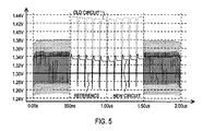
図5は図4のVpwr応答を縦軸(電圧)に沿ってとった断面図であって、入力基準電圧(REFERENCE)をも示しており、図1・2の基準電圧(Vref)に対応するものである。 FIG. 5 is a cross-sectional view of the Vpwr response of FIG. 4 taken along the vertical axis (voltage), and also shows the input reference voltage (REFERENCE), corresponding to the reference voltage (Vref) of FIGS. Is.
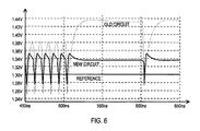
図6は図5のVpwr応答を横軸(時間)に沿ってとった断面図である。図7は図5のVpwr応答を横軸(時間)に沿ってとった断面図と基準電圧入力(Vref)である。図6、7はピーク−ツー−ピークの約130mV(old circuit)から約60mV(new circuit)への電圧の減少を明らかに示している。 FIG. 6 is a cross-sectional view of the Vpwr response of FIG. 5 taken along the horizontal axis (time). FIG. 7 is a cross-sectional view of the Vpwr response of FIG. 5 taken along the horizontal axis (time) and a reference voltage input (Vref). FIGS. 6 and 7 clearly show a decrease in voltage from about 130 mV (old circuit) to about 60 mV (new circuit) of the peak-to-peak.
図8は図3〜7の比較シミュレーションの高周波数過渡現象に因る負荷電圧(Vload)の降下に対する電流コンベアー器106中のノード(Vnet4)の瞬間応答を示している。また図8は出力電圧(Vpwr)をも示している。 FIG. 8 shows the instantaneous response of the node (Vnet4) in the current conveyor 106 to the drop in load voltage (Vload) due to the high frequency transient of the comparative simulation of FIGS. FIG. 8 also shows the output voltage (Vpwr).
図9は周波数ドメインにおける新回路(図1)対旧回路(図2)の出力インピーダンス曲線を示している。高周波数出力インピーダンスの65%の降下が図6、7に示したHF出力リップルの65%降下に正に整合していることが分かる。 FIG. 9 shows the output impedance curve of the new circuit (FIG. 1) versus the old circuit (FIG. 2) in the frequency domain. It can be seen that the 65% drop in high frequency output impedance is positively matched to the 65% drop in HF output ripple shown in FIGS.
図1の実施例においては、電流コンベアー器106の直列結合トランジスターを受容するには、ある電圧「オーバーヘッド」が必要であることが分かる。つまり、トランジスターN2/N1のドレインとトランジスターN5/N6のソースとの間の最小電圧差が必要である。通常のn−チャンネルトランジスターしきい値電圧が大き過ぎた場合には、電流供給部分104(N1、N2)のn−タイプフォロアおいても、または電流コンベアー器N3−N7においても、純粋素子(native device)を使うことにより過剰に必要な電圧オーバーヘッドが補償できる。加えてまたはそれに代えて、N−タイプフォロアのゲートは供給電圧Vccよりも高い電圧を印加することにより「ポンプ」され得る。 In the embodiment of FIG. 1, it can be seen that some voltage “overhead” is required to accept the series coupled transistors of the current conveyor device 106. That is, a minimum voltage difference between the drain of the transistor N2 / N1 and the source of the transistor N5 / N6 is necessary. If the normal n-channel transistor threshold voltage is too high, either in the n-type follower of the current supply portion 104 (N1, N2) or in the current conveyor N3-N7, the pure element (native) By using device, excessive voltage overhead can be compensated. Additionally or alternatively, the gate of the N-type follower can be “pumped” by applying a voltage higher than the supply voltage Vcc.
図1の実施例では電圧調整が改善されるが、応用対象によってはそのような調整は特殊なモードで必要となるだけである。高速度過渡現象応答を不可能とする回路の例を図10に示す。 Although the voltage regulation is improved in the embodiment of FIG. 1, depending on the application, such adjustment is only required in a special mode. An example of a circuit that makes high-speed transient response impossible is shown in FIG.
図10に第2の実施例の電圧調整回路1000を示す。該回路は第1の実施例と同じ構成要素を有しており、各部分は同じ参照文字で示されているが、最初の数字は「1」の代わりに「10」となっている。電流コンベアー器1006はバイパスされており、電圧調整回路1000を現存のもの(図2)から反転させている。pタイプトランジスターP1・2がこの目的に使われている。信号BAYPASSB遷移が低くなると、トランジスターP1・2はオンに切り換わり、電流コンベアー器1006および補助負荷供給1010を短絡させる。
FIG. 10 shows a
かかる構成をとることにより、調整が必要となくなるようなモードで電流消費を低減する。しかし一例では、メモリの応用において、低電力データ保持モードで強い調整は必要でなくなる。 By adopting such a configuration, current consumption is reduced in such a mode that adjustment is not necessary. In one example, however, memory applications do not require strong adjustments in the low power data retention mode.
しかしこの発明は図1の実施例に限定されるものではない。例えば演算増幅器102は2段階回路であってもよい。これにより演算増幅器が最適化される。 However, the present invention is not limited to the embodiment of FIG. For example, the operational amplifier 102 may be a two-stage circuit. This optimizes the operational amplifier.
この発明は電気電子機器製造の分野において広く利用され得るものである。 The present invention can be widely used in the field of manufacturing electrical and electronic equipment.
100: レプリカバイアス電圧調整器
102: 増幅器
106: 電流コンベアー器
108: レプリカ負荷
110: 負荷供給部分
DESCRIPTION OF SYMBOLS 100: Replica bias voltage regulator 102: Amplifier 106: Current conveyor 108: Replica load 110: Load supply part
Claims (20)
第1のn−チャンネルトランジスターがそのドレインに接続されたゲートを有しており、第2のn−チャンネルトランジスターが第1のn−チャンネルトランジスターのソースに接続されたドレインとレプリカノードに接続されたソースとを有しており、出力レッグが第3のn−チャンネルトランジスターと第4のn−チャンネルトランジスターとゲートとソースとを有しており、第3のn−チャンネルトランジスターが第1のn−チャンネルトランジスターのドレインに接続されたゲートを有しており、第4のn−チャンネルトランジスターが第3のn−チャンネルトランジスターのソースに接続されたドレインを有しており、ゲートが第2のn−チャンネルトランジスターのドレインに接続されており、ソースが出力ノードに接続されており、第1〜第4のトランジスターが相互に整合していることを特徴とする請求項3に記載の電圧調整器。 The replica leg has first and second n-channel transistors;
The first n-channel transistor has a gate connected to its drain, and the second n-channel transistor is connected to the drain and the replica node connected to the source of the first n-channel transistor. The output leg has a third n-channel transistor, a fourth n-channel transistor, a gate and a source, and the third n-channel transistor is a first n-channel transistor. The fourth n-channel transistor has a drain connected to the source of the third n-channel transistor, and the gate is a second n- Connected to the drain of the channel transistor, the source is connected to the output node Ri, the voltage regulator of claim 3, the first to fourth transistors are characterized by being aligned with each other.
Applications Claiming Priority (3)
| Application Number | Priority Date | Filing Date | Title |
|---|---|---|---|
| US53191103P | 2003-12-23 | 2003-12-23 | |
| US10/965,445 US7026802B2 (en) | 2003-12-23 | 2004-10-14 | Replica biased voltage regulator |
| PCT/US2004/043756 WO2005062990A2 (en) | 2003-12-23 | 2004-12-22 | Replica biased voltage regulator |
Publications (2)
| Publication Number | Publication Date |
|---|---|
| JP2007517477A true JP2007517477A (en) | 2007-06-28 |
| JP2007517477A5 JP2007517477A5 (en) | 2008-02-07 |
Family
ID=34681660
Family Applications (1)
| Application Number | Title | Priority Date | Filing Date |
|---|---|---|---|
| JP2006547515A Pending JP2007517477A (en) | 2003-12-23 | 2004-12-22 | Replica bias voltage regulator |
Country Status (3)
| Country | Link |
|---|---|
| US (1) | US7026802B2 (en) |
| JP (1) | JP2007517477A (en) |
| WO (1) | WO2005062990A2 (en) |
Families Citing this family (25)
| Publication number | Priority date | Publication date | Assignee | Title |
|---|---|---|---|---|
| US7106042B1 (en) | 2003-12-05 | 2006-09-12 | Cypress Semiconductor Corporation | Replica bias regulator with sense-switched load regulation control |
| CN100399689C (en) * | 2004-04-27 | 2008-07-02 | 株式会社理光 | Switching regulator and method for changing output voltages thereof |
| US7319314B1 (en) * | 2004-12-22 | 2008-01-15 | Cypress Semiconductor Corporation | Replica regulator with continuous output correction |
| US7262586B1 (en) * | 2005-03-31 | 2007-08-28 | Cypress Semiconductor Corporation | Shunt type voltage regulator |
| US7463014B2 (en) * | 2006-02-27 | 2008-12-09 | Avago Technologies General Ip (Singapore) Pte. Ltd. | High impedance current mirror with feedback |
| US7821296B2 (en) * | 2006-08-04 | 2010-10-26 | Analog Devices, Inc. | Stacked buffers |
| US7372748B2 (en) * | 2006-10-16 | 2008-05-13 | Sandisk Corporation | Voltage regulator in a non-volatile memory device |
| US7859240B1 (en) | 2007-05-22 | 2010-12-28 | Cypress Semiconductor Corporation | Circuit and method for preventing reverse current flow into a voltage regulator from an output thereof |
| US7863878B2 (en) * | 2008-08-19 | 2011-01-04 | Oracle America, Inc. | Voltage regulator for write/read assist circuit |
| US20100283445A1 (en) * | 2009-02-18 | 2010-11-11 | Freescale Semiconductor, Inc. | Integrated circuit having low power mode voltage regulator |
| US8319548B2 (en) * | 2009-02-18 | 2012-11-27 | Freescale Semiconductor, Inc. | Integrated circuit having low power mode voltage regulator |
| US8812879B2 (en) * | 2009-12-30 | 2014-08-19 | International Business Machines Corporation | Processor voltage regulation |
| US8400819B2 (en) * | 2010-02-26 | 2013-03-19 | Freescale Semiconductor, Inc. | Integrated circuit having variable memory array power supply voltage |
| US9035629B2 (en) | 2011-04-29 | 2015-05-19 | Freescale Semiconductor, Inc. | Voltage regulator with different inverting gain stages |
| US9143204B2 (en) * | 2011-06-17 | 2015-09-22 | Tensorcom, Inc. | Direct coupled biasing circuit for high frequency applications |
| CN102624232B (en) * | 2012-04-20 | 2014-06-25 | 矽力杰半导体技术(杭州)有限公司 | Precharging circuit and method for DC-DC boost converter |
| US20130328851A1 (en) * | 2012-06-08 | 2013-12-12 | Apple Inc. | Ground noise propagation reduction for an electronic device |
| US9229462B2 (en) | 2013-06-27 | 2016-01-05 | Stmicroelectronics International N.V. | Capless on chip voltage regulator using adaptive bulk bias |
| US9395730B2 (en) * | 2013-06-27 | 2016-07-19 | Stmicroelectronics International N.V. | Voltage regulator |
| CN105684302A (en) * | 2013-11-04 | 2016-06-15 | 马维尔国际贸易有限公司 | Memory effect reduction using low impedance biasing |
| US9831764B2 (en) | 2014-11-20 | 2017-11-28 | Stmicroelectronics International N.V. | Scalable protection voltage generator |
| DE102015205359B4 (en) * | 2015-03-24 | 2018-01-25 | Dialog Semiconductor (Uk) Limited | RESTRAIN LIMIT FOR A LOW DROPOUT CONTROLLER IN A DROPOUT CONDITION |
| EP3435192B1 (en) * | 2017-07-28 | 2022-08-24 | NXP USA, Inc. | Ultra low power linear voltage regulator |
| US11315655B2 (en) | 2020-09-23 | 2022-04-26 | Nxp Usa, Inc. | Low power memory state retention regulator |
| US11616505B1 (en) * | 2022-02-17 | 2023-03-28 | Qualcomm Incorporated | Temperature-compensated low-pass filter |
Citations (4)
| Publication number | Priority date | Publication date | Assignee | Title |
|---|---|---|---|---|
| JPH0236728A (en) * | 1988-05-26 | 1990-02-06 | Philips Gloeilampenfab:Nv | Gain one current limiter |
| JPH08330936A (en) * | 1995-05-31 | 1996-12-13 | Hewlett Packard Co <Hp> | Power supply resistance programming method |
| JPH08328671A (en) * | 1995-05-31 | 1996-12-13 | Sgs Thomson Microelectron Inc | Voltage regulator with stable load pole |
| JPH10187258A (en) * | 1996-12-19 | 1998-07-14 | Texas Instr Inc <Ti> | Drop-out voltage controller |
Family Cites Families (9)
| Publication number | Priority date | Publication date | Assignee | Title |
|---|---|---|---|---|
| US4884161A (en) | 1983-05-26 | 1989-11-28 | Honeywell, Inc. | Integrated circuit voltage regulator with transient protection |
| US4893030A (en) * | 1986-12-04 | 1990-01-09 | Western Digital Corporation | Biasing circuit for generating precise currents in an integrated circuit |
| EP0892332B1 (en) | 1997-07-14 | 2005-03-09 | STMicroelectronics S.r.l. | Low power consumption linear voltage regulator having a fast response with respect to the load transients |
| US6144195A (en) * | 1999-08-20 | 2000-11-07 | Intel Corporation | Compact voltage regulator with high supply noise rejection |
| US6222353B1 (en) | 2000-05-31 | 2001-04-24 | Philips Semiconductors, Inc. | Voltage regulator circuit |
| US6566851B1 (en) * | 2000-08-10 | 2003-05-20 | Applied Micro Circuits, Corporation | Output conductance correction circuit for high compliance short-channel MOS switched current mirror |
| US6373231B1 (en) | 2000-12-05 | 2002-04-16 | Cypress Semiconductor Corp. | Voltage regulator |
| US6522111B2 (en) | 2001-01-26 | 2003-02-18 | Linfinity Microelectronics | Linear voltage regulator using adaptive biasing |
| US6879142B2 (en) * | 2003-08-20 | 2005-04-12 | Broadcom Corporation | Power management unit for use in portable applications |
-
2004
- 2004-10-14 US US10/965,445 patent/US7026802B2/en active Active
- 2004-12-22 WO PCT/US2004/043756 patent/WO2005062990A2/en active Application Filing
- 2004-12-22 JP JP2006547515A patent/JP2007517477A/en active Pending
Patent Citations (4)
| Publication number | Priority date | Publication date | Assignee | Title |
|---|---|---|---|---|
| JPH0236728A (en) * | 1988-05-26 | 1990-02-06 | Philips Gloeilampenfab:Nv | Gain one current limiter |
| JPH08330936A (en) * | 1995-05-31 | 1996-12-13 | Hewlett Packard Co <Hp> | Power supply resistance programming method |
| JPH08328671A (en) * | 1995-05-31 | 1996-12-13 | Sgs Thomson Microelectron Inc | Voltage regulator with stable load pole |
| JPH10187258A (en) * | 1996-12-19 | 1998-07-14 | Texas Instr Inc <Ti> | Drop-out voltage controller |
Also Published As
| Publication number | Publication date |
|---|---|
| US20050134242A1 (en) | 2005-06-23 |
| WO2005062990A2 (en) | 2005-07-14 |
| US7026802B2 (en) | 2006-04-11 |
| WO2005062990A3 (en) | 2005-12-29 |
Similar Documents
| Publication | Publication Date | Title |
|---|---|---|
| JP2007517477A (en) | Replica bias voltage regulator | |
| US10423176B2 (en) | Low-dropout regulators | |
| US10481625B2 (en) | Voltage regulator | |
| KR0182269B1 (en) | A buffer circuit | |
| KR100967261B1 (en) | Voltage regulator | |
| US7982448B1 (en) | Circuit and method for reducing overshoots in adaptively biased voltage regulators | |
| US6653891B1 (en) | Voltage regulation | |
| US7362079B1 (en) | Voltage regulator circuit | |
| Maity et al. | A hybrid-mode operational transconductance amplifier for an adaptively biased low dropout regulator | |
| US10541677B2 (en) | Low output impedance, high speed and high voltage generator for use in driving a capacitive load | |
| US7463014B2 (en) | High impedance current mirror with feedback | |
| JP2007249712A (en) | Linear regulator circuit | |
| KR100924293B1 (en) | Low voltage drop out regulator | |
| Tseng et al. | An integrated linear regulator with fast output voltage transition for dual-supply SRAMs in DVFS systems | |
| Maity et al. | A single-stage low-dropout regulator with a wide dynamic range for generic applications | |
| CN113467559B (en) | Adaptive dynamic zero compensation circuit applied to LDO (low dropout regulator) | |
| KR20060046045A (en) | Constant voltage outputting circuit | |
| US7880452B1 (en) | Trimming circuit and method for replica type voltage regulators | |
| Maity et al. | Dynamic slew enhancement technique for improving transient response in an adaptively biased low-dropout regulator | |
| JP3422706B2 (en) | Startup circuit of reference voltage generator | |
| US9971370B2 (en) | Voltage regulator with regulated-biased current amplifier | |
| CN115840483A (en) | Low dropout regulator with transient enhancement characteristic | |
| US7196505B2 (en) | Device and method for low-power fast-response voltage regulator with improved power supply range | |
| KR20160012858A (en) | Low dropout regulator | |
| JP2006155357A (en) | Voltage lowering circuit |
Legal Events
| Date | Code | Title | Description |
|---|---|---|---|
| A521 | Request for written amendment filed |
Free format text: JAPANESE INTERMEDIATE CODE: A523 Effective date: 20071214 |
|
| A621 | Written request for application examination |
Free format text: JAPANESE INTERMEDIATE CODE: A621 Effective date: 20071217 |
|
| A521 | Request for written amendment filed |
Free format text: JAPANESE INTERMEDIATE CODE: A821 Effective date: 20090629 |
|
| RD02 | Notification of acceptance of power of attorney |
Free format text: JAPANESE INTERMEDIATE CODE: A7422 Effective date: 20090629 |
|
| A977 | Report on retrieval |
Free format text: JAPANESE INTERMEDIATE CODE: A971007 Effective date: 20110112 |
|
| A131 | Notification of reasons for refusal |
Free format text: JAPANESE INTERMEDIATE CODE: A131 Effective date: 20110118 |
|
| A601 | Written request for extension of time |
Free format text: JAPANESE INTERMEDIATE CODE: A601 Effective date: 20110415 |
|
| A602 | Written permission of extension of time |
Free format text: JAPANESE INTERMEDIATE CODE: A602 Effective date: 20110502 |
|
| A601 | Written request for extension of time |
Free format text: JAPANESE INTERMEDIATE CODE: A601 Effective date: 20110517 |
|
| A602 | Written permission of extension of time |
Free format text: JAPANESE INTERMEDIATE CODE: A602 Effective date: 20110601 |
|
| A601 | Written request for extension of time |
Free format text: JAPANESE INTERMEDIATE CODE: A601 Effective date: 20110614 Free format text: JAPANESE INTERMEDIATE CODE: A601 Effective date: 20110614 |
|
| A602 | Written permission of extension of time |
Free format text: JAPANESE INTERMEDIATE CODE: A602 Effective date: 20110623 Free format text: JAPANESE INTERMEDIATE CODE: A602 Effective date: 20110623 |
|
| A02 | Decision of refusal |
Free format text: JAPANESE INTERMEDIATE CODE: A02 Effective date: 20110920 |