JP2007517256A - Scratch resistant light directivity film - Google Patents
Scratch resistant light directivity film Download PDFInfo
- Publication number
- JP2007517256A JP2007517256A JP2006546992A JP2006546992A JP2007517256A JP 2007517256 A JP2007517256 A JP 2007517256A JP 2006546992 A JP2006546992 A JP 2006546992A JP 2006546992 A JP2006546992 A JP 2006546992A JP 2007517256 A JP2007517256 A JP 2007517256A
- Authority
- JP
- Japan
- Prior art keywords
- light
- prism
- prism element
- film
- directing film
- Prior art date
- Legal status (The legal status is an assumption and is not a legal conclusion. Google has not performed a legal analysis and makes no representation as to the accuracy of the status listed.)
- Withdrawn
Links
- 230000003678 scratch resistant effect Effects 0.000 title abstract description 7
- 230000003287 optical effect Effects 0.000 claims description 20
- 230000008878 coupling Effects 0.000 claims description 3
- 238000010168 coupling process Methods 0.000 claims description 3
- 238000005859 coupling reaction Methods 0.000 claims description 3
- 239000000463 material Substances 0.000 description 6
- 230000008859 change Effects 0.000 description 5
- 230000007423 decrease Effects 0.000 description 5
- 238000004519 manufacturing process Methods 0.000 description 3
- 230000009467 reduction Effects 0.000 description 3
- 239000004743 Polypropylene Substances 0.000 description 1
- 239000004793 Polystyrene Substances 0.000 description 1
- 238000003848 UV Light-Curing Methods 0.000 description 1
- 230000005540 biological transmission Effects 0.000 description 1
- 238000007796 conventional method Methods 0.000 description 1
- 238000005520 cutting process Methods 0.000 description 1
- 229910003460 diamond Inorganic materials 0.000 description 1
- 239000010432 diamond Substances 0.000 description 1
- 238000004049 embossing Methods 0.000 description 1
- 238000009434 installation Methods 0.000 description 1
- 239000004973 liquid crystal related substance Substances 0.000 description 1
- 238000000034 method Methods 0.000 description 1
- 229920000058 polyacrylate Polymers 0.000 description 1
- 239000004417 polycarbonate Substances 0.000 description 1
- 229920000515 polycarbonate Polymers 0.000 description 1
- 229920000642 polymer Polymers 0.000 description 1
- -1 polypropylene Polymers 0.000 description 1
- 229920001155 polypropylene Polymers 0.000 description 1
- 229920002223 polystyrene Polymers 0.000 description 1
- 229920002635 polyurethane Polymers 0.000 description 1
- 239000004814 polyurethane Substances 0.000 description 1
- 229920000915 polyvinyl chloride Polymers 0.000 description 1
- 239000004800 polyvinyl chloride Substances 0.000 description 1
- 230000003362 replicative effect Effects 0.000 description 1
- 239000000758 substrate Substances 0.000 description 1
Images


Classifications
-
- G—PHYSICS
- G02—OPTICS
- G02B—OPTICAL ELEMENTS, SYSTEMS OR APPARATUS
- G02B5/00—Optical elements other than lenses
- G02B5/04—Prisms
- G02B5/045—Prism arrays
-
- G—PHYSICS
- G02—OPTICS
- G02B—OPTICAL ELEMENTS, SYSTEMS OR APPARATUS
- G02B5/00—Optical elements other than lenses
- G02B5/02—Diffusing elements; Afocal elements
-
- G—PHYSICS
- G02—OPTICS
- G02B—OPTICAL ELEMENTS, SYSTEMS OR APPARATUS
- G02B5/00—Optical elements other than lenses
- G02B5/04—Prisms
Landscapes
- Physics & Mathematics (AREA)
- General Physics & Mathematics (AREA)
- Optics & Photonics (AREA)
- Optical Elements Other Than Lenses (AREA)
- Planar Illumination Modules (AREA)
Abstract
耐スクラッチ性光指向性フィルムは第1及び第2のプリズム要素を含む構造化表面を有する。第1のプリズム要素は第2のプリズム要素より高く、かつ鈍い先端を有する。第2のプリズム要素はより短く、かつ鋭い先端を有する。得られるフィルムにはオンアクシス光の利得を実質的に犠牲にすることなく、耐スクラッチ性がある。 The scratch resistant light directing film has a structured surface including first and second prism elements. The first prism element is higher than the second prism element and has a blunt tip. The second prism element is shorter and has a sharp tip. The resulting film is scratch resistant without substantially sacrificing on-axis light gain.
Description
本発明は光指向性フィルムに関する。本発明は特に、高さが可変の構造化表面(structured surface)を有する光指向性フィルムに関する。 The present invention relates to a light directing film. In particular, the present invention relates to a light directing film having a structured surface of variable height.
光学ディスプレイを出る光の輝度をディスプレイの表面に対して法線方向、すなわち「オンアクシス(on−axis)」方向に増大させるために、光指向性フィルムが用いられる。光指向性フィルムの1つのタイプは実質的に平坦な表面及び対向する構造化表面を有し、該表面は線形のプリズム要素のアレイを有する。オンアクシス光量を増大させれば、所望量のオンアクシス輝度を生成するのに必要なエネルギーの量が低減される。このことは、ラップトップコンピュータ、計算機、デジタル式腕時計、携帯電話、及び携帯情報端末で使用される光源などの電池式光源を使用する光学ディスプレイにとって特に重要である。 Light directional films are used to increase the brightness of light exiting the optical display in a direction normal to the surface of the display, ie, an “on-axis” direction. One type of light directing film has a substantially flat surface and an opposing structured surface, the surface having an array of linear prism elements. Increasing the amount of on-axis light reduces the amount of energy required to produce the desired amount of on-axis brightness. This is particularly important for optical displays that use battery-powered light sources such as those used in laptop computers, calculators, digital watches, cell phones, and personal digital assistants.
オンアクシス光量をさらに増大させるために、プリズム要素を相互に対して約90℃に交差させた状態で、2枚の光指向性フィルムを相互に近接して設けることが当該技術においては公知である。しかし、この構造を用いた光学ディスプレイは可視的にはっきり分かる明るい点、縞、又は線を呈し得る。この「ウェットアウト(wet−out)」状態は、接触しているか、又は非常に近接して接している隣接するフィルムの表面間の光学的結合によって引き起こされる。この状態を克服するために、プリズム要素がより高く且つより短いプリズム要素のゾーン内に配置されてフィルム間の接触を制限し得る。抗ウェットアウト構造体の代表的な実施形態が、スリーエム社(3M Company)に譲受された米国特許第5,771,328号明細書に記載されている。 In order to further increase the amount of on-axis light, it is known in the art to provide two light directing films close to each other with the prism elements crossing each other at about 90 ° C. . However, optical displays using this structure may exhibit bright spots, stripes, or lines that are clearly visible. This “wet-out” condition is caused by optical coupling between adjacent film surfaces that are in contact or in close contact. To overcome this situation, the prism elements can be placed in the zones of the higher and shorter prism elements to limit contact between the films. An exemplary embodiment of an anti-wetout structure is described in US Pat. No. 5,771,328, assigned to 3M Company.
各プリズム要素の側面は交差して頂点又は頂部を形成する。このプリズム要素の頂点は一般に鋭く、このことはバックライトを出るオンアクシス光量を増大させる際に最も効果的である。しかし、各プリズム要素の上に形成された鋭い頂点は比較的壊れ易く、フィルムに引っかき傷を付け易くする。これは光指向性フィルムが上記のようなデバイスの製造中に取り扱われる際に特に問題であり、フィルムの製造後にプレマスクをフィルムに適用することが必要となる。該プレマスクはフィルムを引っかき傷から保護するが、この後に、光学ディスプレイに設置する前に除去しなければならない。従って、実質的にフィルムの性能を犠牲にすることがない、耐スクラッチ性の光指向性フィルムが必要とされる。 The sides of each prism element intersect to form a vertex or apex. The apex of this prism element is generally sharp, which is most effective in increasing the amount of on-axis light exiting the backlight. However, the sharp vertices formed on each prism element are relatively fragile, making it easier to scratch the film. This is particularly a problem when light-directing films are handled during the manufacture of devices as described above, and it is necessary to apply a premask to the film after the film is manufactured. The pre-mask protects the film from scratches, but must be removed after this prior to installation in an optical display. Accordingly, there is a need for a scratch-resistant light directing film that does not substantially sacrifice film performance.
本発明はより高い第1のプリズム要素、及びより低い第2のプリズム要素を有する構造化表面を備えた光指向性フィルムである。より高い方の第1のプリズム要素は鈍い先端を有する。 The present invention is a light directing film with a structured surface having a higher first prism element and a lower second prism element. The higher first prism element has a blunt tip.
図1は先行技術による光指向性フィルム10の代表的な例である。フィルム10は滑らかな表面12、構造化表面14、及び頂点18を有するプリズム要素16を含む。滑らかな表面12及び構造化表面14はフィルム10の反対側である。プリズム要素16は直線的に配置されて構造化表面14を形成している。頂点18は各プリズム要素16の最上部に形成されている。図1に示すように、頂点18は鋭い先端である。
FIG. 1 is a representative example of a
使用中、比較的高い入射角で滑らかな表面12に入射する光は、滑らかな表面12及び構造化表面14で反射され、光が実質的にオンアクシスで、すなわち滑らかな表面12に対して実質的に直角になるように再方向付けされる。臨界角よりも大きな角度で構造化表面14に入射する光は、プリズム要素16の両側から全反射を受け、光が滑らかな表面12の下の反射性表面によって再利用される滑らかな表面12を介して再方向付けされる。この屈折及び全反射の組合せによって、オンアクシス光量は増大し、オフアクシス光量は低減する。
In use, light incident on the
図2、図4、図5、図6及び図7は本発明の代表的な実施形態である。これらの図面は、原寸大ではない。特に、構造化表面の大きさは、説明のためにかなり誇張されている。 2, 4, 5, 6 and 7 are representative embodiments of the present invention. These drawings are not to scale. In particular, the size of the structured surface is exaggerated for the sake of illustration.
図2は本発明の代表的な実施形態の断面図の一部である。図2は滑らかな表面22を有する光指向性フィルム20、構造化表面24、及び基準面26を含んでいる。構造化表面24は、鈍い先端30を有する第1のプリズム要素28と鋭い先端部34を有する第2のプリズム要素32とをさらに含む。図2は高さの変化Δも含む。
FIG. 2 is a partial cross-sectional view of an exemplary embodiment of the present invention. FIG. 2 includes a
また、滑らかな表面22及び構造化表面24はフィルム20の反対側にある。基準面26は表面22と24との間にある。基準面26の場所は任意であり、ここで選択された場所に大きな意味はない。第1及び第2のプリズム要素28及び32は構造化表面24に沿って交互になっており、鈍い先端30及び鋭い先端部34は、第1及び第2のプリズム要素28及び32のそれぞれ最上部にある。高さの変化Δは、基準面26から鈍い先端30及び鋭い先端34までそれぞれ測定した場合の第1のプリズム要素28と第2のプリズム要素32との高さの差を表している。
Also, the
鈍い先端30は鋭い先端部ではないが、代わりに比較的平坦になっている。鈍い先端は損傷を受け難いが、鈍い先端プリズム要素を用いて生成されるオンアクシス光の利得は、鋭い先端プリズム要素を用いた場合に比べ低下する。オンアクシス光における利得は、光指向性フィルムがある場合の輝度と、フィルムがない場合の輝度との比率である。鋭い先端34は損傷を受け易いが、オンアクシス光における利得を最大にする。第1のプリズム要素28は第2のプリズム要素32よりも高い。従って、鋭い先端34が鈍い先端30の面より下に位置するように且つ損傷を受け難いように、フィルム20は配置される。得られたフィルムは耐スクラッチ性であり、全ての鈍い先端の場合に起こり得るオンアクシス光の利得の低下を最小にする。
The
第1及び第2のプリズム要素の実際の寸法はフィルムの用途に応じて変わる。ピッチ(先端部間の距離)又はプリズム要素のベースの幅は、第1のプリズム要素と第2のプリズム要素との間で変動する。また、これらの寸法は同じフィルム内における第1のプリズム要素及び/又は第2のプリズム要素内で変動し得る。プリズム要素の溝の深さすなわち高さも、同じフィルムの第1のプリズム要素内及び/又は第2のプリズム要素内で変動し得る。例えば、あるフィルムは、ベースが50μmで高さが25μmであるいくつかの第1のプリズム要素を有し得、同じフィルム上でベースが40μmで高さが20μmである第1のプリズム要素を有し得る。これら第1のプリズム要素の両方が鈍い先端を有し、同フィルム上の先端が鋭いプリズム要素よりも高くなっている。これらの寸法は90°の開先角度を取るが、開先角度は変動してよく、単一のフィルムにおいて複数の異なる開先角度であってよい。 The actual dimensions of the first and second prism elements vary depending on the film application. The pitch (distance between tips) or the width of the base of the prism element varies between the first prism element and the second prism element. Also, these dimensions can vary within the first prism element and / or the second prism element within the same film. The depth or height of the prism element grooves may also vary within the first prism element and / or within the second prism element of the same film. For example, a film may have several first prism elements with a base of 50 μm and a height of 25 μm, and have a first prism element with a base of 40 μm and a height of 20 μm on the same film. Can do. Both of these first prism elements have a blunt tip and the tip on the film is higher than the sharp prism element. These dimensions take a groove angle of 90 °, but the groove angle may vary and may be a plurality of different groove angles in a single film.
典型的なプリズム要素の高さは約24μm〜約100μmである。この高さの範囲では、高さの変化Δは約2μm〜約10μmであることが好ましいが、最大20μmであってもよい。いくつかの用途では、プリズム要素の高さはさらに高くてもよく、従って、高さの変化Δは増大する。最適な高さの変化Δ値はプリズム要素の高さ各々について実験的に決定され、これは溝及び/又はピッチの深さを変えることによって変えられる。 Typical prism element height is about 24 μm to about 100 μm. In this height range, the height change Δ is preferably about 2 μm to about 10 μm, but may be up to 20 μm. In some applications, the height of the prism element may be even higher, thus increasing the height change Δ. The optimum height change Δ value is determined experimentally for each prism element height, which can be varied by changing the depth of the groove and / or pitch.
鈍い先端30の表面の幅はフィルムの用途に応じて変動し得る。ここでもまた、単一のフィルム内で、鈍い先端30の幅は種々の組み合わせがあり得る。図3a及び図3bは、50μmのピッチを有するプリズム要素に関する鈍い先端30の表面の幅とオンアクシス光の利得との関係を示している。図3aは単一の光指向性フィルムに関して、全てのプリズム要素が0μm(鋭い先端)〜50μm(実質的にプリズム要素がない)の鈍い先端幅を有する場合のオンアクシス光の利得を示している。オンアクシス光の利得の実際の値は、使用される異なる利得テスターとバックライトキャビティとの間でわずかに変動するが、線形関係は同じになる。図3bは0μ〜10μmの線形関係の分解能をよりよく示すために図3aを拡大したものである。図3a及び図3bから明白であるように、オンアクシス光の利得は鈍い先端30の幅が大きくなるにつれて減少する。頂角が約90°〜約100°でベースの幅が約50μmであるプリズム要素に関しては、鈍い先端30の幅は約1μm〜約20μm、又は最大でベースの幅の約40%であることが好ましい。また、種々の寸法のプリズム要素のための最適な値は、オンアクシス光の利得の犠牲と耐スクラッチ性のレベルのバランスを取ることによって実験的に決定され得る。
The width of the surface of the
複数のより短くて先端の鋭いプリズム要素が、より高い先端が鈍いプリズム要素の間に挟み込まれている場合、オンアクシス光の利得の低下も抑えられる。図4に代表的な実施形態を光指向性フィルム38として示している。フィルム38は、鈍い先端30を有する第1のプリズム要素28と鋭い先端34を有する第2のプリズム要素32とを含んだ構造化表面40を備えている。ここで、3個の第2のプリズム要素32は第1のプリズム要素28の間に挟み込まれている。得られたフィルムは依然として耐スクラッチ性があるが、オンアクシス光の利得の減少は図2に示した実施形態よりも小さい。
When a plurality of shorter and sharper prism elements are sandwiched between prism elements whose higher tips are blunt, a decrease in on-axis light gain is also suppressed. FIG. 4 shows a typical embodiment as a
オンアクシス光の利得の減少は、より高い先端が鈍いプリズム要素の各対の間に挟み込まれたより短く先端の鋭いプリズム要素の数に比例する。例えば、図3bを参照すると、全てのプリズム要素が鋭い先端を有している場合、オンアクシス光の利得は1.60であり、全てのプリズム要素の幅が5μmの鈍い先端を有している場合、その利得は1.54である。先端が鈍いプリズム要素を用いた場合、オンアクシス光の利得は0.06だけ減少する。プリズム要素の半分が図2に示したフィルム20のように鋭い先端を有した状態で形成されると、オンアクシス光の利得の減少は50%まで抑えられ、1.57の利得が得られる(先端がすべて鈍いプリズム要素の場合の利得1.54に対して)。相応して、プリズム要素の3/4が図4のフィルム38のように鋭い先端を有する場合、減少は75%だけ抑えられ、約1.59の利得が得られる。先端の鋭いプリズム要素と先端が鈍いプリズム要素の数の比率は外観、光学性能(オンアクシス光の利得)、鈍い先端間に支持される梁の機械的剛性及び耐スクラッチ性を維持する能力に左右される。これらはより高い先端が鈍いプリズム要素の各対の間に挟み込まれた、より短い先端が鋭いプリズム要素の数を制限する唯一の因子である。複数のより高い先端が鈍いプリズム要素の次に複数のより小さい先端が鋭いプリズム要素等から構成されたゾーンを含む、プリズム要素を反復するどのようなパターンも使用され得る。
The decrease in on-axis light gain is proportional to the number of shorter, sharper prism elements sandwiched between each pair of higher, blunt prism elements. For example, referring to FIG. 3b, if all prism elements have sharp tips, the on-axis light gain is 1.60 and all prism elements have blunt tips with a width of 5 μm. In that case, the gain is 1.54. When a prism element with a blunt tip is used, the gain of on-axis light is reduced by 0.06. If half of the prism elements are formed with a sharp tip like the
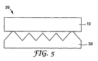
この目的のために、図5は本発明を耐ウェットアウト構造体に適用する光指向性物品39を示している。図5は光指向性フィルム38(図4)の上に設けられた光指向性フィルム10(図1)を示している。各フィルムのプリズム要素の線形のアレイは90°の角度で配向されている。光学結合を最小化するより高いプリズム要素は鈍い先端を有して形成される。或いは、両フィルムが耐スクラッチ性の場合、図6のフィルム38又はフィルム42のような別のフィルムが光指向性物品上に積層されてもよい。
For this purpose, FIG. 5 shows a light-directing
図6には別の実施形態を示している。図6は構造化表面44を有する光指向性フィルム42を示している。構造化表面44は鋭い先端34を有する第2のプリズム要素32と鈍い先端48を有する第3のプリズム要素46とを備えている。第2及び第3のプリズム要素32及び46は構造化表面44に沿って交互に配置されている。
FIG. 6 shows another embodiment. FIG. 6 shows a
ここで、図2及び図4に示したように実質的に平坦な先端部を有するより高いプリズム要素の代わりに、より高いプリズム要素は曲線状、すなわち放射状の先端部を有する。鈍い先端48の弦幅(第3のプリズム要素46の直線状の端部が曲線状の端部と出会う地点間の距離)とオンアクシス光の利得との関係が全く線形ではない場合を除き、鈍い先端48は鈍い先端30と実質的に同じように機能する。これは図3a及び図3bに示した関係(データは示さず)と類似する。従って、どのような形態の鈍い先端も本発明とともに使用され得る。
Here, instead of a higher prism element having a substantially flat tip as shown in FIGS. 2 and 4, the higher prism element has a curvilinear or radial tip. Unless the relationship between the chord width of the blunt tip 48 (the distance between the point where the linear end of the
図7は本発明の光指向性フィルムを組み込んだ光学ディスプレイ50の代表的な実施形態の断面図である。ディスプレイ50はケース52、光源54、光指向性フィルム56、光ゲートデバイス58、及びカバーシート60を備える。
FIG. 7 is a cross-sectional view of a representative embodiment of an
図7に示したように、光源54はエレクトロルミネセンスパネルであるが、ラップトップコンピュータに一般に用いられる蛍光バックライトアセンブリ、又は一部の計算機に一般に用いられる受動反射ディスプレイなどの他の光源は、本発明の範囲にあることを理解されたい。さらに、光ゲートデバイス58は液晶デバイスであることが好ましいが、他の光ゲートデバイスは本発明の範囲にある。図7には誇張しているが、光指向性フィルム56の先端が鈍いプリズム要素は、光指向性フィルム56の先端が鋭いプリズム要素よりも高いことが理解されよう。従って、先端が鋭いプリズム要素はさらに保護されて、光学ディスプレイに組み入れられる場合であっても損傷を受け難い。
As shown in FIG. 7, the
本発明を利用した光指向性フィルムは、フィルムが横に引っ張られるときに起こる引っかき傷を阻止する。従って、製造工程に応じて、本発明はプレマスクをフィルムに貼る必要性を回避し得る。 The light directing film utilizing the present invention prevents scratches that occur when the film is pulled sideways. Thus, depending on the manufacturing process, the present invention can avoid the need to apply a premask to the film.
フィルムに使用することのできる材料は種々ある。高い光透過性を保証するために材料は実質的に透明であることが不可欠である。有用な市販のポリマー材料の例には、公称屈折率がそれぞれ約1.493及び1.586であるポリアクリレート及びポリカーボネートが挙げられる。他の有用なポリマーにはポリプロピレン、ポリウレタン、ポリスチレン、塩化ポリビニル、及び他の同様の材料が挙げられる。特定の材料は決定的なものではないが、より高い屈折率を有する材料が好ましい。 There are various materials that can be used for the film. It is essential that the material be substantially transparent to ensure high light transmission. Examples of useful commercially available polymeric materials include polyacrylates and polycarbonates having nominal refractive indices of about 1.493 and 1.586, respectively. Other useful polymers include polypropylene, polyurethane, polystyrene, polyvinyl chloride, and other similar materials. The particular material is not critical, but materials with higher refractive indices are preferred.
本発明によるフィルムは種々の方法によって製造され得る。従来の方法には、ダイアモンド旋盤器などの精密工作機械を用いて機械加工可能な基材において金型を切ること、及びエンボス又はUV硬化法を用いてその金型を複製することが挙げられる。製造工程に応じて、これらのフィルムは典型的には約4ミル〜約20ミルの厚さである。 The film according to the invention can be produced by various methods. Conventional methods include cutting the mold on a substrate that can be machined using a precision machine tool such as a diamond lathe and replicating the mold using embossing or UV curing. Depending on the manufacturing process, these films are typically about 4 mils to about 20 mils thick.
Claims (22)
第1の表面と、
前記第1の表面と反対側の構造化表面であって、プリズム要素のアレイを有している構造化表面とを備えており、
該プリズム要素のアレイは、
前記第1の表面と前記構造化表面との間に配置された基準面から第1の距離に配置された鈍い先端を有する第1のプリズム要素と、
前記基準面から前記第1の距離よりも小さい第2の距離に配置された鋭い先端を有する第2のプリズム要素と、
をさらに有する、光指向性フィルム。 A light directing film,
A first surface;
A structured surface opposite the first surface, the structured surface having an array of prism elements;
The array of prism elements is
A first prism element having a blunt tip disposed at a first distance from a reference plane disposed between the first surface and the structured surface;
A second prism element having a sharp tip disposed at a second distance less than the first distance from the reference plane;
A light directing film further comprising:
第1の表面と、
前記第1の表面と反対側の構造化表面であって、前記構造化表面は、交互に配置された第1及び第2のプリズム要素のアレイを有し、前記第1のプリズム要素は外面を画定する鈍い先端を有し、前記第2のプリズム要素は前記外面に対して凹状になっている鋭い先端を有する、構造化表面と、
を備えた光指向性フィルム。 A light directing film,
A first surface;
A structured surface opposite the first surface, wherein the structured surface comprises an array of alternating first and second prism elements, the first prism element having an outer surface A structured surface having a blunt tip that defines, and wherein the second prism element has a sharp tip that is concave with respect to the outer surface;
Light directivity film with.
第1の表面と、
前記第1の表面と反対側の構造化表面であって、前記構造化表面は交互に配置された第1及び第2のプリズム要素のアレイを有し、前記第1のプリズム要素は少なくとも1つの外面を画定する鈍い先端を有し、前記第2のプリズム要素は少なくとも1つの内面を画定する鋭い先端を有する、構造化表面と、
を備えた光指向性フィルム。 A light directing film,
A first surface;
A structured surface opposite the first surface, wherein the structured surface comprises an array of alternating first and second prism elements, wherein the first prism element is at least one A structured surface having a blunt tip defining an outer surface, and wherein the second prism element has a sharp tip defining at least one inner surface;
Light directivity film with.
第1の表面と、
前記第1の表面と反対側の構造化表面であって、前記構造化表面は交互に配置された第1及び第2のプリズム要素のアレイを有し、前記第1のプリズム要素は複数の外面を画定する鈍い先端を有し、前記第2のプリズム要素は複数の内面を画定する鋭い先端を有し、前記内面は前記外面に対して凹状になっている、構造化表面と、
を備えた光指向性フィルム。 A light directing film,
A first surface;
A structured surface opposite the first surface, the structured surface having an array of alternating first and second prism elements, wherein the first prism element has a plurality of outer surfaces. A structured surface, wherein the second prism element has a sharp tip defining a plurality of inner surfaces, the inner surface being concave with respect to the outer surface;
Light directivity film with.
第1の表面、前記第1の表面と反対側の第1の構造化表面、及び前記第1の表面と前記第1の構造化表面との間にある基準面を有する第1の光指向性フィルムであって、前記第1の構造化表面は、第1の主軸に沿って配向された、第1のプリズム要素及び第2のプリズム要素の線形のアレイを有し、前記第1及び第2のプリズム要素は、少なくとも1つの第2のプリズム要素が少なくとも一対の第1のプリズム要素の間に挟み込まれる繰り返しパターンで配置されており、前記第1のプリズム要素は前記基準面から第1の距離に配置された鈍い先端を有し、且つ、前記第2のプリズム要素は前記第1の距離よりも小さい、前記基準面から第2の距離に配置された鋭い先端を有している、第1の光指向性フィルムと、
前記第1の光指向性フィルムの前記第1の構造化表面に隣接して配置された実質的に平坦な表面を有する第2の光指向性フィルムであって、前記第2の光指向性フィルムは、前記実質的に平坦な表面と反対側の第2の構造化表面を有し、前記第2の構造化表面は第2の主軸に沿って配向されたプリズム要素の線形のアレイを有している、第2の光指向性フィルムとを含み、
前記第1の主軸は前記第2の主軸と光学結合を最小にする角度で交差する、光指向性物品。 A light directing article,
A first light directivity having a first surface, a first structured surface opposite the first surface, and a reference surface between the first surface and the first structured surface A first structured surface having a linear array of first and second prism elements oriented along a first major axis, wherein the first and second Are arranged in a repeating pattern in which at least one second prism element is sandwiched between at least one pair of first prism elements, and the first prism element has a first distance from the reference plane. And the second prism element has a sharp tip disposed at a second distance from the reference plane that is less than the first distance. Light directivity film,
A second light directional film having a substantially flat surface disposed adjacent to the first structured surface of the first light directional film, wherein the second light directional film. Has a second structured surface opposite the substantially flat surface, the second structured surface having a linear array of prism elements oriented along a second major axis. A second light directing film,
The light directing article, wherein the first principal axis intersects the second principal axis at an angle that minimizes optical coupling.
光源と、
可視スクリーンと、
前記光源から前記視野スクリーンまで光を導く光搬送手段であって、該光搬送手段は少なくとも第1の光指向性フィルムを有し、前記光指向性フィルムは第1の表面、前記第1の表面と反対側の構造化表面、及び前記第1の表面と前記構造化表面との間にある基準面を有しており、前記構造化表面は、第1のプリズム要素及び第2のプリズム要素のアレイを有し、前記第1のプリズム要素は鈍い先端を有し、前記第2のプリズム要素は鋭い先端を有し、前記鈍い先端は前記基準面から第1の距離に配置され、前記鋭い先端は前記基準面から第2の距離に配置され、前記第2の距離は前記第1の距離よりも小さい、光搬送手段と、
を備えた光学ディスプレイ。 An optical display,
A light source;
A visible screen,
Light transporting means for guiding light from the light source to the field screen, the light transporting means having at least a first light directing film, the light directing film being a first surface, the first surface And a reference surface lying between the first surface and the structured surface, the structured surface comprising: a first prism element and a second prism element; An array, wherein the first prism element has a blunt tip, the second prism element has a sharp tip, the blunt tip is disposed at a first distance from the reference plane, and the sharp tip Is disposed at a second distance from the reference plane, and the second distance is smaller than the first distance;
With optical display.
Applications Claiming Priority (2)
| Application Number | Priority Date | Filing Date | Title |
|---|---|---|---|
| US10/750,328 US7142767B2 (en) | 2003-12-31 | 2003-12-31 | Scratch-resistant light directing films |
| PCT/US2004/037533 WO2005069045A1 (en) | 2003-12-31 | 2004-11-09 | Scratch-resistant light directing films |
Publications (2)
| Publication Number | Publication Date |
|---|---|
| JP2007517256A true JP2007517256A (en) | 2007-06-28 |
| JP2007517256A5 JP2007517256A5 (en) | 2007-11-08 |
Family
ID=34711257
Family Applications (1)
| Application Number | Title | Priority Date | Filing Date |
|---|---|---|---|
| JP2006546992A Withdrawn JP2007517256A (en) | 2003-12-31 | 2004-11-09 | Scratch resistant light directivity film |
Country Status (8)
| Country | Link |
|---|---|
| US (1) | US7142767B2 (en) |
| EP (1) | EP1700140A1 (en) |
| JP (1) | JP2007517256A (en) |
| KR (1) | KR20060115755A (en) |
| CN (1) | CN100420965C (en) |
| AU (1) | AU2004313596A1 (en) |
| TW (1) | TW200533963A (en) |
| WO (1) | WO2005069045A1 (en) |
Cited By (11)
| Publication number | Priority date | Publication date | Assignee | Title |
|---|---|---|---|---|
| JP2009265212A (en) * | 2008-04-23 | 2009-11-12 | Goyo Paper Working Co Ltd | Frictional flaw resistant prism sheet |
| JP2010113126A (en) * | 2008-11-06 | 2010-05-20 | Goyo Paper Working Co Ltd | Scratch-resistant prism sheet and method for producing the same |
| JP2010122628A (en) * | 2008-11-21 | 2010-06-03 | Toppan Printing Co Ltd | Optical sheet, back light unit and display device |
| JP2010160438A (en) * | 2009-01-09 | 2010-07-22 | Toppan Printing Co Ltd | Lens sheet, back light unit and display apparatus |
| JP2010160437A (en) * | 2009-01-09 | 2010-07-22 | Toppan Printing Co Ltd | Optical sheet, back light unit and display |
| JP2010164657A (en) * | 2009-01-13 | 2010-07-29 | Toppan Printing Co Ltd | Optical sheet, back light unit and display device |
| JP2010210882A (en) * | 2009-03-10 | 2010-09-24 | Toppan Printing Co Ltd | Optical sheet and display using the same |
| JP2010237397A (en) * | 2009-03-31 | 2010-10-21 | Kimoto & Co Ltd | Prism sheet and backlight using the same |
| JP2010243574A (en) * | 2009-04-01 | 2010-10-28 | Toppan Printing Co Ltd | Optical sheet, backlight unit, and display device |
| JP2010540271A (en) * | 2007-09-21 | 2010-12-24 | スリーエム イノベイティブ プロパティズ カンパニー | Optical film |
| JP2011064744A (en) * | 2009-09-15 | 2011-03-31 | Toppan Printing Co Ltd | Optical sheet, backlight unit, and display device |
Families Citing this family (41)
| Publication number | Priority date | Publication date | Assignee | Title |
|---|---|---|---|---|
| US7859759B2 (en) * | 2002-05-20 | 2010-12-28 | Sabic Innovative Plastics Ip B.V. | Film, backlight displays, and methods for making the same |
| US6952627B2 (en) * | 2002-12-18 | 2005-10-04 | General Electric Company | Method and apparatus for fabricating light management substrates |
| US7416309B2 (en) * | 2004-12-30 | 2008-08-26 | 3M Innovative Properties Company | Optical film having a surface with rounded structures |
| US7384173B2 (en) * | 2004-12-30 | 2008-06-10 | 3M Innovative Properties Company | Brightness enhancement article |
| US20060250707A1 (en) * | 2005-05-05 | 2006-11-09 | 3M Innovative Properties Company | Optical film having a surface with rounded pyramidal structures |
| KR101372024B1 (en) * | 2005-06-09 | 2014-03-07 | 유브라이트 옵트로닉스 코포레이션 | Moire reducing optical substrates with irregular prism structure |
| US20070024994A1 (en) * | 2005-07-29 | 2007-02-01 | 3M Innovative Properties Company | Structured optical film with interspersed pyramidal structures |
| US7866871B2 (en) | 2006-01-13 | 2011-01-11 | Avery Dennison Corporation | Light enhancing structures with a plurality of arrays of elongate features |
| US7674028B2 (en) * | 2006-01-13 | 2010-03-09 | Avery Dennison Corporation | Light enhancing structures with multiple arrays of elongate features of varying characteristics |
| KR100813255B1 (en) * | 2006-06-02 | 2008-03-13 | 삼성전자주식회사 | High output light guide panel, backlight unit employing the lightguide panel |
| US7643218B2 (en) * | 2006-08-31 | 2010-01-05 | Skc Haas Display Films Co., Ltd. | Light redirecting film having varying optical elements |
| CN100442084C (en) * | 2006-09-22 | 2008-12-10 | 长兴光学材料(苏州)有限公司 | Optical film and two-dimensional display device |
| JP4880697B2 (en) * | 2006-11-09 | 2012-02-22 | シャープ株式会社 | Prism sheet and liquid crystal display device |
| KR100796479B1 (en) | 2007-01-31 | 2008-01-21 | 미래나노텍(주) | Optical sheet and back light assembly equipped with the prism sheet |
| US20080247065A1 (en) * | 2007-04-06 | 2008-10-09 | 3M Innovative Properties Company | Method of making structured optical films |
| KR100905241B1 (en) * | 2007-04-13 | 2009-07-01 | 엘지전자 주식회사 | Optical film having a plurality of structures and backlight unit including the same |
| TW200848854A (en) * | 2007-06-06 | 2008-12-16 | Optivision Technology Inc | Optical film having surface structure |
| CN101630031B (en) * | 2007-11-16 | 2011-07-20 | 长兴化学工业股份有限公司 | Optical film |
| CN101470221B (en) * | 2007-12-26 | 2011-01-19 | 颖台科技股份有限公司 | Diffusion plate and backlight module using the same |
| US20090214828A1 (en) * | 2008-02-26 | 2009-08-27 | Vicki Herzl Watkins | Blunt tip prism film and methods for making the same |
| CN106154399A (en) * | 2008-04-02 | 2016-11-23 | 3M创新有限公司 | Light directing film and preparation method thereof |
| KR100898047B1 (en) * | 2008-10-17 | 2009-05-19 | 이대환 | Optical member and method of manufacturing the same |
| US7922344B2 (en) * | 2008-09-02 | 2011-04-12 | Avery Dennison Corporation | Metallized retroreflective sheeting with increased daytime brightness |
| KR101258902B1 (en) * | 2008-12-31 | 2013-05-07 | 엘지디스플레이 주식회사 | Prism sheet, back light unit and liquid crystal display device having thereof |
| US20100182700A1 (en) * | 2009-01-22 | 2010-07-22 | Itt Manufacturing Enterprises, Inc. | Low stray light veiling glare objective lens for night vision systems |
| JP2011180574A (en) * | 2009-10-30 | 2011-09-15 | Dainippon Printing Co Ltd | Optical sheet, surface light source apparatus, and transmissive display apparatus |
| CN102236122B (en) * | 2010-04-30 | 2012-12-19 | 中强光电股份有限公司 | Optical membrane |
| CN102313195B (en) | 2010-07-06 | 2014-06-18 | 乐金显示有限公司 | Apparatus for fabricating light guide panel and backlight unit having the light guide panel |
| WO2013063202A1 (en) * | 2011-10-25 | 2013-05-02 | Unipixel Displays, Inc. | Optimization of uv curing |
| CN102445722A (en) * | 2011-12-21 | 2012-05-09 | 北京康得新复合材料股份有限公司 | Prism-structured brightness enhancement film with scratch-resistant characteristic |
| CN102436020A (en) * | 2011-12-21 | 2012-05-02 | 北京康得新复合材料股份有限公司 | Scratching-resistant prism structure bright enhancement film |
| CN102445723A (en) * | 2011-12-21 | 2012-05-09 | 北京康得新复合材料股份有限公司 | Prism-structured brightness enhancement film with scratch-resistant characteristic |
| CN102455449A (en) * | 2011-12-21 | 2012-05-16 | 北京康得新复合材料股份有限公司 | Prism-structured brightness enhancement film with anti-scraping property |
| US8833959B2 (en) | 2012-02-02 | 2014-09-16 | Blackberry Limited | Display arrangement with optical structure for reducing halo effect |
| CN105425325A (en) * | 2012-08-22 | 2016-03-23 | 友辉光电股份有限公司 | Optical film |
| CN103018802B (en) * | 2012-11-30 | 2015-09-16 | 张家港康得新光电材料有限公司 | A kind of brightness enhancement film with anti-scratch function |
| WO2015072420A1 (en) * | 2013-11-13 | 2015-05-21 | シャープ株式会社 | Daylighting film |
| CN107003438B (en) | 2014-12-05 | 2019-07-02 | 盛科光学株式会社 | Diffusion sheet, lamination prismatic lens and laminated optical piece |
| CN105807360B (en) * | 2014-12-29 | 2019-02-26 | 中强光电股份有限公司 | Light guide plate and light source module |
| CN104614791B (en) * | 2015-01-23 | 2017-05-24 | 东莞市纳利光学材料有限公司 | Birghtness enhancement film with pyramid structure and manufacture method thereof |
| CN106772770A (en) * | 2017-01-03 | 2017-05-31 | 深圳市宝明科技股份有限公司 | A kind of light guide plate of composite construction |
Family Cites Families (16)
| Publication number | Priority date | Publication date | Assignee | Title |
|---|---|---|---|---|
| US3810804A (en) * | 1970-09-29 | 1974-05-14 | Rowland Dev Corp | Method of making retroreflective material |
| US4101324A (en) * | 1974-09-26 | 1978-07-18 | Asahi Kasei Kogyo Kabushiki Kaisha | Printing plate and method for forming the same having small projections in non-image areas |
| US5122902A (en) * | 1989-03-31 | 1992-06-16 | Minnesota Mining And Manufacturing Company | Retroreflective articles having light-transmissive surfaces |
| CA2097109C (en) * | 1992-06-01 | 2000-01-11 | Shozo Kokawa | Liquid crystal display |
| US5614286A (en) | 1993-10-20 | 1997-03-25 | Minnesota Mining And Manufacturing Company | Conformable cube corner retroreflective sheeting |
| DE69429924T2 (en) * | 1993-10-20 | 2002-08-22 | Minnesota Mining And Mfg. Co., Saint Paul | DIRECTLY MANUFACTURED STAGE-STRUCTURED RETRORE-REFLECTIVE CUBE-CORNER BODY AND PRODUCTION METHOD |
| US5600484A (en) * | 1993-10-20 | 1997-02-04 | Minnesota Mining And Manufacturing Company | Machining techniques for retroreflective cube corner article and method of manufacture |
| US5657408A (en) * | 1994-12-23 | 1997-08-12 | Alliedsignal Inc. | Optical device comprising a plurality of units having at least two geometrically-differentiated tapered optical waveguides therein |
| KR100398940B1 (en) * | 1995-03-03 | 2003-12-31 | 미네소타 마이닝 앤드 매뉴팩춰링 캄파니 | A light directing film having a structure screen of various heights and an article comprising such a film |
| JP3473882B2 (en) | 1996-02-20 | 2003-12-08 | 株式会社エンプラス | Light guide plate and side light type surface light source device |
| US5919551A (en) | 1996-04-12 | 1999-07-06 | 3M Innovative Properties Company | Variable pitch structured optical film |
| US6021559A (en) * | 1996-11-01 | 2000-02-08 | 3M Innovative Properties Company | Methods of making a cube corner article master mold |
| RU2183336C2 (en) | 2000-07-21 | 2002-06-10 | Молохина Лариса Аркадьевна | Flexible light-returning material |
| JP3544349B2 (en) * | 2000-09-27 | 2004-07-21 | シャープ株式会社 | Liquid crystal display |
| DE10058074A1 (en) | 2000-11-23 | 2002-06-06 | Vitalij Lissotschenko | Method for producing a micro-optical functional unit |
| US7074463B2 (en) * | 2003-09-12 | 2006-07-11 | 3M Innovative Properties Company | Durable optical element |
-
2003
- 2003-12-31 US US10/750,328 patent/US7142767B2/en not_active Expired - Lifetime
-
2004
- 2004-11-09 WO PCT/US2004/037533 patent/WO2005069045A1/en active Application Filing
- 2004-11-09 AU AU2004313596A patent/AU2004313596A1/en not_active Abandoned
- 2004-11-09 EP EP04800971A patent/EP1700140A1/en not_active Withdrawn
- 2004-11-09 CN CNB2004800393965A patent/CN100420965C/en not_active Expired - Fee Related
- 2004-11-09 KR KR1020067012996A patent/KR20060115755A/en not_active Application Discontinuation
- 2004-11-09 JP JP2006546992A patent/JP2007517256A/en not_active Withdrawn
- 2004-11-23 TW TW093136005A patent/TW200533963A/en unknown
Cited By (13)
| Publication number | Priority date | Publication date | Assignee | Title |
|---|---|---|---|---|
| JP2010540271A (en) * | 2007-09-21 | 2010-12-24 | スリーエム イノベイティブ プロパティズ カンパニー | Optical film |
| US8885256B2 (en) | 2007-09-21 | 2014-11-11 | 3M Innovative Properties Company | Optical film |
| US8503082B2 (en) | 2007-09-21 | 2013-08-06 | 3M Innovative Properties Company | Optical film |
| JP2009265212A (en) * | 2008-04-23 | 2009-11-12 | Goyo Paper Working Co Ltd | Frictional flaw resistant prism sheet |
| JP2010113126A (en) * | 2008-11-06 | 2010-05-20 | Goyo Paper Working Co Ltd | Scratch-resistant prism sheet and method for producing the same |
| JP2010122628A (en) * | 2008-11-21 | 2010-06-03 | Toppan Printing Co Ltd | Optical sheet, back light unit and display device |
| JP2010160438A (en) * | 2009-01-09 | 2010-07-22 | Toppan Printing Co Ltd | Lens sheet, back light unit and display apparatus |
| JP2010160437A (en) * | 2009-01-09 | 2010-07-22 | Toppan Printing Co Ltd | Optical sheet, back light unit and display |
| JP2010164657A (en) * | 2009-01-13 | 2010-07-29 | Toppan Printing Co Ltd | Optical sheet, back light unit and display device |
| JP2010210882A (en) * | 2009-03-10 | 2010-09-24 | Toppan Printing Co Ltd | Optical sheet and display using the same |
| JP2010237397A (en) * | 2009-03-31 | 2010-10-21 | Kimoto & Co Ltd | Prism sheet and backlight using the same |
| JP2010243574A (en) * | 2009-04-01 | 2010-10-28 | Toppan Printing Co Ltd | Optical sheet, backlight unit, and display device |
| JP2011064744A (en) * | 2009-09-15 | 2011-03-31 | Toppan Printing Co Ltd | Optical sheet, backlight unit, and display device |
Also Published As
| Publication number | Publication date |
|---|---|
| EP1700140A1 (en) | 2006-09-13 |
| CN1902511A (en) | 2007-01-24 |
| TW200533963A (en) | 2005-10-16 |
| US7142767B2 (en) | 2006-11-28 |
| AU2004313596A1 (en) | 2005-07-28 |
| KR20060115755A (en) | 2006-11-09 |
| WO2005069045A1 (en) | 2005-07-28 |
| CN100420965C (en) | 2008-09-24 |
| US20050147374A1 (en) | 2005-07-07 |
Similar Documents
| Publication | Publication Date | Title |
|---|---|---|
| JP2007517256A (en) | Scratch resistant light directivity film | |
| KR100398940B1 (en) | A light directing film having a structure screen of various heights and an article comprising such a film | |
| JP5823958B2 (en) | Light re-deflecting film and display using the film | |
| US7367705B2 (en) | Long curved wedges in an optical film | |
| EP2870494B1 (en) | Decorative film articles utilizing fresnel lens films | |
| US8888333B2 (en) | Light redirecting film and display system incorporating same | |
| CN107533188B (en) | Optical film | |
| JP2009503562A (en) | Turning film with variable pitch | |
| TWI374315B (en) | ||
| CN101231349A (en) | Microstructured film containing polysulfone polymer | |
| KR20140041539A (en) | Light management film | |
| KR20130077708A (en) | Prism sheet, back light unit comprising the same and optical display apparatus comprising the same | |
| US7845811B2 (en) | Prism sheet and liquid crystal display device using the same | |
| US20140375929A1 (en) | Light management film | |
| US7845810B2 (en) | Prism sheet and liquid crystal display device using the same | |
| TWI553349B (en) | Optical sheet | |
| JP2005308789A (en) | Reflector and liquid crystal display device using the same | |
| KR20160017206A (en) | Light guide plate, method for preparing the same, back light unit comprising the same and liquid crystal display comprising the same | |
| KR20160017205A (en) | Light guide plate, method for preparing the same, back light unit comprising the same and liquid crystal display comprising the same |
Legal Events
| Date | Code | Title | Description |
|---|---|---|---|
| A521 | Request for written amendment filed |
Free format text: JAPANESE INTERMEDIATE CODE: A523 Effective date: 20070920 |
|
| A621 | Written request for application examination |
Free format text: JAPANESE INTERMEDIATE CODE: A621 Effective date: 20070920 |
|
| A761 | Written withdrawal of application |
Free format text: JAPANESE INTERMEDIATE CODE: A761 Effective date: 20090610 |