JP2007514389A - Wire harness and touch sensor incorporating it - Google Patents
Wire harness and touch sensor incorporating it Download PDFInfo
- Publication number
- JP2007514389A JP2007514389A JP2006545680A JP2006545680A JP2007514389A JP 2007514389 A JP2007514389 A JP 2007514389A JP 2006545680 A JP2006545680 A JP 2006545680A JP 2006545680 A JP2006545680 A JP 2006545680A JP 2007514389 A JP2007514389 A JP 2007514389A
- Authority
- JP
- Japan
- Prior art keywords
- touch
- touch sensor
- sensor according
- dielectric substrate
- electrode
- Prior art date
- Legal status (The legal status is an assumption and is not a legal conclusion. Google has not performed a legal analysis and makes no representation as to the accuracy of the status listed.)
- Withdrawn
Links
Images


Classifications
-
- G—PHYSICS
- G06—COMPUTING; CALCULATING OR COUNTING
- G06F—ELECTRIC DIGITAL DATA PROCESSING
- G06F3/00—Input arrangements for transferring data to be processed into a form capable of being handled by the computer; Output arrangements for transferring data from processing unit to output unit, e.g. interface arrangements
- G06F3/01—Input arrangements or combined input and output arrangements for interaction between user and computer
- G06F3/03—Arrangements for converting the position or the displacement of a member into a coded form
- G06F3/041—Digitisers, e.g. for touch screens or touch pads, characterised by the transducing means
- G06F3/045—Digitisers, e.g. for touch screens or touch pads, characterised by the transducing means using resistive elements, e.g. a single continuous surface or two parallel surfaces put in contact
-
- G—PHYSICS
- G06—COMPUTING; CALCULATING OR COUNTING
- G06F—ELECTRIC DIGITAL DATA PROCESSING
- G06F3/00—Input arrangements for transferring data to be processed into a form capable of being handled by the computer; Output arrangements for transferring data from processing unit to output unit, e.g. interface arrangements
- G06F3/01—Input arrangements or combined input and output arrangements for interaction between user and computer
- G06F3/03—Arrangements for converting the position or the displacement of a member into a coded form
- G06F3/041—Digitisers, e.g. for touch screens or touch pads, characterised by the transducing means
- G06F3/044—Digitisers, e.g. for touch screens or touch pads, characterised by the transducing means by capacitive means
- G06F3/0444—Digitisers, e.g. for touch screens or touch pads, characterised by the transducing means by capacitive means using a single conductive element covering the whole sensing surface, e.g. by sensing the electrical current flowing at the corners
-
- G—PHYSICS
- G06—COMPUTING; CALCULATING OR COUNTING
- G06F—ELECTRIC DIGITAL DATA PROCESSING
- G06F3/00—Input arrangements for transferring data to be processed into a form capable of being handled by the computer; Output arrangements for transferring data from processing unit to output unit, e.g. interface arrangements
- G06F3/01—Input arrangements or combined input and output arrangements for interaction between user and computer
- G06F3/03—Arrangements for converting the position or the displacement of a member into a coded form
- G06F3/041—Digitisers, e.g. for touch screens or touch pads, characterised by the transducing means
- G06F3/0416—Control or interface arrangements specially adapted for digitisers
Abstract
ワイヤハーネスおよびそれを組み込んでいるタッチセンサーが開示される。このタッチセンサーは、タッチ感知領域に配設される検知電極を含む。タッチセンサーは、境界領域において自立誘電体基板上に配設される複数の補助電極をさらに含む。この補助電極は、タッチ信号を、このタッチ信号を用いてタッチ位置を決定するように構成される電子機器に送信する。 A wire harness and a touch sensor incorporating the same are disclosed. The touch sensor includes a detection electrode disposed in the touch sensing area. The touch sensor further includes a plurality of auxiliary electrodes disposed on the free-standing dielectric substrate in the boundary region. The auxiliary electrode transmits a touch signal to an electronic device configured to determine a touch position using the touch signal.
Description
本発明は、一般に、検知装置に関する。本発明は、特にタッチパネルと一体のワイヤハーネスを有するタッチセンサーに適用可能である。 The present invention generally relates to sensing devices. The present invention is particularly applicable to a touch sensor having a wire harness integrated with a touch panel.
タッチスクリーンにより、ユーザは、キーボードの必要性を減らすかまたは失くすることによって、電子表示システムと都合良くインターフェースをとることができる。例えば、ユーザは、予めプログラムされたアイコンによって識別される位置でただスクリーンに触れるだけで、複雑な一連の命令を実行することができる。オンスクリーンメニュー(on-screen menu)は、用途によって、支持ソフトウエアを予めプログラムすることによって変更することができる。他の例として、タッチスクリーンにより、ユーザが、テキストまたは図面を、タッチスクリーン上へ直接書込むかまたは描画によって、電子表示装置に転送することができる。 A touch screen allows a user to conveniently interface with an electronic display system by reducing or eliminating the need for a keyboard. For example, a user can execute a complex series of commands by simply touching the screen at a location identified by a pre-programmed icon. Depending on the application, the on-screen menu can be changed by pre-programming the support software. As another example, a touch screen allows a user to transfer text or drawings to an electronic display device by writing or drawing directly on the touch screen.
タッチ入力の位置を検出するために使用される二つの共通のタッチ検知方法としては、抵抗性および容量性のものがある。抵抗性技術は、典型的には、2つの透明導電膜を、タッチの位置を検出する電子回路の一部として組み込む。他方、容量性技術は、典型的には、1つの透明導電膜を用いて、加えられたタッチの位置を検出する。 Two common touch sensing methods used to detect the position of touch input are resistive and capacitive. Resistive technology typically incorporates two transparent conductive films as part of an electronic circuit that detects the position of the touch. On the other hand, capacitive technology typically uses a single transparent conductive film to detect the position of an applied touch.
タッチセンサーは、一般に、タッチパネル、およびそのタッチパネルに加えられるタッチ入力に応答して発生されるタッチ信号を検出する電子回路を含む。この電子回路は、検出されたタッチ信号を用いて、加えられたタッチの位置を決定する。一般に、各々がタッチパネルの外にある多数の個々のワイヤは、タッチパネルを電子回路に電気的に接続するために用いられる。個々のワイヤをタッチパネルに接続することは、通常手作業でなされるので手間がかかり、また接続は、しばしば信頼性がなく、パネルを損傷することがあり、パネルを動作不能にすることさえある。 The touch sensor generally includes a touch panel and an electronic circuit that detects a touch signal generated in response to a touch input applied to the touch panel. The electronic circuit uses the detected touch signal to determine the position of the applied touch. In general, a number of individual wires, each outside the touch panel, are used to electrically connect the touch panel to an electronic circuit. Connecting individual wires to the touch panel is usually manual and laborious, and the connection is often unreliable, can damage the panel, and can even render the panel inoperable.
一般に、本発明は、ワイヤハーネスに関する。本発明はまた、ワイヤハーネスを組み込んだ検知装置に関する。 In general, the present invention relates to a wire harness. The present invention also relates to a detection device incorporating a wire harness.
本発明の一態様では、タッチセンサーは、タッチ感知領域を覆うセンサー基板を含む。このタッチ感知領域は、タッチセンサーの前側面からこのタッチ感知領域に加えられるタッチ入力を受けるように構成される。タッチセンサーは、タッチ感知領域においてセンサー基板上に配設される検知電極をさらに含む。タッチセンサーは、境界領域を覆う自立誘電体基板をさらに含む。この境界領域は、タッチ感知領域の外部にある。上記の誘電体基板は、検知電極とタッチセンサーの前側面との間に配設される。タッチセンサーは、境界領域において自立誘電体基板上に配設される複数の補助電極をさらに含む。タッチセンサーは、タッチセンサーの前側面からタッチ感知領域に加えられるタッチ入力に応答して、タッチ信号を検知電極に発生する。この補助電極は、上記のタッチ信号を電子機器に送信する。電子機器は、このタッチ信号を用いて、タッチ位置を決定するように構成される。 In one aspect of the present invention, the touch sensor includes a sensor substrate that covers the touch sensing area. The touch sensitive area is configured to receive a touch input applied to the touch sensitive area from the front side of the touch sensor. The touch sensor further includes a sensing electrode disposed on the sensor substrate in the touch sensing area. The touch sensor further includes a free-standing dielectric substrate that covers the boundary region. This border area is outside the touch sensitive area. The dielectric substrate is disposed between the detection electrode and the front side surface of the touch sensor. The touch sensor further includes a plurality of auxiliary electrodes disposed on the free-standing dielectric substrate in the boundary region. The touch sensor generates a touch signal on the detection electrode in response to a touch input applied to the touch sensing area from the front side of the touch sensor. The auxiliary electrode transmits the touch signal to the electronic device. The electronic device is configured to determine a touch position using the touch signal.
本発明の他の態様では、容量性タッチセンサーは、タッチ感知領域を覆うセンサー基板を含む。タッチ感知領域は、このタッチ感知領域に加えられるタッチ入力を受けるように構成される。タッチセンサーは、タッチ感知領域においてセンサー基板上に配設される検知電極をさらに含む。タッチセンサーは、境界領域を覆う自立誘電体基板をさらに含む。この境界領域は、タッチ感知領域の外部にある。タッチセンサーは、境界領域において誘電体基板上に配設される複数の補助電極をさらに含む。タッチセンサーは、タッチセンサーとタッチ感知領域に加えられるタッチ入力との間の容量性カップリングに応答して、タッチ信号を発生する。上記の補助電極は、このタッチ信号を電子機器に送信する。電子機器は、このタッチ信号を用いて、タッチ位置を決定するように構成される。 In another aspect of the invention, the capacitive touch sensor includes a sensor substrate that covers the touch sensitive area. The touch sensitive area is configured to receive a touch input applied to the touch sensitive area. The touch sensor further includes a sensing electrode disposed on the sensor substrate in the touch sensing area. The touch sensor further includes a free-standing dielectric substrate that covers the boundary region. This border area is outside the touch sensitive area. The touch sensor further includes a plurality of auxiliary electrodes disposed on the dielectric substrate in the boundary region. The touch sensor generates a touch signal in response to capacitive coupling between the touch sensor and a touch input applied to the touch sensitive area. The auxiliary electrode transmits the touch signal to the electronic device. The electronic device is configured to determine a touch position using the touch signal.
本発明は、添付の図面に関連して、本発明のさまざまな実施形態の下記の詳細な説明を考慮してより完全に理解されかつ認識されよう。 The present invention will be understood and appreciated more fully upon consideration of the following detailed description of various embodiments of the invention in connection with the accompanying drawings.
本発明は、さまざまな修正および代替形態に変更可能であるが、その具体例を、図面に例によって示し、詳細に説明する。しかしながら、本発明は、記載される特定の実施形態に限定されるべきでないことは理解されたい。それどころか、本発明は、本発明の精神および範囲に入る全ての修正、等価なもの、および代替を包含するものである。 While the invention is susceptible to various modifications and alternative forms, specific examples thereof are shown by way of example in the drawings and will be described in detail. However, it should be understood that the invention should not be limited to the specific embodiments described. On the contrary, the invention is intended to cover all modifications, equivalents, and alternatives falling within the spirit and scope of the invention.
本出願は、タッチ入力検知装置(TOUCH INPUT SENSING DEVICE)という名称の、2003年10月6日に出願された特許出願第10/679903号に関連する。 This application is related to patent application No. 10/679903, filed Oct. 6, 2003, named TOUCH INPUT SENSING DEVICE.
本発明は、一般に、タッチセンサー(touch sensor)に関する。本発明は、詳細には、一体形ワイヤハーネス(integral wiring harness)を有するタッチセンサーに適用可能であり、より詳細には、一体形ワイヤハーネスを有する容量性および抵抗性タッチセンサーに適用可能である。 The present invention generally relates to touch sensors. The present invention is particularly applicable to touch sensors having an integral wiring harness, and more particularly to capacitive and resistive touch sensors having an integral wiring harness. .
タッチスクリーンは、タッチが加えられると、そうでなければ開いている電気回路が閉じられるという一般的な原理で機能する。閉じられた回路で発生される信号の特性によって、タッチ位置の検出が可能となる。さまざまな技術を、タッチ位置を検出するために使用することができる。このような技術の1つは抵抗性のものである。抵抗性タッチでは、加えられたタッチが、そうでなければ物理的に分離されている2つの導電膜を互いに直接物理的に接触させる。この物理的接触が、そうでなければ開いている電子回路を閉じ、その結果抵抗的に結合された電気信号が発生される。発生された信号の特性によって、タッチ位置の検出が可能になる。 Touch screens work on the general principle that when a touch is applied, an open electrical circuit is closed otherwise. The touch position can be detected by the characteristics of the signal generated by the closed circuit. Various techniques can be used to detect the touch location. One such technique is resistive. In a resistive touch, the applied touch brings two conductive films that are otherwise physically separated into direct physical contact with each other. This physical contact closes the otherwise open electronic circuit, resulting in a resistively coupled electrical signal. The touch position can be detected according to the characteristics of the generated signal.
タッチ入力の位置を検出するために一般に用いられる技術は容量性のものである。この場合には、ユーザの指などの導電性タッチ手段が導電膜に十分接近して来ることにより2つの導体間の容量性カップリングが可能となると、信号が発生される。この2つの導体を、例えば接地を通して、互いに電気的に接続することができる。 A commonly used technique for detecting the position of touch input is capacitive. In this case, a signal is generated when the capacitive touch between the two conductors is possible because the conductive touch means, such as the user's finger, is sufficiently close to the conductive film. The two conductors can be electrically connected to each other, for example through ground.
タッチセンサーはディジタルでもアナログでもよい。ディジタルセンサーのタッチ感知領域(touch sensitive area)は複数の別個の電気的に絶縁された導電膜を含む。例えば、タッチ感知領域は一組の別個のタッチパッド(touch pad)を含んでもよい。他の例として、タッチ感知領域は、複数の電気的に絶縁された平行な横列または縦列の導電膜を含むことができる。ディジタルタッチセンサーでは、タッチ入力の座標は、タッチによって誘導される離散的あるいは等価的に区別可能な信号を用いることによって決定することができる。アナログタッチセンサーでは、タッチ感知領域は、典型的には、電気的に連続する導電膜によって覆われる。このような場合には、タッチ入力によって誘導される信号は、非離散的と見なせる、あるいは等価的に一組の連続する可能な値の任意の一つと見なすことができる信号を含むことができる。アナログタッチセンサーでは、タッチ入力の座標は、タッチによって誘導される連続する信号を検出して使用することによって決定することができる。タッチ位置を決定する精度は、誘導された信号を処理するために用いられる電子機器(electronics)によって制限され得る。 The touch sensor may be digital or analog. The touch sensitive area of the digital sensor includes a plurality of separate electrically isolated conductive films. For example, the touch sensitive area may include a set of separate touch pads. As another example, the touch sensitive region can include a plurality of electrically isolated parallel row or column conductive films. In a digital touch sensor, the coordinates of touch input can be determined by using discrete or equivalently distinguishable signals induced by touch. In an analog touch sensor, the touch sensitive area is typically covered by an electrically continuous conductive film. In such a case, the signal induced by the touch input can include a signal that can be considered non-discrete or equivalently any one of a set of consecutive possible values. In an analog touch sensor, the coordinates of the touch input can be determined by detecting and using successive signals induced by the touch. The accuracy of determining the touch location can be limited by the electronics used to process the derived signal.
タッチセンサーは、典型的に、多数の外部電気絶縁ワイヤ、しばしば4本のワイヤを用いて、タッチ誘導信号を、タッチパネル上の多数のピックアップ位置から、タッチ信号を処理するための電子回路に送信する。典型的に、各外部ワイヤは、タッチパネルの縁部に沿ってその周りに伸びる。外部ワイヤとピックアップ位置との間の電気的接続は、ワイヤを、ピックアップ位置でタッチパネルに手ではんだ付けすることによってしばしば行なわれる。従って、この工程は、かなり手間がかかり、それゆえ高価であり得る。はんだ付けの結果、高プロファイルのはんだバンプ(solder bump)を生じることがあり、従ってタッチパネルのプロファイル全体に悪影響を及ぼす場合がある。はんだバンプは、例えば、他の部品との接触からあるいは処理および組立中、損傷を受けやすく、それによってタッチ位置の精度を損なう場合がある。さらに、はんだ付けされた接続部は、接合部で破損することがあり、またはその他、はんだ付けされた外部ワイヤが、例えば処理中偶然に引っ張られる場合、電気的に故障することがある。さらに、はんだ付け温度は、容易に150℃を超えることがある。高温は、導電性コーティング、および基板あるいはアンチグレア(anti-glare)またはアンチニュートンリング(anti-Newton-ring)コーティングなどのさまざまな光学層などの付近の部品を損傷することがある。 Touch sensors typically use multiple external electrically insulated wires, often 4 wires, to transmit touch induction signals from multiple pickup locations on the touch panel to electronic circuitry for processing the touch signals. . Typically, each external wire extends around the edge of the touch panel. The electrical connection between the external wire and the pickup location is often made by manually soldering the wire to the touch panel at the pickup location. This process is therefore quite labor intensive and can therefore be expensive. Soldering can result in high profile solder bumps, and thus can adversely affect the entire touch panel profile. Solder bumps can be susceptible to damage, for example, from contact with other components or during processing and assembly, thereby compromising touch location accuracy. In addition, the soldered connection can break at the joint, or otherwise, the soldered external wire can fail electrically, for example if it is accidentally pulled during processing. Furthermore, the soldering temperature can easily exceed 150 ° C. High temperatures can damage nearby components such as conductive coatings and various optical layers such as substrates or anti-glare or anti-Newton-ring coatings.
ワイヤハーネス(wire harness)は、タッチ位置を決定するのを妨げることがある電気雑音またはその他の信号から保護されるのが一般に望ましい。このような保護は、一般に、タッチパネルの縁部に沿って、ワイヤ上に誘電テープを配置することによって提供される。このテープは、適所にしばしば手作業で配置され、タッチパネルに不完全な仕上げの外観を与える。さらに、テーピング処理は手間がかかり、それゆえ高価であり得る。 It is generally desirable that the wire harness be protected from electrical noise or other signals that can interfere with determining the touch location. Such protection is generally provided by placing a dielectric tape on the wire along the edge of the touch panel. This tape is often manually placed in place, giving the touch panel an incompletely finished appearance. Furthermore, the taping process is laborious and can therefore be expensive.
一体形配線トレース(integral wiring trace)を有するタッチパネルは、例えば、米国特許出願第2001/0028343号および同第2001/0036504号に開示されている。 Touch panels having an integral wiring trace are disclosed, for example, in US Patent Application Nos. 2001/0028343 and 2001/0036504.
本発明は、一体形ワイヤハーネスを含むタッチセンサーについて記載し、ここで、「一体形」とは、ワイヤハーネスが、タッチパネル内の一つ以上の部品または層の上に形成されることを意味する。ワイヤハーネスは、例えば、タッチパネルの縁部(edge)に沿ってその周りに、所望のパターンで導電性インクをスクリーン印刷(screen printing)することによって、例えば、誘電体基板上に形成される。従って、本発明は、ワイヤハーネスをタッチセンサーにはんだ付けする必要性を失くするかあるいは減らす。その結果、本発明は、タッチパネル内のはんだバンプの数を減らすか、あるいははんだバンプを全く除去することが可能である。 The present invention describes a touch sensor that includes an integral wire harness, where “integral” means that the wire harness is formed on one or more components or layers in the touch panel. . The wire harness is formed on a dielectric substrate, for example, by screen printing conductive ink in a desired pattern around the edge of the touch panel. Thus, the present invention eliminates or reduces the need to solder the wire harness to the touch sensor. As a result, the present invention can reduce the number of solder bumps in the touch panel or eliminate the solder bumps at all.
さらに、本発明の一実施形態によれば、一体形ワイヤハーネスが、タッチパネルの層間に配設され、このハーネスを目に見えなくするかあるいは目に見えにくくする。ワイヤハーネスは、ワイヤハーネスを形成することが抵抗性層(resistive layer)を損傷しないように、抵抗性層を含まない基板上に形成することもできる。 Furthermore, according to one embodiment of the present invention, an integral wire harness is disposed between the layers of the touch panel, making the harness invisible or invisible. The wire harness can also be formed on a substrate that does not include a resistive layer so that forming the wire harness does not damage the resistive layer.
本発明の一実施形態では、一体形ワイヤハーネスは、タッチセンサーの導電層と前側面との間に配設される。本発明の他の実施形態によれば、ワイヤハーネスは、タッチパネル内に配設される自立誘電体層(self-supporting dielectric layer)上に形成される。 In one embodiment of the invention, the integrated wire harness is disposed between the conductive layer and the front side of the touch sensor. According to another embodiment of the present invention, the wire harness is formed on a self-supporting dielectric layer disposed in the touch panel.
図1は、本発明の特定の一実施形態によるタッチセンサー100の概略側面図を示す。タッチセンサー100は、センサー基板110、センサー基板上に配設される検知電極120、自立誘電体基板130、および自立誘電体基板上に配設される複数の補助電極150を含む。
FIG. 1 shows a schematic side view of a
センサー基板110は、第1側面111および第2側面112を含む。自立誘電体基板130は、第1側面131および第2側面132を含む。
The
タッチセンサー100は、図1に点線160として示される前側面をさらに含む。タッチセンサーの前側面とは、それからタッチ入力がタッチセンサーに加えられる側面を意味する。例えば、図1では、タッチアプリケーター(touch applicator)190は、例えばセンサー基板110の第1側面111からではなく、側面160からタッチセンサー100に加えられる。第1側面131は、本発明のある実施形態では、タッチパネルの前側面160と一致することが可能であるが、点線160は、自立誘電体基板130の第1側面131から分離して示されている。その他の部品、基板および層は、タッチセンサーの前側面160と自立誘電体基板130との間に配設することができる。例としては、ハードコート(hard coat)、反射防止コーティング、汚れ防止コーティング、導電性コーティング、追加の基板、偏光膜(polarizer film)、リターダ膜(retarder film)、およびタッチセンサーで用いられるのに適するどのような膜または部品も含まれる。
タッチセンサー100は、タッチ感知領域140をさらに含む。この領域140は、タッチセンサーの前側面160からタッチ感知領域に加えられる、タッチ手段(touch implement)190からのタッチ入力(「X」によって示される)を受けるように構成される。さらに、タッチセンサー100は、タッチ感知領域140の外部に境界領域(border area)170を含む。本発明の一実施形態によれば、境界領域170は、加えられた入力タッチに対して反応しなく、これは、タッチセンサー100が、タッチパネルの前側面から境界領域170に加えられるタッチ入力に応答してタッチ信号を発生することはないことを意味している。ある実施形態では、境界領域170の一部または全てが、例えば、タッチセンサーのセンサー基板110の側面などの、タッチセンサーの他の側面から加えられるタッチ入力に対して反応してもよい。
The
タッチセンサー100は、境界領域170において自立誘電体基板130上に配設される複数の補助電極150をさらに含む。補助電極150は、外部電極198を経て電子機器199に送信するためにタッチ入力から発生される信号を受信するように構成される。例えば、タッチセンサー100は、タッチセンサーの前側面160から、タッチ感知領域160の位置Xに加えられるタッチ入力に応答して検知電極120にタッチ信号を発生させると、この発生されたタッチ信号を、このタッチ信号を用いてタッチ位置Xを決定することができる電子機器199に送信することができる。発生されたタッチ信号は、タッチパネル101上の多数の位置から、補助電極150によって送信されてもよい。例えば、発生されたタッチ信号は、検知電極120上の多数の位置、例えば、4つの位置から送信されてもよい。長方形のタッチ感知領域140では、4つの位置は、例えば、タッチ感知領域の4つの角の近くとすることができる。
本発明の一実施形態によれば、自立誘電体基板130は、可撓性である。自立誘電体基板130は、ガラスまたはポリマー製にすることができる。典型的な高分子材料には、ポリカーボネート、アクリル、ポリエチレンテレフタレート(PET)、ポリ塩化ビニル(PVC)、ポリスルホン(polysulfone)などがある。典型的なガラス材料には、ソーダ石灰ガラス、ホウケイ酸ガラス、ホウ酸塩ガラス(borate glass)、ケイ酸塩ガラス(silicate glass)、任意の酸化物ガラス(oxide glass)および石英ガラスがある。高分子基板130は、ガラスでできている類似の基板よりはるかに柔らかく、従って引っかき傷の影響をより受けやすいことがある。例えば、鉛筆硬度試験(ASTM D 3363、鉛筆試験による膜硬度についての試験方法(Test Method for Film Hardness by Pencil Test)を参照されたい)によれば、PETはほぼ1Hの鉛筆硬度を有し、一方ガラスはほぼ6Hのはるかに高い硬度を有する。
According to one embodiment of the present invention, the free standing
自立誘電体基板130は可撓性であるのが好ましく、これは、基板130が、層を構造的に損傷することなく曲げることができるほど十分薄いことを意味する。しかしながら、ある用途では、誘電体基板130は剛性であってもよい。ガラス自立誘電体基板130は、好ましくは、1500〜600mmにおよぶ曲率半径まで、より好ましくは、1400〜500mmの範囲まで、またさらには、1200〜400mmの範囲まで曲がることができるほど十分薄いことがより好ましい。本発明の一態様では、ガラス自立誘電体基板130は、好ましくは、0.1〜2.0mmの範囲、またより好ましくは、0.3〜1.5mmの範囲、そしてさらには、0.5〜1.0mmの範囲の厚さを有することがより好ましい。
The free standing
本発明の異なる実施形態は、タッチセンサーまたはタッチ表示システムにおける一層以上を、磨耗、引っかき傷、湿気および酸素などの環境要因、またはその他のいかなる外部からの要因からも保護するのが望ましい用途において利用することができる。 Different embodiments of the present invention are utilized in applications where it is desirable to protect one or more of the touch sensor or touch display system from environmental factors such as wear, scratches, moisture and oxygen, or any other external factors. can do.
検知電極120は、金属、半導体、ドープ半導体(doped semiconductor)、半金属(semi-metal)、金属酸化物、有機導体(organic conductor)、導電性ポリマーなどであり得る。典型的な金属導体には、金、銅、銀などがある。典型的な無機材料には、透明導電性酸化物(transparent conductive oxide)、例えば、インジウムスズ酸化物(indium tin oxide:ITO)、フッ素ドープスズ酸化物(fluorine doped tin oxide)、スズアンチモン酸化物(tin antimony oxide:TAO)などがある。典型的な有機材料には、欧州特許公報第EP-1-172-831-A2に開示されるもののようなポリピロール、ポリアニリン、ポリアセチレン、およびポリチオフェンなどの導電性ポリマーがある。検知電極120のシート抵抗(sheet resistance)は、50〜100,000オーム/スクエア(Ohms/square)の範囲にあり得る。検知電極120のシート抵抗は、好ましくは、50〜50,000オーム/スクエアの範囲にあり、またより好ましくは50〜10,000オーム/スクエアの範囲にあり、またさらに50〜4,000オーム/スクエアの範囲にあるのがより好ましい。
The
検知電極120は、タッチ感知領域140を覆うのが好ましい。ある用途では、電極120は、タッチ感知領域の一部分を覆うことができる。ある他の用途では、図1に図示されるように、電極120は、タッチ感知領域を越えて覆うことができる。さらにある他の用途では、膜120は、タッチ感知領域の一部分を覆い、かつ少なくとも部分的に、境界領域170などのタッチに対して反応しない領域の中まで延びることができる。
The
ガラス自立誘電体基板130は、例えば、導電性タッチ手段190と検知電極120との間の容量性カップリングによって発生される信号の検出が可能であるほど十分薄くすることができる。同時に、ガラス自立誘電体基板130は、基板130を、自立できかつ処理可能にするのに十分厚くすることができる。さらに、ガラス自立誘電体基板130は、検知電極120を、ユーザの指の爪、コイン、ペン、またはタッチ感知領域140に加えられるいかなる鋭いタッチ入力から生じ得るガラス基板の深い引っかき傷などの損傷からも保護するのに十分厚くすることができる。
The glass free-standing
公知のワイヤハーネスは、典型的には、はんだ付けによってタッチパネルに電気的に接続される。はんだ付け工程の結果、はんだ付けされた接合部に、高プロファイルのはんだバンプ、曲がったワイヤ、および不十分なまたは過度のはんだが生じ得る。本発明によれば、はんだ付けの必要性またははんだ付けから生じる損傷を、タッチパネル101に一体のワイヤハーネスを補助電極150の形態で使用することによって、減らすかあるいは失くすることができる。
Known wire harnesses are typically electrically connected to the touch panel by soldering. The soldering process can result in high profile solder bumps, bent wires, and insufficient or excessive solder in the soldered joint. According to the present invention, the necessity of soldering or damage resulting from soldering can be reduced or eliminated by using a wire harness integral with the
補助電極150は、光学的に不透明、半透明、またはほとんど透明であり得る。補助電極150は、銀、金、銅、アルミニウム、鉛などの金属、または金属の組合せであり得る。補助電極150は、電極を導電性にあるいはより導電性にするための炭素またはその他の添加物を含んでもよい。補助電極150は、インクジェット印刷、スクリーン印刷、シャドーコーティング(shadow coating)、あるいは電極を基板130上に形成するための任意の他の適切な方法を用いて、自立誘電体基板130上に形成することができる。補助電極150を、フォトリソグラフィ、インクジェット印刷、レーザー切断、光漂白(photo-bleaching)、またはその他の任意の適切なパターニング法を用いてパターン化することができる。
The
補助電極150の一つ以上を、検知電極120に電気的に接続することができる。この電気的接続は、例えば、抵抗性または容量性であり得る。
One or more of the
図1は、自立誘導体基板130の第2側面132上に配設される補助電極150を示す。補助電極150は、自立誘導体基板130の第1側面131上に配設することができる。一般に、補助電極150の一部分を、自立誘電体基板130の第2側面132上に配設することができ、そしてその他の部分を、自立誘電体基板130の第1側面131上に配設することができる。
FIG. 1 shows the
本発明の一実施形態によれば、補助電極150は、検知電極120に電気的に接続される。この接続は、抵抗性または容量性であり得る。例えば、補助電極150は、導電性インク、導電性ペースト、またはz軸接着剤(z-axis adhesive)(図1に示さず)によって、検知電極120に電気的に接続されてもよい。補助電極150を、検知電極120に容量的に結合することができる。一般に、検知電極120で発生されるタッチ信号を補助電極150に送信することができる任意の方法または技術を用いて、補助電極150を検知電極120に結合することができる。
According to one embodiment of the present invention, the
自立誘電体基板130は、図1に概略的に示されるように、基板全体にわたって固体(solid)とすることができる。自立誘電体基板130は、図2に概略的に示されるように、一つ以上の開き(opening)あるいは開口部(aperture)を有することができる。
The free-standing
図2は、本発明の特定の一実施形態によるタッチセンサー200の3次元概略図を示す。本明細書では、多数の図面で用いられる同じ参照番号は、類似の特性および機能性を有する類似の要素を参照する。特に、タッチセンサー200は、第1側面111および第2側面112を有するセンサー基板110、このセンサー基板上に配設される検知電極120、カバー層(cover layer)195、およびカバー層195とセンサー基板110との間に配設されかつ第1側面131、第2側面132、および開口領域(open area)134を有する自立誘電体基板を含む。センサー基板110は、タッチ感知領域140を覆う。自立誘電体基板130は、境界領域170を覆う。タッチセンサー200は、誘電体基板130の第1側面131上に配設される複数の補助電極150をさらに含む。
FIG. 2 illustrates a three-dimensional schematic diagram of a
自立誘電体基板130の開口領域134は、その誘電体基板を通過することができる一つ以上の開口部または開口空間を含む。開口領域134およびタッチ感知領域195は、互いに重複してもしなくてもよい。例えば、開口領域134は、タッチ感知領域195に伸びることができる。他の例として、図2に示されるように、開口領域134は、タッチ感知領域140より大きくすることができる。開口領域134は、タッチ感知領域140より小さくこのタッチ感知領域によって覆われることもあり得る。一般に、xy平面における領域140と134との間に重複領域(overlap region)があってもなくてもよい。
The
タッチセンサー200は、検知電極120と反対側にセンサー基板110上に配設され、周囲領域から受信される雑音などの望ましくない信号を阻止するための任意選択の導電性シールド電極165をさらに含む。シールド電極165は、検知電極120と異なるシート抵抗を有してもよいが、検知電極120で用いられる同じ材料で作られてもよい。補助電極150の一つ以上は、シールド電極165に電気的に接続されてもよい。
図2は、5つの補助電極を示す。4つの補助電極150−1、150−2、150−3、および150−4は、それぞれ位置150A、150B、150C、および150Dで終端する。即ちこの4つの終端点は、タッチ感知領域140および検知電極120(位置125A、125B、125C、および125D)の4つの角に対応する。タッチアプリケーター190をタッチセンサーのタッチ感知領域140に当てることにより、タッチ信号がタッチセンサーによって発生され得る。このタッチ信号は、検知電極120において発生され得る。補助電極150−1〜150−4は、それぞれ検知電極120上の位置125A〜125Dからタッチ信号をピックアップして、このピックアップされた信号を、外部電極198を経て電子機器199に送信することができる。電子機器199は、送信された信号を用いて、タッチ位置を決定することができる。残りの補助電極151は、位置151Aで終端し、シールド電極165と電気的に接触させるために用いることができる。本発明の一実施形態によれば、タッチセンサー200は、複数の補助電極を含み、そのいくつかは、タッチ信号を電子機器199に送信するために用いられ、またそのいくつかは、タッチセンサーを雑音から遮蔽することあるいは熱ドリフトの補償などの他の機能のために用いられる。
FIG. 2 shows five auxiliary electrodes. The four auxiliary electrodes 150-1, 150-2, 150-3, and 150-4 terminate at
自立誘電体基板170は、一つ以上の突出部を任意選択的に有することができる。突出部は、例えば、補助電極150の一つ以上をシールド電極165に電気的に接続するために用いることができる。他の例として、突出部は、補助電極150の一つ以上を電子機器199に電気的に接続するために用いることができる。図2を参照すると、自立誘電体基板170は、突出尾部135および突出フラップ部(flap section)136を有する。尾部135は、補助電極150の終端点を含むことができ、また例えば、従来の電気コネクタ、はんだ付け、または電気異方性導電膜(electrically anisotropic conductive film)を用いることによって、外部電極198を補助電極150に電気的に接続または接着するために尾部135を用いることもできる。フラップ部136は、外部電極198をシールド電極165に電気的に接続するために用いることができる。例えば、フラップ部136を、自立誘電体基板130の周りに、そしてシールド電極165の上に折り畳んで、その点で、補助電極151の終端点151Aを、シールド電極165に電気的に接続してもよい。
The free-standing
図2は、長方形のタッチ感知領域140、開口領域134、およびタッチパネル201を示す。一般に、タッチパネル201は、例えば長方形、円形、楕円形などの任意の形状、または所与の用途において望ましいと考えられる任意の他の形状を有することができる。同様に、タッチ感知領域140および開口領域134は、長方形以外の形状を有することができる。さらに、y軸に沿う境界領域170の幅170Aは、x軸に沿う境界領域の幅170Bと異なってもよい。
FIG. 2 shows a rectangular
タッチセンサー200は、容量性検知装置であり得る。この場合、アクティブ領域(active area)においてタッチセンサーに加えられる導電性入力タッチアプリケーター190は、タッチセンサーに容量的に結合することによって、タッチ信号を誘導することができる。例えば、導電性入力タッチは、検知電極120に容量的に結合することができる。誘導されたタッチ信号は、例えば、検知電極120で発生され得る。補助電極150は、検知電極120の4つの角からタッチ信号をピックアップして、外部電極198を経て電子機器199にピックアップされた信号を送信することができる。電子機器199は、この誘導されたタッチ信号を用いて、タッチ位置を決定することができる。
センサー基板110は、電気絶縁性または導電性であり得る。基板110は、剛性または可撓性であってもよい。基板110は、光学的に不透明または透過性であってもよい。この基板は、ポリマーであってもあるいは任意の種類のガラスであってもよい。例えば、この基板は、フロートガラス(float glass)であってもよく、あるいはポリカーボネート、アクリル、ポリエチレンテレフタレート(PET)、ポリ塩化ビニル(PVC)、ポリスルホンなどの有機材料でできていてもよい。基板110は、金属を含んでもよく、その場合、基板はまた、検知電極120として用いることもできる。
The
自立誘電体基板130は、センサー基板110およびカバー層195に、例えば接着剤によって取り付けられてもよい。典型的な接着剤には、紫外線硬化接着剤(UV curable adhesive)、感圧接着剤、エポキシ、ウレタン、チオレン(thiolen)、シアノアクリレート(cyanoacrylate)、熱活性接着剤、および熱硬化性接着剤(thermoset adhesive)がある。
The free-standing
タッチパネル201は、可撓性または剛性であり得る。可撓性タッチパネル201は、例えば、湾曲陰極線管(CRT)ディスプレーなどの湾曲ディスプレーに適合することができる。本発明の一実施形態では、可撓性部品は、剛性タッチパネル201を作るために用いられる。
The
補助電極150は、光学的に透過性または不透明であり得る。電極150を、例えば、熱硬化銀エポキシ(thermally cured silver epoxy)などの導電性インク、または電気導体およびガラスフリット(glass frit)を含有し、この導体は、例えば、銀、金、パラジウム、炭素、または合金組成物であり得る導電性組成物を用いて形成することができる。電極150を、例えば、スクリーン印刷、インクジェット印刷、パッド印刷(pad-printing)、直接書込、または転写(decal transfer)によって、自立誘電体基板130上に配設することができる。
The
タッチセンサー100または200は、電界を線形化するためにオプションの線形化パターン125をさらに含むことができる。典型的に、この線形化用電極パターン125は、米国特許第4,198,539号、同第4,293,734号、および同第4,371,746号に開示されるような、タッチ感知領域の周囲に沿って位置決めされるいくつかの横列の離散導電性セグメント(discrete conductive segment)126を含む。導電性セグメント126は、典型的には、検知電極120を経て互いに電気的に接続される。米国特許第4,822,957号は、タッチ感知領域における電界を線形化するために、変化する長さおよび間隔を有する横列の離散電極を開示している。タッチセンサー200は、線形化パターン125を補助電極150にさらに電気的に接続するために、さらに追加の導電セグメント(図2に示さず)を含むことができる。
カバー層195は、可撓性または剛性であり得る。カバー層195は、自立的であり得る。カバー層195を、ガラスまたはプラスチックで作ることができる。
The
カバー層195の上面および/または底面は、滑らかであるかあるいは構造化され得る。この構造は、例えば、ランダムとするか、あるいは規則的なパターンを含むことができる。例えば、表面は、ランダムなつや消し仕上げ(matte finish)を備えることができる。この表面は、一次元または二次元の微細構造(microstructure)を備えていてもよい。構造化された面(structured surface)は、まぶしさ(glare)を減らすことができる。構造化された上面はまた、例えば、タッチ手段がガラス層に当てられるとき、滑る可能性を減らすことができる。構造化された面はまた、タッチ面上の指紋の可視度を減らすこともできる。
The top and / or bottom surface of the
タッチセンサー200は、他の任意選択の層をさらに含むことができる。例えば、タッチセンサー200は、鏡面反射(specular reflection)を減らすために、カバー層195上に配設される反射防止(AR)コーティングを含むことができる。このARコーティングの上面は、鏡面反射および滑りをさらに減らすために、つや消しされていてもよい。ARコーティングは、多層膜であり得る。この多層膜は、例えば、高および低屈折率を有する交互に重なる層を含むことができる。タッチパネル201に組み込むことができる他の任意選択の層には、偏光器(polarizer)、減光フィルター(neutral density filter)、カラーフィルター、補償膜、リターダ、光学的ディフューザー(optical diffuser)、およびプライバシー膜(privacy film)がある。
タッチセンサー200は、タッチセンサーにおける他の層から検知電極120を保護するための任意選択の層をさらに含むことができる。例えば、任意選択のハードコートまたはバリヤー層は、検知電極120上に配設されて、検知電極を潜在的損傷から保護することができる。一つのこのような潜在的損傷は、誘電体基板130を、検知電極120の性能をおびやかして劣化させる可能性があるセンサー基板110に取り付けるために用いられる接着剤の酸性の性質に起因する場合がある。
The
一般に、十分大きい信号対雑音比を発生させることができる任意の制御器を、本発明で用いることができる。 In general, any controller that can generate a sufficiently large signal-to-noise ratio can be used in the present invention.
本発明の一態様によれば、タッチセンサー200は、タッチ感知領域140内の2つ以上の別個のタッチ位置を検出することができる。例えば、タッチセンサー200は、タッチ感知領域140での別個のタッチ位置A、B、C、およびXを検出することができる。
According to one aspect of the present invention, the
一般に、線形化用電極パターン125は、数個の横列の導電性セグメントを含むことができるが、図示を容易にするためにかつ一般性を失わずに、図2は、タッチ感知領域140の周囲に沿って、単一の横列のこのような導電性セグメント126を有する線形化用電極パターン125を示す。
In general, the
図2の典型的な実施形態によれば、補助電極150は、タッチ感知領域140の4つの角の近くで終端する。一般に、補助電極150は、タッチ感知領域の周囲に沿うさまざまな位置で終端することができる。さらに、一般に、加えられたタッチに応答して発生されるタッチ信号は、検知電極120上の複数の位置から検知され、ピックアップされ、あるいは送信される。
According to the exemplary embodiment of FIG. 2, the
本発明の一態様によれば、タッチアプリケーター190を、例えば、電子機器199を経てタッチセンサー200に結合することができる。この結合は、例えば、直接電気的接続によって抵抗性であり得るか、あるいは容量性であり得る。直接電気的接続は、暗雑音を減らすのを助け、それによって信号対雑音比を増加させることができる。
According to one aspect of the present invention, the
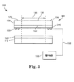
図3は、本発明の特定の一態様による抵抗性タッチセンサー300の概略側面図を示す。説明を容易にするためにかつ一般性を失わずに、図1および図2に示される層および部品のいくつかは、図3では再掲されていない。タッチセンサー300は、タッチパネル301、外部電極198、および電子機器199を含む。タッチパネル301は、タッチ感知領域195を覆うセンサー基板110、タッチ感知領域のセンサー基板110上に配設される第1検知電極120、センサー基板110に面しかつ境界領域170を覆う自立誘電体基板130、およびタッチ感知領域195の自立支持誘電体基板130上に配設される第2検知電極310を含む。タッチパネル301は、境界領域170内の自立誘電体基板130上に配設される複数の補助電極150をさらに含む。
FIG. 3 shows a schematic side view of a
本発明の一実施形態によれば、タッチ感知領域195においてタッチセンサー300に加えられるタッチ入力は、そうでなければ分離されている第1および第2検知電極を、タッチ位置で互いに物理的に接触させ、それによってタッチ信号を発生させる。補助電極150は、発生されたタッチ信号を、外部電極198を経て、電子機器199に送信する。電子機器199は、送信されたタッチ信号を用いて、タッチ位置を決定する。
According to one embodiment of the present invention, touch input applied to the
抵抗性タッチセンサー300は、4線式、5線式、または8線式抵抗性タッチセンサーであり得る。タッチパネル301は、電界(field)を線形化し、あるいは一般に、電気的に接続するための、追加の導電性電極(図3に示さず)をさらに有することができる。
図3は、第2検知電極310上に配設される複数の補助電極150を示す。補助電極150は、第2検知電極310と自立誘電体基板130との間に配設され得る。一般に、補助電極150の一部分は、誘電体基板130の第1側面131上に配設されてもよく、また補助電極150の他の部分は、誘電体基板130の第2側面132上に配設されてもよい。
FIG. 3 shows a plurality of
補助電極150は、図1〜図3に示されるように、エレクトロニクスおよび相互接続のような一般的な分野で使用される任意の適切な方法を用いて、検知電極に接続されてもよい。典型的な方法を、本発明に従って、図4および図5に図示する。
The
図4は、本発明の一実施形態によるタッチセンサー400の一部分の概略側面を図示する。タッチセンサー400は、自立誘電体基板130、境界領域170において自立誘電体基板130上に配設される複数の補助電極150、補助電極150上に配設される保護層410、および保護層410上に配設される電気シールド層420を含む。タッチセンサー400は、補助電極150に対向して、自立誘電体基板130上に配設され、誘電体基板130を、例えば検知電極(図4に示さず)に取り付けるための接着剤層(adhesive layer)430をさらに含む。タッチセンサー400は、第1ビア(via)440および第2ビア450をさらに含む。第1ビア440は、自立誘電基板130内に形成され、また第2ビア450は、接着剤層430内に形成される。ビア440および450は、補助電極150と検知電極(図4に示さず)との間を電気的に接続するために用いられる。ビア440および450は、検知電極を補助電極150に電気的に接続するために、導電材料460で充填され得る。このような積層配置は、境界(border)を減らすことができる。本発明のこの態様は、タッチセンサーを小さな境界表示装置(border display device)と一体化するのが望ましい用途において特に有用であり得る。
FIG. 4 illustrates a schematic side view of a portion of a
ビア440および450を、例えば、打ち抜き(punching)、ダイス切断(die cutting)、レーザー切断、ナイフ切断、または化学エッチングによって形成することができる。導電性材料460は、例えば、銀導電性ペースト、金導電性ペースト、パラジウム導電性ペースト、または炭素導電性ペーストなどの導電性ペーストであり得る。
接着剤層430は、紫外線硬化接着剤、感圧接着剤、エポキシ、ウレタン、チオレン、シアノアクリレート、熱活性化接着剤、熱硬化性接着剤、または自立誘電体層130を検知電極に取り付けるのに適すると考えられる任意の他の接着剤であり得る。
保護層410は、好ましくは、電気絶縁層であり、かつ一般に、例えば処理中生じることがある損傷から補助電極150を保護するために用いることができる。保護層410で用いるのに適した材料には、接着剤、ポリイミドカバーコート系(polyimide covercoat system)(感光性(photoimagable)または印刷された)、およびソルダレジストがある。
The
シールド層420は、好ましくは、高導電率を有し、かつ一般に、電気的雑音干渉などの電気的干渉から補助電極150を保護するように設計される。シールド層420は、好ましくは、補助電極150から電気的に絶縁される。図4には示さない他の層を、電気的絶縁を助けるために用いることができるが、保護層410を、シールド層420を補助電極150からを絶縁するために用いることができる。シールド層420は、金属であり得る。シールド層420で用いるのに適した金属材料には、金、銅、および銀がある。
The
図4は、一般に、境界領域170に制限される保護層410およびシールド層420を示すが、その一方または両方の層は、境界領域の外部に、例えばタッチ感知領域の中に伸びることができることが認識されよう。さらに、図4は、別個の補助電極150を続けて覆う両方の層を示すが、別個の保護層410および/または別個のシールド層420が、図5に示されるように、別個の補助電極150を覆うために用いられ得ることが認識されよう。
4 shows a
図4は、境界領域170の外部に伸びる接着剤層430を示す。一般に、接着剤層430は、境界領域およびタッチ感知領域において誘電体基板130上に配設されてよい。例えば、基板130が、タッチ感知領域に対応する開口領域を有するある用途または設計では、接着剤層430は、境界領域に制限される場合がある。
FIG. 4 shows an
図5は、本発明の他の実施形態によるタッチセンサー500の一部分の概略側面を図示する。タッチセンサー500は、自立誘電体基板130、境界領域170において自立誘電体基板130上に配設される複数の補助電極150、補助電極150上に配設される保護層410、および保護層410上に配設される電気シールド層420を含む。タッチセンサー500は、補助電極150と同じ側の、自立誘電体基板130上に配設され、自立誘電体基板を、例えば検知電極(図5に示さず)に取り付けるための接着剤層430をさらに含む。タッチセンサー500は、保護層410に形成される第1ビア510、シールド層420に形成される第2ビア520、および接着剤層430に形成される第3ビア530をさらに含む。ビア510、520、および530を、補助電極150と検知電極(図5には示さず)との間を電気的に接続するために用いることができる。
FIG. 5 illustrates a schematic side view of a portion of a
図6は、本発明の一態様によるタッチセンサーシステム600の概略断面を図示する。表示システム600は、タッチセンサー601およびディスプレー602を含む。ディスプレー602は、タッチセンサー601を通して視認可能であり得る。タッチセンサー601は、本発明の任意の実施形態によるタッチセンサーであり得る。ディスプレー602は、恒久的なまたは入れ替え可能なグラフィックス(例えば、絵、地図、アイコンなど)ならびに液晶ディスプレー(LCD)、陰極線管(CRT)、プラズマディスプレー、エレクトロルミネセンスディスプレー、OLED、電気泳動ディスプレー(electrophoretic display)などの電子ディスプレーを含むことができる。図6では、ディスプレー602およびタッチセンサー601は、2つの別個の部品として示されているが、この2つの部品を、単一のユニットに一体化することができることが認識されよう。例えば、タッチセンサー601を、ディスプレー602に積層させることができる。その代りに、タッチセンサー601は、ディスプレー602の一体部分であり得る。
FIG. 6 illustrates a schematic cross section of a
図7は、タッチセンサー720が、本発明の特定の一態様による表示装置と一体化される、典型的なタッチディスプレーシステム700の概略断面を図示する。図7は、表示基板710、アクティブディスプレー部品701、およびタッチセンサー720を示す。タッチセンサー720は、本発明の任意の態様によるタッチセンサーであり得る。タッチセンサー720は、検知電極120、自立誘電体基板130、および誘電体基板130上に配設される複数の補助電極150を含む。基板710は、タッチセンサー720のための基板としての役割りをすることができる。アクティブ部品701は、例えば、表示システムで用いることができる全ての部品を含むことがある。例えば、部品701は、液晶セル、偏光器、リターダ、バックライト、カラーフィルターなどを含むLCDディスプレーで典型的に用いられるアクティブ層およびアクティブ部品を含むことができる。ディスプレー部品701は、タッチセンサー720を通して視認可能であってよい。タッチ感知領域で可撓性ガラス層130に加えられるタッチ入力は、タッチ信号を誘導することができる。タッチ位置は、この誘導されたタッチ信号を検出することによって決定することができる。
FIG. 7 illustrates a schematic cross-section of an exemplary
上に引用した全ての特許、特許出願、およびその他の刊行物は、完全に再掲されるのと同様に、参照により本明細書に援用される。本発明の特定の例を、本発明のさまざまな態様の説明を容易にするために詳細に上述したが、本発明はこの例の詳細に限定されるものではないことを理解されたい。本発明は、むしろ、添付の特許請求の範囲によって規定されるような発明の精神および範囲に入る全ての修正、実施形態、および代替を包含するものである。 All patents, patent applications, and other publications cited above are hereby incorporated by reference as if fully reprinted. While specific examples of the invention have been described above in detail to facilitate the description of various aspects of the invention, it is to be understood that the invention is not limited to the details of this example. The invention rather is intended to encompass all modifications, embodiments, and alternatives falling within the spirit and scope of the invention as defined by the appended claims.
Claims (37)
タッチ感知領域を覆うセンサー基板であって、前記タッチ感知領域は、前記タッチセンサーの前側面から前記タッチ感知領域に加えられるタッチ入力を受けるように構成される、センサー基板と、
前記タッチ感知領域において前記センサー基板上に配設される検知電極と、
境界領域を覆う自立誘電体基板であって、前記境界領域は、前記タッチ感知領域の外部にあり、前記誘電体基板は、前記検知電極と前記タッチセンサーの前側面との間に配設される、自立誘電体基板と、
前記境界領域において前記自立誘電体基板上に配設される複数の補助電極であって、前記タッチセンサーは、該タッチセンサーの前側面から前記タッチ感知領域に加えられる前記タッチ入力に応答して、タッチ信号を前記検知電極に発生させ、前記補助電極は、前記タッチ信号を、該タッチ信号を用いてタッチ位置を決定するように構成される電子機器に送信する、補助電極と、を含むタッチセンサー。 A touch sensor,
A sensor substrate covering a touch sensing area, wherein the touch sensing area is configured to receive a touch input applied to the touch sensing area from a front side of the touch sensor;
A sensing electrode disposed on the sensor substrate in the touch sensing region;
A self-supporting dielectric substrate covering a boundary region, wherein the boundary region is outside the touch sensing region, and the dielectric substrate is disposed between the detection electrode and a front side surface of the touch sensor. A self-supporting dielectric substrate;
A plurality of auxiliary electrodes disposed on the free-standing dielectric substrate in the boundary region, wherein the touch sensor is responsive to the touch input applied to the touch sensing region from a front side surface of the touch sensor; A touch sensor that generates a touch signal on the sensing electrode, and the auxiliary electrode transmits the touch signal to an electronic device configured to determine a touch position using the touch signal. .
タッチ感知領域を覆うセンサー基板であって、前記タッチ感知領域は、該タッチ感知領域に加えられるタッチ入力を受けるように構成される、センサー基板と、
前記タッチ感知領域において前記センサー基板上に配設される検知電極と、
境界領域を覆う自立誘電体基板であって、前記境界領域は、前記タッチ感知領域の外部にある、自立誘電体基板と、
前記境界領域において前記誘電体基板上に配設される複数の補助電極であって、前記タッチセンサーは、該タッチセンサーと前記タッチ感知領域に加えられる前記タッチ入力との間の容量性カップリングに応答して、タッチ信号を発生し、前記補助電極は、前記タッチ信号を、該タッチ信号を用いてタッチ位置を決定するように構成される電子機器に送信する、補助電極と、を含む容量性タッチセンサー。 A capacitive touch sensor,
A sensor substrate covering the touch sensitive area, wherein the touch sensitive area is configured to receive a touch input applied to the touch sensitive area;
A sensing electrode disposed on the sensor substrate in the touch sensing region;
A free-standing dielectric substrate covering a boundary region, wherein the boundary region is outside the touch-sensitive region; and
A plurality of auxiliary electrodes disposed on the dielectric substrate in the boundary region, wherein the touch sensor is for capacitive coupling between the touch sensor and the touch input applied to the touch sensing region. Responsively generating a touch signal, wherein the auxiliary electrode includes an auxiliary electrode that transmits the touch signal to an electronic device configured to determine a touch position using the touch signal. Touch sensor.
Applications Claiming Priority (2)
| Application Number | Priority Date | Filing Date | Title |
|---|---|---|---|
| US10/736,388 US7339579B2 (en) | 2003-12-15 | 2003-12-15 | Wiring harness and touch sensor incorporating same |
| PCT/US2004/039495 WO2005062466A2 (en) | 2003-12-15 | 2004-11-23 | Wiring harness and touch sensor incorporating same |
Publications (2)
| Publication Number | Publication Date |
|---|---|
| JP2007514389A true JP2007514389A (en) | 2007-05-31 |
| JP2007514389A5 JP2007514389A5 (en) | 2008-01-17 |
Family
ID=34653887
Family Applications (1)
| Application Number | Title | Priority Date | Filing Date |
|---|---|---|---|
| JP2006545680A Withdrawn JP2007514389A (en) | 2003-12-15 | 2004-11-23 | Wire harness and touch sensor incorporating it |
Country Status (8)
| Country | Link |
|---|---|
| US (2) | US7339579B2 (en) |
| EP (1) | EP1697826A2 (en) |
| JP (1) | JP2007514389A (en) |
| KR (1) | KR20070006690A (en) |
| CN (1) | CN100440120C (en) |
| AU (1) | AU2004304635A1 (en) |
| TW (1) | TW200534581A (en) |
| WO (1) | WO2005062466A2 (en) |
Cited By (1)
| Publication number | Priority date | Publication date | Assignee | Title |
|---|---|---|---|---|
| JP2013514589A (en) * | 2009-12-16 | 2013-04-25 | スリーエム イノベイティブ プロパティズ カンパニー | Touch sense device with multilayer electrodes having improved optical and electrical performance |
Families Citing this family (197)
| Publication number | Priority date | Publication date | Assignee | Title |
|---|---|---|---|---|
| US7663607B2 (en) | 2004-05-06 | 2010-02-16 | Apple Inc. | Multipoint touchscreen |
| AT410844B (en) * | 2002-03-25 | 2003-08-25 | Christian Stockinger | Hand, or hand part, physiological measurement device comprises an array of sensors with which the hand or hand part is placed in contact with measurement values processed so that only sensors in complete contact are considered |
| US7339579B2 (en) * | 2003-12-15 | 2008-03-04 | 3M Innovative Properties Company | Wiring harness and touch sensor incorporating same |
| TWM269472U (en) * | 2005-01-18 | 2005-07-01 | Advanced Touch Optics Technolo | Improved touch panel |
| KR100552451B1 (en) * | 2005-07-27 | 2006-02-21 | 실리콘 디스플레이 (주) | Apparatus and method for detecting unevenness |
| US7869181B2 (en) * | 2006-03-29 | 2011-01-11 | The Boeing Company | Flex circuit lightning protection applique system for skin fasteners in composite structures |
| US8259078B2 (en) | 2006-06-09 | 2012-09-04 | Apple Inc. | Touch screen liquid crystal display |
| KR102125605B1 (en) | 2006-06-09 | 2020-06-22 | 애플 인크. | Touch screen liquid crystal display |
| CN104965621B (en) | 2006-06-09 | 2018-06-12 | 苹果公司 | Touch screen LCD and its operating method |
| US7920129B2 (en) * | 2007-01-03 | 2011-04-05 | Apple Inc. | Double-sided touch-sensitive panel with shield and drive combined layer |
| US8493330B2 (en) | 2007-01-03 | 2013-07-23 | Apple Inc. | Individual channel phase delay scheme |
| US9710095B2 (en) | 2007-01-05 | 2017-07-18 | Apple Inc. | Touch screen stack-ups |
| US20080309633A1 (en) * | 2007-06-13 | 2008-12-18 | Apple Inc. | Touch-sensitive display |
| US8633915B2 (en) | 2007-10-04 | 2014-01-21 | Apple Inc. | Single-layer touch-sensitive display |
| TW200921483A (en) * | 2007-11-09 | 2009-05-16 | Tpk Touch Solutions Inc | Touch-control display panel with an electric-field shielding layer |
| EP2073108B1 (en) * | 2007-12-19 | 2018-03-21 | EM Microelectronic-Marin SA | Screen with capacitive tactile areas |
| FR2925717B1 (en) * | 2007-12-19 | 2010-06-18 | Stantum | MULTICONTATC TRANSPARENT TOUCH SENSOR BASED ON METALLIC SURFACE DEPOSITION |
| TWI374379B (en) | 2007-12-24 | 2012-10-11 | Wintek Corp | Transparent capacitive touch panel and manufacturing method thereof |
| CN101470555A (en) * | 2007-12-25 | 2009-07-01 | 义隆电子股份有限公司 | Touch panel with function of preventing fault detection |
| US20090174676A1 (en) | 2008-01-04 | 2009-07-09 | Apple Inc. | Motion component dominance factors for motion locking of touch sensor data |
| US8723809B1 (en) * | 2008-01-18 | 2014-05-13 | Rockwell Collins, Inc. | Touch panel system and process |
| TWM348999U (en) * | 2008-02-18 | 2009-01-11 | Tpk Touch Solutions Inc | Capacitive touch panel |
| KR101727444B1 (en) * | 2008-02-28 | 2017-04-14 | 쓰리엠 이노베이티브 프로퍼티즈 컴파니 | Touch screen sensor |
| CN104090673B (en) | 2008-02-28 | 2018-02-23 | 3M创新有限公司 | Touch screen sensor with low visibility conductor |
| CN102016768B (en) | 2008-02-28 | 2014-11-19 | 3M创新有限公司 | Touch screen sensor having varying sheet resistance |
| CN102017071B (en) | 2008-02-28 | 2013-12-18 | 3M创新有限公司 | Methods of patterning conductor on substrate |
| US8284332B2 (en) * | 2008-08-01 | 2012-10-09 | 3M Innovative Properties Company | Touch screen sensor with low visibility conductors |
| US9069418B2 (en) * | 2008-06-06 | 2015-06-30 | Apple Inc. | High resistivity metal fan out |
| JP2010020730A (en) * | 2008-07-14 | 2010-01-28 | Fujitsu Component Ltd | Input detection circuit, input detection method, input detection program, and input detection apparatus |
| US8228306B2 (en) | 2008-07-23 | 2012-07-24 | Flextronics Ap, Llc | Integration design for capacitive touch panels and liquid crystal displays |
| US9128568B2 (en) | 2008-07-30 | 2015-09-08 | New Vision Display (Shenzhen) Co., Limited | Capacitive touch panel with FPC connector electrically coupled to conductive traces of face-to-face ITO pattern structure in single plane |
| US20100059294A1 (en) * | 2008-09-08 | 2010-03-11 | Apple Inc. | Bandwidth enhancement for a touch sensor panel |
| US8816967B2 (en) * | 2008-09-25 | 2014-08-26 | Apple Inc. | Capacitive sensor having electrodes arranged on the substrate and the flex circuit |
| US8209861B2 (en) | 2008-12-05 | 2012-07-03 | Flextronics Ap, Llc | Method for manufacturing a touch screen sensor assembly |
| US8274486B2 (en) | 2008-12-22 | 2012-09-25 | Flextronics Ap, Llc | Diamond pattern on a single layer |
| TWI401588B (en) * | 2008-12-26 | 2013-07-11 | Higgstec Inc | Touch panel with parallel electrode pattern |
| KR101022087B1 (en) * | 2009-01-16 | 2011-03-17 | 삼성모바일디스플레이주식회사 | Touch Screen Panel |
| KR101048930B1 (en) * | 2009-01-16 | 2011-07-12 | 삼성모바일디스플레이주식회사 | Touch screen panel |
| KR101022105B1 (en) | 2009-01-16 | 2011-03-17 | 삼성모바일디스플레이주식회사 | Touch Screen Panel and Fabricating Method for the Same |
| KR101022185B1 (en) * | 2009-01-16 | 2011-03-17 | 삼성모바일디스플레이주식회사 | Touch Screen Panel |
| US9261997B2 (en) * | 2009-02-02 | 2016-02-16 | Apple Inc. | Touch regions in diamond configuration |
| US8922521B2 (en) | 2009-02-02 | 2014-12-30 | Apple Inc. | Switching circuitry for touch sensitive display |
| JP5337061B2 (en) * | 2009-02-20 | 2013-11-06 | セイコーインスツル株式会社 | Touch panel and display device including the same |
| US8593410B2 (en) | 2009-04-10 | 2013-11-26 | Apple Inc. | Touch sensor panel design |
| JP2010267251A (en) * | 2009-04-15 | 2010-11-25 | Rohm Co Ltd | Touch-type input device and method for controlling the same |
| US8624849B2 (en) * | 2009-04-20 | 2014-01-07 | Apple Inc. | Touch actuated sensor configuration integrated with an OLED structure |
| EP2426579A4 (en) * | 2009-04-28 | 2013-01-23 | Nec Corp | Touch panel, touch panel manufactruing method, and electronic apparatus |
| EP2431845B1 (en) * | 2009-05-11 | 2017-08-02 | Kyocera Corporation | Touch panel and display device provided with same |
| TWI390280B (en) * | 2009-05-27 | 2013-03-21 | Au Optronics Corp | Touch panel display and touch display device |
| KR101667801B1 (en) * | 2009-06-19 | 2016-10-20 | 삼성전자주식회사 | Touch panel and electronic device including the touch panel |
| KR101658991B1 (en) * | 2009-06-19 | 2016-09-22 | 삼성전자주식회사 | Touch panel and electronic device including the touch panel |
| KR101389815B1 (en) * | 2009-06-24 | 2014-04-29 | 마이크로칩 테크놀로지 저머니 Ⅱ 게엠베하 운트 콤파니 카게 | Electrode arrangement for display device |
| US8957874B2 (en) * | 2009-06-29 | 2015-02-17 | Apple Inc. | Touch sensor panel design |
| JP5300640B2 (en) | 2009-07-27 | 2013-09-25 | 株式会社ジャパンディスプレイウェスト | Capacitance type input device and electro-optical device with input device |
| TWM380535U (en) * | 2009-12-03 | 2010-05-11 | Transtouch Technology Inc | Capacitive touch panel |
| US20110134050A1 (en) * | 2009-12-07 | 2011-06-09 | Harley Jonah A | Fabrication of touch sensor panel using laser ablation |
| KR101616875B1 (en) * | 2010-01-07 | 2016-05-02 | 삼성전자주식회사 | Touch panel and electronic device including the touch panel |
| KR101631892B1 (en) * | 2010-01-28 | 2016-06-21 | 삼성전자주식회사 | Touch panel and electronic device including the touch panel |
| TWI381303B (en) | 2010-02-09 | 2013-01-01 | Oji Paper Co | Conductive laminate and touch panel made there of |
| TW201203041A (en) | 2010-03-05 | 2012-01-16 | Canatu Oy | A touch sensitive film and a touch sensing device |
| FI125151B (en) * | 2010-03-05 | 2015-06-15 | Canatu Oy | Process for making a conformal element |
| TW201145132A (en) * | 2010-03-11 | 2011-12-16 | Alps Electric Co Ltd | Translucent inputting device |
| KR101710523B1 (en) * | 2010-03-22 | 2017-02-27 | 삼성전자주식회사 | Touch panel and electronic device including the touch panel |
| KR101055510B1 (en) * | 2010-03-26 | 2011-08-08 | 삼성전기주식회사 | Touch panel |
| US9285929B2 (en) | 2010-03-30 | 2016-03-15 | New Vision Display (Shenzhen) Co., Limited | Touchscreen system with simplified mechanical touchscreen design using capacitance and acoustic sensing technologies, and method therefor |
| KR101661728B1 (en) | 2010-05-11 | 2016-10-04 | 삼성전자주식회사 | User's input apparatus and electronic device including the user's input apparatus |
| US8283800B2 (en) | 2010-05-27 | 2012-10-09 | Ford Global Technologies, Llc | Vehicle control system with proximity switch and method thereof |
| KR20110133359A (en) * | 2010-06-04 | 2011-12-12 | 삼성전기주식회사 | Capacitive type touch panel |
| CN104714696B (en) * | 2010-07-08 | 2017-11-24 | 友达光电股份有限公司 | touch display substrate |
| KR20120010795A (en) * | 2010-07-27 | 2012-02-06 | 삼성전기주식회사 | Electronic paper associated with touch panel |
| US9652088B2 (en) | 2010-07-30 | 2017-05-16 | Apple Inc. | Fabrication of touch sensor panel using laser ablation |
| US8575949B2 (en) | 2010-08-25 | 2013-11-05 | Ford Global Technologies, Llc | Proximity sensor with enhanced activation |
| US8454181B2 (en) | 2010-08-25 | 2013-06-04 | Ford Global Technologies, Llc | Light bar proximity switch |
| KR20120030832A (en) * | 2010-09-20 | 2012-03-29 | 삼성전기주식회사 | Touch screen and method of manufacturing the same |
| KR101809191B1 (en) * | 2010-10-11 | 2018-01-18 | 삼성전자주식회사 | Touch panel |
| JP2012084025A (en) * | 2010-10-14 | 2012-04-26 | Hitachi Displays Ltd | Display device with touch panel |
| US10185446B2 (en) * | 2010-10-15 | 2019-01-22 | Apple Inc. | Touch sensor arrays with integrated inter-layer contacts |
| US9491852B2 (en) | 2010-10-15 | 2016-11-08 | Apple Inc. | Trace border routing |
| CN101976164B (en) * | 2010-10-18 | 2013-06-05 | 汕头超声显示器有限公司 | Capacitor touch screen |
| US8808483B2 (en) * | 2010-11-05 | 2014-08-19 | Apple Inc. | Method of making a curved touch panel |
| US9652089B2 (en) * | 2010-11-09 | 2017-05-16 | Tpk Touch Solutions Inc. | Touch panel stackup |
| US9563315B2 (en) | 2010-11-09 | 2017-02-07 | Tpk Touch Solutions Inc. | Capacitive touch panel and method for producing the same |
| EP3026534A1 (en) | 2010-11-09 | 2016-06-01 | TPK Touch Solutions Inc. | Touch panel device |
| KR101735715B1 (en) | 2010-11-23 | 2017-05-15 | 삼성전자주식회사 | Input sensing circuit and touch panel including the input sensing circuit |
| FR2968488B1 (en) | 2010-12-01 | 2012-12-21 | St Microelectronics Rousset | METHOD FOR CONTROLLING A CAPACITIVE TOUCH SURFACE |
| FR2968421B1 (en) | 2010-12-01 | 2013-04-05 | St Microelectronics Rousset | CAPACITIVE TOUCH SURFACE CONFIGURED TO MAKE PROXIMITY DETECTION |
| FR2968487B1 (en) * | 2010-12-01 | 2012-12-21 | St Microelectronics Rousset | DIRECTIONAL DETECTION DEVICE FOR CAPACITIVE PROXIMITY |
| US8804056B2 (en) | 2010-12-22 | 2014-08-12 | Apple Inc. | Integrated touch screens |
| US9866660B2 (en) * | 2011-03-21 | 2018-01-09 | Apple Inc. | Electronic devices with concave displays |
| TWI520040B (en) | 2011-04-08 | 2016-02-01 | Elan Microelectronics Corp | Capacitive touch panel with improved environmental impact and its application |
| KR101784436B1 (en) | 2011-04-18 | 2017-10-11 | 삼성전자주식회사 | Touch panel and driving device for the touch panel |
| US8975903B2 (en) | 2011-06-09 | 2015-03-10 | Ford Global Technologies, Llc | Proximity switch having learned sensitivity and method therefor |
| TWI447978B (en) | 2011-06-09 | 2014-08-01 | Shih Hua Technology Ltd | Method for making touch panel |
| TWI425562B (en) | 2011-06-09 | 2014-02-01 | Shih Hua Technology Ltd | Method for making touch panel |
| TWI512555B (en) | 2011-06-09 | 2015-12-11 | Shih Hua Technology Ltd | Touch panel and method for making the same |
| US8928336B2 (en) | 2011-06-09 | 2015-01-06 | Ford Global Technologies, Llc | Proximity switch having sensitivity control and method therefor |
| TWI428667B (en) | 2011-06-09 | 2014-03-01 | Shih Hua Technology Ltd | Method for making touch panel |
| TWI457808B (en) * | 2011-06-09 | 2014-10-21 | Shih Hua Technology Ltd | Touch screen |
| FR2976688B1 (en) | 2011-06-16 | 2021-04-23 | Nanotec Solution | DEVICE AND METHOD FOR GENERATING AN ELECTRICAL POWER SUPPLY IN AN ELECTRONIC SYSTEM WITH A VARIABLE REFERENCE POTENTIAL. |
| US10004286B2 (en) | 2011-08-08 | 2018-06-26 | Ford Global Technologies, Llc | Glove having conductive ink and method of interacting with proximity sensor |
| US9143126B2 (en) | 2011-09-22 | 2015-09-22 | Ford Global Technologies, Llc | Proximity switch having lockout control for controlling movable panel |
| CN103049121B (en) * | 2011-10-13 | 2016-04-06 | 宸鸿科技(厦门)有限公司 | Contactor control device and manufacture method thereof |
| CN103076907B (en) * | 2011-10-26 | 2016-04-06 | 宸鸿科技(厦门)有限公司 | Contactor control device and manufacture method thereof |
| US10112556B2 (en) | 2011-11-03 | 2018-10-30 | Ford Global Technologies, Llc | Proximity switch having wrong touch adaptive learning and method |
| US8994228B2 (en) | 2011-11-03 | 2015-03-31 | Ford Global Technologies, Llc | Proximity switch having wrong touch feedback |
| US8878438B2 (en) | 2011-11-04 | 2014-11-04 | Ford Global Technologies, Llc | Lamp and proximity switch assembly and method |
| FR2985049B1 (en) | 2011-12-22 | 2014-01-31 | Nanotec Solution | CAPACITIVE MEASURING DEVICE WITH SWITCHED ELECTRODES FOR TOUCHLESS CONTACTLESS INTERFACES |
| CN104169850B (en) | 2012-01-12 | 2017-06-06 | 辛纳普蒂克斯公司 | Individual layer capacitive character imaging sensor |
| US8525955B2 (en) | 2012-01-31 | 2013-09-03 | Multek Display (Hong Kong) Limited | Heater for liquid crystal display |
| LU91942B1 (en) * | 2012-02-10 | 2013-08-12 | Iee Sarl | Capacitive detection device |
| US9013425B2 (en) | 2012-02-23 | 2015-04-21 | Cypress Semiconductor Corporation | Method and apparatus for data transmission via capacitance sensing device |
| US9944237B2 (en) | 2012-04-11 | 2018-04-17 | Ford Global Technologies, Llc | Proximity switch assembly with signal drift rejection and method |
| US9531379B2 (en) | 2012-04-11 | 2016-12-27 | Ford Global Technologies, Llc | Proximity switch assembly having groove between adjacent proximity sensors |
| US9184745B2 (en) | 2012-04-11 | 2015-11-10 | Ford Global Technologies, Llc | Proximity switch assembly and method of sensing user input based on signal rate of change |
| US9660644B2 (en) | 2012-04-11 | 2017-05-23 | Ford Global Technologies, Llc | Proximity switch assembly and activation method |
| US9559688B2 (en) | 2012-04-11 | 2017-01-31 | Ford Global Technologies, Llc | Proximity switch assembly having pliable surface and depression |
| US9197206B2 (en) | 2012-04-11 | 2015-11-24 | Ford Global Technologies, Llc | Proximity switch having differential contact surface |
| US9520875B2 (en) | 2012-04-11 | 2016-12-13 | Ford Global Technologies, Llc | Pliable proximity switch assembly and activation method |
| US9287864B2 (en) | 2012-04-11 | 2016-03-15 | Ford Global Technologies, Llc | Proximity switch assembly and calibration method therefor |
| US9831870B2 (en) | 2012-04-11 | 2017-11-28 | Ford Global Technologies, Llc | Proximity switch assembly and method of tuning same |
| US9568527B2 (en) | 2012-04-11 | 2017-02-14 | Ford Global Technologies, Llc | Proximity switch assembly and activation method having virtual button mode |
| US8933708B2 (en) | 2012-04-11 | 2015-01-13 | Ford Global Technologies, Llc | Proximity switch assembly and activation method with exploration mode |
| US9219472B2 (en) | 2012-04-11 | 2015-12-22 | Ford Global Technologies, Llc | Proximity switch assembly and activation method using rate monitoring |
| US9065447B2 (en) | 2012-04-11 | 2015-06-23 | Ford Global Technologies, Llc | Proximity switch assembly and method having adaptive time delay |
| US9329723B2 (en) | 2012-04-16 | 2016-05-03 | Apple Inc. | Reconstruction of original touch image from differential touch image |
| CN103425303B (en) * | 2012-05-16 | 2016-10-05 | 宸鸿科技(厦门)有限公司 | Contact panel and the touch control display device of application thereof |
| US9136840B2 (en) | 2012-05-17 | 2015-09-15 | Ford Global Technologies, Llc | Proximity switch assembly having dynamic tuned threshold |
| US8981602B2 (en) | 2012-05-29 | 2015-03-17 | Ford Global Technologies, Llc | Proximity switch assembly having non-switch contact and method |
| US9337832B2 (en) | 2012-06-06 | 2016-05-10 | Ford Global Technologies, Llc | Proximity switch and method of adjusting sensitivity therefor |
| US9641172B2 (en) | 2012-06-27 | 2017-05-02 | Ford Global Technologies, Llc | Proximity switch assembly having varying size electrode fingers |
| JP5224203B1 (en) | 2012-07-11 | 2013-07-03 | 大日本印刷株式会社 | Touch panel sensor, touch panel device, and display device |
| US20140065400A1 (en) * | 2012-08-29 | 2014-03-06 | Eastman Chemical Company | Electrically conductive polymer compositions and films |
| US8922340B2 (en) | 2012-09-11 | 2014-12-30 | Ford Global Technologies, Llc | Proximity switch based door latch release |
| US8796575B2 (en) | 2012-10-31 | 2014-08-05 | Ford Global Technologies, Llc | Proximity switch assembly having ground layer |
| CN103838415A (en) * | 2012-11-24 | 2014-06-04 | 宝宸(厦门)光学科技有限公司 | Flexible touch panel structure and manufacture method thereof |
| US9250753B2 (en) | 2013-01-07 | 2016-02-02 | Microsoft Technology Licensing, Llc | Capacitive touch surface in close proximity to display |
| CN104007862B (en) * | 2013-02-26 | 2016-12-28 | 宏碁股份有限公司 | Contact panel |
| US9304636B2 (en) * | 2013-09-20 | 2016-04-05 | Eastman Kodak Company | Micro-wire touch screen with unpatterned conductive layer |
| US9311204B2 (en) | 2013-03-13 | 2016-04-12 | Ford Global Technologies, Llc | Proximity interface development system having replicator and method |
| CN103294312B (en) * | 2013-05-15 | 2016-04-20 | 京东方科技集团股份有限公司 | Capacitive touch screen, capacitive touch screen preparation method and display device |
| TW201445621A (en) | 2013-05-24 | 2014-12-01 | Wintek Corp | Touch-sensing electrode structure and touch-sensitive device |
| PT106994A (en) | 2013-06-09 | 2014-12-09 | Active Space Technologies Actividades Aeroespaciais Lda | METHOD AND MONITORING SYSTEM FOR AGING ELECTRIC WIRING |
| CN103324346A (en) * | 2013-06-11 | 2013-09-25 | 业成光电(深圳)有限公司 | Touch device and touch panel thereof |
| US9715314B2 (en) | 2013-06-24 | 2017-07-25 | Microsoft Technology Licensing, Llc | Capacitive touch sensor having pseudo jumpers |
| US9377646B2 (en) | 2013-06-24 | 2016-06-28 | Microsoft Technology Licensing, Llc | Capacitive touch sensor having oblique electrode matrix |
| US9552089B2 (en) | 2013-08-07 | 2017-01-24 | Synaptics Incorporated | Capacitive sensing using a matrix electrode pattern |
| US9886141B2 (en) | 2013-08-16 | 2018-02-06 | Apple Inc. | Mutual and self capacitance touch measurements in touch panel |
| US20150091842A1 (en) | 2013-09-30 | 2015-04-02 | Synaptics Incorporated | Matrix sensor for image touch sensing |
| US9298325B2 (en) | 2013-09-30 | 2016-03-29 | Synaptics Incorporated | Processing system for a capacitive sensing device |
| US10042489B2 (en) | 2013-09-30 | 2018-08-07 | Synaptics Incorporated | Matrix sensor for image touch sensing |
| US9459367B2 (en) | 2013-10-02 | 2016-10-04 | Synaptics Incorporated | Capacitive sensor driving technique that enables hybrid sensing or equalization |
| US9274662B2 (en) | 2013-10-18 | 2016-03-01 | Synaptics Incorporated | Sensor matrix pad for performing multiple capacitive sensing techniques |
| US9495046B2 (en) | 2013-10-23 | 2016-11-15 | Synaptics Incorporated | Parasitic capacitance filter for single-layer capacitive imaging sensors |
| US9081457B2 (en) | 2013-10-30 | 2015-07-14 | Synaptics Incorporated | Single-layer muti-touch capacitive imaging sensor |
| US20150199048A1 (en) * | 2014-01-15 | 2015-07-16 | Carestream Health, Inc. | Touch panel assembly |
| KR102183655B1 (en) * | 2014-01-28 | 2020-11-27 | 삼성디스플레이 주식회사 | Display apparatus |
| CN103809828B (en) * | 2014-02-25 | 2017-06-16 | 福建科创光电有限公司 | Narrow frame one chip capacitance induction touch panel of double color layers and preparation method thereof |
| US9798429B2 (en) | 2014-02-28 | 2017-10-24 | Synaptics Incorporated | Guard electrodes in a sensing stack |
| US10133421B2 (en) | 2014-04-02 | 2018-11-20 | Synaptics Incorporated | Display stackups for matrix sensor |
| US9927832B2 (en) | 2014-04-25 | 2018-03-27 | Synaptics Incorporated | Input device having a reduced border region |
| US9690397B2 (en) | 2014-05-20 | 2017-06-27 | Synaptics Incorporated | System and method for detecting an active pen with a matrix sensor |
| WO2015178920A1 (en) | 2014-05-22 | 2015-11-26 | Onamp Research Llc | Panel bootstrapping architectures for in-cell self-capacitance |
| US10289251B2 (en) | 2014-06-27 | 2019-05-14 | Apple Inc. | Reducing floating ground effects in pixelated self-capacitance touch screens |
| JP2017524203A (en) * | 2014-08-11 | 2017-08-24 | スリーエム イノベイティブ プロパティズ カンパニー | Capacitive touch sensor device |
| US20160054825A1 (en) * | 2014-08-25 | 2016-02-25 | Carestream Health, Inc. | Touch panels and methods |
| US9880655B2 (en) | 2014-09-02 | 2018-01-30 | Apple Inc. | Method of disambiguating water from a finger touch on a touch sensor panel |
| US10705658B2 (en) | 2014-09-22 | 2020-07-07 | Apple Inc. | Ungrounded user signal compensation for pixelated self-capacitance touch sensor panel |
| US10038443B2 (en) | 2014-10-20 | 2018-07-31 | Ford Global Technologies, Llc | Directional proximity switch assembly |
| US10712867B2 (en) | 2014-10-27 | 2020-07-14 | Apple Inc. | Pixelated self-capacitance water rejection |
| TWI537795B (en) * | 2014-11-26 | 2016-06-11 | 林志忠 | Touch panel structure |
| US10175827B2 (en) | 2014-12-23 | 2019-01-08 | Synaptics Incorporated | Detecting an active pen using a capacitive sensing device |
| US9778713B2 (en) | 2015-01-05 | 2017-10-03 | Synaptics Incorporated | Modulating a reference voltage to preform capacitive sensing |
| CN104615318A (en) * | 2015-01-23 | 2015-05-13 | 深圳市华星光电技术有限公司 | Touch screen and terminal provided with same |
| WO2016126525A1 (en) | 2015-02-02 | 2016-08-11 | Apple Inc. | Flexible self-capacitance and mutual capacitance touch sensing system architecture |
| US10488992B2 (en) | 2015-03-10 | 2019-11-26 | Apple Inc. | Multi-chip touch architecture for scalability |
| US9654103B2 (en) | 2015-03-18 | 2017-05-16 | Ford Global Technologies, Llc | Proximity switch assembly having haptic feedback and method |
| JP2016180747A (en) * | 2015-03-24 | 2016-10-13 | パナソニックIpマネジメント株式会社 | Pressure sensor |
| US9939972B2 (en) | 2015-04-06 | 2018-04-10 | Synaptics Incorporated | Matrix sensor with via routing |
| US9548733B2 (en) | 2015-05-20 | 2017-01-17 | Ford Global Technologies, Llc | Proximity sensor assembly having interleaved electrode configuration |
| US9715304B2 (en) | 2015-06-30 | 2017-07-25 | Synaptics Incorporated | Regular via pattern for sensor-based input device |
| US10095948B2 (en) | 2015-06-30 | 2018-10-09 | Synaptics Incorporated | Modulation scheme for fingerprint sensing |
| US9720541B2 (en) | 2015-06-30 | 2017-08-01 | Synaptics Incorporated | Arrangement of sensor pads and display driver pads for input device |
| CN205028263U (en) | 2015-09-07 | 2016-02-10 | 辛纳普蒂克斯公司 | Capacitance sensor |
| US10037112B2 (en) | 2015-09-30 | 2018-07-31 | Synaptics Incorporated | Sensing an active device'S transmission using timing interleaved with display updates |
| US10365773B2 (en) | 2015-09-30 | 2019-07-30 | Apple Inc. | Flexible scan plan using coarse mutual capacitance and fully-guarded measurements |
| US10386940B2 (en) * | 2015-10-30 | 2019-08-20 | Microsoft Technology Licensing, Llc | Touch sensing of user input device |
| US10120509B2 (en) * | 2015-12-29 | 2018-11-06 | Stmicroelectronics Asia Pacific Pte Ltd | Common mode noise reduction in capacitive touch sensing |
| US10067587B2 (en) | 2015-12-29 | 2018-09-04 | Synaptics Incorporated | Routing conductors in an integrated display device and sensing device |
| CN106933400B (en) | 2015-12-31 | 2021-10-29 | 辛纳普蒂克斯公司 | Single layer sensor pattern and sensing method |
| EP3417024B1 (en) | 2016-02-19 | 2020-08-05 | Avery Dennison Corporation | Two stage methods for processing adhesives and related compositions |
| CN106354323A (en) * | 2016-09-05 | 2017-01-25 | 京东方科技集团股份有限公司 | Substrate, manufacturing method thereof, display device and touch control device |
| AU2017208277B2 (en) | 2016-09-06 | 2018-12-20 | Apple Inc. | Back of cover touch sensors |
| WO2018081268A1 (en) | 2016-10-25 | 2018-05-03 | Avery Dennison Corporation | Block polymers with photoinitiator groups in backbone and their use in adhesive compositions |
| US10386965B2 (en) | 2017-04-20 | 2019-08-20 | Apple Inc. | Finger tracking in wet environment |
| CN107359274A (en) * | 2017-06-27 | 2017-11-17 | 上海天马有机发光显示技术有限公司 | The preparation method of display panel, display device and display panel |
| US11157109B1 (en) | 2019-09-06 | 2021-10-26 | Apple Inc. | Touch sensing with water rejection |
| US11662867B1 (en) | 2020-05-30 | 2023-05-30 | Apple Inc. | Hover detection on a touch sensor panel |
Family Cites Families (40)
| Publication number | Priority date | Publication date | Assignee | Title |
|---|---|---|---|---|
| US4198539A (en) * | 1977-01-19 | 1980-04-15 | Peptek, Inc. | System for producing electric field with predetermined characteristics and edge terminations for resistance planes therefor |
| US4371746A (en) * | 1978-01-05 | 1983-02-01 | Peptek, Incorporated | Edge terminations for impedance planes |
| US4293734A (en) * | 1979-02-23 | 1981-10-06 | Peptek, Incorporated | Touch panel system and method |
| US4353552A (en) | 1979-02-23 | 1982-10-12 | Peptek, Incorporated | Touch panel system and method |
| US4622437A (en) | 1984-11-29 | 1986-11-11 | Interaction Systems, Inc. | Method and apparatus for improved electronic touch mapping |
| US4661655B1 (en) | 1984-12-24 | 1997-01-21 | Elographics Inc | Electrographic touch sensor and method of reducing bowed equipotential fields therein |
| US4822957B1 (en) * | 1984-12-24 | 1996-11-19 | Elographics Inc | Electrographic touch sensor having reduced bow of equipotential field lines therein |
| US4797514A (en) | 1986-06-09 | 1989-01-10 | Elographics, Inc. | Touch sensitive device with increased linearity |
| US5045644A (en) | 1990-04-16 | 1991-09-03 | Elographics, Inc. | Touch sensitive screen with improved corner response |
| US5221854A (en) | 1991-11-18 | 1993-06-22 | United Solar Systems Corporation | Protective layer for the back reflector of a photovoltaic device |
| JPH05324203A (en) | 1992-05-22 | 1993-12-07 | Fujitsu Ltd | Electrostatic capacity type touch panel |
| US5451724A (en) | 1992-08-05 | 1995-09-19 | Fujitsu Limited | Touch panel for detecting a coordinate of an arbitrary position where pressure is applied |
| US5457289A (en) * | 1994-03-16 | 1995-10-10 | Microtouch Systems, Inc. | Frontally shielded capacitive touch sensor system |
| US5725957A (en) | 1994-07-29 | 1998-03-10 | Donnelly Corporation | Transparent substrate with diffuser surface |
| US6001486A (en) | 1994-07-29 | 1999-12-14 | Donnelly Corporation | Transparent substrate with diffuser surface |
| US5594222A (en) * | 1994-10-25 | 1997-01-14 | Integrated Controls | Touch sensor and control circuit therefor |
| GB9422911D0 (en) | 1994-11-14 | 1995-01-04 | Moonstone Technology Ltd | Capacitive touch detectors |
| US5650597A (en) * | 1995-01-20 | 1997-07-22 | Dynapro Systems, Inc. | Capacitive touch sensor |
| US5886687A (en) * | 1997-02-20 | 1999-03-23 | Gibson; William A. | Touch panel system utilizing capacitively-coupled electrodes |
| US6549193B1 (en) * | 1998-10-09 | 2003-04-15 | 3M Innovative Properties Company | Touch panel with improved linear response and minimal border width electrode pattern |
| JP4307635B2 (en) | 1999-06-22 | 2009-08-05 | 株式会社半導体エネルギー研究所 | Method for manufacturing semiconductor device |
| JP2001075075A (en) * | 1999-06-29 | 2001-03-23 | Seiko Epson Corp | Liquid crystal device and electronic apparatus |
| US6426245B1 (en) | 1999-07-09 | 2002-07-30 | Semiconductor Energy Laboratory Co., Ltd. | Method for manufacturing a semiconductor device |
| US6664950B1 (en) | 1999-11-17 | 2003-12-16 | L-3 Communications | Resistive touch panel using removable, tensioned top layer |
| US6305073B1 (en) * | 1999-12-29 | 2001-10-23 | Gm Nameplate, Inc. | One-sided electrode arrangement on an intermediate spacer for a touchscreen |
| US6727895B2 (en) * | 2000-02-02 | 2004-04-27 | 3M Innovative Properties Company | Touch screen panel with integral wiring traces |
| US6373618B1 (en) | 2000-05-04 | 2002-04-16 | Schott-Donnelly, Llc | Chromogenic glazing for automobiles and display filters |
| EP1297380B1 (en) | 2000-05-04 | 2008-11-26 | Schott Donnelly LLC | Method of making an electrochromic panel |
| EP1172831B1 (en) | 2000-07-12 | 2012-10-24 | Agfa-Gevaert N.V. | Switch with at least one flexible conductive member |
| US6406758B1 (en) | 2000-07-25 | 2002-06-18 | 3M Innovative Properties Company | Method of applying a protective coating to a touch screen panel |
| US6593916B1 (en) | 2000-11-03 | 2003-07-15 | James L. Aroyan | Touchscreen having multiple parallel connections to each electrode in a series resistor chain on the periphery of the touch area |
| US6583440B2 (en) | 2000-11-30 | 2003-06-24 | Seiko Epson Corporation | Soi substrate, element substrate, semiconductor device, electro-optical apparatus, electronic equipment, method of manufacturing the soi substrate, method of manufacturing the element substrate, and method of manufacturing the electro-optical apparatus |
| GB2373581B (en) | 2001-03-20 | 2004-11-10 | Eturbotouch Technology Inc | Touch screen capable of isolating noise signals |
| US6819316B2 (en) | 2001-04-17 | 2004-11-16 | 3M Innovative Properties Company | Flexible capacitive touch sensor |
| TW579019U (en) * | 2001-06-13 | 2004-03-01 | Eturbotouch Technology Inc | Flexible current type touch film |
| US6488981B1 (en) | 2001-06-20 | 2002-12-03 | 3M Innovative Properties Company | Method of manufacturing a touch screen panel |
| US20030067447A1 (en) * | 2001-07-09 | 2003-04-10 | Geaghan Bernard O. | Touch screen with selective touch sources |
| CA2494353A1 (en) * | 2002-08-02 | 2004-02-12 | Cirque Corporation | Single-layer touchpad having touch zones |
| JP2004145092A (en) | 2002-10-25 | 2004-05-20 | Seiko Epson Corp | Device and its manufacturing method, and electronic equipment with the device |
| US7339579B2 (en) * | 2003-12-15 | 2008-03-04 | 3M Innovative Properties Company | Wiring harness and touch sensor incorporating same |
-
2003
- 2003-12-15 US US10/736,388 patent/US7339579B2/en not_active Expired - Fee Related
-
2004
- 2004-11-23 EP EP04812087A patent/EP1697826A2/en not_active Ceased
- 2004-11-23 JP JP2006545680A patent/JP2007514389A/en not_active Withdrawn
- 2004-11-23 KR KR1020067014157A patent/KR20070006690A/en not_active Application Discontinuation
- 2004-11-23 AU AU2004304635A patent/AU2004304635A1/en not_active Abandoned
- 2004-11-23 CN CNB2004800409713A patent/CN100440120C/en not_active Expired - Fee Related
- 2004-11-23 WO PCT/US2004/039495 patent/WO2005062466A2/en active Application Filing
- 2004-12-07 TW TW093137826A patent/TW200534581A/en unknown
-
2007
- 2007-10-08 US US11/868,741 patent/US8194044B2/en not_active Expired - Fee Related
Cited By (1)
| Publication number | Priority date | Publication date | Assignee | Title |
|---|---|---|---|---|
| JP2013514589A (en) * | 2009-12-16 | 2013-04-25 | スリーエム イノベイティブ プロパティズ カンパニー | Touch sense device with multilayer electrodes having improved optical and electrical performance |
Also Published As
| Publication number | Publication date |
|---|---|
| CN100440120C (en) | 2008-12-03 |
| US20050126831A1 (en) | 2005-06-16 |
| US20080024461A1 (en) | 2008-01-31 |
| US7339579B2 (en) | 2008-03-04 |
| WO2005062466A3 (en) | 2005-08-25 |
| CN1918538A (en) | 2007-02-21 |
| EP1697826A2 (en) | 2006-09-06 |
| TW200534581A (en) | 2005-10-16 |
| WO2005062466A2 (en) | 2005-07-07 |
| AU2004304635A1 (en) | 2005-07-07 |
| KR20070006690A (en) | 2007-01-11 |
| US8194044B2 (en) | 2012-06-05 |
Similar Documents
| Publication | Publication Date | Title |
|---|---|---|
| US8194044B2 (en) | Wiring harness and touch sensor incorporating same | |
| US11182000B2 (en) | Smartphone | |
| US9898132B2 (en) | Electrode sheet and touch input device | |
| US9547388B2 (en) | Touch input device | |
| US20050073507A1 (en) | Touch input sensing device | |
| KR20140082367A (en) | Touch display device | |
| CN107957815B (en) | Touch control display panel | |
| KR20160096267A (en) | Touch screen pannel and manufacturing method thereof | |
| US20110227869A1 (en) | Bistable display device | |
| US20100039407A1 (en) | Sensory structure of capacitive touch panel with predetermined sensing areas | |
| KR20160095314A (en) | Touch screen panel | |
| KR20170014424A (en) | Touch sensor and image displaying device including the same | |
| US9532450B2 (en) | Lowering the sheet resistance of a conductive layer | |
| EP2735949A2 (en) | Touch panel | |
| JP7321112B2 (en) | Touch panel and display device provided with the same | |
| KR101748173B1 (en) | Touch detecting apparatus | |
| KR20160003406A (en) | Touch panel | |
| KR20150104851A (en) | Touch panel and display device | |
| KR20160003405A (en) | Touch panel |
Legal Events
| Date | Code | Title | Description |
|---|---|---|---|
| A521 | Written amendment |
Free format text: JAPANESE INTERMEDIATE CODE: A523 Effective date: 20071122 |
|
| A621 | Written request for application examination |
Free format text: JAPANESE INTERMEDIATE CODE: A621 Effective date: 20071122 |
|
| A761 | Written withdrawal of application |
Free format text: JAPANESE INTERMEDIATE CODE: A761 Effective date: 20080522 |