CN102017071B - Methods of patterning conductor on substrate - Google Patents
Methods of patterning conductor on substrate Download PDFInfo
- Publication number
- CN102017071B CN102017071B CN2009801150751A CN200980115075A CN102017071B CN 102017071 B CN102017071 B CN 102017071B CN 2009801150751 A CN2009801150751 A CN 2009801150751A CN 200980115075 A CN200980115075 A CN 200980115075A CN 102017071 B CN102017071 B CN 102017071B
- Authority
- CN
- China
- Prior art keywords
- pattern
- pressing mold
- inking
- protruding features
- protruding
- Prior art date
- Legal status (The legal status is an assumption and is not a legal conclusion. Google has not performed a legal analysis and makes no representation as to the accuracy of the status listed.)
- Expired - Fee Related
Links
Images


Classifications
-
- H—ELECTRICITY
- H05—ELECTRIC TECHNIQUES NOT OTHERWISE PROVIDED FOR
- H05K—PRINTED CIRCUITS; CASINGS OR CONSTRUCTIONAL DETAILS OF ELECTRIC APPARATUS; MANUFACTURE OF ASSEMBLAGES OF ELECTRICAL COMPONENTS
- H05K3/00—Apparatus or processes for manufacturing printed circuits
- H05K3/02—Apparatus or processes for manufacturing printed circuits in which the conductive material is applied to the surface of the insulating support and is thereafter removed from such areas of the surface which are not intended for current conducting or shielding
- H05K3/06—Apparatus or processes for manufacturing printed circuits in which the conductive material is applied to the surface of the insulating support and is thereafter removed from such areas of the surface which are not intended for current conducting or shielding the conductive material being removed chemically or electrolytically, e.g. by photo-etch process
- H05K3/061—Etching masks
-
- B—PERFORMING OPERATIONS; TRANSPORTING
- B41—PRINTING; LINING MACHINES; TYPEWRITERS; STAMPS
- B41M—PRINTING, DUPLICATING, MARKING, OR COPYING PROCESSES; COLOUR PRINTING
- B41M5/00—Duplicating or marking methods; Sheet materials for use therein
- B41M5/50—Recording sheets characterised by the coating used to improve ink, dye or pigment receptivity, e.g. for ink-jet or thermal dye transfer recording
- B41M5/52—Macromolecular coatings
-
- B—PERFORMING OPERATIONS; TRANSPORTING
- B82—NANOTECHNOLOGY
- B82Y—SPECIFIC USES OR APPLICATIONS OF NANOSTRUCTURES; MEASUREMENT OR ANALYSIS OF NANOSTRUCTURES; MANUFACTURE OR TREATMENT OF NANOSTRUCTURES
- B82Y10/00—Nanotechnology for information processing, storage or transmission, e.g. quantum computing or single electron logic
-
- B—PERFORMING OPERATIONS; TRANSPORTING
- B82—NANOTECHNOLOGY
- B82Y—SPECIFIC USES OR APPLICATIONS OF NANOSTRUCTURES; MEASUREMENT OR ANALYSIS OF NANOSTRUCTURES; MANUFACTURE OR TREATMENT OF NANOSTRUCTURES
- B82Y40/00—Manufacture or treatment of nanostructures
-
- C—CHEMISTRY; METALLURGY
- C23—COATING METALLIC MATERIAL; COATING MATERIAL WITH METALLIC MATERIAL; CHEMICAL SURFACE TREATMENT; DIFFUSION TREATMENT OF METALLIC MATERIAL; COATING BY VACUUM EVAPORATION, BY SPUTTERING, BY ION IMPLANTATION OR BY CHEMICAL VAPOUR DEPOSITION, IN GENERAL; INHIBITING CORROSION OF METALLIC MATERIAL OR INCRUSTATION IN GENERAL
- C23F—NON-MECHANICAL REMOVAL OF METALLIC MATERIAL FROM SURFACE; INHIBITING CORROSION OF METALLIC MATERIAL OR INCRUSTATION IN GENERAL; MULTI-STEP PROCESSES FOR SURFACE TREATMENT OF METALLIC MATERIAL INVOLVING AT LEAST ONE PROCESS PROVIDED FOR IN CLASS C23 AND AT LEAST ONE PROCESS COVERED BY SUBCLASS C21D OR C22F OR CLASS C25
- C23F1/00—Etching metallic material by chemical means
- C23F1/02—Local etching
-
- C—CHEMISTRY; METALLURGY
- C23—COATING METALLIC MATERIAL; COATING MATERIAL WITH METALLIC MATERIAL; CHEMICAL SURFACE TREATMENT; DIFFUSION TREATMENT OF METALLIC MATERIAL; COATING BY VACUUM EVAPORATION, BY SPUTTERING, BY ION IMPLANTATION OR BY CHEMICAL VAPOUR DEPOSITION, IN GENERAL; INHIBITING CORROSION OF METALLIC MATERIAL OR INCRUSTATION IN GENERAL
- C23F—NON-MECHANICAL REMOVAL OF METALLIC MATERIAL FROM SURFACE; INHIBITING CORROSION OF METALLIC MATERIAL OR INCRUSTATION IN GENERAL; MULTI-STEP PROCESSES FOR SURFACE TREATMENT OF METALLIC MATERIAL INVOLVING AT LEAST ONE PROCESS PROVIDED FOR IN CLASS C23 AND AT LEAST ONE PROCESS COVERED BY SUBCLASS C21D OR C22F OR CLASS C25
- C23F1/00—Etching metallic material by chemical means
- C23F1/10—Etching compositions
- C23F1/14—Aqueous compositions
- C23F1/16—Acidic compositions
- C23F1/30—Acidic compositions for etching other metallic material
-
- G—PHYSICS
- G03—PHOTOGRAPHY; CINEMATOGRAPHY; ANALOGOUS TECHNIQUES USING WAVES OTHER THAN OPTICAL WAVES; ELECTROGRAPHY; HOLOGRAPHY
- G03F—PHOTOMECHANICAL PRODUCTION OF TEXTURED OR PATTERNED SURFACES, e.g. FOR PRINTING, FOR PROCESSING OF SEMICONDUCTOR DEVICES; MATERIALS THEREFOR; ORIGINALS THEREFOR; APPARATUS SPECIALLY ADAPTED THEREFOR
- G03F7/00—Photomechanical, e.g. photolithographic, production of textured or patterned surfaces, e.g. printing surfaces; Materials therefor, e.g. comprising photoresists; Apparatus specially adapted therefor
- G03F7/0002—Lithographic processes using patterning methods other than those involving the exposure to radiation, e.g. by stamping
-
- G—PHYSICS
- G06—COMPUTING; CALCULATING OR COUNTING
- G06F—ELECTRIC DIGITAL DATA PROCESSING
- G06F3/00—Input arrangements for transferring data to be processed into a form capable of being handled by the computer; Output arrangements for transferring data from processing unit to output unit, e.g. interface arrangements
- G06F3/01—Input arrangements or combined input and output arrangements for interaction between user and computer
- G06F3/03—Arrangements for converting the position or the displacement of a member into a coded form
- G06F3/041—Digitisers, e.g. for touch screens or touch pads, characterised by the transducing means
- G06F3/044—Digitisers, e.g. for touch screens or touch pads, characterised by the transducing means by capacitive means
- G06F3/0445—Digitisers, e.g. for touch screens or touch pads, characterised by the transducing means by capacitive means using two or more layers of sensing electrodes, e.g. using two layers of electrodes separated by a dielectric layer
-
- H—ELECTRICITY
- H05—ELECTRIC TECHNIQUES NOT OTHERWISE PROVIDED FOR
- H05K—PRINTED CIRCUITS; CASINGS OR CONSTRUCTIONAL DETAILS OF ELECTRIC APPARATUS; MANUFACTURE OF ASSEMBLAGES OF ELECTRICAL COMPONENTS
- H05K1/00—Printed circuits
- H05K1/02—Details
- H05K1/0296—Conductive pattern lay-out details not covered by sub groups H05K1/02 - H05K1/0295
-
- H—ELECTRICITY
- H05—ELECTRIC TECHNIQUES NOT OTHERWISE PROVIDED FOR
- H05K—PRINTED CIRCUITS; CASINGS OR CONSTRUCTIONAL DETAILS OF ELECTRIC APPARATUS; MANUFACTURE OF ASSEMBLAGES OF ELECTRICAL COMPONENTS
- H05K1/00—Printed circuits
- H05K1/02—Details
- H05K1/03—Use of materials for the substrate
- H05K1/0313—Organic insulating material
- H05K1/032—Organic insulating material consisting of one material
-
- H—ELECTRICITY
- H05—ELECTRIC TECHNIQUES NOT OTHERWISE PROVIDED FOR
- H05K—PRINTED CIRCUITS; CASINGS OR CONSTRUCTIONAL DETAILS OF ELECTRIC APPARATUS; MANUFACTURE OF ASSEMBLAGES OF ELECTRICAL COMPONENTS
- H05K3/00—Apparatus or processes for manufacturing printed circuits
- H05K3/0073—Masks not provided for in groups H05K3/02 - H05K3/46, e.g. for photomechanical production of patterned surfaces
- H05K3/0079—Masks not provided for in groups H05K3/02 - H05K3/46, e.g. for photomechanical production of patterned surfaces characterised by the method of application or removal of the mask
-
- G—PHYSICS
- G06—COMPUTING; CALCULATING OR COUNTING
- G06F—ELECTRIC DIGITAL DATA PROCESSING
- G06F2203/00—Indexing scheme relating to G06F3/00 - G06F3/048
- G06F2203/041—Indexing scheme relating to G06F3/041 - G06F3/045
- G06F2203/04103—Manufacturing, i.e. details related to manufacturing processes specially suited for touch sensitive devices
-
- G—PHYSICS
- G06—COMPUTING; CALCULATING OR COUNTING
- G06F—ELECTRIC DIGITAL DATA PROCESSING
- G06F2203/00—Indexing scheme relating to G06F3/00 - G06F3/048
- G06F2203/041—Indexing scheme relating to G06F3/041 - G06F3/045
- G06F2203/04112—Electrode mesh in capacitive digitiser: electrode for touch sensing is formed of a mesh of very fine, normally metallic, interconnected lines that are almost invisible to see. This provides a quite large but transparent electrode surface, without need for ITO or similar transparent conductive material
-
- H—ELECTRICITY
- H05—ELECTRIC TECHNIQUES NOT OTHERWISE PROVIDED FOR
- H05K—PRINTED CIRCUITS; CASINGS OR CONSTRUCTIONAL DETAILS OF ELECTRIC APPARATUS; MANUFACTURE OF ASSEMBLAGES OF ELECTRICAL COMPONENTS
- H05K2201/00—Indexing scheme relating to printed circuits covered by H05K1/00
- H05K2201/01—Dielectrics
- H05K2201/0104—Properties and characteristics in general
- H05K2201/0108—Transparent
-
- H—ELECTRICITY
- H05—ELECTRIC TECHNIQUES NOT OTHERWISE PROVIDED FOR
- H05K—PRINTED CIRCUITS; CASINGS OR CONSTRUCTIONAL DETAILS OF ELECTRIC APPARATUS; MANUFACTURE OF ASSEMBLAGES OF ELECTRICAL COMPONENTS
- H05K2201/00—Indexing scheme relating to printed circuits covered by H05K1/00
- H05K2201/01—Dielectrics
- H05K2201/0104—Properties and characteristics in general
- H05K2201/0133—Elastomeric or compliant polymer
-
- H—ELECTRICITY
- H05—ELECTRIC TECHNIQUES NOT OTHERWISE PROVIDED FOR
- H05K—PRINTED CIRCUITS; CASINGS OR CONSTRUCTIONAL DETAILS OF ELECTRIC APPARATUS; MANUFACTURE OF ASSEMBLAGES OF ELECTRICAL COMPONENTS
- H05K2203/00—Indexing scheme relating to apparatus or processes for manufacturing printed circuits covered by H05K3/00
- H05K2203/01—Tools for processing; Objects used during processing
- H05K2203/0104—Tools for processing; Objects used during processing for patterning or coating
- H05K2203/0108—Male die used for patterning, punching or transferring
-
- H—ELECTRICITY
- H05—ELECTRIC TECHNIQUES NOT OTHERWISE PROVIDED FOR
- H05K—PRINTED CIRCUITS; CASINGS OR CONSTRUCTIONAL DETAILS OF ELECTRIC APPARATUS; MANUFACTURE OF ASSEMBLAGES OF ELECTRICAL COMPONENTS
- H05K2203/00—Indexing scheme relating to apparatus or processes for manufacturing printed circuits covered by H05K3/00
- H05K2203/05—Patterning and lithography; Masks; Details of resist
- H05K2203/0502—Patterning and lithography
- H05K2203/0537—Transfer of pre-fabricated insulating pattern
-
- Y—GENERAL TAGGING OF NEW TECHNOLOGICAL DEVELOPMENTS; GENERAL TAGGING OF CROSS-SECTIONAL TECHNOLOGIES SPANNING OVER SEVERAL SECTIONS OF THE IPC; TECHNICAL SUBJECTS COVERED BY FORMER USPC CROSS-REFERENCE ART COLLECTIONS [XRACs] AND DIGESTS
- Y10—TECHNICAL SUBJECTS COVERED BY FORMER USPC
- Y10T—TECHNICAL SUBJECTS COVERED BY FORMER US CLASSIFICATION
- Y10T428/00—Stock material or miscellaneous articles
- Y10T428/24—Structurally defined web or sheet [e.g., overall dimension, etc.]
- Y10T428/24802—Discontinuous or differential coating, impregnation or bond [e.g., artwork, printing, retouched photograph, etc.]
Abstract
A method of patterning a conductor on a substrate includes providing an inked elastomeric stamp inked with self-assembled monolayer-forming molecules and having a relief pattern with raised features. Then the raised features of the inked stamp contact a metal-coated visible light transparent substrate. Then the metal is etched to form an electrically conductive micropattern corresponding to the raised features of the inked stamp on the visible light transparent substrate.
Description
Background technology
Many methods are arranged for the metal on patterned surface, wherein a plurality of business that has been widely used in is applied, and comprises the photoetching process, ink jet printing, serigraphy and the laser patterning that for example adopt etching or plating.Simultaneously, also have many other unique methods, these methods are for example owing to lacking real advantage or, owing to having implemented remarkable technology barrier, up to the present also can't replace existing commercial process.Significant technology barrier has hindered the commercialization of micro-contact printing in the metal etch patterning.
Micro-contact printing is impression or the roller printing of carrying out self assembled monolayer (SAM) pattern on substrate surface.The method shows to have some important technical characterstics, comprises the ability of the very tiny pattern of printing (as the characteristic dimension of 1/10th microns), and the patterning that the individual layer of patterning is extended to metal, pottery and polymkeric substance.Although there are these characteristics, by research widely, find that the method has remarkable challenge in the geometric configuration adaptability of pattern and aspect scaling up.So-called pattern geometries adaptability refers to the ability that patterning method is applied to wide in range pattern geometries scope.For example, the micro-contact printing pattern with wide pitch characteristics known in the art causes the pressing mold distortion, comprises that top subsides, thereby causes underproof pattern distortion and artificial trace.
These problems have caused having the compound pressing mold engineering design of complex structure, and it has very rigidity or very thin elastic body die material layer usually, or sometimes comprise pressing mold is installed on the supporting mass or base plate with specified properties.In additive method, proposed to have the pressing mold of remarkable embossment, thereby caused the problem of control and printing aspect.Changes in material or die construction or supporting measure usually can bring challenges aspect the standby Mo Yinmo of effective printed patterns obtaining can be used for, for example high-throughput and competitive cost.Therefore, complicated for fear of negative derivative consequence and the problem of a large amount of die materials replacements or multi-layer press moulded structure aspect, this area need to limit the pattern geometries compatible with low water-mark pressing mold embossment with the standard die material.
And for example, the scope of the SAM pattern geometries of micro-contact printing can effectively and be efficiently carried out in meeting remarkable constraint in the dynamics aspect of technique known in the art.The dynamics phenomenon of the SAM micro-contact printing that success is controlled comprises that (for example) SAM forms molecule volume scattering, its surface scattering along pressing mold, its surface scattering along substrate, its surface scattering along SAM self in pressing mold; Transmit at its interface at pressing mold-substrate interface place; Reaction kinetics with SAM formation molecule and substrate surface.The ability that the convolution of these kinetic factors makes micro-contact printing generate any concrete pattern can't be determined, says nothing of and carries out sufficient commercialization optimization.
Another significant challenge of micro-contact printing relates to the feature of simultaneously printing different proportion.Due to above-mentioned (but not exclusively understand) kinetic factor, therefore do not know whether can to utilize the concrete combination of print characteristics size and spacing effectively of available speed.For forming little feature and large feature by the printing alkyl sulfhydryl roughly the same the time and keeping the degree of accuracy of formation, there do not is obvious and actual condition.
Another the important but unpredictable factor whether impact can successfully generate concrete metal pattern under the given combination of printing and etching condition is that SAM is printed to the surface on it, for example by metal, is deposited to the determined surface of substrate on it.A kind of base type and adjacent base type are (for example, the polymer film relative with semiconductor wafer) factor can be marked change, such as surfaceness and the cleanliness that are easy to realization, therefore can affect ability or the condition that generates metal pattern thereon.
Therefore, this area need to be combined pattern geometries and micro-contact printing condition, comprises ink formulations and pressing mold inking operation, and this allows effectively and efficiently the etched pattern at the micro-pattern of the enterprising row metal of substrate of the viable commercial of multiple application.
Summary of the invention
The present invention relates to the method for the conductor on patterned substrate.
In first embodiment, the method for the conductor on patterned substrate comprises provides the inking elastic body pressing mold that forms the molecule inking and comprise the embossing pattern with protruding features with self assembled monolayer.Embossing pattern has at least 5 square millimeters of (mm of measurement
2) density regions.The protruding features of density regions comprises between the average area density value between 0.5 to 10%, has between the straight-line segment of width value between 0.5 to 25 μ m and be less than the distance value between the adjacent protrusion feature of 1mm.Make subsequently the protruding features of inking pressing mold contact the visible transparent substrate that scribbles metal.Then etching metal to form the conduction micro-pattern corresponding with the protruding features of inking pressing mold in the visible transparent substrate.
In another embodiment, the method for the conductor on patterned substrate comprises provides the visible transparent substrate that scribbles metal that comprises the embossing pattern with protruding features, and wherein embossing pattern has at least 5mm of measurement
2density regions.The protruding features of density regions comprises between the average area density value between 0.5 to 10%, has between the straight-line segment of width value between 0.5 to 25 μ m and be less than the distance value between the adjacent protrusion feature of 1mm.The inking elastic body pressing mold that forms the molecule inking with self assembled monolayer with relief contacts the visible transparent substrate that scribbles metal.As used herein, " contact " comprises direct contact and little spacing (such as ink thickness) contact.Then etching metal to form the micro-pattern of conduction on visible transparent substrate protruding features.
In another embodiment, the method for the conductor on patterned substrate comprises provides the inking that comprises the embossing pattern with protruding features pressing mold.The inking pressing mold comprises that straight chain organic sulfur-containing self assembled monolayer forms the concentration in the pressing mold of the chain length of molecule, 16 to 18 atoms, 1 to 10 mM.Embossing pattern has at least 5mm
2density regions.The protruding features of density regions comprises between the straight-line segment of the average area density value between 0.5 to 5%, about 1 to 4 μ m width value and is less than the distance value between the adjacent protrusion feature of 500 μ m.Embossing pattern also comprises the protruding features of at least 25 μ m width.Make subsequently inking pressing mold contact scribble the visible transparent substrate of metal, the duration of contact in 0.5 to 10 second scope, thereby the pattern of deposition self assembled monolayer.Then etching metal to form the electrically conducting transparent micro-pattern corresponding with the protruding features of inking pressing mold in the visible transparent substrate.A plurality of embodiment of the present invention can be used for the application such as transparency electrode of touch panel sensor, electromagnetic interference (EMI) screened film and electroluminescence, electrochromism or optoelectronic device such as display.
The accompanying drawing explanation
In conjunction with the following drawings to the detailed description of a plurality of embodiment of the present invention, can comprehend the present invention, wherein:
Fig. 1 shows low-density and conducts electricity micro-pattern, and this low-density pattern is included in the wide wire of 3 μ m of the spacing of each the 200 μ m in two orthogonal directionss, causes the activity coefficient of about 3% wire;
Fig. 2 shows low-density and conducts electricity micro-pattern, and this low-density pattern is included in the wide wire of 3 μ m of the spacing of each the 200 μ m in two orthogonal directionss, and has the breakpoint of about 10 μ m as shown in the figure, causes the activity coefficient of about 3% wire;
Fig. 3 shows low-density and conducts electricity micro-pattern, and the about low-density pattern of 1.2mm * 1.2mm comprises the conductor segment of 40 separation that about 225 μ m are long, about 3 μ m are wide, causes the activity coefficient of about 2% wire;
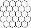
Fig. 4 shows low-density and conducts electricity micro-pattern, and this low-density pattern comprises the summit width to the limit of the hexagonal unit cells of wire that 3 μ m are wide and about 175 μ m, causes the activity coefficient of about 3% wire;
Fig. 5 shows the conductive pattern with the micro-area of the pattern of low-density, the micro-area of the pattern of this low-density is included in the wide wire of 3 μ m of the spacing of each the 200 μ m in two orthogonal directionss, cause the activity coefficient of about 3% wire, and comprise the larger feature of the continuous metal area format of 1.2mm * 1.2mm;
Fig. 6 shows the low-density embossing pattern of pressing mold, the rectilinear projection feature on the corresponding stamper surface of solid line, and dotted line has been drawn zone.The micro-pattern of this low-density comprises the wide linear protrusion feature of 3 μ m of the spacing of 700 μ m, causes the activity coefficient of about 1% protruding features;
Fig. 7 shows the low-density embossing pattern of pressing mold, the rectilinear projection feature on the corresponding stamper surface of solid line, and dotted line has been drawn zone.The micro-pattern of this low-density comprises the wide linear protrusion feature of 3 μ m of the spacing of 700 μ m, and has the breakpoint of about 10 μ m as shown in the figure, causes the activity coefficient of about 1% protruding features;
Fig. 8 is scanning electron micrograph, show the conductive pattern that comprises the micro-area of the pattern of low-density, the micro-area of the pattern of this low-density has the wide conducting metal wire of 3 μ m of square mesh form of the spacing of about 200 μ m, cause 3% activity coefficient, and there is the continuous metal zone of 2mm * 2mm;
Fig. 9 is scanning electron micrograph, shows the conductive pattern that comprises the micro-area of the pattern of low-density, and the micro-area of the pattern of this low-density has the wide conducting metal wire of 5 μ m of the square mesh form of 5% activity coefficient;
Figure 10 is scanning electron micrograph, show the conductive pattern that comprises the micro-area of the pattern of low-density, the summit that the micro-area of the pattern of this low-density has about 175 μ m is the wide conducting metal wire of 3 μ m of the sexangle mesh form of width to the limit, causes 3% activity coefficient;
Figure 11 is scanning electron micrograph, show the sub-fraction of the conductive pattern that comprises the micro-area of the pattern of low-density, the summit that the micro-area of the pattern of this low-density has 5% activity coefficient, about 175 μ m is the wide conducting metal wire of about 5 μ m of the sexangle mesh form of width (having drawn the fine rule that crosses three conduction line segments in image, for showing the width of line segment) to the limit;
Figure 12 is scanning electron micrograph, show the sub-fraction of the conductive pattern that comprises the micro-area of the pattern of low-density, the summit that the micro-area of the pattern of this low-density has 3% activity coefficient, about 175 μ m is the wide conducting metal wire of 3 μ m of the hexagonal graticule mesh well format of width (having drawn the fine rule that crosses three conduction line segments in image, for showing the width of line segment) to the limit;
Figure 13 shows the schematic diagram of touch panel sensor;
Figure 14 shows in the touchscreen senses zone skeleton view to the conductive region of visible transparent;
Figure 15, Figure 15 a and Figure 15 b show the different piece of the first patterned substrate;
Figure 16, Figure 16 a and Figure 16 b show the different piece of the second patterned substrate;
Figure 17 shows the transparent projected capacitive touch screen sensor element by the first patterned substrate of Figure 15 and Figure 16 and the second patterned substrate structure.
Accompanying drawing may not be drawn in proportion.The same numeral used in the accompanying drawings means identical parts.Yet, should be appreciated that and in given accompanying drawing, use the label indicating device to be not intended to limit the parts of using the same numeral mark in another accompanying drawing.
Embodiment
In the following description, with reference to the one group of accompanying drawing that forms this explanation part, and wherein by illustrating some specific embodiments.Should be appreciated that imagination and do not depart from the scope of the present invention or mental condition under can implement other embodiment.Therefore, following embodiment is not intended to be limited.
Except as otherwise noted, otherwise all Science and Technology terms that use in the present invention have the general implication in this area.Definition provided herein is intended being conducive to understand some term that this paper commonly uses, and does not mean that the scope of the present invention that limits.
Except as otherwise noted, otherwise in all cases, all numerals that are used for explaining characteristic dimension, quantity and physical characteristics in instructions and claims all are interpreted as being modified by term " about ".Therefore, unless the contrary indication, otherwise the numerical parameter of listing in above-mentioned instructions and claims is approximate value, and utilize instruction content disclosed herein to seek the desirable characteristics obtained according to those skilled in the art, these approximate values can be different.
By the numerical range of end points statement comprise in this scope all numerical value of comprising (as, 1 to 5 comprises 1,1.5,2,2.75,3,3.80,4 and 5) and any scope in this scope.
Unless context explicitly points out in addition, otherwise in this instructions and claims, singulative " " used and " described " have been contained and have had a plurality of embodiment that refer to thing.As used in this instructions and claims, the term "or" normally with it comprise " and/or " implication use, unless other implications indicated clearly in context.
Transmissivity as used herein, that " visible transparent " refers to the transmission level of at least one polarization state of visible ray is at least 80%, wherein percent transmission is normalized to the intensity of incident light (being optionally polarized light).Within " visible transparent " intended scope, be, the goods of transmission at least 60% incident light comprise that part stops that light is to the microscopic feature (as point, square or lines) of transmissivity lower than 60% (as 0%), and this feature structure for example has, between between 0.5 to 10 μ m or the smallest dimension between 1 to 5 μ m (width); Yet, in this case, for comprise microscopic feature and width be 1000 times of microscopic feature smallest dimension roughly each to etc. large zone, average transmittance still is greater than 60%.
Polymkeric substance " film " substrate is the polymeric material that pliability and intensity are enough to carry out the plain film form of volume to volume formal layout.So-called volume to volume, refer to and be wound up on supporting mass by material or unwinding from supporting mass, and the process be further processed by some way.The example of further processing comprises coating, cuts, blanking and be exposed to radiation etc.Polymer film can be made to multi-thickness, usually in the scope of about 5 μ m to 1000 μ m.In a plurality of embodiment, the thickness of polymer film about 25 μ m to about 500 μ m or approximately 50 μ m to about 250 μ m or approximately 75 μ m to the scope of about 200 μ m.For the film that has embossment structure on or whole two first type surfaces, the thickness of film refers to the average thickness of the area that crosses film.
" self assembled monolayer " typically refer to and adhere to (as, pass through chemical bond) from the teeth outwards and with respect to this surface and one deck molecule of even relative to each other adopting preferred orientation.Show, self assembled monolayer so fully covering surfaces consequently changes this surperficial characteristic.For example, the application self assembled monolayer can cause surface to reduce, and allows optionally etching not scribble the metal of self assembled monolayer.
The present invention relates to based on micro-contact printing and etched metal pattern method.As used herein, " metal " and " metallization " refers to the conductive material that is applicable to conduction for the expection purpose, such as first disposition metal or alloy.Improvement comprises preferred pattern geometries, and the combination of they and preferred inking parameter and printing parameter.Pattern geometries, inking parameter and printing parameter combination limit preferred metal pattern action pane, especially on polymer film.But the advantage of the first action pane be the Application standard die material and be easy to realize with the pressing mold embossment of controlling effectively and can repeatedly generate the metal pattern that comprises tiny wire and there is very little activity coefficient.But the advantage of the second action pane be the Application standard die material and be easy to realize with the pressing mold embossment of controlling effectively and can repeatedly generate the metal pattern with first area and second area, wherein first area comprises tiny wire and has very little activity coefficient, and second area is larger feature (being greater than tiny wire).Window also comprises using in cost-effective manner the preferred printing time of equipment, but comprises in addition the feasibility of enforcement.Although the present invention so is not restricted, example provided below will obtain the understanding to each aspect of the present invention through discussion.
Owing to there being a plurality of complicated factors, therefore use micro-contact printing and etching effectively, efficient and repeatedly the ability of patterning conductive material depend on the pattern geometries of protruding features.Complicated factor comprises the effect of the pattern of pressing mold protruding features to following aspect: i) the suprabasil local pressure in pressing mold or base plate contact area that is applied to as limited by protruding features; Ii) pressing mold between protruding features in the embossing pattern zone subsides; Iii) flexing of protruding features; And iv) form the effective dose of molecule in pressing mold or baseboard material near the SAM of different protruding features.
These effects affect the quality of micro-contact printing pattern in the following areas: i) advantageously avoid pin hole occurring in the expection conductive region after patterning; Ii) advantageously avoid the conductive region distortion that causes because of pressing mold or base plate feature flexing, and iii) advantageously avoid pressing mold in the zone between between the expection conductive region or base plate to subside and the external conductor deposition that causes.Control embossing pattern geometric configuration is complicated to basic phenomenon and the mechanism of these effects of the ability of effective patterning conductive material, and inconsistent each other in some cases.
Apply larger power and can in the contact area of between, produce larger local pressure between pressing mold or base plate and substrate; it has been found that; this contributes to shift to form usually makes conductive region carry out the molecular monolayer of the self assembled monolayer of etched pattern; and conductive region does not have the high density pin hole, but can cause in the zone between the embossing pattern protruding features occurring that pressing mold subsides.And for example; the spacing of also finding protruding features approaches together and helps avoid pressing mold and subside; and contribute to forming unexpected conductive region between the embossing pattern protruding features; but when feature more approaches together; pattern density can form molecule and produces obvious negative interaction obtain enough SAM from pressing mold or base plate, thereby causes the SAM mask of printing can't obtain the conductive region that there is no pin hole after etching.SAM with enough concentration is formed to molecule also to be applicable to protect the needs of the larger feature of the SAM with printing in etching process with the focus attentions equally on of protecting feature in high density patterns.And, importantly, if do not have the SAM of enough concentration to form molecule in pressing mold, and there is no can allow to form enough impressions time of enough SAM formations in large characteristic area, this type of parameter can have side effects to the characteristic dimension degree of accuracy of less feature so.Certainly, there is complicated interaction between a plurality of factors in the micro-contact printing patterning of conductor.Importantly, when attempt the application said method with the commericially feasible sexual needs carry out micro-contact printing and etching more and more at a high speed the time, the effect of above listing and describing in detail can become and in fact more be difficult to control.Although have this complicacy, have been found that some required conductive pattern geometric configuration derived from pressing mold or printed panel embossing pattern geometric configuration can and be etched with fair speed by micro-contact printing and be processed.
We find, by pressing mold, for printing during the etching mask based on SAM, some two-dimensional pattern geometric configuration of micro-contact printing pressing mold protruding features allows effectively, efficient and can repeatedly form the etching metal pattern.Pattern geometries in the present invention can adopt the multi-form of unlimited amount in fact, but they all meet some description, as described below.
All patterns all comprise density regions.So-called low-density, refer to the area fraction of pressing mold protruding features or the area fraction of the metal that carries out retaining after the pattern-like etching in substrate less, as described below.Term low density refers to pattern density, and this paper can exchange with activity coefficient.Low-density (low-density) and low density (low-density) are used interchangeably.Density regions area in pattern is 5mm at least
2, be preferably at least 10mm
2.In certain embodiments, the area of density regions is for being greater than 1 square centimeter of (cm
2), be greater than 10cm
2, be greater than 50cm
2, or even be greater than 100cm
2.
Whether in certain embodiments, pattern comprises density regions, to existing the zone of any other type not do requirement.In other embodiments, the zone that pattern comprises density regions and has larger pattern characteristics (for example, as wide wire or contact block, at least 10 μ m, preferably at least 25 μ m, the width of 100 μ m to 1000 μ m).As another example of the latter, the protruding features pattern on pressing mold (it limits the metal pattern after etching) can comprise size and identical larger protruding features as whole density regions was allowed, for example 5mm
2or larger.This type of protruding features should limit the zone itself that density or fill area are 1, and such zone is not density regions.The pressing mold pattern and therefore the metal after the pattern-like etching by the protruding features that limits two-dimentional embossing pattern, formed.In embossing pattern not in protruding features have this paper to be described as " the non-raised points " in embossing pattern.
Geometric configuration in density regions preferably includes the protruding features of non-parallel linear element form.What is called comprises non-parallel linear element, refers to that pattern comprises linear element, but is not that all linear elements are all parallel to each other.It has been found that, the geometric configuration that comprises non-parallel linear element has enlarged markedly the easy degree that can form the metal pattern with surprising low activity coefficient, for example is less than 10% or be less than 5% or be less than 4% or be less than 3% or be less than 2% or be less than 1% or the activity coefficient of even lower (for example 0.5%).Although these activity coefficient values of pattern or area of the pattern are preferred, are greater than 5%, are greater than 10% or even be greater than 15% pattern fills coefficient also in disclosure scope.In certain embodiments, the activity coefficient in density regions is between between 0.5 to 20%, in certain embodiments between between 0.5 to 15%, in certain embodiments between between 0.5 to 10%, in certain embodiments between between 0.5 to 5%, in certain embodiments between between 0.5 to 4%, in certain embodiments between 1 to 3%.
After the protruding features pattern of the pressing mold in density regions and etching, the pattern of conductor element also can be described with the distance value between adjacent feature and adjacent elements.Preferably, the distance between all adjacent protrusion features of the pressing mold in density regions is for being less than or equal to about 1mm.More preferably, in certain embodiments, the distance value between all adjacent protrusion features is for being less than or equal to about 500 μ m.Yet, between the distance value between adjacent feature and adjacent element, be greater than 1mm (for example, between between 1mm to 2mm or between between 1mm to 5mm) also in disclosure scope.Determine the distance value between the adjacent protrusion feature in density regions, at first will identify adjacent protruding features.For the density regions of the linear protrusion feature that comprises the two-dimensional mesh form, with for the density regions that comprises the protruding features separated, the identification of adjacent protrusion feature is different.At first consider the situation of the protruding features (for example limiting the protruding features of square mesh, hexagon mesh or other polygon mesh) of two-dimensional mesh form, the mesh unit that can limit in conjunction with them limits adjacent protruding features.For different mesh cell configurations, need to identify adjacent protruding features by different rules.At first, for the mesh unit (being that unit has the inner centre of form) that is positioned at open area for the centre of form of unit open area, the adjacent protrusion of this unit is characterized as and can draws and extend to through the centre of form may the short lines crossing protruding features on Liang Ge border, unit; And, the length that the distance value between the adjacent protrusion feature of this unit is this straight line.In the situation that just now described, except those protruding features that contacted by this straight line, other protruding features are considered as non-conterminous.Secondly, for the centre of form of unit open area is positioned at the outer mesh unit (being that unit has the outside centre of form) of open area, determine the adjacent protrusion feature of this unit, at first unit area to be divided into to the subelement zone of minimum number, require each subelement zone to there is oneself the centre of form (being that each subelement zone has the inner centre of form) in this subelement zone.Then, this type of mesh unit has just had multipair adjacent protruding features, every a pair of corresponding with each subelement zone.For each subelement zone, the adjacent protrusion in this subelement zone is characterized as and can draws and extend to through the centre of form in this subelement zone may the short lines crossing protruding features on these two borders, subelement zone; And, the length that the distance value between the adjacent protrusion feature in this subelement zone is this straight line.For the density regions of the separative protruding features of tool, those of ordinary skill in the art can more directly understand adjacent protruding features.They are the multipair protruding features that there is no other protruding features in gap therebetween.It has been found that, preferred density regions pressing mold embossing pattern geometric configuration comprises the protruding features that limits two-dimensional mesh, wherein the unit of mesh has the inner centre of form, and the distance value between the adjacent protrusion feature of unit is for being less than or equal to about 1mm or being less than or equal to about 500 μ m.
Preferably the activity coefficient of embossing pattern is consistent in density regions.More particularly, in density regions, preferably the variation of protruding features density (shared area fraction means with the protruding features in regional any part) is not more than particular differences coefficient (recently meaning with the percentage of the average density in whole density regions).The relative dimensions of this area portions comprises 1mm
2, 2mm
2, 5mm
2, and 10mm
2.In a plurality of embodiment, coefficient of variation is for being less than 75% or be less than 50% or be less than 25% or be less than 10% or be less than 5% or even less.
Fig. 1 to Fig. 5 provides the non-limiting setting of the available micro-pattern of conduction.Fig. 1 shows low-density and conducts electricity micro-pattern, and this low-density pattern is included in the wide wire of 3 μ m of the spacing of each the 200 μ m in two orthogonal directionss, causes the activity coefficient of about 3% wire.Fig. 2 shows low-density and conducts electricity micro-pattern, and this low-density pattern is included in the wide wire of 3 μ m of the spacing of each the 200 μ m in two orthogonal directionss, and has the breakpoint of about 10 μ m as shown in the figure, causes the activity coefficient of about 3% wire.Fig. 3 shows low-density and conducts electricity micro-pattern, and the about low-density pattern of 1.2mm * 1.2mm, and comprise the conductor segment of 40 separation that about 225 μ m are long, about 3 μ m are wide causes the activity coefficient of about 2% wire.Fig. 4 shows low-density and conducts electricity micro-pattern, and this low-density pattern comprises the summit width to the limit of the hexagonal unit cells of wire that 3 μ m are wide and about 175 μ m, causes the activity coefficient of about 3% wire.Fig. 5 shows the conductive pattern with the micro-area of the pattern of low-density, the micro-area of the pattern of this low-density is included in the wide wire of 3 μ m of the spacing of each the 200 μ m in two orthogonal directionss, cause the activity coefficient of about 3% wire, and comprise the larger feature of the continuous metal area format of 1.2mm * 1.2mm.
With regard to non-parallel linear element, it has been found that, preferred low-density pattern geometries is characterised in that to have a plurality of linear elements, and not around non-raised points all directions (in positive and negative 10 degree) upper with linear element apart from the non-raised points over a certain distance (being called " maximum spacing " with linear element herein).And the restriction of positive and negative 10 degree of assigned direction is confirmed between having minute opening between linear element also in disclosure scope.Linear element with minute opening is particularly suited for the pressing mold of supporting in the part in the zone of (for example, between mesh) between adjacent element in density regions.
Fig. 6 shows the low-density embossing pattern zone 100 of pressing mold, the linear protrusion feature on the corresponding stamper surface of solid line 110, and dotted line has been drawn zone.The micro-pattern of this low-density comprises the wide linear protrusion feature 110 of 3 μ m of the spacing of 700 μ m, causes the activity coefficient of about 1% protruding features.Non-raised points 120 is in the gap between protruding features.The vector 130 that magnitude is 1mm (together with attached vector 140 and 150) and the swingable all angles in the zone 160 of defining with dotted line (360 degree), and observe with an angled protruding linear element overlapping.In this case, it is said that non-raised points and linear protrusion characteristic are less than 1mm at directive maximum spacing.
Fig. 7 shows the low-density embossing pattern zone 200 of pressing mold, the linear protrusion feature on the corresponding stamper surface of solid line 210, and dotted line has been drawn zone.The micro-pattern of this low-density comprises the wide rectilinear projection feature 210 of 3 μ m of the spacing of 700 μ m, and has the breakpoint of about 10 μ m as shown in the figure, causes the activity coefficient of about 1% protruding features.Non-raised points 220 is in the gap between protruding features.The vector 230 that magnitude is 1mm (together with attached vector 240 and 250) and the swingable all angles in the zone 260 of defining with dotted line (360 degree), and observe with an angled protruding linear element overlapping.In this case, it is said that non-raised points and linear protrusion characteristic are less than 1mm at directive maximum spacing.
Preferably, as described above, the maximum spacing of all non-raised points and linear element is for being less than 1mm or being less than 750 μ m or being less than 500 μ m or being less than 400 μ m or being less than 300 μ m or being less than 100 μ m or being less than 50 μ m or even less.At least 3 times or more than 5 times or be greater than 10 times greatly of the major axis of linear element or its width of arc Length Ratio.In the zone that does not need electric continuity at the conductor element by derived from the pressing mold protruding features, those of ordinary skill in the art will understand that, it has been found that, by arrangement pitch, very near more elements such as axle such as grade can meet concrete layout and the shape needs of linear element, thereby form the in fact linear array of the element of tight spacing, this is favourable to printing.Under latter event, the linear array of the element of tight spacing is regarded as linear conductor unit.Linear element can be spaced, but in certain embodiments, preferably they are joined together to form net or mesh, for example square mesh or hexagon mesh or other polygon mesh.In a plurality of embodiment, the width of linear element is less than or equal to about 25 μ m or is less than or equal to about 10 μ m or is less than or equal to about 5 μ m or is less than or equal to about 2 μ m.In certain embodiments, the width of linear element is between between 0.5 to 25 μ m, in certain embodiments between between 0.5 to 10 μ m, in certain embodiments between between 1 to 10 μ m, in certain embodiments between between 1 to 5 μ m, in certain embodiments between between 1 to 4 μ m, in certain embodiments between between 1 to 3 μ m, in certain embodiments between 2 to 3 μ m.
For some application of the low activity coefficient metal pattern of needs, especially on polymer film substrate, it has been found that, it is 0.5% to 5% that the pressing mold pattern that has width and be the linear protrusion element two-dimensional mesh of 1 μ m to 10 μ m and be not greater than the non-raised points of 1mm with the maximum spacing of linear element is conducive to form activity coefficient, for example 2% or 3% metal pattern.Also find, it is 0.5% to 5% that the pressing mold embossing pattern that has width and be the linear protrusion element two-dimensional mesh of 2 μ m to 5 μ m and be not greater than the non-raised points of 750 μ m with the maximum spacing of linear element is conducive to form activity coefficient, for example 2% or 3% metal pattern.Also find, it is 0.5% to 5% that the pressing mold embossing pattern that has width and be the linear protrusion element two-dimensional mesh of 1 μ m to 3 μ m and be not greater than the non-raised points of 500 μ m with the maximum spacing of linear element is conducive to form activity coefficient, for example 2% or 3% metal pattern.
Above-mentioned die geometries (for example is conducive to solve the standard die material, the dimethyl silicone polymer (PDMS) of modulus between 0.5MPa to 5MPa, as Dow Corning (Midland, Michigan) problem of subsiding of the pressing mold PDMS sold with trade name Sylgard 184), pressing mold embossment size for following situation is especially true: i) the convenient generation, ii) there do not is the problem of protruding features flexing, and iii) can not cause ink molecules to form the long the evolving path that arrives print surface in the pressing mold volume.
For above-mentioned two-dimensional pattern geometric configuration, convenient and available pressing mold pattern embossment size is between between 0.5 to 10 μ m or between between 0.75 to 5 μ m or between 1 to 2 μ m especially.With other materials that can avoid pressing mold to subside (such as high-modulus PDMS), compare, preferably use above-mentioned standard die material, for example, because standard material provides the relative merit that relates to following content: the processing power that the transmission character favourable with it is relevant and the conformal ability contacted with non-smooth surface, the metalized surface of substrate (such as polymer film) (comparing with very level and smooth semiconductor wafer).
In certain embodiments, except density regions mentioned above, the conductive pattern so completed in the two-dimensional pattern of pressing mold and substrate also comprises larger feature.The minimum dimension of larger feature is at least 25 μ m.The example of larger feature comprises the line of at least 25 μ m width (minimum dimension) and the square block of at least 25 μ m length of sides (minimum dimension).In the situation that complex geometric shapes, for example, in the situation that the conductor deposit of adjacency can comprise tiny element and larger element, those of ordinary skill in the art will know, tiny element is connected with larger element and can not makes to be down to as the minimum dimension of the larger element of feature itself size of tiny element.Can more clearly understand by way of example, suprabasil contiguous conductor sediment comprises the square block of 1mm * 1mm, also comprise the tiny wire (as wide as 1 μ m) be connected on this piece, for example can form the low-density mesh, this conductor deposit forms (the be connected minimum dimension of the feature that can not make to comprise piece of the wide wire piece wide with 1mm * 1mm of 1 μ m is 1 μ m, so is not regarded as larger feature) by larger feature (piece) and low-density mesh.In certain embodiments, the minimum dimension of larger feature at least 50 μ m, in certain embodiments at least 100 μ m, in certain embodiments at least 200 μ m, in certain embodiments at least 500 μ m, be 1mm at least in certain embodiments.
For by micro-contact printing, then etching and form in cost-effective manner above-mentioned metal pattern geometric configuration, preferred pressing mold inking operation and inking parameter and printing parameter have been had been found that.More particularly, for the actual high speed printing of the etching mask based on SAM, preferred molecule and the concentration in pressing mold thereof are disclosed.This molecule forms the mercaptide individual layer on metal surface, and comprises sulfane, dialkyl disulphides, dialkyl sulfide, alkyl xanthate, dithiophosphates and dialkylthiocarbamate.This molecule is characterised in that the tail base be attached on sulphur atom, and wherein this tail base has 14 to 20 atoms along its main chain, is preferably 16,17 or 18 atoms.Atom along main chain is preferably carbon atom.Preferably ink solutions comprises alkyl sulfhydryl, is for example straight chained alkyl mercaptan:
HS(CH
2)
nX
Wherein n is the MU (methylene unit) number, the end group that X is alkyl chain (for example, X=-CH
3,-OH ,-COOH ,-NH
2deng).Preferably, X=-CH
3, n=15,16 or 17, corresponding 16,17 or 18 chain length respectively.Other available chain lengths comprise 19 and 20.For having for for the linear molecule of the sulfur-bearing head group of connection metal, chain length is defined as the linearly aligned atomicity along bonded atom, and chain length is in the atom on being bonded to sulphur atom and linear array between last carbon atom and comprise them.The unimolecular layer formation molecule of meeting branching also, in disclosure scope, for example has the side group on the linear array that is attached to the bonded atom that limits chain.Available end group comprises those of the following stated for example: (1) Ulman, " Formation and Structure of Self-Assembled Monolayers; " Chemical Reviews Vol.96, pp.1533-1554 (1996) (Ulman, " formation of self assembled monolayer and structure ", " chemistry comment ", the 96th volume, 1533-1554 page (1996)); (2) Love et al., " Self-Assembled Monolayers of Thiolates on Metals as a Form of Nanotechnology; " Chemical Reviews Vol.105, pp.1103-1169 (the 2005) (people such as Love, " as the self assembled monolayer of the mercaptide on the metal of nanometer technology form ", " chemistry comment ", the 105th volume, 1103-1169 page (2005)).It can be partially fluorinated or fluoridized that SAM forms molecule.Every this paper forms molecule by some SAM and is called availablely or preferred, it should be appreciated by those skilled in the art, other molecules of sharing the important printing attribute of desired use with those molecules are also same available or preferred.
SAM forms molecule and is present in pressing mold, and contiguous print surface, preferably in the prescribed concentration scope.With respect to the print surface adjacency with pressing mold, adoptable concentration is specified for being defined as the pressing mold volume of distance in 10 μ m with stamping surface.Can use following methods to measure the concentration in pressing mold: for example, by the microsection technology, from the print surface of pressing mold, to cut thin layer of elastomer, then this thin layer is carried out to chemical analysis, for example can or can at first from thin layer, not leach individual layer and form molecule.Available analytical approach comprises mass spectroscopy and spectroscopic method, all NMR (Nuclear Magnetic Resonance) spectrum as known in the art or infrared spectrum.
With reference to the above-mentioned pattern geometries explanation to pattern with density regions, found with micro-contact printing and etching can be effective, efficient and the renewable place of production realize that the plated metal conductor forms pattern in substrate, wherein in contiguous above-mentioned print surface place pressing mold, the concentration of 16 carbon mercaptan (HDT) is between 0.05 to 5 mM, in conjunction with the impression time be between 0.1 to 10 second.Use the preferred distance in the concentration between 0.1 to 1 mM and time qualified this window of the impression between 0.5 to 5 second.Use the more preferably spacing in the concentration between 0.1 to 0.5 mM and time qualified this window of the impression between 0.5 to 5 second.Outside these windows, it is found that the conductive pattern after etching is defective, defect is that etching selectivity is poor or cause the disabled feature of final pattern to broaden.About validity, high efficiency and the repeatability of patterning, above-mentioned processing window makes the impression time enough short in to reduce costs, but can too short so that more difficult control.Window also can limit the technique spacing, it is found that the global pattern quality of enough consistent characteristic dimension and quick continuous printing is repeatably.Outside this window, other combinations of technological parameter are not enough to allow to repeat maximum 10 printings according to proof.By contrast, the parameter in above-mentioned window allows to be greater than the quick continuous printing of 10 times, and has outstanding pattern quality and available characteristic dimension degree of accuracy.Impress the time by combining target, found that above-mentioned concentration range can be used for having the pattern of density regions, for example has the density regions of above-mentioned tiny characteristics.Preferably, after being applied in substrate by pressing mold, with respect to the actual contact area between pressing mold and substrate, during printing, applied pressure is between 0 kPa to 10 kPas.It is above-mentioned that to be regarded as can be used for length for 16 carbon mercaptan and for example, process window with pattern of density regions (tiny characteristics) be that 16 atoms (do not comprise head group, mercaptan head group for example, and be not hydrogen atom) or with other unimolecular layers that 16 carbon mercaptan are shared important printing attribute form molecules.
With reference to the above-mentioned pattern geometries explanation to pattern with density regions, found with micro-contact printing and etching can be effective, efficient and the renewable place of production realize that the plated metal conductor forms pattern in substrate, wherein in contiguous above-mentioned print surface place pressing mold, the concentration of 18 carbon mercaptan (HDT) is between 0.5 to 20 mM, in conjunction with the impression time be between 0.1 to 10 second.Use the preferred distance in the concentration between 0.5 to 10 mM and time qualified this window of the impression between 0.5 to 5 second.Use the more preferably spacing in the concentration between 0.5 to 5 mM and time qualified this window of the impression between 0.5 to 5 second.Outside these windows, it is found that the conductive pattern after etching is defective, defect is that etching selectivity is poor or cause the disabled feature of final pattern to broaden.About validity, high efficiency and the repeatability of patterning, above-mentioned processing window makes the impression time enough short in to reduce costs, but can too short so that more difficult control.Window also can limit the technique spacing, it is found that the global pattern quality of enough consistent characteristic dimension and quick continuous printing is repeatably.Outside this window, other combinations of technological parameter are not enough to allow to repeat maximum 10 printings according to proof.By contrast, the parameter in above-mentioned window allows to be greater than the quick continuous printing of 10 times, and has outstanding pattern quality and available characteristic dimension degree of accuracy.Impress the time by combining target, found that above-mentioned concentration range can be used for having the pattern of density regions, for example has the density regions of above-mentioned tiny characteristics.Preferably, after being applied in substrate by pressing mold, with respect to the actual contact area between pressing mold and substrate, during printing, applied pressure is between 0 kPa to 10 kPas.It is above-mentioned that to be regarded as can be used for length for 18 carbon mercaptan and for example, process window with pattern of density regions (tiny characteristics) be that 18 atoms (do not comprise head group, mercaptan head group for example, and be not hydrogen atom) or with other unimolecular layers that octadecyl mercaptan is shared important printing attribute form molecules.18 carbon mercaptan and similar molecular proportion 16 carbon mercaptan and similar molecule are preferred.
With reference to the above-mentioned pattern geometries explanation to pattern with density regions and larger feature, found with micro-contact printing and etching can be effective, efficient and the renewable place of production realize that the plated metal conductor forms pattern in substrate, wherein in contiguous above-mentioned print surface place pressing mold, the concentration of 16 carbon mercaptan is between 0.5 to 5 mM, in conjunction with the impression time be between 0.1 to 10 second.Use the preferred distance in the concentration between 0.5 to 1 mM and time qualified this window of the impression between 0.5 to 5 second.Outside these windows, it is found that the conductive pattern after etching is defective, defect is that etching selectivity is poor or cause the disabled feature of final pattern to broaden.About validity, high efficiency and the repeatability of patterning, above-mentioned processing window makes the impression time enough short in to reduce costs, but can too short so that more difficult control.Window also can limit the technique spacing, it is found that the global pattern quality of enough consistent characteristic dimension and quick continuous printing is repeatably.Outside this window, other combinations of technological parameter are not enough to allow to repeat maximum 10 printings according to proof.By contrast, the parameter in above-mentioned window allows to be greater than the quick continuous printing of 10 times, and has outstanding pattern quality and available characteristic dimension degree of accuracy.Impress the time by combining target, found that above-mentioned concentration range can be used for having the pattern of density regions, for example has the density regions of above-mentioned tiny characteristics.Preferably, after being applied in substrate by pressing mold, with respect to the actual contact area between pressing mold and substrate, during printing, applied pressure is between 0 kPa to 10 kPas.It is above-mentioned that to be regarded as can be used for length for 16 carbon mercaptan and for example, process window with pattern of density regions (tiny characteristics) be that 16 atoms (do not comprise head group, mercaptan head group for example, and be not hydrogen atom) or with other unimolecular layers that 16 carbon mercaptan are shared important printing attribute form molecules.
With reference to the above-mentioned pattern geometries explanation to pattern with density regions and larger feature, found with micro-contact printing and etching can be effective, efficient and the renewable place of production realize that the plated metal conductor forms pattern in substrate, wherein in contiguous above-mentioned print surface place pressing mold, the concentration of 18 carbon mercaptan is between 0.5 to 20 mM, in conjunction with the impression time be between 0.1 to 10 second.Use the preferred distance in the concentration between 0.5 to 10 mM and time qualified this window of the impression between 0.5 to 5 second.Use the more preferably spacing in the concentration between 1 to 5 mM and time qualified this window of the impression between 0.5 to 5 second.Outside these windows, it is found that the conductive pattern after etching is defective, defect is that etching selectivity is poor or cause the disabled feature of final pattern to broaden.About validity, high efficiency and the repeatability of patterning, above-mentioned processing window makes the impression time enough short in to reduce costs, but can too short so that more difficult control.Window also can limit the technique spacing, it is found that the global pattern quality of enough consistent characteristic dimension and quick continuous printing is repeatably.Outside this window, other combinations of technological parameter are not enough to allow to repeat maximum 10 printings according to proof.By contrast, the parameter in above-mentioned window allows to be greater than the quick continuous printing of 10 times, and has outstanding pattern quality and available characteristic dimension degree of accuracy.Impress the time by combining target, found that above-mentioned concentration range can be used for having the pattern of density regions, for example has the density regions of above-mentioned tiny characteristics.Preferably, after being applied in substrate by pressing mold, with respect to the actual contact area between pressing mold and substrate, during printing, applied pressure is between 0 kPa to 10 kPas.It is above-mentioned that to be regarded as can be used for length for 18 carbon mercaptan and for example, process window with pattern of density regions (tiny characteristics) be that 18 atoms (do not comprise head group, mercaptan head group for example, and be not hydrogen atom) or with other unimolecular layers that 18 carbon mercaptan are shared important printing attribute form molecules.18 carbon mercaptan and similar molecular proportion 16 carbon mercaptan and similar molecule are preferred.
Also can determine concentration range according to the needs of avoiding on stamper surface or in pressing mold, the worthless SAM of formation forms the molecule precipitation to a certain extent, be the concentration range that above-mentioned SAM forms molecule specifically.It is found that, although some concentration is that high concentration (as be 18 carbon mercaptan of 10 mMs in PDMS) can be used for printing specifically, can and produce worthless precipitation reuse the time in expansion, and expansion and reuse emphasis of the present invention just.When using 20 mercaptan (20 carbochain mercaptan), this sedimentation problem is especially thorny, but can not develop into molecule, can not use.
SAM forms the above-mentioned specification of molecule and concentration, especially for preferred molecule, causes formation especially can generate with high-throughput the inking pressing mold of the mask based on SAM of above-mentioned geometric configuration, especially in the substrate of metallized polymeric film.It has been found that, preferred inking pressing mold can commericially feasible the print pass impression or print the SAM mask of above-mentioned geometric configuration, thereby solution can be used as enough SAM perfections of etching mask and the needs that limited SAM scatters best, be preferably used for some substrate, for example polymer film substrate.According to the present invention, be the duration of contact of pressing mold and metal surface (printing time) between 0.1 to 30 second, preferably between 0.1 to 10 second, more preferably between 0.5 to 5 second.
The above-mentioned impression carried out with above-mentioned pressing mold or typography can not cause any horizontal pressure force subsided to be carried out by applying between pressing mold and substrate.The example of available stress level comprises and is less than 100 kPas, is less than 50 kPas, is less than 25 kPas or even be less than 10 kPas.Method as herein described is particularly useful for forming metal pattern in the situation that do not apply large pressure by micro-contact printing.Apply the transfer mass that larger pressure can improve SAM, thereby form better etching mask, but can destroy because of the pressing mold distortion fidelity of pattern.
Above-mentioned inking pressing mold and printing condition are particularly useful for repeating to impress the etching mask patterns based on SAM of above-mentioned geometric configuration.What is called repeats impression, after referring to the pressing mold inking, can use pressing mold repeatedly on new zone, metal surface, to form the etching mask of printing, for example, on new base metallization.The pressing mold of inking can be used for being greater than 5 times or is greater than 10 times or is greater than 20 times or be greater than 30 times or be greater than 40 times or be greater than 50 printings, and without repeating the inking step.The time of this type of carrying out with the above-mentioned pressing mold with its embossing pattern and printing ink concentration between repeating print is preferably shorter, for example is less than 30 seconds or is less than 15 seconds or is less than 10 seconds or is less than 5 seconds.
For the pattern that comprises the tie point between density regions and larger feature, wherein the linear feature in density regions or element contact with larger feature, and some pattern geometries is included in and makes linear feature widen this linear feature before contacting with larger feature.For example, can make the wide linear element of 1 to 5 μ m contacted with larger feature be tapered from larger feature, until its length is its width 1 to 10 times.Taper contributes to the patterning of remaining valid.For some inking parameters and printing parameter, the SAM printed in etching process can not protect the part of this type of narrower linear element and contacting of larger feature fully, thereby causes near the linear element of larger feature deteriorated.
Available visible transparent substrate comprises polymer film.Available polymer film comprises thermoplasticity and thermosetting polymer film.The example of thermoplastics comprises polyolefin, polyacrylate, polyamide, poly-acid imide, polycarbonate and polyester.Other examples of thermoplastics comprise the polycarbonate of tygon, polypropylene, poly-(methyl methacrylate), bisphenol-A, poly-(vinyl chloride), poly-(terephthalic acids ethyl ester) and poly-(vinylidene fluoride).
The visible transparent substrate that scribbles metal comprises above-mentioned polymer film, has the inorganic material coating (as metallic coating) of supporting self assembled monolayer on this polymer film substrate, can be then by etching by this coating patterns.Inorganic material coating can comprise for example first disposition metal, metal alloy, intermetallic compound, metal oxide, metal sulfide, metal carbide, metal nitride and their combination.The potpourri, alloy and the compound that comprise gold, silver, palladium, platinum, rhodium, copper, nickel, iron, indium, tin, tantalum and these elements for the exemplary inorganic material surface that supports self assembled monolayer.Inorganic material coating on polymeric substrates can be any thickness, is for example 1 nanometer to 3000 nanometer (nm).Inorganic material coating can be taked any deposition of method easily, for example sputter, evaporation, chemical vapor deposition or chemical solution deposition (comprising electroless plating).
Above-mentioned favourable pattern geometries, inking condition and printing condition have been confirmed to be and have been equally applicable to subsequently by some metal of etched patternization.Preferred metal is silver, gold and palladium, but the metal of other applicable etched patterns also within the scope of the invention.SAM mask formed according to the present invention is particularly useful for thickness between between 5 to 1000nm or between between 10 to 500nm or between between 15 to 200nm or the etched pattern of the above-mentioned metal between 20 to 100nm.Can before patterning, with any known deposition process, metal be deposited in substrate, comprise and use vapor phase transport process, such as sputter or evaporation, or use solwution method, such as electroless plating.Can use methods known in the art to carry out etching.
In certain embodiments, the method that is used to form metal pattern comprises the embossment relation reversed between pressing mold or base plate and substrate, and this is contrary to the above.That is, in these embodiments, above-mentioned pressing mold embossing pattern is as the feature of substrate, and pressing mold is substantially without feature.Aspect every other, for example comprise that, aspect pattern geometries, metal, inking and printing time, these embodiment are same as the previously described embodiments, all use pressing mold or base plate and the flat substrate of embossment structure.The example of available metallization embossment structure substrate is micro-science polymer film that silver-colored steam applies.Available for example do not have pressing mold (as PDMS) or the roll printing plate of the mercaptan immersion of embossment structure that the self assembled monolayer mask is transferred to the elevated regions that substrate surface scribbles the embossing pattern of conductor.In follow-up step, from the etched conductors optionally of the complementary region with the embossing pattern protruding features, thereby form conductive pattern according to the protruding features pattern.
Figure 13 shows the schematic diagram of touch panel sensor 100.Touch panel sensor 100 comprises the touch panel 110 with touch sensitive areas 105.Touch sensitive areas 105 is electrically connected to touch sensor drive unit 120.Touch panel 110 is incorporated in display device.
Figure 14 shows the skeleton view to the conductive region 301 of visible transparent, and it is positioned at touch sensitive areas 305.Conductive region 301 to visible transparent comprises visible transparent substrate 330 and is arranged in visible transparent substrate 330 or the micro-pattern 340 of interior conduction.Visible transparent substrate 330 comprises first type surface 332, and it is electrical isolation.Visible transparent substrate 330 can for example, be formed by any available electrically insulating material (glass or polymkeric substance).The examples of polymer that can be used for visible transparent substrate 330 comprises polyethylene terephthalate (PET) and PEN (PEN).Can conduct electricity micro-pattern 340 by a plurality of linear metal Characteristics creations that form according to methods described herein.
Figure 14 also shows the coordinate system that is positioned at the conductive region to visible transparent 301 of touch sensitive areas 305 for description.In general, with regard to display device, x axle and y axle be corresponding to width and the length of display, and the z axle is usually along thickness (i.e. height) direction of display.Unless otherwise noted, otherwise this paper will be used this rule all the time.In the coordinate system of Figure 14, x axle and y axle are restricted to the first type surface 332 that is parallel to visible transparent substrate 330, and can be corresponding to Width and the length direction of square or square surface.The z axle is perpendicular to this first type surface, and usually along the thickness direction of visible transparent substrate 330.The width of a plurality of linear metal features of the micro-pattern 340 of formation conduction is corresponding to the x direction distance of the parallel linear metallicity of extending along the y axis linear, and the y direction distance of orthogonal linear metallicity is corresponding to the width of orthogonal linear metallicity.The thickness of linear metal feature or height are corresponding to z direction distance.
In certain embodiments, the conductive region to visible transparent 301 that is positioned at touch sensitive areas 305 comprises the two-layer or more multi-layered visible transparent substrate 330 with the micro-pattern 340 of conduction.
Micro-pattern 340 that conducts electricity is deposited on first type surface 332.Because sensor will be connected to form with display touch-screen display or touch panel display, 330 pairs of visible transparent of substrate, and basically smooth.It is smooth and flexible that substrate and sensor can be essentially.Visible transparent is meaned to can see through touch sensor checks the information (for example text, image or numeral) that display provides.For the touch sensor of the conductor that comprises plated metal (if metal is deposited as to suitable micro-pattern, even can comprise that deposit thickness is enough to stop the metal of light) form, can realize observability and the transparency.
Micro-pattern 340 that conducts electricity comprises at least one conductive region to visible transparent, and this zone covers the visible part of the display that information is provided.So-called " to the conduction of visible transparent " refers to that can see through the micro-area of the pattern of conduction sees this partial display device, and this micro-area of the pattern conducts electricity in the plane of pattern, or in other words, along the micro-pattern of conduction, deposit to it on or the first type surface of adjacent substrate with it conducts electricity.The micro-pattern of preferred conduction comprises the have two-dimensional mesh zone of (for example square node or regular hexagon network), and wherein wire defines the open area of mesh inner sealing, and this zone does not deposit the conductor that the wire with mesh electrically contacts.This paper by open space with and the associated conductor wire of edge be called unit.The available geometric configuration of other of mesh unit comprises random cells shape and irregular polygon.
In one exemplary embodiment, provide the method for preparing touch panel sensor, the method comprises provides the visible transparent substrate that scribbles metal that comprises the embossing pattern with protruding features, and wherein embossing pattern has at least 5mm of measurement
2density regions.The protruding features of density regions has between the average area density value between 0.5 to 10%, has between the straight-line segment of width value between 0.5 to 25 μ m and be less than the distance value between the adjacent protrusion feature of 1mm.The method comprises that the inking elastic body pressing mold contact that will form the molecule inking with self assembled monolayer is coated with the visible transparent substrate of metal, and then etching metal is to form the micro-pattern of conduction on the protruding features in the visible transparent substrate.
In another exemplary embodiment, the method of the conductor on the patterned substrate is provided, concentration in the pressing mold of the chain length that provides the pressing mold of the inking with the embossing pattern that comprises protruding features, this inking pressing mold to comprise linear organic sulfur-containing self assembled monolayer to form molecule, 16 to 18 atoms, 1 to 10 mM, at least 5mm of measurement are provided the method
2the embossing pattern of density regions.The protruding features of density regions has between the straight-line segment of the average area density value between 0.5 to 5%, about 1 to 4 μ m width value, is less than the distance value between the adjacent protrusion feature of 1mm, the protruding features of at least 25 μ m width.The method comprises the visible transparent substrate that makes the contact of inking pressing mold scribble metal, the duration of contact in 0.5 to 10 second scope of contact procedure, thereby the pattern of deposition self assembled monolayer.The method also comprises that etching metal to form the electrically conducting transparent micro-pattern corresponding with the protruding features of inking pressing mold in the visible transparent substrate.
In another exemplary embodiment, the method of the conductor on the patterned substrate is provided, concentration in the pressing mold of the chain length that provides the pressing mold of the inking with the embossing pattern that comprises protruding features, this inking pressing mold to comprise linear organic sulfur-containing self assembled monolayer to form molecule, 16 to 18 atoms, 1 to 10 mM, at least 5mm of measurement are provided the method
2the embossing pattern of density regions.The protruding features of density regions has between the straight-line segment of the average area density value between 0.5 to 5%, about 1 to 4 μ m width value, is less than the distance value between the adjacent straight line segment of 1mm, the protruding features of at least 150 μ m width.The method comprises the visible transparent substrate that makes the contact of inking pressing mold scribble metal, the duration of contact in 0.5 to 10 second scope of contact procedure, thereby the pattern of deposition self assembled monolayer.The method also comprises that etching metal to form the electrically conducting transparent micro-pattern corresponding with the protruding features of inking pressing mold in the visible transparent substrate.
In another exemplary embodiment, the method of the conductor on the patterned substrate is provided, the method comprises that the linear organic sulfur-containing self assembled monolayer that provides the pressing mold of the inking with the embossing pattern that comprises protruding features, this inking pressing mold to have to comprise 18 carbon mercaptan forms the concentration in the pressing mold of molecule, 1 to 10 mM, at least 5mm of measurement
2the embossing pattern of density regions.The protruding features of density regions has the width between the protruding features of the straight-line segment of the average area density value between 0.5 to 5%, about 1 to 4 μ m width value, the distance value between the adjacent straight line segment that is less than 1mm, at least 150 μ m.The method comprises the visible transparent substrate that makes the contact of inking pressing mold scribble metal, and the duration of contact of contact procedure is in the scope of 0.5 to 5 second, thus the pattern of deposition self assembled monolayer.The method also comprises that etching metal to form the electrically conducting transparent micro-pattern corresponding with the protruding features of inking pressing mold in the visible transparent substrate.
In another exemplary embodiment, the method of the conductor on the patterned substrate is provided, the method comprises that the linear organic sulfur-containing self assembled monolayer that provides the pressing mold of the inking with the embossing pattern that comprises protruding features, this inking pressing mold to have to comprise 18 carbon mercaptan forms the concentration in the pressing mold of molecule, 1 to 10 mM, at least 5mm of measurement
2the embossing pattern of density regions.The protruding features of density regions has between the straight-line segment of the average area density value between 0.5 to 5%, about 1 to 4 μ m width value, is less than the distance value between the adjacent straight line segment of 1mm, the protruding features of 0.25mm width at least.The method comprises the visible transparent substrate that makes the contact of inking pressing mold scribble metal, and the duration of contact of contact procedure is in the scope of 0.5 to 5 second, thus the pattern of deposition self assembled monolayer.The method also comprises that etching metal to form the electrically conducting transparent micro-pattern corresponding with the protruding features of inking pressing mold in the visible transparent substrate.
example
pressing mold is manufactured
By preparing photoresist (Shipley1818 on the silicon chip that is 10 centimetres (cm) at diameter, Rohm and Haas company (Philadelphia, Pennsylvania)) pattern forms two different master molds for the molded elastomeric pressing mold.Different master molds is based on two kinds of different design, and this paper is called design " V1 " and design " V2 ".This design has some common elements and some differences.The design total area is 5cm * 5cm, and comprises the wide framework of 1mm (open area in following mask and with the protruding features in dip mold).In addition, it is about 33mm, the width a series of low-density mesh bars in the scope of 0.8mm to 1.2mm that design includes 20 length, the contact block end-blocking of mesh strip adoption 2mm * 2mm.Except framework, mesh bar and contact block, these two kinds of designs also are included between between the mesh bar and the separation characteristic in the space between mesh bar and framework.The size and dimension of separation characteristic is different, and minimum dimension is in the scope of 3 μ m to 100 μ m.Design V1 has 5.95cm in mask
2the open area total area, this is also the elevated regions total area on the gained pressing mold.Design V2 has 4.37cm in mask
2the open area total area, this is also the elevated regions total area on the gained pressing mold.Prepare master mold, can, by the photoresist rotary casting to silicon chip, be poured into the thickness of about 1.8 μ m.For each master mold, use the independent binary chrome photomask exposure photoresist that there is opening in the chromium material, in order to carry out patterning, wherein the opening in the chromium material defines the low-density pattern of straight-line segment together with 2mm * 2mm square block.After development of photoresist, form the master mold that comprises the binary embossing pattern, pattern has the recessed feature of the density regions distribution form of straight-line segment and piece.For two master molds, the part with pattern that the density regions of straight-line segment distributes comprises different low density web hole geometry (for example square net), its have 3 μ m and 5 μ m wide for limiting the wire of mesh.The open zone thresholding in selected mesh zone is 90%, 93%, 95% and 97% (being that characteristic density is respectively 10%, 7%, 5% and 3%).The scanning electron micrograph of the part that Fig. 8 is institute's finishing patterns, show the two-dimensional mesh area arrangement of the piece with higher degree open area and 2mm * 2mm.The scanning electron micrograph that Fig. 9 and Figure 10 are institute's finishing patterns (the silver-colored film on PET), show the geometric configuration (be respectively the square shaped cells geometric configuration with 95% open area and the wide wire of 5 μ m, there is the hexagonal cells geometric configuration of 97% open area and the wide wire of 3 μ m) of two micro-area of the pattern of low-density two dimension.Topple over the uncured dimethyl silicone polymer that about 3.0mm is thick (PDMS, SylgardTM 184, Dow Corning (Midland, Michigan)) on master mold, near master mold molded elastomeric pressing mold.Be exposed to vacuum by the uncured silicones that will contact master mold and make it degassed, then solidify 2 hours under 70 ℃.After master mold is peeled off pressing mold, form the PDMS pressing mold with embossing pattern, there is the high protruding features of about 1.8 μ m in embossing pattern, and there is the density regions distribution of straight-line segment and piece.Pressing mold is cut into to the size of about 5 * 5cm.
inking
Allow the back side (first type surface that there is no embossing pattern) of pressing mold contact the time (inking time) of appointment with the ethanolic solution of alkyl sulfhydryl, make the pressing mold inking.The alkyl sulfhydryl molecule used is 16 carbon mercaptan (" HDT " H0068, TCI America (Wellesley Hills, Massachusetts)) and 18 carbon mercaptan (" ODT " O0005, TCI AMERICA).Concentration and inking time to alkyl sulfhydryl solution are selected, and make and can obtain the aimed concn of alkyl sulfhydryl in the PDMS pressing mold of contiguous print surface, use finite-difference modeling computer program and the coefficient of diffusion value recorded to determine this concentration.For HDT, for the coefficient of diffusion value of simulating, be 6.6E-7cm
2/ second, this is the HDT diffuseness values in the PDMS of known ethanol swelling.For ODT, use two different coefficient of diffusion values to be simulated, in order to obtain the expection concentrations of mercaptans scope in contiguous print surface place pressing mold.Two values of ODT are 4.0E-7cm
2/ second, this is the ODT diffuseness values in known PDMS, and 6.6E-7cm
2/ second, this is the HTD diffuseness values in the PDMS of known ethanol swelling.The ODT coefficient of diffusion value of using is regarded as minimum and the highest probable value, will in following instance, with them, describe 18 transmission of carbon mercaptan in PDMS.Therefore, by calculating the expection concentration range that can determine contiguous print surface place 18 carbon mercaptan in example.Therefore, in following instance, record each concentration value of 16 carbon mercaptan and record the concentration value scope of 18 carbon mercaptan.
impression
Impression metallized polymeric film substrate after the pressing mold inking.In each situation, the film substrate is polyethylene terephthalate (ST504, DuPont (Wilmington, Delaware)).At first by hot evaporation (DV-502A, Denton Vacuum (Moorestown, New Jersey)) metallizing film in substrate.For all examples, be all at first on substrate surface, to apply the chromium of 20 dusts, and then apply the silver-colored or golden of 100nm.After metallization, with above-mentioned inking pressing mold embossed film.The area of metalized film substrate is about 6 * 6cm.During impression, make metalized film contact the embossing pattern surface of heads pressing mold, at first make the edge contact stamper surface of membrane sample, the hand-held rubber rollers that is then about 3.5cm with diameter makes film contact with pressing mold by rolling film.The time that carrying out the rolling step needs is less than 1 second.In following instance, the impression time is given, the impression time with substrate is rolled on pressing mold after extra duration of contact between substrate and pressing mold consistent.After fixed time, from pressing mold, at the bottom of stripping group, the time that this step needs is less than 1 second.In some cases, as described below, apply extra weight on substrate-die module after being applied on pressing mold by substrate and during impression.The flat glass that extra weight is the heavy 120g of a slice adds the flat Ceramic Tiles that a tablet quality is 140g, and general assembly (TW) is 260g.For design V1, the contact area during its impression is 5.95cm
2, the 260g weight applied is equivalent to apply 4.3 kpa pressures between the protruding features between substrate and pressing mold.For design V2, the contact area during its impression is 4.37cm
2, be applied to 260g weight and be equivalent to apply 5.8 kpa pressures between the protruding features between substrate and pressing mold.
etching
After impression, the metalized film that will have printed patterns immerses in etchant solutions, in order to carry out selective etch and metal pattern.Metalized film substrate for the printing that scribbles gold thin film, etchant comprises 1g thiocarbamide (T8656, Sigma-Aldrich (St.Louis, Missouri)), 0.54ml concentrating hydrochloric acid (HX0603-75, EMD Chemicals, Gibbstown (New Jersey)), 0.5ml hydrogen peroxide (30%, 5240-05, Mallinckrodt Baker (Phillipsburg, New Jersey)) and the 21g deionized water.For the patterned gold film, the metalized film substrate of printing is immersed in etching solution and kept 50 seconds.Metalized film substrate for the printing that scribbles silver-colored film, etchant comprises 0.45g thiocarbamide (T8656, Sigma-Aldrich (St.Louis, Missouri)), the 1.64g ferric nitrate (216828, Sigma-Aldrich (St.Louis, Missouri)) and the 200ml deionized water.For patterning silver film, the metalized film substrate of printing is immersed in etching solution and kept 3 minutes.After pattern etched gold or silver, with 2.5g potassium permanganate (PX1551-1, EMD Chemicals), 4g potassium hydroxide (484016, Sigma-Aldrich) and the chromium of the solution remnant of 100ml deionized water.
characterize
After optionally carrying out etching and metal pattern, by optical microscope (BH-2 type, be equipped with the DP12 digital camera, Olympus America (Center Valley, Pennsylvania)), scanning electron microscope (SEM, JSM-6400 type, JEOL Ltd (Tokyo, Japan)) and ohmer (GoldStar DM-313, LG Precision Co.Ltd. (Korea)) carry out the characterizing metal pattern.Determine the fidelity of the expection pattern of the film metal formed by etching by microscopic techniques.Measure the width of the linear feature of metal pattern, and compare with the Nominal Width value of 3 μ m and 5 μ m.According to the print characteristics size whether surpass respectively nominal size 0 μ m, approximately>0 to≤0.5 μ m, approximately>0.5 to≤1.0 μ m, approximately>1.0 to≤1.5 μ m or>1.5 μ m, assignment sizes degree of accuracy quality factor 5,4,3,2 or 1.Also by microscopic techniques, judge the etching selectivity in bulk zone (2mm * 2mm).Distribute large feature selecting quality factor 1,2,3,4 or 5, (5 is E.B.B., in etching process, substantially there is no the erosion of pin hole or piece to take the selectivity degree of describing etched pattern larger area piece; 1 is minimum quality, i.e. etched substantial deviation during the etched pattern step).So-called selectivity, the degree of for example, metal in referring to remove Printing Zone not by etching during protection and retaining () piece zone.For above each quality factor, preferably implementation value 3, and more preferably implementation value 4, and even more preferably implementation value 5.The resistance in the separating mesh zone of the about 1mm by resistance instrumentation amount between bulk (2mm * 2mm) * about 33mm.According to the geometric configuration in this mesh zone, determine the sheet resistance value (resistance that equals to record is divided by 33 (squares)) of each mesh.
example 1
Prepare and characterize silver-colored film according to above-mentioned operation and conduct electricity micro-pattern (V1).Ink solutions comprises the 16 carbon mercaptan that the concentration be dissolved in ethanol is 10 mMs.Allow ink solutions contact 2.3 hours with the back side of pressing mold, 16 carbon concentrations of mercaptans of about 0.8 mM in contiguous printing or stamping surface place obtain PDMS.The impression time is 10 seconds, applies the weight of 260g during impressing.Figure 11 provides the SEM microphoto recorded from the micro-pattern of completed film metal, and this micro-pattern is derived from the density regions with hexagon mesh, and wherein the hexagon mesh has 97% open area and the wide target wire of 3 μ m.The actual wire recorded is greater than 5 μ m.
Example 2
Prepare and characterize silver-colored film according to above-mentioned operation and conduct electricity micro-pattern (V2).Ink solutions comprises the 16 carbon mercaptan that the concentration be dissolved in ethanol is 10 mMs.Allow ink solutions contact 17.5 hours with the back side of pressing mold, 16 carbon concentrations of mercaptans of about 0.5 mM in contiguous printing or stamping surface place obtain PDMS.The impression time is 5 seconds, and substrate is rolled to be applied on pressing mold does not apply weight afterwards on substrate-die module.Fig. 8, Fig. 9 and Figure 10 provide the SEM microphoto recorded from the micro-pattern of completed film metal.Another SEM microphoto that Figure 12 is the micro-pattern of silver-colored film that completes, this micro-pattern is derived from the density regions with hexagon mesh, and wherein the hexagon mesh has 97% open area and the wide target wire of 3 μ m.The actual wire recorded is about 3.2 μ m.
example 3-42
The micro-pattern of conduction for preparing silver-colored film according to technological parameter listed in table 1.Table 2-7 provide the quality factor of describing to distribute to selected example according to quality factor above.The example of not listing in table 2-7 is example 3, example 4, example 23 and example 24, because the impression of these examples and etching step have formed, limits very poor pattern.For example 38, the low density web bore region of the micro-pattern of conductor (square net has the wide wire of 5 μ m and 10% activity coefficient) wide 1mm, long 33mm, the piece end-blocking at each end employing 2mm * 2mm, show that the resistance had is 229 Ω.This resistance readings is consistent with the sheet resistance in visible transparent mesh zone, is 229/33=7 Ω/square.For example 38, the low density web bore region of the micro-pattern of conductor (square net has the wide wire of 3 μ m and 5% activity coefficient) wide 1mm, long 33mm, the piece end-blocking at each end employing 2mm * 2mm, show that the resistance had is 419 Ω.This resistance readings is consistent with the sheet resistance in visible transparent mesh zone, is 419/33=12.7 Ω/square.For example 38, the low density web bore region of the micro-pattern of conductor (square net has the wide wire of 3 μ m and 3% activity coefficient) wide 1mm, long 33mm, the piece end-blocking at each end employing 2mm * 2mm, show that the resistance had is 624 Ω.This resistance readings is consistent with the sheet resistance in visible transparent mesh zone, is 624/33=18.9 Ω/square.For example 38, the visible transmission ratio of the border circular areas (comprise the mesh zone that activity coefficient is 3% and 5%, there is the sheet resistance measured value of above-mentioned record) that the measurement diameter is about 1cm.With the opacimeter with photopic correction (Jonathan Allen (Titusville, New Jersey)), measured.The visible transmission of above-mentioned border circular areas is than for about 85%, and the visible transmission of basement membrane substrate ratio is 88.7%, illustrates that the average activity coefficient on the border circular areas that diameter is 1cm is about 4% (open area is about 96%).
example 43
Prepare and characterize gold thin film according to above-mentioned operation and conduct electricity micro-pattern (V1).Ink solutions comprises the 18 carbon mercaptan that the concentration be dissolved in ethanol is 10 mMs.Allow ink solutions contact 4.5 hours with the back side of pressing mold, 18 carbon concentrations of mercaptans of about 0.8 mM in contiguous printing or stamping surface place obtain PDMS.The impression time is 2 seconds, and substrate is rolled to be applied on pressing mold does not apply weight afterwards on substrate-die module.The low density web bore region of the micro-pattern of conductor (square net has the wide wire of 3 μ m and 3% activity coefficient) wide 1mm, long 33mm, the piece end-blocking at each end employing 2mm * 2mm, show that the resistance had is 685 Ω.This resistance readings is consistent with the sheet resistance in visible ray mesh zone, is 685/33=20.8 Ω/square.
Table 1


Table 2
Table 3

Table 4

Table 5

Table 6

Table 7

example 43
Prepare the clear sensor element, and with micro-contact printing and etching, it is combined with the touch sensor drive unit as shown in Figure 15, Figure 16 and Figure 17.Then this device and the computer processing unit be connected on display are integrated, to test this device.This device can detect the position of a plurality of single and/or simultaneous finger touch, and shows on display with graphics mode.
the formation of clear sensor element
the first patterned substrate
Use in the first visible transparent substrate that hot evaporator is 125 μ m at the thickness of being made by polyethylene terephthalate (PET) and apply 100nm silver film, to generate the first silver metallized film.PET is can production number ST504 commercially available from E.I.du Pont de Nemours (Wilmington, DE).Silver can 99.99% 3mm fine silver ball form commercially available from Cerac Inc. (Milwaukee, WI).
The first dimethyl silicone polymer pressing mold that to be close to before this molded thickness of silicon chip (sometimes being referred to as in the industry " master mold ") that the diameter through standard photolithographic techniques patterning is 10cm be 3mm, this material is called PDMS, can production number Sylgard 184 commercially available from Dow Chemical Co. (Midland, MI).Under 65 ℃, PDMS is solidified 2 hours on silicon chip.Then peel off PDMS from silicon chip, have the first pressing mold of two kinds of different density regions with generation, these two kinds of different density regions have the protruding features pattern: the first continuous hexagon mesh pattern and the second discontinuous hexagon mesh pattern.That is to say, protruding features defines hexagonal edge of sharing edge.Discontinuous hexagon is the hexagon that comprises the selectivity breakpoint in line segment.The length of selectivity breakpoint is less than 10 μ m.The design of breakpoint and estimation length are about 5 μ m.It is found that, in order to reduce the visibility of breakpoint, breakpoint should preferably be less than 10 μ m, and 5 μ m or less more preferably, as between 1 μ m to 5 μ m.The height of the hexagonal outline pattern that each is protruding is 2 μ m, and area coverage is 1% to 3% (open area corresponding to 97% to 99%), and the measurement width of line segment is 2 μ m to 3 μ m.The first pressing mold also comprises the protruding features that limits the wide wire of 500 μ m.The first pressing mold has the side of the first structurized side and relative the second substantially flat, and the first side has hexagon mesh pattern zone and wire.
The stamper architecture side is upwards put into to the glass culture dish that comprises the beaded glass that diameter is 2mm.Like this, the second substantially flat side just directly contacts beaded glass.Beaded glass plays and holds up the effect of pressing mold away from the double dish bottom, thereby allows the ink solutions added subsequently basically to contact with the whole flattened side of pressing mold.1-18 carbon mercaptan (production number C18H3CS, 97%, can be commercially available from TCI America (Portland the OR)) ink solutions that will be dissolved in 10 mMs of ethanol moves into the double dish below pressing mold with suction pipe.Ink solutions directly contacts with the side of the second substantially flat of pressing mold.Through the sufficient inking time (as 3 hours) make ink diffusion in pressing mold after, take out the first pressing mold from double dish.The pressing mold of inking is set on workplace, makes its structured side upwards.Use hand-held roller that the first silver metallized thin film cladding now on the patterned surface of inking, is made to the direct contact structures of silver-colored film surface to pressing mold.Allow metallized film stop 15 seconds on the pressing mold of inking.Then remove the first metallized film from the pressing mold of inking.The film removed is put into to silver-colored etchant solutions 3 minutes, this solution comprises (i) 0.030 mole of thiocarbamide (production number T8656, Sigma-Aldrich (St.Louis, MO)) and (ii) 0.020 molar nitric acid iron (production number 216828, deionized water solution Sigma-Aldrich).After etching step, gained the first substrate is also used to nitrogen drying by rinsed with deionized water, to generate the first patterned surface.The place contacted with the silver of the first base metallization at the pressing mold of inking, still remain with silver after etching.The silver in the place that therefore, the pressing mold of inking does not contact with silver-colored film is removed.
Figure 15, Figure 15 a and Figure 15 b show the first patterned substrate 700, it has a plurality of the first continuums 702, the first continuum be positioned at substrate the first side (its for now etching and patterning the side of silver metallized film) upper, and between a plurality of the first discontinuity zones 704 alternately.Substrate has the second relative side that is essentially the PET film.Each in first area 702 has the wide wire 706 of 500 μ m of the correspondence arranged at one end.Figure 15 a shows the exploded view of first area 702, and it has many mesh-structured continuous lines of the hexagon of formation.Figure 15 b shows the exploded view of the first discontinuity zone 704, and it has mesh-structured many discontinuous lines (being shown the selectivity breakpoint in each hexagon) of the discontinuous hexagon of formation.Each in 702 and 704 of zone is mesh-structured has 97% to 99% open area.The measured value of each line segment is 2 μ m to 3 μ m.
the second patterned substrate
The same with the first patterned substrate, use the second visible transparent substrate to prepare the second patterned substrate, to prepare the second silver metallized film.Prepare the second pressing mold, this pressing mold has the second continuous hexagon mesh pattern of inserting the second discontinuous hexagon mesh pattern.
Figure 16, Figure 16 a and Figure 16 b show the second patterned substrate 720, and it has 722, the second continuums, a plurality of the second continuum and is positioned on the first side of the second substrate, and between a plurality of the second discontinuity zones 724 alternately.Each in second area 722 has the second wide wire 726 of 500 μ m of the correspondence arranged at one end.Figure 20 a shows the exploded view of a second area 722, and it has many mesh-structured continuous lines of the hexagon of formation.Figure 20 b shows the exploded view of second discontinuity zone 724, and it has mesh-structured many discontinuous lines (being shown the selectivity breakpoint in each hexagon) of the discontinuous hexagon of formation.The length of selectivity breakpoint is less than 10 μ m.The design of breakpoint and estimation length are about 5 μ m.It is found that, in order to reduce the visibility of breakpoint, breakpoint should preferably be less than 10 μ m, and 5 μ m or less more preferably, as between 1 to 5 μ m.Each in 722 and 724 of zone is mesh-structured has 97% to 99% open area.The measured value of each line segment is 2 μ m to 3 μ m.
the formation of projected capacitive touch screen sensor element
Utilize the first patterned substrate and second patterned substrate of above preparation to follow these steps to prepare double-deck projected capacitive touch screen clear sensor element.
Use derives from the (St.Paul of 3M company, MN) Optically Clear Laminating Adhesive 8141 (optical clear laminating adhesive 8141) is adhered together the first patterned substrate and the second patterned substrate, to produce multi-ply construction.By laminated two patterned substrate of hand-held roller, and make the first conductor area 706 and the second conductor area 726 there is no bonding agent.Use Optically Clear Laminating Adhesive 8141 (optical clear laminating adhesives 8141) that this multi-ply construction is laminated on the float glass that 0.7mm is thick, make the first side of the first substrate near float glass.The first conductor area 706 of adhesive-free and the second conductor area 726 allow to be electrically connected with the first patterned substrate 700 and the second patterned substrate 720.
Figure 17 shows the plan view from above of multilayer touch panel sensor element 740, and wherein the first patterned substrate and the second patterned substrate are laminated.Zone 730 means the lap of the first continuum and the second continuum.Zone 732 means the lap of the first continuum and the second discontinuity zone.Zone 734 means the lap of the second continuum and the first discontinuity zone.Zone 736 means the lap of the first discontinuity zone and the second discontinuity zone.Although there are a plurality of such overlapping regions, for convenience of explanation, in figure, each only illustrates a zone.
For integrated circuit that the clear sensor element is carried out to the mutual capacitance measurement, be PIC18F87J10 (Microchip Technology (Chandler, Arizona)), AD7142 (Analog Devices (Norwood, and MM74HC154WM (Fairchild Semiconductor (South Portland, Maine)) Massachusetts)).PIC 18F87J10 is the microcontroller of this system.The selection that the induction bar that its control drives MM74HC154WM carries out.It also configures AD7142 to carry out suitable measurement.As known in the art, the purposes of this system comprises a plurality of corrected values is set.These corrected values can become because of touch-screen.This system can drive 16 different induction bars, and AD7142 can measure 12 different induction bars.The configuration of AD7142 comprise quantity, the measurement of the channel that selection will be changed precision or speed, whether should apply capacitance deviation, and the connection of analog to digital converter.The measured value of AD7142 is 16 place values, and it means the electric capacity of the point of crossing between the bus in the clear sensor element matrix.
AD7142 can be by interrupting collecting data to the microcontroller transmitted signal to inform it after completing measurement.Then microcontroller can collect data by the SPI port.After receiving data, microcontroller is incremented to next by MM74HC154WM and drives row, and removes the interruption in AD7142, thereby organizes data to its transmitted signal to collect next.In the ongoing while of above-mentioned sampling process, microcontroller also can send data to the computing machine with monitor by serial line interface always.As known to the person skilled in the art, this serial line interface allows to carry out simple computer programming, with provide from the raw data of AD7142 and check touch and no touch between numerical value how to change.Computer program provides different colors on whole display, specifically depends on the numerical value of 16 place values.According to correction, when 16 place values are worth lower than certain, viewing area can present white.According to correction, when higher than this threshold value, viewing area can present green.These data are with the form asynchronous transmission of 4 byte header (0xAAAAAAAA), 1 byte channel (0x00-0x0F), 24 byte datas (representing measurement capacitance) and carriage return (0x0D).
system test result
The clear sensor element is connected to the touch sensor drive unit.When the finger touch glass surface, computer monitor shows the position of the touch occurred in touch sensitive areas by the change color (arriving in vain green) in the monitor correspondence position.When two finger while touch glass surfaces, computer monitor shows the position of the touch of generation in touch sensitive areas by the change color (arriving in vain green) in the monitor correspondence position.When three finger while touch glass surfaces, computer monitor shows the position of the touch of generation in touch sensitive areas by the change color (arriving in vain green) in the monitor correspondence position.
Therefore, herein disclosed is the embodiment of the method for the conductor on patterned substrate.One skilled in the art will appreciate that the embodiment that can use except published embodiment implements the present invention.The purpose of submitting disclosed embodiment to is in order to illustrate rather than to limit, and the present invention only is subject to the restriction of following claims.
Claims (19)
1. the method for the conductor on a patterned substrate, the method comprises:
Inking elastic body pressing mold is provided, described inking elastic body pressing mold forms the molecule inking and has embossing pattern with self assembled monolayer, this embossing pattern has protruding features, described embossing pattern has the density regions that the activity coefficient of at least 5 square millimeters of measurement is 0.5% to 20%, and it comprises:
The two-dimensional mesh of projection linear feature, it has the average area density value of the protruding features between 0.5 to 10%; Wherein said protruding linear feature has the width value between 0.5 to 25 micron;
Be less than the distance value between the adjacent protrusion linear feature of 1 millimeter;
Wherein said embossing pattern comprises the larger protruding features of at least 50 microns width of measurement, for the pattern that comprises the tie point formed between described protruding linear feature and described larger protruding features, described pattern geometries is included in and makes described protruding linear feature widen described protruding linear feature by taper before contacting with described larger protruding features;
Make the protruding linear feature of described inking elastic body pressing mold contact the visible transparent substrate that scribbles metal; And
The described metal of etching, to form the conduction micro-pattern corresponding with the protruding features of described inking elastic body pressing mold in described visible transparent substrate.
2. method according to claim 1, the duration of contact of wherein said contact procedure is in the scope of 0.1 to 30 second.
3. method according to claim 1, wherein said density regions has the protruding linear feature average area density value between 1 to 5%.
4. method according to claim 1, wherein to form the concentration of molecule be between 0.05 to 20 mM to the self assembled monolayer in the pressing mold of contiguous described print surface, and the duration of contact of described contact procedure is in the scope of 0.1 to 10 second.
5. method according to claim 4, wherein said self assembled monolayer forms molecule and comprises 18 carbon mercaptan.
6. method according to claim 1, wherein the concentration of the formation of the self assembled monolayer in the inking elastic body pressing mold of contiguous described print surface molecule is between 0.05 to 5 mM, the duration of contact of described contact procedure is in the scope of 0.1 to 10 second, and described self assembled monolayer formation molecule comprises 16 carbon mercaptan.
7. method according to claim 1, wherein said density regions has consistent protruding features average area density value.
8. method according to claim 1, wherein said straight-line segment has the width value between 1 to 5 micron.
9. method according to claim 1, wherein the distance value between density regions adjacent protrusion linear feature is lower than 500 microns.
10. method according to claim 1, any direction in the plane that wherein all non-raised points in described embossing pattern and linear protrusion feature are comprising described non-raised points has the maximum spacing that is less than 1 millimeter.
11. method according to claim 1, any direction in the plane that wherein all non-raised points in described embossing pattern and linear protrusion feature are comprising described non-raised points has the maximum spacing that is less than 500 microns.
12. method according to claim 1, wherein said pressing mold forms the molecule inking with self assembled monolayer, and described self assembled monolayer forms molecule and is selected from mercaptan, dialkyl disulphides, dialkyl sulfide, alkyl xanthate, dithiophosphates and dialkylthiocarbamate.
13. method according to claim 1, the density regions of the micro-pattern of wherein said conduction comprises the micro-pattern of conductive mesh.
14. method according to claim 1, the method also comprises the micro-pattern of described conduction is electrically connected to the touch sensor drive unit.
15. method according to claim 1, wherein said unimolecular layer forms molecule and comprises 18 carbon mercaptan, the concentration that self assembled monolayer in the inking elastic body pressing mold of contiguous described print surface forms molecule is between 0.5 to 10 mM, and the duration of contact of described contact procedure is in the scope of 0.5 to 5 second.
16. method according to claim 1, wherein said unimolecular layer forms molecule and comprises 16 carbon mercaptan, the concentration that self assembled monolayer in the pressing mold of contiguous described print surface forms molecule is between 0.5 to 1 mM, and the duration of contact of described contact procedure is in the scope of 0.5 second to 5 seconds.
17. a method for preparing touch panel sensor, the method comprises:
The visible transparent that scribbles metal substrate is provided, the described visible transparent substrate that scribbles metal has embossing pattern, this embossing pattern has protruding features, and described embossing pattern has the density regions that the activity coefficient of at least 5 square millimeters of measurement is 0.5% to 20%, and it comprises:
The two-dimensional mesh of projection linear feature, it has the average area density value of the protruding features between 0.5 to 10%; Wherein said protruding linear feature has the width value between 0.5 to 25 micron;
Be less than the distance value between the adjacent protrusion linear feature of 1 millimeter;
Wherein said embossing pattern comprises the larger protruding features of at least 50 microns width of measurement, for the pattern that comprises the tie point formed between described protruding linear feature and described larger protruding features, described pattern geometries is included in and makes described protruding linear feature widen described protruding linear feature by taper before contacting with described larger protruding features;
Make the described described visible transparent substrate that scribbles metal of inking elastic body pressing mold contact that forms the molecule inking with self assembled monolayer; And
The described metal of etching, to form the micro-pattern of conduction on the protruding features in described visible transparent substrate.
18. the method for the conductor on a patterned substrate, the method comprises:
The inking pressing mold is provided, described inking pressing mold has embossing pattern, this embossing pattern has protruding features, described inking pressing mold comprises straight chain organic sulfur-containing self assembled monolayer and forms molecule, the chain length that described straight chain organic sulfur-containing self assembled monolayer formation molecule has is that 16 to 18 atoms, the concentration in described pressing mold are 1 to 10 mM, described embossing pattern has the density regions that the activity coefficient of at least 5 square millimeters of measurement is 0.5% to 20%, and it comprises:
The two-dimensional mesh of projection linear feature, it has the average area density value of the protruding features between 0.5 to 5%; Wherein said protruding linear feature has the width value of about 1 to 4 micron;
Be less than the distance value between the adjacent protrusion linear feature of 500 microns;
The larger protruding features of at least 25 microns width measuring, for the pattern that comprises the tie point formed between described protruding linear feature and described larger protruding features, described pattern geometries is included in and makes described protruding linear feature widen described protruding linear feature by taper before contacting with described larger protruding features;
Make the contact of described inking pressing mold scribble visible transparent substrate a period of time of metal, described a period of time is in 0.5 to 10 second scope, thus the pattern of deposition self assembled monolayer; And
The described metal of etching, to form the conduction micro-pattern corresponding with the protruding features of described inking pressing mold in described visible transparent substrate.
19. method according to claim 18, wherein said self assembled monolayer forms molecule and comprises 18 carbon mercaptan.
Applications Claiming Priority (3)
| Application Number | Priority Date | Filing Date | Title |
|---|---|---|---|
| US3227308P | 2008-02-28 | 2008-02-28 | |
| US61/032,273 | 2008-02-28 | ||
| PCT/US2009/035271 WO2009108771A2 (en) | 2008-02-28 | 2009-02-26 | Methods of patterning a conductor on a substrate |
Publications (2)
| Publication Number | Publication Date |
|---|---|
| CN102017071A CN102017071A (en) | 2011-04-13 |
| CN102017071B true CN102017071B (en) | 2013-12-18 |
Family
ID=41012369
Family Applications (1)
| Application Number | Title | Priority Date | Filing Date |
|---|---|---|---|
| CN2009801150751A Expired - Fee Related CN102017071B (en) | 2008-02-28 | 2009-02-26 | Methods of patterning conductor on substrate |
Country Status (6)
| Country | Link |
|---|---|
| US (4) | US8425792B2 (en) |
| EP (1) | EP2257969B1 (en) |
| JP (3) | JP2011517367A (en) |
| CN (1) | CN102017071B (en) |
| TW (1) | TWI440094B (en) |
| WO (1) | WO2009108771A2 (en) |
Families Citing this family (87)
| Publication number | Priority date | Publication date | Assignee | Title |
|---|---|---|---|---|
| US8425792B2 (en) | 2008-02-28 | 2013-04-23 | 3M Innovative Properties Company | Methods of patterning a conductor on a substrate |
| US8726497B2 (en) * | 2008-08-01 | 2014-05-20 | 3M Innovative Properties Company | Methods of making composite electrodes |
| EP2370269B1 (en) * | 2008-12-11 | 2015-08-05 | 3M Innovative Properties Company | Patterning process |
| US9740341B1 (en) | 2009-02-26 | 2017-08-22 | Amazon Technologies, Inc. | Capacitive sensing with interpolating force-sensitive resistor array |
| US10180746B1 (en) | 2009-02-26 | 2019-01-15 | Amazon Technologies, Inc. | Hardware enabled interpolating sensor and display |
| US8970515B2 (en) | 2009-02-26 | 2015-03-03 | 3M Innovative Properties Company | Touch screen sensor and patterned substrate having overlaid micropatterns with low visibility |
| WO2010151471A1 (en) | 2009-06-25 | 2010-12-29 | 3M Innovative Properties Company | Methods of wet etching a self-assembled monolayer patterned substrate and metal patterned articles |
| JP5747027B2 (en) | 2009-06-30 | 2015-07-08 | スリーエム イノベイティブ プロパティズ カンパニー | Electronic display with figure and metal micropatterned substrate |
| US9244562B1 (en) | 2009-07-31 | 2016-01-26 | Amazon Technologies, Inc. | Gestures and touches on force-sensitive input devices |
| US9785272B1 (en) | 2009-07-31 | 2017-10-10 | Amazon Technologies, Inc. | Touch distinction |
| CN102483669A (en) * | 2009-09-15 | 2012-05-30 | 夏普株式会社 | Touch Panel And Display Device Provided With Same |
| US9632628B2 (en) * | 2009-10-23 | 2017-04-25 | Atmel Corporation | Interdigitated touchscreen electrodes |
| US8599150B2 (en) | 2009-10-29 | 2013-12-03 | Atmel Corporation | Touchscreen electrode configuration |
| TWI407340B (en) * | 2009-12-22 | 2013-09-01 | Au Optronics Corp | Touch display panel |
| TWI526912B (en) * | 2010-03-16 | 2016-03-21 | 元太科技工業股份有限公司 | Electromagnetic touch displayer |
| US8941395B2 (en) | 2010-04-27 | 2015-01-27 | 3M Innovative Properties Company | Integrated passive circuit elements for sensing devices |
| US8947892B1 (en) | 2010-08-16 | 2015-02-03 | The Boeing Company | Electronic device protection |
| US8325495B2 (en) * | 2010-08-16 | 2012-12-04 | The Boeing Company | Electronic device protection |
| TWI426435B (en) * | 2010-09-14 | 2014-02-11 | Sentelic Corp | Capacitive touch panel and its manufacturing method |
| EP2619532A1 (en) * | 2010-09-20 | 2013-07-31 | Vanderbilt University | Nanoscale porous gold film sers template |
| US10620754B2 (en) * | 2010-11-22 | 2020-04-14 | 3M Innovative Properties Company | Touch-sensitive device with electrodes having location pattern included therein |
| US20120125882A1 (en) * | 2010-11-22 | 2012-05-24 | 3M Innovtive Properties Company | Method of making touch-sensitive device with electrodes having location pattern included therein |
| WO2012082300A1 (en) | 2010-12-16 | 2012-06-21 | 3M Innovative Properties Company | Transparent micropatterned rfid antenna and articles incorporating same |
| GB2487579B (en) * | 2011-01-28 | 2015-07-22 | Novalia Ltd | Printed article with at least one capacitive touch switch |
| WO2012106417A2 (en) | 2011-02-02 | 2012-08-09 | 3M Innovative Properties Company | Patterned substrates with darkened conductor traces |
| US8933906B2 (en) | 2011-02-02 | 2015-01-13 | 3M Innovative Properties Company | Patterned substrates with non-linear conductor traces |
| JP5683516B2 (en) * | 2011-03-30 | 2015-03-11 | 富士フイルム株式会社 | Printed wiring board, manufacturing method thereof, and metal surface treatment liquid |
| EP2697684B1 (en) | 2011-04-15 | 2015-05-20 | 3M Innovative Properties Company | Transparent electrode for electronic displays |
| US9030425B2 (en) * | 2011-04-19 | 2015-05-12 | Sony Computer Entertainment Inc. | Detection of interaction with virtual object from finger color change |
| JP5839541B2 (en) * | 2011-05-13 | 2016-01-06 | 富士フイルム株式会社 | Conductive sheet and touch panel |
| JP5809475B2 (en) * | 2011-07-29 | 2015-11-11 | 三菱製紙株式会社 | Light transmissive conductive material |
| JP6143267B2 (en) * | 2011-09-27 | 2017-06-07 | エルジー・ケム・リミテッド | CONDUCTIVE SUBSTRATE CONTAINING CONDUCTIVE PATTERN AND TOUCH PANEL CONTAINING THE SAME {CONDUCTINGSUBSTRATECOMPRISINGCONDUCTINGPATTERNANDOUUCPANELCOMPRISINGTHESAME} |
| WO2013080908A1 (en) * | 2011-11-29 | 2013-06-06 | 東レ株式会社 | Conductor stack body and display body formed by employing same |
| KR101926539B1 (en) * | 2011-12-13 | 2018-12-10 | 엘지이노텍 주식회사 | Nanowire grid structure and method of manufacturing a nanowire |
| KR101645828B1 (en) * | 2011-12-16 | 2016-08-04 | 후지필름 가부시키가이샤 | Electroconductive sheet and touch panel |
| JP6162717B2 (en) | 2011-12-21 | 2017-07-12 | スリーエム イノベイティブ プロパティズ カンパニー | Laser patterning of transparent conductive coatings based on silver nanowires |
| JP2013149232A (en) * | 2011-12-22 | 2013-08-01 | Fujifilm Corp | Conductive sheet and touch panel |
| US9360971B2 (en) | 2012-02-10 | 2016-06-07 | 3M Innovative Properties Company | Mesh patterns for touch sensor electrodes |
| US9302452B2 (en) | 2012-03-02 | 2016-04-05 | Ppg Industries Ohio, Inc. | Transparent laminates comprising inkjet printed conductive lines and methods of forming the same |
| CN102722279A (en) * | 2012-05-09 | 2012-10-10 | 崔铮 | Metal grid conducting layer and touch panel equipped with the conducting layer |
| US20130319275A1 (en) * | 2012-05-30 | 2013-12-05 | Elsie A. Fohrenkamm | Method for providing a printed pattern |
| KR20140001504A (en) * | 2012-06-27 | 2014-01-07 | 엘지이노텍 주식회사 | Electrode substrate of touch panel and manufacturing method thereof |
| JP2014106974A (en) * | 2012-11-22 | 2014-06-09 | Lg Innotek Co Ltd | Touch window |
| US9164607B2 (en) | 2012-11-30 | 2015-10-20 | 3M Innovative Properties Company | Complementary touch panel electrodes |
| JP6289494B2 (en) * | 2012-12-07 | 2018-03-07 | スリーエム イノベイティブ プロパティズ カンパニー | Conductive article |
| BR112015013033A2 (en) | 2012-12-07 | 2017-07-11 | 3M Innovative Properties Co | method of manufacturing transparent conductors on substrate |
| US9889504B2 (en) | 2012-12-11 | 2018-02-13 | Vanderbilt University | Porous nanomaterials having three-dimensional patterning |
| BR112015015856A2 (en) * | 2012-12-31 | 2017-07-11 | 3M Innovative Properties Co | microcontact printing ink reapplication cylinder in a roll-to-roll process |
| CN104903112B (en) * | 2012-12-31 | 2017-12-26 | 3M创新有限公司 | The micro-contact printing with high relief pressing mold in volume to volume processing |
| US20140218637A1 (en) * | 2013-02-06 | 2014-08-07 | Nanchang O-Film Tech. Co., Ltd. | Conductive film, manufacturing method thereof, and touch screen including the conducting film |
| FR3008809B1 (en) | 2013-07-18 | 2017-07-07 | Fogale Nanotech | CUSTOM ACCESSORY DEVICE FOR AN ELECTRONIC AND / OR COMPUTER APPARATUS, AND APPARATUS EQUIPPED WITH SUCH AN ACCESSORY DEVICE |
| WO2015038067A1 (en) * | 2013-09-10 | 2015-03-19 | Nanyang Technological University | Electrochromic device |
| US9304617B2 (en) | 2013-09-19 | 2016-04-05 | Atmel Corporation | Mesh design for touch sensors |
| US10362685B2 (en) | 2013-09-30 | 2019-07-23 | 3M Innovative Properties Company | Protective coating for printed conductive pattern on patterned nanowire transparent conductors |
| US9873276B2 (en) * | 2013-11-06 | 2018-01-23 | 3M Innovative Properties Company | Microcontact printing stamps with functional features |
| KR101725075B1 (en) * | 2013-11-11 | 2017-04-11 | 주식회사 아모센스 | Touch Sensor for Touch Screen Panel and Manufacturing Method Thereof |
| FR3013472B1 (en) | 2013-11-19 | 2016-07-08 | Fogale Nanotech | COVERING ACCESSORY DEVICE FOR AN ELECTRONIC AND / OR COMPUTER PORTABLE APPARATUS, AND APPARATUS EQUIPPED WITH SUCH AN ACCESSORY DEVICE |
| EP3082023A4 (en) * | 2013-12-13 | 2017-08-23 | LG Chem, Ltd. | Touch sensor and method for manufacturing same |
| DE102013226475A1 (en) * | 2013-12-18 | 2015-06-18 | Robert Bosch Gmbh | Touch sensor element for detecting critical situations of a battery cell |
| US20150212609A1 (en) * | 2014-01-28 | 2015-07-30 | Apple Inc. | Light block for transparent touch sensors |
| US9454252B2 (en) | 2014-02-14 | 2016-09-27 | Atmel Corporation | Touch-sensor mesh design for display with complex-shaped sub-pixels |
| US20150234219A1 (en) * | 2014-02-19 | 2015-08-20 | Uni-Pixel Displays, Inc. | Method of passivating a conductive pattern with self-assembling monolayers |
| WO2015126372A1 (en) * | 2014-02-19 | 2015-08-27 | Uni-Pixel Displays, Inc. | Method of passivating a conductive pattern with self-assembling monolayers |
| US9280246B2 (en) | 2014-04-08 | 2016-03-08 | Atmel Corporation | Line spacing in mesh designs for touch sensors |
| CN103984436A (en) * | 2014-04-10 | 2014-08-13 | 业成光电(深圳)有限公司 | Touch panel with high edge-touch performance |
| WO2015174133A1 (en) * | 2014-05-16 | 2015-11-19 | 富士フイルム株式会社 | Touchscreen and manufacturing method therefor |
| GB2541336B (en) * | 2014-06-03 | 2017-07-05 | Peter Binstead Ronald | Method and apparatus for forming a wire structure |
| US20150352828A1 (en) * | 2014-06-09 | 2015-12-10 | Gregory L. Zwadlo | Reducing print line width on flexo plates |
| US10054482B2 (en) * | 2014-09-22 | 2018-08-21 | Antonio Maccari | Tool for positioning a scanning device |
| CN107072600A (en) * | 2014-09-30 | 2017-08-18 | 3M创新有限公司 | With the wide conductive pattern of the wide line and its production method |
| US9285942B1 (en) | 2014-10-27 | 2016-03-15 | Atmel Corporation | Optical-band visibility for touch-sensor mesh designs |
| JP6739895B2 (en) * | 2014-11-27 | 2020-08-12 | 凸版印刷株式会社 | Fine line print |
| CN107535080B (en) * | 2015-05-14 | 2019-08-06 | 株式会社村田制作所 | Electronic circuit module |
| JP2018529218A (en) | 2015-07-03 | 2018-10-04 | ナショナル リサーチ カウンシル オブ カナダ | How to print extra fine wiring |
| CA2990283C (en) * | 2015-07-03 | 2023-02-28 | National Research Council Of Canada | Self-aligning metal patterning based on photonic sintering of metal nanoparticles |
| JP2018530902A (en) | 2015-07-03 | 2018-10-18 | ナショナル リサーチ カウンシル オブ カナダ | How to print wiring with very narrow gaps |
| US9986669B2 (en) * | 2015-11-25 | 2018-05-29 | Ppg Industries Ohio, Inc. | Transparency including conductive mesh including a closed shape having at least one curved side |
| CN106449707B (en) * | 2016-10-31 | 2020-02-07 | 上海天马微电子有限公司 | Organic light-emitting display panel and manufacturing method thereof |
| CN108062187A (en) * | 2016-11-07 | 2018-05-22 | 京东方科技集团股份有限公司 | Touch-control structure and preparation method thereof and touch device |
| CN108803937B (en) * | 2018-07-06 | 2021-08-17 | 京东方科技集团股份有限公司 | Touch structure, preparation method thereof, touch device and touch display device |
| US10721815B2 (en) | 2018-07-06 | 2020-07-21 | Raytheon Company | Method of making patterned conductive microstructures within a heat shrinkable substrate |
| US11404589B2 (en) * | 2018-08-21 | 2022-08-02 | Eastman Kodak Company | Open electrodes for in-plane field generation |
| US11745702B2 (en) | 2018-12-11 | 2023-09-05 | Ppg Industries Ohio, Inc. | Coating including electrically conductive lines directly on electrically conductive layer |
| CN111949153B (en) * | 2019-11-29 | 2022-07-26 | 合肥微晶材料科技有限公司 | Nano silver wire touch electrode capable of solving etching marks and manufacturing method thereof |
| CN111176078B (en) * | 2020-02-20 | 2022-06-14 | 上海华力集成电路制造有限公司 | Method for correcting optical flatness detection result |
| CN111832687B (en) * | 2020-06-23 | 2022-09-20 | 厦门大学 | RFID label and preparation method thereof |
| KR102461794B1 (en) * | 2020-08-13 | 2022-11-02 | 한국과학기술연구원 | Ag nanowire mesh electrode and manufacturing method thereof |
Citations (3)
| Publication number | Priority date | Publication date | Assignee | Title |
|---|---|---|---|---|
| US6472804B2 (en) * | 1998-07-04 | 2002-10-29 | International Business Machines Corporation | Electrode for use in electro-optical devices |
| US20030047535A1 (en) * | 2001-09-10 | 2003-03-13 | Schueller Olivier J.A. | System and process for automated microcontact printing |
| US20050003590A1 (en) * | 2001-12-06 | 2005-01-06 | Blees Martin Hillebrand | Method for defining a source and a drain and a gap inbetween |
Family Cites Families (89)
| Publication number | Priority date | Publication date | Assignee | Title |
|---|---|---|---|---|
| US4087625A (en) * | 1976-12-29 | 1978-05-02 | International Business Machines Corporation | Capacitive two dimensional tablet with single conductive layer |
| US5126007A (en) * | 1990-11-16 | 1992-06-30 | At&T Bell Laboratories | Method for etching a pattern in layer of gold |
| US5113041A (en) | 1990-12-28 | 1992-05-12 | At&T Bell Laboratories | Information processing |
| US5492611A (en) * | 1991-03-20 | 1996-02-20 | Fujitsu Limited | Miniaturized oxygen electrode |
| JPH0769767B2 (en) * | 1991-10-16 | 1995-07-31 | インターナショナル・ビジネス・マシーンズ・コーポレイション | Touch overlay for detecting finger touch or stylus position, and detection system |
| US5512131A (en) * | 1993-10-04 | 1996-04-30 | President And Fellows Of Harvard College | Formation of microstamped patterns on surfaces and derivative articles |
| GB9406702D0 (en) * | 1994-04-05 | 1994-05-25 | Binstead Ronald P | Multiple input proximity detector and touchpad system |
| GB9422911D0 (en) * | 1994-11-14 | 1995-01-04 | Moonstone Technology Ltd | Capacitive touch detectors |
| JPH09292511A (en) * | 1996-04-24 | 1997-11-11 | Sumitomo Chem Co Ltd | Color filter and its production |
| JP3490304B2 (en) | 1997-10-17 | 2004-01-26 | シャープ株式会社 | Wireless communication device |
| US7663607B2 (en) * | 2004-05-06 | 2010-02-16 | Apple Inc. | Multipoint touchscreen |
| JP2000081510A (en) | 1998-09-04 | 2000-03-21 | Toyobo Co Ltd | Ir absorbing filter |
| US6188391B1 (en) | 1998-07-09 | 2001-02-13 | Synaptics, Inc. | Two-layer capacitive touchpad and method of making same |
| US6549193B1 (en) * | 1998-10-09 | 2003-04-15 | 3M Innovative Properties Company | Touch panel with improved linear response and minimal border width electrode pattern |
| US6933991B2 (en) | 1999-01-22 | 2005-08-23 | White Electronic Designs Corp. | Super bright low reflectance liquid crystal display |
| EP2161735A3 (en) * | 1999-03-05 | 2010-12-08 | Canon Kabushiki Kaisha | Image formation apparatus |
| US6297811B1 (en) * | 1999-06-02 | 2001-10-02 | Elo Touchsystems, Inc. | Projective capacitive touchscreen |
| US6212769B1 (en) * | 1999-06-29 | 2001-04-10 | International Business Machines Corporation | Process for manufacturing a printed wiring board |
| WO2001057841A1 (en) | 2000-02-02 | 2001-08-09 | 3M Touch System, INC. | Touch screen with polarizer and method of making same |
| US6380101B1 (en) * | 2000-04-18 | 2002-04-30 | International Business Machines Corporation | Method of forming patterned indium zinc oxide and indium tin oxide films via microcontact printing and uses thereof |
| US6652981B2 (en) * | 2000-05-12 | 2003-11-25 | 3M Innovative Properties Company | Etching process for making electrodes |
| JP2002014772A (en) | 2000-06-30 | 2002-01-18 | Minolta Co Ltd | Touch panel, display panel, and display device |
| US6771327B2 (en) | 2000-09-18 | 2004-08-03 | Citizen Watch Co., Ltd. | Liquid crystal display device with an input panel |
| EP1339897A2 (en) * | 2000-10-16 | 2003-09-03 | Geoffrey Alan Ozin | Method of self-assembly and optical applications of crystalline colloidal patterns on substrates |
| US7041232B2 (en) * | 2001-03-26 | 2006-05-09 | International Business Machines Corporation | Selective etching of substrates with control of the etch profile |
| US6798464B2 (en) * | 2001-05-11 | 2004-09-28 | International Business Machines Corporation | Liquid crystal display |
| JP3808037B2 (en) * | 2001-05-15 | 2006-08-09 | インターナショナル・ビジネス・マシーンズ・コーポレーション | Method for electroless deposition and patterning of metal on a substrate |
| TWI268441B (en) | 2001-10-29 | 2006-12-11 | Beauty Up Co Ltd | Digital touch display system can be manufactured by off-the-shelf manufacturing tools and the size of panel can be enlarged according to actual demand |
| JP3953412B2 (en) * | 2001-12-11 | 2007-08-08 | インターナショナル・ビジネス・マシーンズ・コーポレーション | Method for forming a pattern on the surface of an article using positive microcontact printing |
| US6972155B2 (en) * | 2002-01-18 | 2005-12-06 | North Carolina State University | Gradient fabrication to direct transport on a surface |
| US7372510B2 (en) * | 2002-03-01 | 2008-05-13 | Planar Systems, Inc. | Reflection resistant touch screens |
| US7463246B2 (en) * | 2002-06-25 | 2008-12-09 | Synaptics Incorporated | Capacitive sensing device |
| US7019734B2 (en) | 2002-07-17 | 2006-03-28 | 3M Innovative Properties Company | Resistive touch sensor having microstructured conductive layer |
| JP4445858B2 (en) * | 2002-08-08 | 2010-04-07 | 大日本印刷株式会社 | Electromagnetic wave shielding sheet |
| US7202859B1 (en) * | 2002-08-09 | 2007-04-10 | Synaptics, Inc. | Capacitive sensing pattern |
| US7583326B2 (en) | 2002-08-20 | 2009-09-01 | Samsung Electronics Co., Ltd. | Light guide plate and liquid crystal display having the same |
| US7180508B2 (en) * | 2002-09-17 | 2007-02-20 | Tyco Electronics Corporation | Dynamic corrections for a non-linear touchscreen |
| CA2511771A1 (en) * | 2002-12-06 | 2004-06-24 | Eikos, Inc. | Optically transparent nanostructured electrical conductors |
| JP2004192093A (en) | 2002-12-09 | 2004-07-08 | Micro Gijutsu Kenkyusho:Kk | Transparent touch panel and method for manufacturing the same |
| GB0229236D0 (en) | 2002-12-12 | 2003-01-22 | Koninkl Philips Electronics Nv | AMLCD with integrated touch input |
| US7129935B2 (en) * | 2003-06-02 | 2006-10-31 | Synaptics Incorporated | Sensor patterns for a capacitive sensing apparatus |
| WO2004112151A2 (en) * | 2003-06-12 | 2004-12-23 | Patterning Technologies Limited | Transparent conducting structures and methods of production thereof |
| US7265686B2 (en) * | 2003-07-15 | 2007-09-04 | Tyco Electronics Corporation | Touch sensor with non-uniform resistive band |
| GB0319714D0 (en) * | 2003-08-21 | 2003-09-24 | Philipp Harald | Anisotropic touch screen element |
| JP2005084475A (en) | 2003-09-10 | 2005-03-31 | Dainippon Printing Co Ltd | Optical filter and display using the same |
| GB0323902D0 (en) | 2003-10-11 | 2003-11-12 | Koninkl Philips Electronics Nv | Method for patterning a substrate surface |
| US8068186B2 (en) | 2003-10-15 | 2011-11-29 | 3M Innovative Properties Company | Patterned conductor touch screen having improved optics |
| GB0326904D0 (en) * | 2003-11-19 | 2003-12-24 | Koninkl Philips Electronics Nv | Formation of self-assembled monolayers |
| US8435603B2 (en) * | 2003-12-05 | 2013-05-07 | Conductive Inkjet Technology Limited | Formation of solid layers on substrates |
| US7339579B2 (en) * | 2003-12-15 | 2008-03-04 | 3M Innovative Properties Company | Wiring harness and touch sensor incorporating same |
| US7307624B2 (en) * | 2003-12-30 | 2007-12-11 | 3M Innovative Properties Company | Touch sensor with linearized response |
| JP4177846B2 (en) | 2004-01-15 | 2008-11-05 | 松下電器産業株式会社 | Metal pattern and manufacturing method thereof |
| KR100590727B1 (en) * | 2004-02-24 | 2006-06-19 | 한국기계연구원 | Microcontact printing methods using imprinted nanostructure and Nanostructure thereof |
| KR100586659B1 (en) * | 2004-04-01 | 2006-06-07 | 주식회사 디피아이 솔루션스 | Composition for coating organic electrode and method of manufacturing organic electrode having excellent transparency using the composition |
| US7382139B2 (en) | 2004-06-03 | 2008-06-03 | Synaptics Incorporated | One layer capacitive sensing apparatus having varying width sensing elements |
| JP4463013B2 (en) | 2004-06-09 | 2010-05-12 | 日本写真印刷株式会社 | Narrow frame touch panel circuit forming apparatus and circuit forming method using the same |
| US20060007171A1 (en) | 2004-06-24 | 2006-01-12 | Burdi Roger D | EMI resistant balanced touch sensor and method |
| US7294405B2 (en) | 2004-08-26 | 2007-11-13 | 3M Innovative Properties Company | Antiglare coating and articles |
| GB0424005D0 (en) * | 2004-10-29 | 2004-12-01 | Eastman Kodak Co | Method of coating |
| EP1807162A2 (en) * | 2004-11-05 | 2007-07-18 | Mattel, Inc. | Multi-user touch-responsive entertainment device |
| US7196281B2 (en) * | 2004-11-12 | 2007-03-27 | Eastman Kodak Company | Resistive touch screen having conductive mesh |
| US8603611B2 (en) | 2005-05-26 | 2013-12-10 | Gunze Limited | Transparent planar body and transparent touch switch |
| JP4610416B2 (en) * | 2005-06-10 | 2011-01-12 | 日本写真印刷株式会社 | Capacitive touch panel |
| CN1940843B (en) | 2005-07-21 | 2011-07-27 | 奇美电子股份有限公司 | Ensor array and electromagnetic digitizer |
| EP1746488A2 (en) * | 2005-07-21 | 2007-01-24 | TPO Displays Corp. | Electromagnetic digitizer sensor array structure |
| JP2007042887A (en) * | 2005-08-03 | 2007-02-15 | Bridgestone Corp | Light-transmitting electromagnetic-wave shielding window material and its manufacturing method |
| US7410825B2 (en) * | 2005-09-15 | 2008-08-12 | Eastman Kodak Company | Metal and electronically conductive polymer transfer |
| US7864160B2 (en) * | 2005-10-05 | 2011-01-04 | 3M Innovative Properties Company | Interleaved electrodes for touch sensing |
| WO2007084297A2 (en) * | 2006-01-12 | 2007-07-26 | 3M Innovative Properties Company | Light-collimating film |
| KR101163789B1 (en) | 2006-02-07 | 2012-07-09 | 삼성전자주식회사 | Transparent electrode and praparation method thereof |
| US8264466B2 (en) | 2006-03-31 | 2012-09-11 | 3M Innovative Properties Company | Touch screen having reduced visibility transparent conductor pattern |
| US20090165296A1 (en) * | 2006-04-04 | 2009-07-02 | Yoash Carmi | Patterns of conductive objects on a substrate and method of producing thereof |
| TWI322374B (en) | 2006-04-14 | 2010-03-21 | Ritdisplay Corp | Light transmission touch panel and manufacturing method thereof |
| US8552989B2 (en) * | 2006-06-09 | 2013-10-08 | Apple Inc. | Integrated display and touch screen |
| US7796123B1 (en) * | 2006-06-20 | 2010-09-14 | Eastman Kodak Company | Touchscreen with carbon nanotube conductive layers |
| US20120046887A1 (en) | 2006-07-31 | 2012-02-23 | Xiaoping Jiang | Two-pin coupling slider |
| KR100797092B1 (en) | 2006-07-31 | 2008-01-22 | 한국기계연구원 | Method for fabrication of organic thin film transistor using microcontact printing |
| US8764996B2 (en) * | 2006-10-18 | 2014-07-01 | 3M Innovative Properties Company | Methods of patterning a material on polymeric substrates |
| US20080095988A1 (en) * | 2006-10-18 | 2008-04-24 | 3M Innovative Properties Company | Methods of patterning a deposit metal on a polymeric substrate |
| US7968804B2 (en) * | 2006-12-20 | 2011-06-28 | 3M Innovative Properties Company | Methods of patterning a deposit metal on a substrate |
| US7920129B2 (en) * | 2007-01-03 | 2011-04-05 | Apple Inc. | Double-sided touch-sensitive panel with shield and drive combined layer |
| TW200901014A (en) * | 2007-06-28 | 2009-01-01 | Sense Pad Tech Co Ltd | Touch panel device |
| CN101883811B (en) * | 2007-12-07 | 2013-04-24 | 爱克发-格法特公司 | Layer configuration with improved stability to sunlight exposure |
| US20090163256A1 (en) | 2007-12-21 | 2009-06-25 | Motorola, Inc. | Translucent single layer touch screen devices having vertically oriented pattern traces |
| US8358276B2 (en) | 2007-12-21 | 2013-01-22 | Apple Inc. | Touch pad electrode design |
| US8310454B2 (en) | 2007-12-21 | 2012-11-13 | Motorola Mobility Llc | Translucent touch screens including invisible electronic component connections |
| US20090174675A1 (en) | 2008-01-09 | 2009-07-09 | Dave Gillespie | Locating multiple objects on a capacitive touch pad |
| US8425792B2 (en) * | 2008-02-28 | 2013-04-23 | 3M Innovative Properties Company | Methods of patterning a conductor on a substrate |
| US8599150B2 (en) * | 2009-10-29 | 2013-12-03 | Atmel Corporation | Touchscreen electrode configuration |
-
2009
- 2009-02-26 US US12/393,201 patent/US8425792B2/en not_active Expired - Fee Related
- 2009-02-26 CN CN2009801150751A patent/CN102017071B/en not_active Expired - Fee Related
- 2009-02-26 WO PCT/US2009/035271 patent/WO2009108771A2/en active Application Filing
- 2009-02-26 JP JP2010548862A patent/JP2011517367A/en not_active Withdrawn
- 2009-02-26 EP EP09713944.8A patent/EP2257969B1/en not_active Not-in-force
- 2009-02-27 TW TW098106538A patent/TWI440094B/en not_active IP Right Cessation
-
2013
- 2013-03-21 US US13/848,162 patent/US8932475B2/en not_active Expired - Fee Related
-
2014
- 2014-02-27 JP JP2014036362A patent/JP2014131071A/en active Pending
- 2014-12-04 US US14/560,748 patent/US9487040B2/en active Active
-
2016
- 2016-04-20 JP JP2016084407A patent/JP6321716B2/en active Active
- 2016-10-06 US US15/286,723 patent/US20170024041A1/en not_active Abandoned
Patent Citations (3)
| Publication number | Priority date | Publication date | Assignee | Title |
|---|---|---|---|---|
| US6472804B2 (en) * | 1998-07-04 | 2002-10-29 | International Business Machines Corporation | Electrode for use in electro-optical devices |
| US20030047535A1 (en) * | 2001-09-10 | 2003-03-13 | Schueller Olivier J.A. | System and process for automated microcontact printing |
| US20050003590A1 (en) * | 2001-12-06 | 2005-01-06 | Blees Martin Hillebrand | Method for defining a source and a drain and a gap inbetween |
Non-Patent Citations (5)
| Title |
|---|
| B. Michel et al..Printing meets lithography: Soft approaches to high-resolution printing.《IBM J. RES. & DEV.》.2001,第45卷(第5期), |
| B. Michel et al..Printing meets lithography: Soft approaches to high-resolution printing.《IBM J. RES. & * |
| DEV.》.2001,第45卷(第5期), * |
| J. Christopher Love et al..Self-Assembled Monolayers of Thiolates on Metals as a Form of Nanotechnology.《Chemical Reviews》.2005,第105卷(第4期), * |
| Nancy S. Lennhoff.Laser Patterning for Touch Screen Manufacture.《Photonic Applications Systems Technologies Conference》.2006, * |
Also Published As
| Publication number | Publication date |
|---|---|
| WO2009108771A3 (en) | 2009-10-22 |
| JP2011517367A (en) | 2011-06-02 |
| US20130277330A1 (en) | 2013-10-24 |
| TWI440094B (en) | 2014-06-01 |
| US20090218310A1 (en) | 2009-09-03 |
| US20170024041A1 (en) | 2017-01-26 |
| US8932475B2 (en) | 2015-01-13 |
| US8425792B2 (en) | 2013-04-23 |
| JP2016154256A (en) | 2016-08-25 |
| US20150086757A1 (en) | 2015-03-26 |
| US9487040B2 (en) | 2016-11-08 |
| EP2257969B1 (en) | 2017-12-20 |
| JP6321716B2 (en) | 2018-05-09 |
| TW200945445A (en) | 2009-11-01 |
| EP2257969A2 (en) | 2010-12-08 |
| WO2009108771A2 (en) | 2009-09-03 |
| CN102017071A (en) | 2011-04-13 |
| EP2257969A4 (en) | 2012-06-20 |
| JP2014131071A (en) | 2014-07-10 |
Similar Documents
| Publication | Publication Date | Title |
|---|---|---|
| CN102017071B (en) | Methods of patterning conductor on substrate | |
| CN107272978B (en) | Touch screen sensor | |
| US9603240B2 (en) | Making Z-fold micro-wire substrate structure | |
| TWI660858B (en) | Functional features, and microcontact printing stamps and articles with the same, and methods to produce them | |
| CN101530010A (en) | Methods of patterning a material on polymeric substrates | |
| KR100957487B1 (en) | Method for fabricating plastic electrode film | |
| TWI294758B (en) | Method for manufacturing flexible printed circuits |
Legal Events
| Date | Code | Title | Description |
|---|---|---|---|
| C06 | Publication | ||
| PB01 | Publication | ||
| C10 | Entry into substantive examination | ||
| SE01 | Entry into force of request for substantive examination | ||
| C14 | Grant of patent or utility model | ||
| GR01 | Patent grant | ||
| CF01 | Termination of patent right due to non-payment of annual fee | ||
| CF01 | Termination of patent right due to non-payment of annual fee |
Granted publication date: 20131218 Termination date: 20210226 |