US9563315B2 - Capacitive touch panel and method for producing the same - Google Patents

Capacitive touch panel and method for producing the same Download PDF

Info

Publication number
US9563315B2
US9563315B2 US12/942,037 US94203710A US9563315B2 US 9563315 B2 US9563315 B2 US 9563315B2 US 94203710 A US94203710 A US 94203710A US 9563315 B2 US9563315 B2 US 9563315B2
Authority
US
United States
Prior art keywords
axis conductor
conductor
axis
touch panel
capacitive touch
Prior art date
Legal status (The legal status is an assumption and is not a legal conclusion. Google has not performed a legal analysis and makes no representation as to the accuracy of the status listed.)
Expired - Fee Related, expires
Application number
US12/942,037
Other versions
US20120113042A1 (en
Inventor
Gokalp Bayramoglu
Yu-ying Chen
Current Assignee (The listed assignees may be inaccurate. Google has not performed a legal analysis and makes no representation or warranty as to the accuracy of the list.)
TPK Touch Solutions Inc
Original Assignee
TPK Touch Solutions Inc
Priority date (The priority date is an assumption and is not a legal conclusion. Google has not performed a legal analysis and makes no representation as to the accuracy of the date listed.)
Filing date
Publication date
Application filed by TPK Touch Solutions Inc filed Critical TPK Touch Solutions Inc
Priority to US12/942,037 priority Critical patent/US9563315B2/en
Assigned to TPK TOUCH SOLUTIONS INC. reassignment TPK TOUCH SOLUTIONS INC. ASSIGNMENT OF ASSIGNORS INTEREST (SEE DOCUMENT FOR DETAILS). Assignors: BAYRAMOGLU, GOKALP, CHEN, YU-YING
Priority to KR1020110036979A priority patent/KR101322383B1/en
Priority to TW100116186A priority patent/TWI467449B/en
Priority to TW100208334U priority patent/TWM415362U/en
Priority to CN201110121617.5A priority patent/CN102467309B/en
Priority to CN2011201492503U priority patent/CN202084024U/en
Publication of US20120113042A1 publication Critical patent/US20120113042A1/en
Publication of US9563315B2 publication Critical patent/US9563315B2/en
Application granted granted Critical
Expired - Fee Related legal-status Critical Current
Adjusted expiration legal-status Critical

Links

Images

Classifications

    • GPHYSICS
    • G06COMPUTING; CALCULATING OR COUNTING
    • G06FELECTRIC DIGITAL DATA PROCESSING
    • G06F3/00Input arrangements for transferring data to be processed into a form capable of being handled by the computer; Output arrangements for transferring data from processing unit to output unit, e.g. interface arrangements
    • G06F3/01Input arrangements or combined input and output arrangements for interaction between user and computer
    • G06F3/03Arrangements for converting the position or the displacement of a member into a coded form
    • G06F3/041Digitisers, e.g. for touch screens or touch pads, characterised by the transducing means
    • G06F3/044Digitisers, e.g. for touch screens or touch pads, characterised by the transducing means by capacitive means
    • G06F3/0446Digitisers, e.g. for touch screens or touch pads, characterised by the transducing means by capacitive means using a grid-like structure of electrodes in at least two directions, e.g. using row and column electrodes
    • GPHYSICS
    • G06COMPUTING; CALCULATING OR COUNTING
    • G06FELECTRIC DIGITAL DATA PROCESSING
    • G06F3/00Input arrangements for transferring data to be processed into a form capable of being handled by the computer; Output arrangements for transferring data from processing unit to output unit, e.g. interface arrangements
    • G06F3/01Input arrangements or combined input and output arrangements for interaction between user and computer
    • G06F3/03Arrangements for converting the position or the displacement of a member into a coded form
    • G06F3/041Digitisers, e.g. for touch screens or touch pads, characterised by the transducing means
    • G06F3/044Digitisers, e.g. for touch screens or touch pads, characterised by the transducing means by capacitive means
    • G06F3/0443Digitisers, e.g. for touch screens or touch pads, characterised by the transducing means by capacitive means using a single layer of sensing electrodes
    • GPHYSICS
    • G06COMPUTING; CALCULATING OR COUNTING
    • G06FELECTRIC DIGITAL DATA PROCESSING
    • G06F2203/00Indexing scheme relating to G06F3/00 - G06F3/048
    • G06F2203/041Indexing scheme relating to G06F3/041 - G06F3/045
    • G06F2203/04103Manufacturing, i.e. details related to manufacturing processes specially suited for touch sensitive devices
    • GPHYSICS
    • G06COMPUTING; CALCULATING OR COUNTING
    • G06FELECTRIC DIGITAL DATA PROCESSING
    • G06F2203/00Indexing scheme relating to G06F3/00 - G06F3/048
    • G06F2203/041Indexing scheme relating to G06F3/041 - G06F3/045
    • G06F2203/04111Cross over in capacitive digitiser, i.e. details of structures for connecting electrodes of the sensing pattern where the connections cross each other, e.g. bridge structures comprising an insulating layer, or vias through substrate
    • YGENERAL TAGGING OF NEW TECHNOLOGICAL DEVELOPMENTS; GENERAL TAGGING OF CROSS-SECTIONAL TECHNOLOGIES SPANNING OVER SEVERAL SECTIONS OF THE IPC; TECHNICAL SUBJECTS COVERED BY FORMER USPC CROSS-REFERENCE ART COLLECTIONS [XRACs] AND DIGESTS
    • Y10TECHNICAL SUBJECTS COVERED BY FORMER USPC
    • Y10TTECHNICAL SUBJECTS COVERED BY FORMER US CLASSIFICATION
    • Y10T29/00Metal working
    • Y10T29/49Method of mechanical manufacture
    • Y10T29/49002Electrical device making

Definitions

  • the present invention relates to touch sensitive devices, in particular to a capacitive touch panel and a method for producing the same.
  • Touch panels have been developed rapidly since their first emergence, and now the touch panels are widely applied to varieties of appliances, such as LCD monitors, cell phones, game machines, and so on.
  • a conventional capacitive touch panel generally includes a cover substrate for protection, two capacitive sensing layers spaced from each other by an insulation medium, and two fabrication substrates supporting each of the capacitive sensing layers respectively.
  • Such construction at least has three substrates for different functions, but that would make the touch panel become very thick.
  • FIG. 37 illustrates a schematic plan view of a conductor pattern structure of a conventional capacitive touch panel.
  • the conductor pattern structure is a single conductive layer including first-axis conductor assemblies (such as first-axis conductor assembly 22 ) and second-axis conductor assemblies (such as second-axis conductor assembly 24 ).
  • the single conductive layer is superposed on a cover substrate 10 directly instead of on a fabrication substrate.
  • the first-axis conductor assembly 22 includes adjacent conductor cells (such as conductor cells 222 , 224 shown in FIG. 37 ) connected by conduction lines (such as conduction line 226 ).
  • the second-axis conductor assembly 24 also includes adjacent conductor cells (such as conductor cells 242 , 244 shown in FIG. 37 ) connected by conduction lines (such as conduction line 246 ).
  • FIG. 38 is a schematic principle view showing the light transmitting path taken along a cross-section line A-A′ in FIG. 37 .
  • Parts of incident rays from outside are only reflected from the surface of the cover substrate 10 , generating reflected rays 104 .
  • Parts of incident rays from outside are reflected from both the surface of the cover substrate 10 and the surface of the conductor assemblies (such as conductor assemblies 224 shown in FIG. 37 ), generating reflected rays 108 and reflected rays 110 .
  • the cover substrate 10 and the conductive layer are made from different materials, for example, the cover substrate 10 is made from glass and the conductive layer is made from ITO (indium tin oxide), so the refractive index of the cover substrate 10 is different from that of the conductive layer.
  • ITO indium tin oxide
  • a capacitive touch panel including a singular substrate; a mask layer formed on a border region of the singular substrate; a capacitive sensing layer comprising a plurality of first-axis conductor assemblies and a plurality of second-axis conductor assemblies, wherein the singular substrate, the mask layer and the capacitive sensing layer are integrally formed; and insulated auxiliary medium filled in gaps between the first-axis conductor assemblies and the second-axis conductor assemblies, wherein the refractive index of the auxiliary medium matches the refractive index of the capacitive sensing layer.
  • a method for producing a capacitive touch panel including the following steps: providing a singular substrate; disposing a capacitive sensing layer on the singular substrate, the capacitive sensing layer including a plurality of first-axis conductor assemblies and second-axis conductor assemblies defining gaps between the first-axis conductor assemblies and second-axis conductor assemblies; and filling auxiliary materials in the gaps, the auxiliary materials having a refractive index matching a refractive index of the capacitive sensing layer.
  • the capacitive touch panel and method can make the capacitive touch panel with a single sensing layer have a uniform appearance and looks more attractive.
  • FIG. 1 is a schematic plan view of a capacitive touch panel according to a first embodiment of the present invention
  • FIG. 2 is a schematic principle view of the light transmitting path taken along a cross-section line B-B′ in FIG. 1 ;
  • FIG. 3 is a schematic plan view of a raw structure from a capacitive touch panel according to a first preferred embodiment of the present invention
  • FIG. 4 is a schematic cross-sectional view taken along a cross-section line D-D′ in FIG. 3 ;
  • FIG. 5 is a schematic plan view of a raw structure from a capacitive touch panel with a fill-in form
  • FIG. 6 is a schematic cross-sectional view taken along a cross-section line E-E′ in FIG. 5
  • FIG. 7 is a schematic plan view of a raw structure from a capacitive touch panel with a fill-out form
  • FIG. 8 is a schematic cross-sectional view taken along a cross-section line F-F′ in FIG. 7
  • FIG. 9 is a schematic plan view of a raw structure from a capacitive touch panel with a contact hole form
  • FIG. 10 is a schematic cross-sectional view taken along a cross-section line G-G′ in FIG. 9 ;
  • FIG. 11 shows how to fill a gap by the aerosol jetting printing
  • FIG. 12 shows how to fill the gap by ink jetting printing
  • FIG. 13 shows how to fill the gap by photolithography
  • FIG. 14 is a schematic cross-sectional view taken along the cross-section line C-C′ in FIG. 1 according to a second embodiment of the present invention.
  • FIG. 15 is schematic cross-sectional view taken along the cross-section line C-C′ in FIG. 1 according to a second preferred embodiment of the present invention.
  • FIG. 16 is a schematic cross-sectional view taken along the cross-section line C-C′ in FIG. 1 according to a third embodiment of the present invention.
  • FIG. 17 is a schematic cross-sectional view taken along the cross-section line C-C′ in FIG. 1 according to a third preferred embodiment of the present invention.
  • FIG. 18 is a schematic cross-sectional view taken along the cross-section line C-C′ in FIG. 1 according to an alternative of the third embodiment of the present invention.
  • FIG. 19 is a schematic cross-sectional view taken along the cross-section line C-C′ in FIG. 1 according to another alternative of the third embodiment of the present invention.
  • FIG. 20 is a schematic cross-sectional view taken along the cross-section line C-C′ in FIG. 1 according to a forth embodiment of the present invention.
  • FIG. 21 is a schematic cross-sectional view taken along the cross-section line C-C′ in FIG. 1 according to a forth preferred embodiment of the present invention.
  • FIG. 22 is a schematic cross-sectional view taken along the cross-section line C-C′ in FIG. 1 according to an alternative of the forth embodiment of the present invention
  • FIG. 23 is a schematic cross-sectional view taken along the cross-section line C-C′ in FIG. 1 according to another alternative of the forth embodiment of the present invention.
  • FIG. 24 is a schematic cross-sectional view taken along the cross-section line C-C′ in FIG. 1 according to a fifth embodiment of the present invention.
  • FIG. 25 is a schematic cross-sectional view taken along the cross-section line C-C′ in FIG. 1 according to a fifth preferred embodiment of the present invention.
  • FIG. 26 is a schematic cross-sectional view taken along the cross-section line C-C′ in FIG. 1 according to a fifth alternative embodiment of the present invention.
  • FIG. 27 is a schematic cross-sectional view taken along the cross-section line C-C′ in FIG. 1 according to a sixth embodiment of the present invention.
  • FIG. 28 is a schematic cross-sectional view taken along the cross-section line C-C′ in FIG. 1 according to a sixth preferred embodiment of the present invention.
  • FIG. 29 is a schematic cross-sectional view taken along the cross-section line C-C′ in FIG. 1 according to a sixth alternative embodiment of the present invention.
  • FIG. 30 is a schematic cross-sectional view taken along the cross-section line C-C′ in FIG. 1 according to a seventh embodiment of the present invention.
  • FIG. 31 is a schematic cross-sectional view taken along the cross-section line C-C′ in FIG. 1 according to a seventh alternative embodiment of the present invention.
  • FIG. 32 is a schematic cross-sectional view taken along the cross-section line C-C′ in FIG. 1 according to an eighth embodiment of the present invention.
  • FIG. 33 is a schematic cross-sectional view taken along the cross-section line C-C′ in FIG. 1 according to an eighth alternative embodiment of the present invention.
  • FIG. 34 is a schematic cross-sectional view taken along the cross-section line C-C′ in FIG. 1 according to a ninth embodiment of the present invention.
  • FIG. 35 is a schematic cross-sectional view taken along the cross-section line C-C′ in FIG. 1 according to a ninth alternative embodiment of the present invention.
  • FIG. 36 is a schematic cross-sectional view taken along the cross-section line C-C′ in FIG. 1 according to a ninth preferred embodiment of the present invention.
  • FIG. 37 illustrates a schematic plan view of a conductor pattern structure of a conventional capacitive touch panel
  • FIG. 38 is a principle view showing the light transmitting path taken along a cross-section line A-A′ in FIG. 34 .
  • the capacitive touch panel includes a singular substrate 40 , a mask layer 50 formed on a border region of the singular substrate 40 and a capacitive sensing layer mostly formed on the middle region that is surrounded by the border region of the singular substrate 40 .
  • the singular substrate 40 , the mask layer 50 and the capacitive sensing layer are integrally formed.
  • the singular substrate 40 in the present invention could be as a cover substrate for protecting the capacitive sensing layer and a fabrication substrate for supporting the capacitive sensing layer.
  • the mask layer 50 is used for covering the internal structures at the border region of the touch panel and generally includes but not limited to black matrices.
  • the middle region is a view area of the singular substrate 40 .
  • the capacitive sensing layer includes a plurality of parallel first-axis conductor assemblies (like first-axis conductor assembly 62 ) and a plurality of second-axis conductor assemblies (like second-axis conductor assembly 64 ) perpendicular to the first-axis conductor assemblies.
  • Each first-axis conductor assembly includes a plurality of equally-spaced first-axis conductor cells (like first-axis conductor cell 622 )
  • each second-axis conductor assembly includes a plurality of equally-spaced second-axis conductor cells (like second-axis conductor cell 642 ).
  • the shape of the first-axis conductor cells and second-axis conductor cells may be hexagon, diamond or other polygons.
  • the first-axis conductor cells and second-axis conductor cells are separated from each other, forming gaps between the first-axis conductor cells and second-axis conductor cells.
  • the width of the gaps is approximate 30 ⁇ m.
  • the capacitive touch panel further includes auxiliary medium 80 filled in the above gaps, the refractive index of the auxiliary medium 80 matches the refractive index of the capacitive sensing layer, so that the capacitive sensing layer can not be seen by users.
  • auxiliary medium 80 is insulative and also used to cover the conduction lines 644 so that the conduction lines 622 are insulated from the conduction lines 644 .
  • FIG. 2 shows a schematic principle view of the light transmitting path taken along the cross-section line B-B′ in FIG. 1 .
  • Incident rays 410 are firstly reflected from the surface of the singular substrate 40 , generating reflected rays 412 and then being refracted, secondly reflected from the surface of the gap area filled with the auxiliary medium 80 , generating reflected rays 414 .
  • Incident rays 420 are firstly reflected from the surface of the singular substrate 40 , generating reflected rays 422 and then being refracted, secondly reflected from the surface of the conductor assemblies, more detailed, from the surface of a conductor cell 622 of the conductor assembly shown in FIG.
  • the touch panel has a uniform appearance, and users can not distinguish the gaps and the conductor assemblies easily, which will prettify the appearance of the touch panel.
  • the auxiliary medium 80 is formed between the conduction lines 624 and 644 , so the conduction lines 622 are insulated from the conduction lines 644 .
  • the auxiliary medium 80 in the present invention can be used as the insulated layers between the conduction lines 624 and 644 , and also can be used as an index-matching layer for those gap areas. Thus, the process of making the touch panel is simplified.
  • the refractive index of the auxiliary medium is 1.5 ⁇ 2.1
  • the capacitive sensing layer may be made from ITO with refractive index 1.7 ⁇ 1.8
  • the auxiliary medium is made from transparent materials selected from the group consisting of SiO 2 with refractive index 1.5 ⁇ 1.6, TiO 2 with refractive index 1.7 ⁇ 1.8, Nb 2 O 5 with refractive index 2.0 ⁇ 2.1 and transparent insulating resistance with refractive index 1.5 ⁇ 1.6.
  • the capacitive sensing layer is single layered and directly formed on the singular substrate 40 , so there is no need to provide two conventional fabrication substrates for supporting the capacitive sensing layer, consequently the thickness of the whole touch panel will be reduced.
  • the auxiliary medium 80 is filled in the gaps.
  • the filling process can be implemented by many ways, such as aerosol jet printing, ink jet printing and photolithography.
  • FIG. 3 is a schematic plan view of a raw structure of a part taken from a capacitive touch panel according to the first preferred embodiment of the present invention
  • FIG. 4 is a schematic cross-sectional view taken along the cross-section line D-D′ in FIG. 3 .
  • the first-axis conductor assemblies 69 and the second-axis conductor assemblies 67 of the capacitive touch panel are formed on the singular substrate 40 and include square shaped conductor cells, the conductor cells 692 , 694 arranged along the first-axis are not connected, and the conductor cells 672 , 674 arranged along the second-axis are electrically connected by a conduction line 676 .
  • Conductor cells 672 , 674 and conductor cells 692 , 694 are separated from each other, forming gaps between them.
  • FIG. 6 is a schematic cross-sectional view taken along the cross-section line E-E′ in FIG. 5 .
  • the auxiliary medium 80 may spill from the gaps and covers part of the conductor cells, as FIG. 7 shows.
  • FIG. 8 is a schematic cross-sectional view taken along the cross-section line F-F′ in FIG. 7 .
  • the contact hole forms as FIG.
  • FIG. 10 is a schematic cross-sectional view taken along the cross-section line G-G′ in FIG. 9 .
  • FIG. 11 shows how to fill a gap by the aerosol jetting printing.
  • a touch sensing layer 2 including a gap is formed on a substrate 1 .
  • Aerosol jetting printing consists of the step of directing a focused stream of atomized particles towards a substrate. The high velocity of the stream causes the particles to impact on the substrate. Thermal post processing is usually required to sinter the particles together to adhere them to the substrate. The particles are far too small (about 10 ⁇ m) compared to the width of gaps.
  • FIG. 12 shows how to fill the gap by an ink jetting printing.
  • Ink jetting printing works by propelling individual small droplets of ink towards a substrate.
  • the ink is forced through a small orifice by a variety of means including pressure, heat, and vibration.
  • the liquid droplets usually have diameters bigger than 30 ⁇ m.
  • FIG. 13 shows how to fill the gap by photolithography.
  • the method firstly forms an auxiliary medium 3 with insulating property and having nearly the same size as the singular substrate 40 on the capacitive sensing layer 2 , secondly etches the auxiliary medium 3 by photolithography, only leaving the auxiliary medium filled in the gaps.
  • Mask 4 must be precisely aligned to the gaps and irradiated by light 5 in order to form the auxiliary medium filled in the gaps properly. Because the auxiliary medium 3 forms on the conduction lines as well, another process of forming an insulated layer on the conduction lines can be reduced in this filling process.
  • the conductor cells 622 arranged along the first-axis are then electrically connected by conduction lines 624 that cross and insulate with the conduction lines 644 , as shown in FIG. 1 .
  • the conduction lines 624 can be metal lines or transparent conductive lines.
  • the connection may be implemented by direct contact or contact holes.
  • each conductor assembly is electrically connected to a signal transmission line (like signal transmission line 90 ) in the border region of the singular substrate 40 .
  • the connection can be implemented by adopting at least one way selected from the following: connecting via contact holes, connecting by direct contact and electrically connecting without contact.
  • the contact hole is formed in the mask layer 50 .
  • FIG. 14 is a schematic cross-sectional view taken along the cross-section line C-C′ in FIG. 1 according to a second embodiment of the present invention.
  • the mask layer 50 covers part of the conductor assembly 66 .
  • the contact hole 502 is formed in the mask layer 50 .
  • the signal transmission line 90 passes through the contact hole 502 and one end of the signal transmission line 90 contacts the conductor assembly 66 .
  • FIG. 15 is a schematic cross-sectional view taken along the cross-section line C-C′ in FIG. 1 according to the second preferred embodiment of the present invention.
  • the mask layer 50 covers the signal transmission line 90
  • the contact hole 502 is formed in the mask layer 50 .
  • the conductor assembly 66 passes through the contact hole 502 and one end of the conductor assembly 66 contacts the signal transmission line 90 .
  • There may be more contact holes in the mask layer 50 and the shape of each contact hole may be rectangular, circular or polygon.
  • the conductor assembly In the way of connecting a conductor assembly to a signal transmission line by direct contact, the conductor assembly directly contacts the signal transmission line.
  • FIG. 16 is a schematic cross-sectional view taken along the cross-section line C-C′ in FIG. 1 according to a third embodiment of the present invention.
  • the conductor assembly 66 directly contacts the signal transmission line 90 and both of the conductor assembly 66 and the signal transmission line 90 are covered by the mask layer 50 in the border region, wherein the signal transmission line 90 overlaps the conductor assembly 66 .
  • FIG. 17 is a schematic cross-sectional view taken along the cross-section line C-C′ in FIG. 1 according to the third preferred embodiment of the present invention, the partial conductor assembly 66 and the signal transmission line 90 are successively covered by a transparent dielectric layer 52 and mask layer 50 in case the mask layer 50 being conductive, wherein the signal transmission line 90 overlaps the conductor assembly 66 .
  • FIG. 18 is a schematic cross-sectional view taken along the cross-section line C-C′ in FIG. 1 according to an alternative of the third embodiment of the present invention, in this embodiment, the contact has other forms.
  • the conductor assembly 66 directly contacts the signal transmission line 90 .
  • Both the conductor assembly 66 and the signal transmission line 90 are covered by the mask layer 50 in the border region, wherein the conductor assembly 66 overlaps the signal transmission line 90 .
  • the transparent dielectric layer 52 also can be added above the conductor assembly 66 and the signal transmission line 90 and under the mask layer 50 in case the mask layer 50 being conductive, the dielectric layer 52 covers both the partial conductor assembly 66 and the signal transmission line 90 and is disposed under the mask layer 50 , as FIG. 19 shows.
  • the difference between the embodiments shown in FIG. 16 and FIG. 18 and the difference between the embodiments shown in FIG. 17 and FIG. 19 are the forming sequence of the conductor assembly 66 and the signal transmission line 90 , wherein as shown in FIG. 16 and FIG. 18 , the conductor assembly 66 firstly is formed on the singular substrate 40 and then the signal transmission line 90 is formed to overlap part of the conductor assembly 66 , and as shown in FIG. 18 and FIG. 19 , the signal transmission line 90 firstly is formed on the singular substrate 40 and then the conductor assembly 66 is formed to overlap part of the signal transmission line 90 .
  • FIG. 20 which is a schematic cross-sectional view taken along the cross-section line C-C′ in FIG. 1 according to a forth embodiment of the present invention.
  • the conductor assembly 66 directly contacts the signal transmission line 90 and both are arranged over the mask layer 50 in the border region, wherein the signal transmission line 90 overlaps the conductor assembly 66 .
  • FIG. 21 is a schematic cross-sectional view taken along the cross-section line C-C′ in FIG. 1 according to the forth preferred embodiment of the present invention, the conductor assembly 66 and the signal transmission line 90 are arranged over a transparent dielectric layer 52 that covers the mask layer 50 in case the mask layer 50 being conductive.
  • FIG. 22 is a schematic cross-sectional view taken along the cross-section line C-C′ in FIG. 1 according to an alternative of the forth embodiment of the present invention.
  • the conductor assembly 66 directly contacts the signal transmission line 90 .
  • Both the conductor assembly 66 and signal transmission line 90 are arranged over the mask layer 50 in the border region, wherein the conductor assembly 66 overlaps the signal transmission line 90 and is placed over the signal transmission line 90 .
  • the transparent dielectric layer 52 also can be added above the mask layer 50 to isolate the conductor assembly 66 and the signal transmission line 90 from the mask layer 50 in case the mask layer 50 being conductive, as FIG. 23 shows.
  • the difference between the embodiments shown in FIG. 20 and FIG. 22 and the difference between the embodiments shown in FIG. 21 and FIG. 23 are the forming sequence of the conductor assembly 66 and the signal transmission line 90 .
  • FIG. 24 is a schematic cross-sectional view taken along the cross-section line C-C′ in FIG. 1 according to a fifth embodiment of the present invention.
  • the conductor assembly 66 is placed on the singular substrate 40 , the mask layer 50 overlaps the conductor assembly 66 , part of the signal transmission line 90 directly contacts the conductor assembly 66 in the view area and the other part of the signal transmission line 90 overlaps the mask layer 50 in the border area.
  • a transparent dielectric layer 52 is disposed between the conductor assembly 66 and the mask layer 50 in case the mask layer 50 being conductive.
  • the transparent dielectric layer 52 is disposed between the mask layer 50 and the signal transmission line 90 in case the mask layer 50 being conductive.
  • FIG. 27 is a schematic cross-sectional view taken along the cross-section line C-C′ in FIG. 1 according to a sixth embodiment of the present invention.
  • the signal transmission line 90 is disposed on the singular substrate 40 , part of the signal transmission line 90 is in the border region and covered by the mask layer 50 , the other part of the signal transmission line 90 is in the view area and covered by the conductor assembly 66 .
  • the conductor assembly 66 directly contacts the signal transmission line 90 is in the view area and overlaps the mask layer 50 in the border region.
  • a transparent dielectric layer 52 is disposed between the mask layer 50 and the signal transmission line 90 in case the mask layer 50 being conductive.
  • the transparent dielectric layer 52 is disposed between the conductor assembly 66 and the mask layer 50 in case the mask layer 50 being conductive.
  • the material of the transparent dielectric layer is selected from the group consisting of silicon, silicon oxide and silicon nitride.
  • FIG. 30 is a schematic cross-sectional view of a seventh embodiment of the present invention.
  • the signal transmission line 90 is completely covered by the mask layer 50 , the conductor assembly 66 overlaps the mask layer 50 where the overlapped part of the mask layer 50 also contacts the signal transmission line 90 .
  • the mask layer 50 may be made of aeolotropic materials, that is, the mask layer 50 are conductive in specified direction (such in Y direction) because the resistivity of the mask layer 50 in the X direction or in other directions is still high, the mask layer 50 can be regarded as non-conductive in these non-specified directions.
  • the mask layer 50 conducts in the direction of connecting the conductor assembly 66 and the signal transmission line 90 so that the conductor assembly 66 can electrically connect to the signal transmission line 90 by the mask layer 50 .
  • part of the conductor assembly 66 is covered by the mask layer 50 ; the signal transmission line 90 is placed isolate over the mask layer 50 .
  • the conductor assembly 66 , mask layer 50 and the signal transmission line 90 have common overlapped parts with conduction due to the mask layer 50 may be made of aeolotropic materials.
  • FIG. 32 is a schematic cross-sectional view taken along the cross-section line C-C′ in FIG. 1 according to an eighth embodiment of the present invention.
  • the conductor assembly 66 is disposed on the singular substrate 40 , the mask layer 50 overlaps the conductor assembly 66 with the overlapped part having contact holes 502 .
  • the signal transmission line 90 directly contacts the conductor assembly 66 by being directly disposed on the conductor assembly 66 as well as passing through the contact holes 502 to contact the conductor assembly 66 .
  • FIG. 33 is an alternative schematic cross-sectional view taken along the cross-section line C-C′ in FIG. 1 according to an eighth embodiment of the present invention.
  • the signal transmission line 90 is formed on the singular substrate 40 , the mask layer 50 overlaps the signal transmission line 90 with the overlapped part having contact holes 502 ,
  • the conductor assembly 66 contacts the signal transmission line 90 by being directly disposed on the part of the transmission line 90 that is not covered by the mask layer 50 .
  • the conductor assembly 66 also passes through the contact holes 502 to contact the part of the signal transmission line 90 that is covered by the mask layer 50 .
  • the difference between the embodiments shown in FIG. 32 and FIG. 33 is the forming sequence of the conductor assembly 66 and the signal transmission line 90 .
  • All the above described embodiments are single-side configurations, that is, the mask layer, conductor assemblies, signal transmission lines, etc. are disposed on only one side of the singular substrate 40 .
  • the single-side configurations there are double-sides configurations.
  • FIG. 34 is an alternative schematic cross-sectional view taken along the cross-section line C-C′ in FIG. 1 according to a ninth embodiment of the present invention
  • the conductor assembly 66 and the signal transmission line 90 are disposed on one side of the singular substrate 40
  • the mask layer 50 corresponding to a border region is disposed on the other side of the singular substrate 40
  • a transparent passivation layer 402 is formed on the singular substrate 40 with the same side of the mask layer 50 and also covers the mask layer 50 .
  • the transparent passivation layer 402 is used for anti-glare and/or anti-reflection.
  • the conductor assembly 66 connects to the signal transmission line 90 by direct contact, which is illustrated as the conductor assembly 66 overlapping the signal transmission line 90 .
  • FIG. 35 is a schematic cross-sectional view taken along the cross-section line C-C′ in FIG. 1 according to a ninth alternative embodiment of the present invention.
  • the conductor assembly 66 A and the signal transmission line 90 are disposed on one side of the singular substrate 40
  • a conductor assembly 66 B is disposed on the other side of the singular substrate 40 .
  • the conductor assembly 66 B extends to a border region and is overlapped by the mask layer 50 .
  • a transparent passivation layer 402 is formed with the same side of the mask layer 50 and covers the conductor assembly 66 B and the mask layer 50 .
  • the conductor assembly 66 A connects to the signal transmission line 90 by direct contact, which is illustrated as the conductor assembly 66 A overlapping the signal transmission line 90 .
  • a transparent dielectric layer 52 may be added between the mask layer 50 and the conductor assembly 66 B in case the mask layer 50 being conductive, as FIG. 36 shows.
  • the direct contact form is: the conductor assembly 66 overlapping the signal transmission line 90 .
  • the direct contact form also can be: the signal transmission line 90 overlapping the conductor assembly 66 .
  • the material of the capacitive sensing layer is selected from the group consisting of ITO, TCO, conductive polymer, CNTs, and other similar materials.
  • the material of the mask layer is selected from the group consisting of black photoresist, black resin, black ink, and other similar material with other colors.

Abstract

The present invention is directed to a capacitive touch panel, which primarily includes a singular substrate, a mask layer formed on a border region of the singular substrate, a capacitive sensing layer comprising a plurality of first-axis conductor assemblies and a plurality of second-axis conductor assemblies, wherein the singular substrate, the mask layer and the capacitive sensing layer are integrally formed, and insulated auxiliary medium filled in gaps between the first-axis conductor assemblies and the second-axis conductor assemblies, wherein the refractive index of the auxiliary medium matches the refractive index of the capacitive sensing layer.

Description

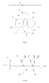
BACKGROUND OF THE INVENTION
Field of the Invention
The present invention relates to touch sensitive devices, in particular to a capacitive touch panel and a method for producing the same.
Description of the Related Art
Touch panels have been developed rapidly since their first emergence, and now the touch panels are widely applied to varieties of appliances, such as LCD monitors, cell phones, game machines, and so on.
Now, there are many kinds of touch panels, and capacitive-type touch panels are the most popular use in the market. A conventional capacitive touch panel generally includes a cover substrate for protection, two capacitive sensing layers spaced from each other by an insulation medium, and two fabrication substrates supporting each of the capacitive sensing layers respectively. Such construction at least has three substrates for different functions, but that would make the touch panel become very thick.
One way to minimize the thickness of the capacitive touch panel is to use a single capacitive sensing layer in the touch panel. FIG. 37 illustrates a schematic plan view of a conductor pattern structure of a conventional capacitive touch panel. The conductor pattern structure is a single conductive layer including first-axis conductor assemblies (such as first-axis conductor assembly 22) and second-axis conductor assemblies (such as second-axis conductor assembly 24). The single conductive layer is superposed on a cover substrate 10 directly instead of on a fabrication substrate.
The first-axis conductor assembly 22 includes adjacent conductor cells (such as conductor cells 222, 224 shown in FIG. 37) connected by conduction lines (such as conduction line 226). The second-axis conductor assembly 24 also includes adjacent conductor cells (such as conductor cells 242, 244 shown in FIG. 37) connected by conduction lines (such as conduction line 246). There are insulation layers (like insulation layer 30 shown in FIG. 37) set between the conduction lines of the first-axis conductor assemblies and the conduction lines of the second-axis conductor assemblies. But in such arrangement of the conductor assemblies, there are gaps (like gap 112) between the first-axis conductor assemblies and the second-axis conductor assemblies.
FIG. 38 is a schematic principle view showing the light transmitting path taken along a cross-section line A-A′ in FIG. 37. Parts of incident rays from outside (like incident rays 102) are only reflected from the surface of the cover substrate 10, generating reflected rays 104. Parts of incident rays from outside (like incident rays 106) are reflected from both the surface of the cover substrate 10 and the surface of the conductor assemblies (such as conductor assemblies 224 shown in FIG. 37), generating reflected rays 108 and reflected rays 110.
The cover substrate 10 and the conductive layer are made from different materials, for example, the cover substrate 10 is made from glass and the conductive layer is made from ITO (indium tin oxide), so the refractive index of the cover substrate 10 is different from that of the conductive layer. Thus the different ways that the reflected rays are generated from different part of the touch panel will make the two layer look different and let users readily see the conductor assemblies under the cover substrate.
Thus, it is desired to provide a capacitive touch panel having a single capacitive sensing layer that overcomes the above drawbacks of the conventional capacitive touch panel.
SUMMARY OF THE INVENTION
In one aspect, a capacitive touch panel is provided including a singular substrate; a mask layer formed on a border region of the singular substrate; a capacitive sensing layer comprising a plurality of first-axis conductor assemblies and a plurality of second-axis conductor assemblies, wherein the singular substrate, the mask layer and the capacitive sensing layer are integrally formed; and insulated auxiliary medium filled in gaps between the first-axis conductor assemblies and the second-axis conductor assemblies, wherein the refractive index of the auxiliary medium matches the refractive index of the capacitive sensing layer.
In another aspect, a method for producing a capacitive touch panel is provided including the following steps: providing a singular substrate; disposing a capacitive sensing layer on the singular substrate, the capacitive sensing layer including a plurality of first-axis conductor assemblies and second-axis conductor assemblies defining gaps between the first-axis conductor assemblies and second-axis conductor assemblies; and filling auxiliary materials in the gaps, the auxiliary materials having a refractive index matching a refractive index of the capacitive sensing layer.
Thus, the capacitive touch panel and method can make the capacitive touch panel with a single sensing layer have a uniform appearance and looks more attractive.
BRIEF DESCRIPTION OF THE DRAWINGS
FIG. 1 is a schematic plan view of a capacitive touch panel according to a first embodiment of the present invention;
FIG. 2 is a schematic principle view of the light transmitting path taken along a cross-section line B-B′ in FIG. 1;
FIG. 3 is a schematic plan view of a raw structure from a capacitive touch panel according to a first preferred embodiment of the present invention;
FIG. 4 is a schematic cross-sectional view taken along a cross-section line D-D′ in FIG. 3;
FIG. 5 is a schematic plan view of a raw structure from a capacitive touch panel with a fill-in form;
FIG. 6 is a schematic cross-sectional view taken along a cross-section line E-E′ in FIG. 5
FIG. 7 is a schematic plan view of a raw structure from a capacitive touch panel with a fill-out form;
FIG. 8 is a schematic cross-sectional view taken along a cross-section line F-F′ in FIG. 7
FIG. 9 is a schematic plan view of a raw structure from a capacitive touch panel with a contact hole form;
FIG. 10 is a schematic cross-sectional view taken along a cross-section line G-G′ in FIG. 9;
FIG. 11 shows how to fill a gap by the aerosol jetting printing;
FIG. 12 shows how to fill the gap by ink jetting printing;
FIG. 13 shows how to fill the gap by photolithography;
FIG. 14 is a schematic cross-sectional view taken along the cross-section line C-C′ in FIG. 1 according to a second embodiment of the present invention;
FIG. 15 is schematic cross-sectional view taken along the cross-section line C-C′ in FIG. 1 according to a second preferred embodiment of the present invention;
FIG. 16 is a schematic cross-sectional view taken along the cross-section line C-C′ in FIG. 1 according to a third embodiment of the present invention;
FIG. 17 is a schematic cross-sectional view taken along the cross-section line C-C′ in FIG. 1 according to a third preferred embodiment of the present invention;
FIG. 18 is a schematic cross-sectional view taken along the cross-section line C-C′ in FIG. 1 according to an alternative of the third embodiment of the present invention;
FIG. 19 is a schematic cross-sectional view taken along the cross-section line C-C′ in FIG. 1 according to another alternative of the third embodiment of the present invention;
FIG. 20 is a schematic cross-sectional view taken along the cross-section line C-C′ in FIG. 1 according to a forth embodiment of the present invention;
FIG. 21 is a schematic cross-sectional view taken along the cross-section line C-C′ in FIG. 1 according to a forth preferred embodiment of the present invention;
FIG. 22 is a schematic cross-sectional view taken along the cross-section line C-C′ in FIG. 1 according to an alternative of the forth embodiment of the present invention;
FIG. 23 is a schematic cross-sectional view taken along the cross-section line C-C′ in FIG. 1 according to another alternative of the forth embodiment of the present invention;
FIG. 24 is a schematic cross-sectional view taken along the cross-section line C-C′ in FIG. 1 according to a fifth embodiment of the present invention;
FIG. 25 is a schematic cross-sectional view taken along the cross-section line C-C′ in FIG. 1 according to a fifth preferred embodiment of the present invention;
FIG. 26 is a schematic cross-sectional view taken along the cross-section line C-C′ in FIG. 1 according to a fifth alternative embodiment of the present invention;
FIG. 27 is a schematic cross-sectional view taken along the cross-section line C-C′ in FIG. 1 according to a sixth embodiment of the present invention;
FIG. 28 is a schematic cross-sectional view taken along the cross-section line C-C′ in FIG. 1 according to a sixth preferred embodiment of the present invention;
FIG. 29 is a schematic cross-sectional view taken along the cross-section line C-C′ in FIG. 1 according to a sixth alternative embodiment of the present invention;
FIG. 30 is a schematic cross-sectional view taken along the cross-section line C-C′ in FIG. 1 according to a seventh embodiment of the present invention;
FIG. 31 is a schematic cross-sectional view taken along the cross-section line C-C′ in FIG. 1 according to a seventh alternative embodiment of the present invention;
FIG. 32 is a schematic cross-sectional view taken along the cross-section line C-C′ in FIG. 1 according to an eighth embodiment of the present invention;
FIG. 33 is a schematic cross-sectional view taken along the cross-section line C-C′ in FIG. 1 according to an eighth alternative embodiment of the present invention;
FIG. 34 is a schematic cross-sectional view taken along the cross-section line C-C′ in FIG. 1 according to a ninth embodiment of the present invention;
FIG. 35 is a schematic cross-sectional view taken along the cross-section line C-C′ in FIG. 1 according to a ninth alternative embodiment of the present invention;
FIG. 36 is a schematic cross-sectional view taken along the cross-section line C-C′ in FIG. 1 according to a ninth preferred embodiment of the present invention;
FIG. 37 illustrates a schematic plan view of a conductor pattern structure of a conventional capacitive touch panel; and
FIG. 38 is a principle view showing the light transmitting path taken along a cross-section line A-A′ in FIG. 34.
DETAILED DESCRIPTION
The detailed description of the present invention will be discussed in the following embodiments, which are not intended to limit the scope of the present invention, but can be adapted for other applications. While drawings are illustrated in details, it is appreciated that the quantity of the disclosed components may be greater or less than that disclosed, except expressly restricting the amount of the components.
With reference to FIG. 1 which is a schematic plan view of a capacitive touch panel according to a first embodiment of the present invention, the capacitive touch panel includes a singular substrate 40, a mask layer 50 formed on a border region of the singular substrate 40 and a capacitive sensing layer mostly formed on the middle region that is surrounded by the border region of the singular substrate 40. The singular substrate 40, the mask layer 50 and the capacitive sensing layer are integrally formed. The singular substrate 40 in the present invention could be as a cover substrate for protecting the capacitive sensing layer and a fabrication substrate for supporting the capacitive sensing layer. The mask layer 50 is used for covering the internal structures at the border region of the touch panel and generally includes but not limited to black matrices. In a preferred embodiment, the middle region is a view area of the singular substrate 40.
The capacitive sensing layer includes a plurality of parallel first-axis conductor assemblies (like first-axis conductor assembly 62) and a plurality of second-axis conductor assemblies (like second-axis conductor assembly 64) perpendicular to the first-axis conductor assemblies. Each first-axis conductor assembly includes a plurality of equally-spaced first-axis conductor cells (like first-axis conductor cell 622), each second-axis conductor assembly includes a plurality of equally-spaced second-axis conductor cells (like second-axis conductor cell 642). The shape of the first-axis conductor cells and second-axis conductor cells may be hexagon, diamond or other polygons. The first-axis conductor cells and second-axis conductor cells are separated from each other, forming gaps between the first-axis conductor cells and second-axis conductor cells. The width of the gaps is approximate 30 μm. The capacitive touch panel further includes auxiliary medium 80 filled in the above gaps, the refractive index of the auxiliary medium 80 matches the refractive index of the capacitive sensing layer, so that the capacitive sensing layer can not be seen by users.
For transmitting touch signals, adjacent conductor cells in a same axis are connected by conduction lines (like conduction line 624 in the first-axis assembly and conduction line 644 in the second-axis assembly). The auxiliary medium 80 is insulative and also used to cover the conduction lines 644 so that the conduction lines 622 are insulated from the conduction lines 644.
FIG. 2 shows a schematic principle view of the light transmitting path taken along the cross-section line B-B′ in FIG. 1. Incident rays 410, for example, are firstly reflected from the surface of the singular substrate 40, generating reflected rays 412 and then being refracted, secondly reflected from the surface of the gap area filled with the auxiliary medium 80, generating reflected rays 414. Incident rays 420 are firstly reflected from the surface of the singular substrate 40, generating reflected rays 422 and then being refracted, secondly reflected from the surface of the conductor assemblies, more detailed, from the surface of a conductor cell 622 of the conductor assembly shown in FIG. 2, generating reflected rays 424. Since the refractive index of the auxiliary medium 80 matches that of the capacitive sensing layer, wherever the incident point is, the incident rays are reflected in the same way. Thus, the touch panel has a uniform appearance, and users can not distinguish the gaps and the conductor assemblies easily, which will prettify the appearance of the touch panel.
Furthermore, the auxiliary medium 80 is formed between the conduction lines 624 and 644, so the conduction lines 622 are insulated from the conduction lines 644. Compared to the conventional touch panels that use insulated layers to implement the above insulating property, the auxiliary medium 80 in the present invention can be used as the insulated layers between the conduction lines 624 and 644, and also can be used as an index-matching layer for those gap areas. Thus, the process of making the touch panel is simplified.
In a preferred embodiment, the refractive index of the auxiliary medium is 1.5˜2.1, and the capacitive sensing layer may be made from ITO with refractive index 1.7˜1.8. The auxiliary medium is made from transparent materials selected from the group consisting of SiO2 with refractive index 1.5˜1.6, TiO2 with refractive index 1.7˜1.8, Nb2O5 with refractive index 2.0˜2.1 and transparent insulating resistance with refractive index 1.5˜1.6. The capacitive sensing layer is single layered and directly formed on the singular substrate 40, so there is no need to provide two conventional fabrication substrates for supporting the capacitive sensing layer, consequently the thickness of the whole touch panel will be reduced.
According to the present invention, the auxiliary medium 80 is filled in the gaps. The filling process can be implemented by many ways, such as aerosol jet printing, ink jet printing and photolithography. FIG. 3 is a schematic plan view of a raw structure of a part taken from a capacitive touch panel according to the first preferred embodiment of the present invention, and FIG. 4 is a schematic cross-sectional view taken along the cross-section line D-D′ in FIG. 3. The first-axis conductor assemblies 69 and the second-axis conductor assemblies 67 of the capacitive touch panel are formed on the singular substrate 40 and include square shaped conductor cells, the conductor cells 692, 694 arranged along the first-axis are not connected, and the conductor cells 672, 674 arranged along the second-axis are electrically connected by a conduction line 676. Conductor cells 672,674 and conductor cells 692,694 are separated from each other, forming gaps between them.
After the gaps being filled with the auxiliary medium 80, there are three kinds of filling forms: fill-in, fill-out and contact hole. In the fill-in form, the auxiliary medium 80 can be fit to fill the gaps properly, without spilling from the gaps, as FIG. 5 shows. The auxiliary medium 80 is also formed on the conduction line 676. FIG. 6 is a schematic cross-sectional view taken along the cross-section line E-E′ in FIG. 5. In the fill-out form, the auxiliary medium 80 may spill from the gaps and covers part of the conductor cells, as FIG. 7 shows. FIG. 8 is a schematic cross-sectional view taken along the cross-section line F-F′ in FIG. 7. In the contact hole forms, as FIG. 9 shows, the auxiliary medium 80 covers almost the whole sensing layer. At least two contact holes 696 are formed in the auxiliary medium 80 for connecting the two conductor cells 692, 694. FIG. 10 is a schematic cross-sectional view taken along the cross-section line G-G′ in FIG. 9.
There are three ways to fill the gaps with the auxiliary medium. FIG. 11 shows how to fill a gap by the aerosol jetting printing. A touch sensing layer 2 including a gap is formed on a substrate 1. Aerosol jetting printing consists of the step of directing a focused stream of atomized particles towards a substrate. The high velocity of the stream causes the particles to impact on the substrate. Thermal post processing is usually required to sinter the particles together to adhere them to the substrate. The particles are far too small (about 10 μm) compared to the width of gaps.
FIG. 12 shows how to fill the gap by an ink jetting printing. Ink jetting printing works by propelling individual small droplets of ink towards a substrate. The ink is forced through a small orifice by a variety of means including pressure, heat, and vibration. The liquid droplets usually have diameters bigger than 30 μm.
FIG. 13 shows how to fill the gap by photolithography. The method firstly forms an auxiliary medium 3 with insulating property and having nearly the same size as the singular substrate 40 on the capacitive sensing layer 2, secondly etches the auxiliary medium 3 by photolithography, only leaving the auxiliary medium filled in the gaps. Mask 4 must be precisely aligned to the gaps and irradiated by light 5 in order to form the auxiliary medium filled in the gaps properly. Because the auxiliary medium 3 forms on the conduction lines as well, another process of forming an insulated layer on the conduction lines can be reduced in this filling process.
After the above filling process, the conductor cells 622 arranged along the first-axis are then electrically connected by conduction lines 624 that cross and insulate with the conduction lines 644, as shown in FIG. 1. The conduction lines 624 can be metal lines or transparent conductive lines. The connection may be implemented by direct contact or contact holes.
Referring to FIG. 1, each conductor assembly is electrically connected to a signal transmission line (like signal transmission line 90) in the border region of the singular substrate 40. The connection can be implemented by adopting at least one way selected from the following: connecting via contact holes, connecting by direct contact and electrically connecting without contact.
In the way of connecting a conductor assembly to a signal transmission line via a contact hole, the contact hole is formed in the mask layer 50.
Referring to FIG. 14, which is a schematic cross-sectional view taken along the cross-section line C-C′ in FIG. 1 according to a second embodiment of the present invention. The mask layer 50 covers part of the conductor assembly 66. The contact hole 502 is formed in the mask layer 50. The signal transmission line 90 passes through the contact hole 502 and one end of the signal transmission line 90 contacts the conductor assembly 66.
FIG. 15 is a schematic cross-sectional view taken along the cross-section line C-C′ in FIG. 1 according to the second preferred embodiment of the present invention. In this embodiment, the mask layer 50 covers the signal transmission line 90, the contact hole 502 is formed in the mask layer 50. The conductor assembly 66 passes through the contact hole 502 and one end of the conductor assembly 66 contacts the signal transmission line 90. There may be more contact holes in the mask layer 50, and the shape of each contact hole may be rectangular, circular or polygon.
In the way of connecting a conductor assembly to a signal transmission line by direct contact, the conductor assembly directly contacts the signal transmission line.
Referring to FIG. 16, which is a schematic cross-sectional view taken along the cross-section line C-C′ in FIG. 1 according to a third embodiment of the present invention. The conductor assembly 66 directly contacts the signal transmission line 90 and both of the conductor assembly 66 and the signal transmission line 90 are covered by the mask layer 50 in the border region, wherein the signal transmission line 90 overlaps the conductor assembly 66.
FIG. 17 is a schematic cross-sectional view taken along the cross-section line C-C′ in FIG. 1 according to the third preferred embodiment of the present invention, the partial conductor assembly 66 and the signal transmission line 90 are successively covered by a transparent dielectric layer 52 and mask layer 50 in case the mask layer 50 being conductive, wherein the signal transmission line 90 overlaps the conductor assembly 66.
FIG. 18 is a schematic cross-sectional view taken along the cross-section line C-C′ in FIG. 1 according to an alternative of the third embodiment of the present invention, in this embodiment, the contact has other forms. The conductor assembly 66 directly contacts the signal transmission line 90. Both the conductor assembly 66 and the signal transmission line 90 are covered by the mask layer 50 in the border region, wherein the conductor assembly 66 overlaps the signal transmission line 90. The transparent dielectric layer 52 also can be added above the conductor assembly 66 and the signal transmission line 90 and under the mask layer 50 in case the mask layer 50 being conductive, the dielectric layer 52 covers both the partial conductor assembly 66 and the signal transmission line 90 and is disposed under the mask layer 50, as FIG. 19 shows.
The difference between the embodiments shown in FIG. 16 and FIG. 18 and the difference between the embodiments shown in FIG. 17 and FIG. 19 are the forming sequence of the conductor assembly 66 and the signal transmission line 90, wherein as shown in FIG. 16 and FIG. 18, the conductor assembly 66 firstly is formed on the singular substrate 40 and then the signal transmission line 90 is formed to overlap part of the conductor assembly 66, and as shown in FIG. 18 and FIG. 19, the signal transmission line 90 firstly is formed on the singular substrate 40 and then the conductor assembly 66 is formed to overlap part of the signal transmission line 90.
Referring to FIG. 20, which is a schematic cross-sectional view taken along the cross-section line C-C′ in FIG. 1 according to a forth embodiment of the present invention. The conductor assembly 66 directly contacts the signal transmission line 90 and both are arranged over the mask layer 50 in the border region, wherein the signal transmission line 90 overlaps the conductor assembly 66. FIG. 21 is a schematic cross-sectional view taken along the cross-section line C-C′ in FIG. 1 according to the forth preferred embodiment of the present invention, the conductor assembly 66 and the signal transmission line 90 are arranged over a transparent dielectric layer 52 that covers the mask layer 50 in case the mask layer 50 being conductive.
FIG. 22 is a schematic cross-sectional view taken along the cross-section line C-C′ in FIG. 1 according to an alternative of the forth embodiment of the present invention. The conductor assembly 66 directly contacts the signal transmission line 90. Both the conductor assembly 66 and signal transmission line 90 are arranged over the mask layer 50 in the border region, wherein the conductor assembly 66 overlaps the signal transmission line 90 and is placed over the signal transmission line 90. The transparent dielectric layer 52 also can be added above the mask layer 50 to isolate the conductor assembly 66 and the signal transmission line 90 from the mask layer 50 in case the mask layer 50 being conductive, as FIG. 23 shows.
The difference between the embodiments shown in FIG. 20 and FIG. 22 and the difference between the embodiments shown in FIG. 21 and FIG. 23 are the forming sequence of the conductor assembly 66 and the signal transmission line 90.
In other embodiments, all the direct contact between the conductor assembly 66 and the signal transmission line 90 can be in the view area other than the border region. FIG. 24 is a schematic cross-sectional view taken along the cross-section line C-C′ in FIG. 1 according to a fifth embodiment of the present invention. The conductor assembly 66 is placed on the singular substrate 40, the mask layer 50 overlaps the conductor assembly 66, part of the signal transmission line 90 directly contacts the conductor assembly 66 in the view area and the other part of the signal transmission line 90 overlaps the mask layer 50 in the border area. At the base of the fifth embodiment, as FIG. 25 shows, a transparent dielectric layer 52 is disposed between the conductor assembly 66 and the mask layer 50 in case the mask layer 50 being conductive. Alternately, as FIG. 26 shows, the transparent dielectric layer 52 is disposed between the mask layer 50 and the signal transmission line 90 in case the mask layer 50 being conductive.
FIG. 27 is a schematic cross-sectional view taken along the cross-section line C-C′ in FIG. 1 according to a sixth embodiment of the present invention. The signal transmission line 90 is disposed on the singular substrate 40, part of the signal transmission line 90 is in the border region and covered by the mask layer 50, the other part of the signal transmission line 90 is in the view area and covered by the conductor assembly 66. The conductor assembly 66 directly contacts the signal transmission line 90 is in the view area and overlaps the mask layer 50 in the border region. At the base of the sixth embodiment, as FIG. 28 shows, a transparent dielectric layer 52 is disposed between the mask layer 50 and the signal transmission line 90 in case the mask layer 50 being conductive. Alternately, as FIG. 29 shows, the transparent dielectric layer 52 is disposed between the conductor assembly 66 and the mask layer 50 in case the mask layer 50 being conductive.
In the above embodiments, the material of the transparent dielectric layer is selected from the group consisting of silicon, silicon oxide and silicon nitride.
In the way of connecting a conductor assembly to a signal transmission line without contact, the conductor assembly is separated from the signal transmission line by the mask layer. FIG. 30 is a schematic cross-sectional view of a seventh embodiment of the present invention. The signal transmission line 90 is completely covered by the mask layer 50, the conductor assembly 66 overlaps the mask layer 50 where the overlapped part of the mask layer 50 also contacts the signal transmission line 90. The mask layer 50 may be made of aeolotropic materials, that is, the mask layer 50 are conductive in specified direction (such in Y direction) because the resistivity of the mask layer 50 in the X direction or in other directions is still high, the mask layer 50 can be regarded as non-conductive in these non-specified directions. In this embodiment, the mask layer 50 conducts in the direction of connecting the conductor assembly 66 and the signal transmission line 90 so that the conductor assembly 66 can electrically connect to the signal transmission line 90 by the mask layer 50.
In an alternative embodiment, as FIG. 31 shows, part of the conductor assembly 66 is covered by the mask layer 50; the signal transmission line 90 is placed isolate over the mask layer 50. The conductor assembly 66, mask layer 50 and the signal transmission line 90 have common overlapped parts with conduction due to the mask layer 50 may be made of aeolotropic materials.
Two or more kinds of above mentioned connecting way can be used together. FIG. 32 is a schematic cross-sectional view taken along the cross-section line C-C′ in FIG. 1 according to an eighth embodiment of the present invention. The conductor assembly 66 is disposed on the singular substrate 40, the mask layer 50 overlaps the conductor assembly 66 with the overlapped part having contact holes 502. The signal transmission line 90 directly contacts the conductor assembly 66 by being directly disposed on the conductor assembly 66 as well as passing through the contact holes 502 to contact the conductor assembly 66. FIG. 33 is an alternative schematic cross-sectional view taken along the cross-section line C-C′ in FIG. 1 according to an eighth embodiment of the present invention. The signal transmission line 90 is formed on the singular substrate 40, the mask layer 50 overlaps the signal transmission line 90 with the overlapped part having contact holes 502, The conductor assembly 66 contacts the signal transmission line 90 by being directly disposed on the part of the transmission line 90 that is not covered by the mask layer 50. The conductor assembly 66 also passes through the contact holes 502 to contact the part of the signal transmission line 90 that is covered by the mask layer 50. The difference between the embodiments shown in FIG. 32 and FIG. 33 is the forming sequence of the conductor assembly 66 and the signal transmission line 90.
All the above described embodiments are single-side configurations, that is, the mask layer, conductor assemblies, signal transmission lines, etc. are disposed on only one side of the singular substrate 40. Besides the single-side configurations, there are double-sides configurations.
Referring to FIG. 34 which is an alternative schematic cross-sectional view taken along the cross-section line C-C′ in FIG. 1 according to a ninth embodiment of the present invention, the conductor assembly 66 and the signal transmission line 90 are disposed on one side of the singular substrate 40, and the mask layer 50 corresponding to a border region is disposed on the other side of the singular substrate 40. A transparent passivation layer 402 is formed on the singular substrate 40 with the same side of the mask layer 50 and also covers the mask layer 50. The transparent passivation layer 402 is used for anti-glare and/or anti-reflection. The conductor assembly 66 connects to the signal transmission line 90 by direct contact, which is illustrated as the conductor assembly 66 overlapping the signal transmission line 90.
Alternately, the conductor assemblies may be disposed on both sides of the singular substrate 40 s, as FIG. 35 shows. FIG. 35 is a schematic cross-sectional view taken along the cross-section line C-C′ in FIG. 1 according to a ninth alternative embodiment of the present invention. The conductor assembly 66A and the signal transmission line 90 are disposed on one side of the singular substrate 40, and a conductor assembly 66B is disposed on the other side of the singular substrate 40. The conductor assembly 66B extends to a border region and is overlapped by the mask layer 50. A transparent passivation layer 402 is formed with the same side of the mask layer 50 and covers the conductor assembly 66B and the mask layer 50. The conductor assembly 66A connects to the signal transmission line 90 by direct contact, which is illustrated as the conductor assembly 66A overlapping the signal transmission line 90. In a preferred embodiment, a transparent dielectric layer 52 may be added between the mask layer 50 and the conductor assembly 66B in case the mask layer 50 being conductive, as FIG. 36 shows.
In the above double side configurations, the direct contact form is: the conductor assembly 66 overlapping the signal transmission line 90. In fact, the direct contact form also can be: the signal transmission line 90 overlapping the conductor assembly 66.
The material of the capacitive sensing layer is selected from the group consisting of ITO, TCO, conductive polymer, CNTs, and other similar materials. The material of the mask layer is selected from the group consisting of black photoresist, black resin, black ink, and other similar material with other colors.
Although the invention has been described in language specific to structural features and/or methodological acts, it is to be understood that the invention defined in the appended claims is not necessarily limited to the specific features or acts described. Rather, the specific features and acts are disclosed as example forms of implementing the claimed invention.

Claims (26)

What is claimed is:
1. A capacitive touch panel, comprising:
a singular substrate;
a mask layer formed on a border region of the singular substrate;
a capacitive sensing layer comprising:
a plurality of first-axis conductor assemblies; and
a plurality of second-axis conductor assemblies, wherein:
each first-axis conductor assembly of the plurality of first-axis conductor assemblies has a plurality of first-axis conductor cells and each second-axis conductor assembly of the plurality of second-axis conductor assemblies has a plurality of second-axis conductor cells,
the plurality of first-axis conductor cells and the plurality of second-axis conductor cells are formed on a same layer of the singular substrate,
the mask layer and the capacitive sensing layer are integrally formed,
a gap is defined between a first sidewall of a first first-axis conductor cell of the plurality of first-axis conductor cells and a second sidewall of a first second-axis conductor cell of the plurality of second-axis conductor cells, the second sidewall facing the first sidewall,
a contact hole is formed in the mask layer,
a signal transmission line in the border region passes through the contact hole, and
one end of the signal transmission line contacts a conductor assembly of one of the plurality of first-axis conductor assemblies or one of the plurality of second-axis conductor assemblies; and
an insulated auxiliary medium filling the gap, wherein:
the insulated auxiliary medium extends from a first edge of the first first-axis conductor cell at which the first sidewall intersects a third sidewall of the first first-axis conductor cell to a second edge of the first first-axis conductor cell at which the first sidewall intersects a fourth sidewall of the first first-axis conductor cell, and
a refractive index of the insulated auxiliary medium matches a refractive index of the capacitive sensing layer.
2. The capacitive touch panel according to claim 1, wherein the singular substrate is a cover substrate for protecting the capacitive sensing layer and a fabrication substrate for supporting the capacitive sensing layer.
3. The capacitive touch panel according to claim 1, wherein the mask layer comprises black matrices.
4. The capacitive touch panel according to claim 1, wherein the insulated auxiliary medium is selected from the group consisting of SiO2 and TiO2.
5. The capacitive touch panel according to claim 1, wherein the insulated auxiliary medium is a transparent insulating material.
6. The capacitive touch panel according to claim 1, wherein the plurality of first-axis conductor cells are equally spaced, the plurality of second-axis conductor cells are equally spaced, adjacent conductor cells in a same axis are connected by conduction lines, and the insulated auxiliary medium covers the conduction lines extending along a second-axis.
7. The capacitive touch panel according to claim 1, wherein the conductor assembly of one of the plurality of first-axis conductor assemblies or one of the plurality of second-axis conductor assemblies directly contacts the signal transmission line in the border region and both the conductor assembly and the signal transmission line are covered by the mask layer in the border region.
8. The capacitive touch panel according to claim 7, wherein the conductor assembly and the signal transmission line are successively covered by a transparent dielectric layer and the mask layer.
9. The capacitive touch panel according to claim 8, wherein a material of the transparent dielectric layer is selected from a group consisting of silicon, silicon oxide and silicon nitride.
10. The capacitive touch panel according to claim 1, wherein the conductor assembly of one of the plurality of first-axis conductor assemblies or one of the plurality of second-axis conductor assemblies directly contacts the signal transmission line in the border region and both the conductor assembly and the mask layer are covered by the signal transmission line.
11. The capacitive touch panel according to claim 10, wherein the conductor assembly is covered by a transparent dielectric layer disposed under the mask layer.
12. The capacitive touch panel according to claim 1, wherein the mask layer is aeolotropic and disposed sot between the conductor assembly of one of the plurality of first-axis conductor assemblies or one of the plurality of second-axis conductor assemblies and the signal transmission line in the border region.
13. The capacitive touch panel according to claim 2, wherein each conductor assembly of the plurality of first-axis conductor assemblies and the plurality of second-axis conductor assemblies is connected to part of the signal transmission line in a view area of the singular substrate by direct contact.
14. The capacitive touch panel according to claim 1, wherein each conductor assembly of the plurality of first-axis conductor assemblies and the plurality of second-axis conductor assemblies is connected to the signal transmission line in the border region as a double side configuration comprising:
the conductor assembly; and
the signal transmission line being disposed on a first-side of the singular substrate, the mask layer corresponding to the border region being disposed on a second-side of the singular substrate opposite the first side, and a transparent passivation layer being formed on the singular substrate from the second side and also covering the mask layer.
15. The capacitive touch panel according to claim 1, wherein each conductor assembly of the plurality of first-axis conductor assemblies and the plurality of second-axis conductor assemblies is connected to the signal transmission line in the border region as a double side configuration comprising:
the conductor assembly; and
the signal transmission line being disposed on a first side of the singular substrate, the conductor assembly being disposed on a second side of the singular substrate opposite the first side, the conductor assembly extending to the border region and being overlapped by the mask layer, and a transparent passivation layer being formed on the second side and covering the conductor assembly and the mask layer.
16. The capacitive touch panel according to claim 15, further comprising a transparent dielectric layer between the mask layer and the conductor assembly.
17. The capacitive touch panel according to claim 1, wherein a material of the capacitive sensing layer is selected from a group consisting of indium tin oxide (ITO), transparent conductive oxide (TCO), conductive polymer and carbon nanotube (CNTs).
18. The capacitive touch panel according to claim 1, wherein a material of the mask layer is selected from a group consisting of black photoresist, black resin and black ink.
19. The capacitive touch panel according to claim 1, wherein the conductor assembly of one of the plurality of first-axis conductor assemblies or one of the plurality of second-axis conductor assemblies directly contacts the signal transmission line in the border region and wherein both the mask layer and the signal transmission line are covered by the conductor assembly.
20. The capacitive touch panel according to claim 19, wherein the signal transmission line is covered by a transparent dielectric layer disposed under the mask layer.
21. The capacitive touch panel according to claim 1, wherein:
each first-axis conductor cell of the plurality of first-axis conductor cells has a first surface facing the singular substrate and a second surface opposite to the first surface,
each second-axis conductor cell of the plurality of second-axis conductor cells has a third surface facing the singular substrate and a fourth surface opposite to the third surface, and
the insulated auxiliary medium is disposed on a surface of the singular substrate without covering the second surface and the fourth surface.
22. The capacitive touch panel according to claim 1, wherein the insulated auxiliary medium is disposed on a surface of the singular substrate covering edges of the plurality of first-axis conductor cells and the plurality of second-axis conductor cells.
23. The capacitive touch panel according to claim 1, wherein:
each first-axis conductor cell of the plurality of first-axis conductor cells has a first surface facing the singular substrate and a second surface opposite to the first surface, and
the insulated auxiliary medium overlies a majority of the second surface.
24. The capacitive touch panel according to claim 1, wherein the insulated auxiliary medium is a homogeneous material.
25. The capacitive touch panel according to claim 1, wherein the insulated auxiliary medium is selected from a group consisting of SiO2 (silicon oxide) with a refractive index of about 1.5 to 1.6, TiO2 (titanium dioxide) with a refractive index of about 1.7 to 1.8, Nb2O5 (Niobium pentoxide) with a refractive index of about 2.0 to 2.1 and a transparent insulating material with a refractive index of about 1.5 to 1.6.
26. A capacitive touch panel, comprising:
a singular substrate;
a mask layer formed on a border region of the singular substrate;
a capacitive sensing layer comprising:
a plurality of first-axis conductor assemblies; and
a plurality of second-axis conductor assemblies, wherein:
each first-axis conductor assembly of the plurality of first-axis conductor assemblies has a plurality of first-axis conductor cells and each second-axis conductor assembly of the plurality of second-axis conductor assemblies has a plurality of second-axis conductor cells,
the plurality of first-axis conductor cells and the plurality of second-axis conductor cells are formed on a same layer of the singular substrate,
the mask layer and the capacitive sensing layer are integrally formed,
a gap is defined between a first sidewall of a first first-axis conductor cell of the plurality of first-axis conductor cells and a second sidewall of a first second-axis conductor cell of the plurality of second-axis conductor cells, the second sidewall facing the first sidewall,
a contact hole is formed in the mask layer,
a conductor assembly of one of the plurality of first-axis conductor assemblies or one of the plurality of second-axis conductor assemblies passes through the contact hole, and
one end of the conductor assembly contacts a signal transmission line in the border region; and
an insulated auxiliary medium filling the gap, wherein:
the insulated auxiliary medium extends from a first edge of the first first-axis conductor cell at which the first sidewall intersects a third sidewall of the first first-axis conductor cell to a second edge of the first first-axis conductor cell at which the first sidewall intersects a fourth sidewall of the first first-axis conductor cell, and
a refractive index of the insulated auxiliary medium matches a refractive index of the capacitive sensing layer.
US12/942,037 2010-11-09 2010-11-09 Capacitive touch panel and method for producing the same Expired - Fee Related US9563315B2 (en)

Priority Applications (6)

Application Number Priority Date Filing Date Title
US12/942,037 US9563315B2 (en) 2010-11-09 2010-11-09 Capacitive touch panel and method for producing the same
KR1020110036979A KR101322383B1 (en) 2010-11-09 2011-04-20 Capactive touch panel and method for producing the same
TW100116186A TWI467449B (en) 2010-11-09 2011-05-09 Capacitive touch panel and method for producing the same
TW100208334U TWM415362U (en) 2010-11-09 2011-05-10 Capacitive touch panel
CN201110121617.5A CN102467309B (en) 2010-11-09 2011-05-11 Capacitive type touch pad and manufacture method thereof
CN2011201492503U CN202084024U (en) 2010-11-09 2011-05-11 Capacitive touch board

Applications Claiming Priority (1)

Application Number Priority Date Filing Date Title
US12/942,037 US9563315B2 (en) 2010-11-09 2010-11-09 Capacitive touch panel and method for producing the same

Publications (2)

Publication Number Publication Date
US20120113042A1 US20120113042A1 (en) 2012-05-10
US9563315B2 true US9563315B2 (en) 2017-02-07

Family

ID=45344647

Family Applications (1)

Application Number Title Priority Date Filing Date
US12/942,037 Expired - Fee Related US9563315B2 (en) 2010-11-09 2010-11-09 Capacitive touch panel and method for producing the same

Country Status (4)

Country Link
US (1) US9563315B2 (en)
KR (1) KR101322383B1 (en)
CN (2) CN102467309B (en)
TW (2) TWI467449B (en)

Cited By (1)

* Cited by examiner, † Cited by third party
Publication number Priority date Publication date Assignee Title
US20190064954A1 (en) * 2012-05-16 2019-02-28 Tpk Touch Solutions (Xiamen) Inc. Touch panel and touch sensing display using the same

Families Citing this family (39)

* Cited by examiner, † Cited by third party
Publication number Priority date Publication date Assignee Title
US8605050B2 (en) * 2007-08-21 2013-12-10 Tpk Touch Solutions (Xiamen) Inc. Conductor pattern structure of capacitive touch panel
TWI374379B (en) 2007-12-24 2012-10-11 Wintek Corp Transparent capacitive touch panel and manufacturing method thereof
WO2012061975A1 (en) * 2010-11-09 2012-05-18 Tpk Touch Solutions Inc. Touch panel device
CN102866794A (en) 2011-06-15 2013-01-09 宸鸿光电科技股份有限公司 Touch control sensing layer and manufacturing method thereof
TWI459255B (en) * 2011-08-04 2014-11-01 Innolux Corp Touch panel, touch display apparatus using the same and manufacturing method thereof
TWI588844B (en) * 2011-12-01 2017-06-21 創為精密材料股份有限公司 Etching-free conductive substrate structure for 4-wire type touch panel and manufacturing method thereof
TWI616901B (en) * 2011-12-01 2018-03-01 創為精密材料股份有限公司 Dielelectric substrate structure for 5-wire type touch panel and manufacturing method thereof
TWI616900B (en) * 2011-12-01 2018-03-01 創為精密材料股份有限公司 Dielectric substrate structure for 4-wire type touch panel and manufacturing method thereof
TWI588846B (en) * 2011-12-01 2017-06-21 創為精密材料股份有限公司 Conductive substrate structure for 5-wire type touch panel and manufacturing method thereof
CN103186272B (en) * 2011-12-29 2016-10-05 宸鸿科技(厦门)有限公司 Contact panel and manufacture method thereof
CN202404553U (en) * 2012-03-01 2012-08-29 祥达光学(厦门)有限公司 Touch screen structure with shielding metal line
CN103309527B (en) * 2012-03-15 2018-01-16 深圳市振宇达智能机器人科技有限公司 Capacitive type touch pad and its manufacturing equipment
CN103365453B (en) * 2012-04-06 2016-08-10 宸鸿科技(厦门)有限公司 Contact panel
US9262021B2 (en) * 2012-04-11 2016-02-16 Synaptics Incorporated Two layer capacitive sensor
TWI495930B (en) * 2012-05-15 2015-08-11 Wistron Corp Planar touch panel with single substrate
WO2013172055A1 (en) * 2012-05-17 2013-11-21 株式会社カネカ Substrate with transparent electrode, method for manufacturing same, and touch panel
CN103576950B (en) * 2012-07-24 2016-08-24 宸鸿科技(厦门)有限公司 Contact panel and preparation method thereof
CN103677357B (en) * 2012-09-06 2016-12-28 宸鸿科技(厦门)有限公司 For the covering plate structure of contact panel and manufacture method thereof and contact panel
CN103677459A (en) * 2012-09-25 2014-03-26 比亚迪股份有限公司 Capacitive touch screen and manufacturing method thereof
KR20140046946A (en) * 2012-10-11 2014-04-21 엘지이노텍 주식회사 Touch panel and method for manufacturing the same
CN102968232A (en) * 2012-11-23 2013-03-13 深圳莱宝高科技股份有限公司 Capacitive touch panel and production method thereof
CN103885578B (en) * 2012-12-20 2017-04-05 宸正光电(厦门)有限公司 Contact panel and its manufacture method
CN103970332B (en) * 2013-02-04 2017-07-28 宸鸿科技(厦门)有限公司 Contact panel and its manufacture method
CN104123022B (en) * 2013-04-24 2017-07-28 宸鸿科技(厦门)有限公司 Contact panel and its covering plate structure
CN104166472B (en) * 2013-05-19 2019-05-28 祥达光学(厦门)有限公司 Touch sensing device and preparation method thereof
KR101865685B1 (en) * 2013-05-23 2018-06-08 동우 화인켐 주식회사 Transparent electrode pattern structure and touch screen panel having the same
CN104216547B (en) * 2013-06-04 2017-12-01 宸鸿科技(厦门)有限公司 A kind of contact panel and its manufacture method
CN104298381B (en) * 2013-07-17 2017-07-11 宸鸿科技(厦门)有限公司 Contact panel, the optical match glue and previous building methods that are applied to contact panel
US9677168B2 (en) * 2013-10-08 2017-06-13 TPK America, LLC Touch panel and method for manufacturing the same
CN104765481B (en) * 2014-01-06 2019-05-28 宸鸿科技(厦门)有限公司 Touch panel and preparation method thereof
US20150253902A1 (en) * 2014-03-07 2015-09-10 Cn Innovations Limited Structure and the associated manufacturing process for a single-sided multi-layer mutual capacitance touch panel
CN103941911B (en) * 2014-03-07 2017-08-29 上海天马微电子有限公司 A kind of contact panel and display device
CN105335000A (en) * 2014-08-15 2016-02-17 群创光电股份有限公司 Touch display device
KR102256461B1 (en) * 2014-10-10 2021-05-26 삼성디스플레이 주식회사 Touch sensor and display including the same
TWI560838B (en) 2015-01-08 2016-12-01 Innolux Corp Touch device
CN105824446B (en) * 2015-01-08 2019-05-10 群创光电股份有限公司 Touch device
CN105988619B (en) * 2015-02-12 2019-08-13 宸鸿科技(厦门)有限公司 Show touch device
KR101727263B1 (en) 2015-09-09 2017-04-26 주식회사 하이딥 Touch pressure detectable touch input device including display module
CN108803908A (en) * 2017-04-26 2018-11-13 群创光电股份有限公司 Touch device

Citations (45)

* Cited by examiner, † Cited by third party
Publication number Priority date Publication date Assignee Title
US6137427A (en) 1994-04-05 2000-10-24 Binstead; Ronald Peter Multiple input proximity detector and touchpad system
US6188391B1 (en) 1998-07-09 2001-02-13 Synaptics, Inc. Two-layer capacitive touchpad and method of making same
US20010043046A1 (en) * 2000-05-08 2001-11-22 Takeshi Fukunaga Luminescent apparatus and method of manufacturing the same
US20040141110A1 (en) 2002-12-24 2004-07-22 Lg. Philips Lcd Co., Ltd. Single unit liquid crystal display touch panel and method of fabricating the same
US20040160424A1 (en) 2000-02-02 2004-08-19 3M Innovative Properties Company Touch screen panel with integral wiring traces
US6814452B2 (en) 2000-03-31 2004-11-09 Nissha Printing Co., Ltd. Touch-panel with light shielding peripheral part
US6819316B2 (en) 2001-04-17 2004-11-16 3M Innovative Properties Company Flexible capacitive touch sensor
US20050073507A1 (en) 2003-10-06 2005-04-07 Richter Paul J. Touch input sensing device
US20060274055A1 (en) 2005-06-01 2006-12-07 Synaptics Incorporated Touch pad with flexible substrate
US20060272850A1 (en) * 2005-06-06 2006-12-07 Matsushita Electric Industrial Co., Ltd. Interlayer connection conductor and manufacturing method thereof
US20070165004A1 (en) 2006-01-17 2007-07-19 World Properties, Inc. Capacitive touch sensor with integral EL backlight
TW200742610A (en) 2006-05-10 2007-11-16 Tpk Touch Solutions Inc Method of hiding transparent electrodes on a transparent substrate
US7339579B2 (en) 2003-12-15 2008-03-04 3M Innovative Properties Company Wiring harness and touch sensor incorporating same
US20080136791A1 (en) 2006-12-07 2008-06-12 Sony Ericsson Mobile Communications Ab Liquid resistive touch panel
US20080142352A1 (en) 2006-12-18 2008-06-19 Wright David G Two circuit board touch-sensor device
US20080165158A1 (en) 2007-01-05 2008-07-10 Apple Inc. Touch screen stack-ups
US20080165139A1 (en) * 2007-01-05 2008-07-10 Apple Inc. Touch screen stack-up processing
US20080264699A1 (en) * 2007-04-27 2008-10-30 Trendon Touch Technology Corp. Conductor pattern structure of capacitive touch panel
US20090091546A1 (en) * 2007-10-04 2009-04-09 Sun-Kyu Joo Display with touch screen panel and method of manufacturing the same
US20090102814A1 (en) 2007-10-19 2009-04-23 Tpo Displays Corp. Image displaying systems
US20090146967A1 (en) * 2007-12-05 2009-06-11 Sony Corporation Display apparatus
US20090160824A1 (en) * 2007-12-25 2009-06-25 Cando Corporation Sensory structure of touch panel
CN101504496A (en) 2009-03-04 2009-08-12 信利半导体有限公司 Touch screen and panel display module integrated combination module and method for producing the same
US20090207151A1 (en) * 2008-02-18 2009-08-20 Tpk Touch Solutions Inc. Capacitive Touch Panel
US20090278815A1 (en) * 2008-05-08 2009-11-12 Wintek Corporation Touch panel
TW200951789A (en) 2008-06-02 2009-12-16 Atlab Inc Touch panel device and method for detecting contact position
KR100942763B1 (en) 2009-03-30 2010-02-18 (주) 월드비젼 Capacitive touch sensor integrated with window panel and mathod for manufacturing there of
US20100141608A1 (en) 2008-12-09 2010-06-10 Lili Huang Index Matching For Touch Screens
CN101776967A (en) 2009-01-08 2010-07-14 精工爱普生株式会社 Method for manufacturing touch panel, touch panel, display device, and electronic apparatus
US20100182250A1 (en) 2009-01-16 2010-07-22 Kang Sung-Ku Touch screen panel
JP2010182027A (en) 2009-02-04 2010-08-19 Hosiden Corp Touch panel and method for manufacturing touch panel
TWM387317U (en) 2010-04-21 2010-08-21 Echem Solutions Corp Improved capacitive type touch panel structure
US20100231543A1 (en) * 2009-03-13 2010-09-16 Seiko Epson Corporation Display device with touch sensor function, manufacturing method of display device with touch sensor function, and electronic apparatus
CN101866250A (en) 2009-04-14 2010-10-20 爱特梅尔公司 Two-dimensional position sensor
US20100265193A1 (en) * 2009-04-15 2010-10-21 Industrial Technology Research Institute Touch sensitive device
US20100265187A1 (en) * 2009-04-20 2010-10-21 Shih Chang Chang Signal routing in an oled structure that includes a touch actuated sensor configuration
US20100302206A1 (en) * 2009-06-01 2010-12-02 Ming-Chang Yu Touch sensing display and touch panel thereof
US20100321327A1 (en) * 2009-06-19 2010-12-23 Tpk Touch Solutions Inc. Touch sensitive ips liquid crystal display
US20110069033A1 (en) * 2009-09-22 2011-03-24 Innocom Technology (Shenzhen) Co., Ltd. Capacitance touch panel module and fabrication method thereof
US20110090171A1 (en) * 2009-10-16 2011-04-21 Waltop International Corporation Integrated Substrate and Display with Electromagnetic Sensor Loop
US20110096025A1 (en) * 2009-10-27 2011-04-28 Perceptive Pixel Inc. Projected Capacitive Touch Sensing
US20110134070A1 (en) * 2009-12-03 2011-06-09 Transtouch Technology Inc. Capacitive touch panel
US20110134050A1 (en) * 2009-12-07 2011-06-09 Harley Jonah A Fabrication of touch sensor panel using laser ablation
US8115751B2 (en) 2008-12-30 2012-02-14 Young Fast Optoelectronics Co., Ltd. Capacitive touch sensing assembly
US20120113014A1 (en) 2010-11-04 2012-05-10 Qrg Limited Touch position-sensing panel and method

Family Cites Families (4)

* Cited by examiner, † Cited by third party
Publication number Priority date Publication date Assignee Title
JP4654211B2 (en) * 2006-05-09 2011-03-16 アップル インコーポレイテッド Force / position sensing display
CN101251666A (en) * 2008-03-27 2008-08-27 友达光电股份有限公司 Display apparatus with integration touch panel
JP4711149B2 (en) * 2008-06-18 2011-06-29 ソニー株式会社 Flexible printed wiring board, touch panel, display panel and display device
KR100976527B1 (en) * 2008-10-14 2010-08-17 하이디스 테크놀로지 주식회사 Liquid crystal display having touch screen function using optical electric conductor

Patent Citations (49)

* Cited by examiner, † Cited by third party
Publication number Priority date Publication date Assignee Title
US6137427A (en) 1994-04-05 2000-10-24 Binstead; Ronald Peter Multiple input proximity detector and touchpad system
US6188391B1 (en) 1998-07-09 2001-02-13 Synaptics, Inc. Two-layer capacitive touchpad and method of making same
US20040160424A1 (en) 2000-02-02 2004-08-19 3M Innovative Properties Company Touch screen panel with integral wiring traces
US6814452B2 (en) 2000-03-31 2004-11-09 Nissha Printing Co., Ltd. Touch-panel with light shielding peripheral part
US20010043046A1 (en) * 2000-05-08 2001-11-22 Takeshi Fukunaga Luminescent apparatus and method of manufacturing the same
US6819316B2 (en) 2001-04-17 2004-11-16 3M Innovative Properties Company Flexible capacitive touch sensor
US20040141110A1 (en) 2002-12-24 2004-07-22 Lg. Philips Lcd Co., Ltd. Single unit liquid crystal display touch panel and method of fabricating the same
US20050073507A1 (en) 2003-10-06 2005-04-07 Richter Paul J. Touch input sensing device
US7339579B2 (en) 2003-12-15 2008-03-04 3M Innovative Properties Company Wiring harness and touch sensor incorporating same
US20060274055A1 (en) 2005-06-01 2006-12-07 Synaptics Incorporated Touch pad with flexible substrate
US7439962B2 (en) 2005-06-01 2008-10-21 Synaptics Incorporated Touch pad with flexible substrate
US20060272850A1 (en) * 2005-06-06 2006-12-07 Matsushita Electric Industrial Co., Ltd. Interlayer connection conductor and manufacturing method thereof
US20070165004A1 (en) 2006-01-17 2007-07-19 World Properties, Inc. Capacitive touch sensor with integral EL backlight
TW200742610A (en) 2006-05-10 2007-11-16 Tpk Touch Solutions Inc Method of hiding transparent electrodes on a transparent substrate
US20080136791A1 (en) 2006-12-07 2008-06-12 Sony Ericsson Mobile Communications Ab Liquid resistive touch panel
US20080142352A1 (en) 2006-12-18 2008-06-19 Wright David G Two circuit board touch-sensor device
US20080165139A1 (en) * 2007-01-05 2008-07-10 Apple Inc. Touch screen stack-up processing
KR20090101292A (en) 2007-01-05 2009-09-24 애플 인크. Touch screen stack-ups
WO2009035471A1 (en) 2007-01-05 2009-03-19 Apple Inc. Touch screen stack-ups
US20080165158A1 (en) 2007-01-05 2008-07-10 Apple Inc. Touch screen stack-ups
US20080264699A1 (en) * 2007-04-27 2008-10-30 Trendon Touch Technology Corp. Conductor pattern structure of capacitive touch panel
US20090091546A1 (en) * 2007-10-04 2009-04-09 Sun-Kyu Joo Display with touch screen panel and method of manufacturing the same
US20090102814A1 (en) 2007-10-19 2009-04-23 Tpo Displays Corp. Image displaying systems
US20090146967A1 (en) * 2007-12-05 2009-06-11 Sony Corporation Display apparatus
US20090160824A1 (en) * 2007-12-25 2009-06-25 Cando Corporation Sensory structure of touch panel
US20090207151A1 (en) * 2008-02-18 2009-08-20 Tpk Touch Solutions Inc. Capacitive Touch Panel
US20090278815A1 (en) * 2008-05-08 2009-11-12 Wintek Corporation Touch panel
TW200951789A (en) 2008-06-02 2009-12-16 Atlab Inc Touch panel device and method for detecting contact position
US20100141608A1 (en) 2008-12-09 2010-06-10 Lili Huang Index Matching For Touch Screens
US8115751B2 (en) 2008-12-30 2012-02-14 Young Fast Optoelectronics Co., Ltd. Capacitive touch sensing assembly
CN101776967A (en) 2009-01-08 2010-07-14 精工爱普生株式会社 Method for manufacturing touch panel, touch panel, display device, and electronic apparatus
JP2010160670A (en) 2009-01-08 2010-07-22 Seiko Epson Corp Method for manufacturing touch panel, touch panel, display and electronic apparatus
US20100182250A1 (en) 2009-01-16 2010-07-22 Kang Sung-Ku Touch screen panel
JP2010182027A (en) 2009-02-04 2010-08-19 Hosiden Corp Touch panel and method for manufacturing touch panel
CN101504496A (en) 2009-03-04 2009-08-12 信利半导体有限公司 Touch screen and panel display module integrated combination module and method for producing the same
US20100231543A1 (en) * 2009-03-13 2010-09-16 Seiko Epson Corporation Display device with touch sensor function, manufacturing method of display device with touch sensor function, and electronic apparatus
KR100942763B1 (en) 2009-03-30 2010-02-18 (주) 월드비젼 Capacitive touch sensor integrated with window panel and mathod for manufacturing there of
CN101866250A (en) 2009-04-14 2010-10-20 爱特梅尔公司 Two-dimensional position sensor
US20100265193A1 (en) * 2009-04-15 2010-10-21 Industrial Technology Research Institute Touch sensitive device
US20100265187A1 (en) * 2009-04-20 2010-10-21 Shih Chang Chang Signal routing in an oled structure that includes a touch actuated sensor configuration
US20100302206A1 (en) * 2009-06-01 2010-12-02 Ming-Chang Yu Touch sensing display and touch panel thereof
US20100321327A1 (en) * 2009-06-19 2010-12-23 Tpk Touch Solutions Inc. Touch sensitive ips liquid crystal display
US20110069033A1 (en) * 2009-09-22 2011-03-24 Innocom Technology (Shenzhen) Co., Ltd. Capacitance touch panel module and fabrication method thereof
US20110090171A1 (en) * 2009-10-16 2011-04-21 Waltop International Corporation Integrated Substrate and Display with Electromagnetic Sensor Loop
US20110096025A1 (en) * 2009-10-27 2011-04-28 Perceptive Pixel Inc. Projected Capacitive Touch Sensing
US20110134070A1 (en) * 2009-12-03 2011-06-09 Transtouch Technology Inc. Capacitive touch panel
US20110134050A1 (en) * 2009-12-07 2011-06-09 Harley Jonah A Fabrication of touch sensor panel using laser ablation
TWM387317U (en) 2010-04-21 2010-08-21 Echem Solutions Corp Improved capacitive type touch panel structure
US20120113014A1 (en) 2010-11-04 2012-05-10 Qrg Limited Touch position-sensing panel and method

Cited By (2)

* Cited by examiner, † Cited by third party
Publication number Priority date Publication date Assignee Title
US20190064954A1 (en) * 2012-05-16 2019-02-28 Tpk Touch Solutions (Xiamen) Inc. Touch panel and touch sensing display using the same
US10488991B2 (en) * 2012-05-16 2019-11-26 Tpk Touch Solutions (Xiamen) Inc. Touch panel comprising a sensing electrode layer and touch sensing display using the same

Also Published As

Publication number Publication date
US20120113042A1 (en) 2012-05-10
TWM415362U (en) 2011-11-01
CN202084024U (en) 2011-12-21
TW201220167A (en) 2012-05-16
CN102467309B (en) 2015-11-18
KR101322383B1 (en) 2013-10-30
KR20120049787A (en) 2012-05-17
CN102467309A (en) 2012-05-23
TWI467449B (en) 2015-01-01

Similar Documents

Publication Publication Date Title
US9563315B2 (en) Capacitive touch panel and method for producing the same
JP6224224B2 (en) Touch panel and manufacturing method thereof
TWI393924B (en) Touch display panel, color filter of and fabricating method thereof
KR101180818B1 (en) Touch panel device
US9383869B1 (en) Capacitive touch screen
US8537135B2 (en) Sensory structure of touch panel
US9471161B2 (en) Touch screen panel
KR101773514B1 (en) Flat panel display device integrated with touch screen
JP3180899U (en) Capacitive touch panel and touch control display panel to which it is applied
KR101862876B1 (en) Touch panel
US20140253495A1 (en) Touch screen panel
US9417722B2 (en) Touch panel and fabrication method thereof
TW201530404A (en) Touch panel
US9952625B2 (en) Touch panel and a manufacturing method thereof
JP2010165336A (en) Touch screen panel and method for manufacturing the same
US8947399B2 (en) Dual-substrate capacitive touch panel
CN101751190A (en) Capacitance type touch panel and manufacturing method thereof
US9116587B2 (en) Touch panel and a manufacturing method thereof
TW201243665A (en) Fabrication method of touch device
CN204904249U (en) Touching control panel
CN203311368U (en) Touch panel
KR101956204B1 (en) Touch panel
KR101688417B1 (en) Touch panel having ground part
CN102279676B (en) Method for manufacturing touch panel

Legal Events

Date Code Title Description
AS Assignment

Owner name: TPK TOUCH SOLUTIONS INC., TAIWAN

Free format text: ASSIGNMENT OF ASSIGNORS INTEREST;ASSIGNORS:BAYRAMOGLU, GOKALP;CHEN, YU-YING;SIGNING DATES FROM 20101103 TO 20101104;REEL/FRAME:025366/0266

STCF Information on status: patent grant

Free format text: PATENTED CASE

FEPP Fee payment procedure

Free format text: MAINTENANCE FEE REMINDER MAILED (ORIGINAL EVENT CODE: REM.); ENTITY STATUS OF PATENT OWNER: LARGE ENTITY

LAPS Lapse for failure to pay maintenance fees

Free format text: PATENT EXPIRED FOR FAILURE TO PAY MAINTENANCE FEES (ORIGINAL EVENT CODE: EXP.); ENTITY STATUS OF PATENT OWNER: LARGE ENTITY

STCH Information on status: patent discontinuation

Free format text: PATENT EXPIRED DUE TO NONPAYMENT OF MAINTENANCE FEES UNDER 37 CFR 1.362

FP Lapsed due to failure to pay maintenance fee

Effective date: 20210207