JP2007295769A - Bidirectional dc-dc converter - Google Patents
Bidirectional dc-dc converter Download PDFInfo
- Publication number
- JP2007295769A JP2007295769A JP2006123210A JP2006123210A JP2007295769A JP 2007295769 A JP2007295769 A JP 2007295769A JP 2006123210 A JP2006123210 A JP 2006123210A JP 2006123210 A JP2006123210 A JP 2006123210A JP 2007295769 A JP2007295769 A JP 2007295769A
- Authority
- JP
- Japan
- Prior art keywords
- voltage side
- circuit
- output
- high voltage
- low
- Prior art date
- Legal status (The legal status is an assumption and is not a legal conclusion. Google has not performed a legal analysis and makes no representation as to the accuracy of the status listed.)
- Pending
Links
Images


Classifications
-
- H—ELECTRICITY
- H02—GENERATION; CONVERSION OR DISTRIBUTION OF ELECTRIC POWER
- H02M—APPARATUS FOR CONVERSION BETWEEN AC AND AC, BETWEEN AC AND DC, OR BETWEEN DC AND DC, AND FOR USE WITH MAINS OR SIMILAR POWER SUPPLY SYSTEMS; CONVERSION OF DC OR AC INPUT POWER INTO SURGE OUTPUT POWER; CONTROL OR REGULATION THEREOF
- H02M3/00—Conversion of dc power input into dc power output
- H02M3/02—Conversion of dc power input into dc power output without intermediate conversion into ac
- H02M3/04—Conversion of dc power input into dc power output without intermediate conversion into ac by static converters
- H02M3/10—Conversion of dc power input into dc power output without intermediate conversion into ac by static converters using discharge tubes with control electrode or semiconductor devices with control electrode
- H02M3/145—Conversion of dc power input into dc power output without intermediate conversion into ac by static converters using discharge tubes with control electrode or semiconductor devices with control electrode using devices of a triode or transistor type requiring continuous application of a control signal
- H02M3/155—Conversion of dc power input into dc power output without intermediate conversion into ac by static converters using discharge tubes with control electrode or semiconductor devices with control electrode using devices of a triode or transistor type requiring continuous application of a control signal using semiconductor devices only
- H02M3/156—Conversion of dc power input into dc power output without intermediate conversion into ac by static converters using discharge tubes with control electrode or semiconductor devices with control electrode using devices of a triode or transistor type requiring continuous application of a control signal using semiconductor devices only with automatic control of output voltage or current, e.g. switching regulators
- H02M3/158—Conversion of dc power input into dc power output without intermediate conversion into ac by static converters using discharge tubes with control electrode or semiconductor devices with control electrode using devices of a triode or transistor type requiring continuous application of a control signal using semiconductor devices only with automatic control of output voltage or current, e.g. switching regulators including plural semiconductor devices as final control devices for a single load
-
- H—ELECTRICITY
- H02—GENERATION; CONVERSION OR DISTRIBUTION OF ELECTRIC POWER
- H02M—APPARATUS FOR CONVERSION BETWEEN AC AND AC, BETWEEN AC AND DC, OR BETWEEN DC AND DC, AND FOR USE WITH MAINS OR SIMILAR POWER SUPPLY SYSTEMS; CONVERSION OF DC OR AC INPUT POWER INTO SURGE OUTPUT POWER; CONTROL OR REGULATION THEREOF
- H02M3/00—Conversion of dc power input into dc power output
- H02M3/02—Conversion of dc power input into dc power output without intermediate conversion into ac
- H02M3/04—Conversion of dc power input into dc power output without intermediate conversion into ac by static converters
- H02M3/10—Conversion of dc power input into dc power output without intermediate conversion into ac by static converters using discharge tubes with control electrode or semiconductor devices with control electrode
- H02M3/145—Conversion of dc power input into dc power output without intermediate conversion into ac by static converters using discharge tubes with control electrode or semiconductor devices with control electrode using devices of a triode or transistor type requiring continuous application of a control signal
- H02M3/155—Conversion of dc power input into dc power output without intermediate conversion into ac by static converters using discharge tubes with control electrode or semiconductor devices with control electrode using devices of a triode or transistor type requiring continuous application of a control signal using semiconductor devices only
- H02M3/156—Conversion of dc power input into dc power output without intermediate conversion into ac by static converters using discharge tubes with control electrode or semiconductor devices with control electrode using devices of a triode or transistor type requiring continuous application of a control signal using semiconductor devices only with automatic control of output voltage or current, e.g. switching regulators
Abstract
Description
本発明は、双方向に電力変換が可能な双方向DC−DCコンバータに関するものである。 The present invention relates to a bidirectional DC-DC converter capable of bidirectional power conversion.
DC−DCコンバータは、ある直流電圧を異なる直流電圧に変換する装置であり、様々な分野において広く利用されている。DC−DCコンバータの動作には、ある直流電圧をそれよりも低い直流電圧に変換する降圧動作や、ある直流電圧をそれよりも高い直流電圧に変換する昇圧動作があるが、例えば電圧の異なる2種類の蓄電素子の間で降圧や昇圧を双方向に動作させて充電するような双方向DC−DCコンバータも開発されている。 A DC-DC converter is a device that converts a certain DC voltage into a different DC voltage, and is widely used in various fields. The operation of the DC-DC converter includes a step-down operation for converting a certain direct-current voltage into a lower direct-current voltage and a step-up operation for converting a certain direct-current voltage into a higher direct-current voltage. Bidirectional DC-DC converters have also been developed that charge by operating a step-down or a step-up between two types of power storage elements in both directions.
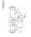
このような双方向DC−DCコンバータは、簡単には降圧動作と昇圧動作を行うDC−DCコンバータをペアで用いれば実現できるが、回路構成が2倍になるため複雑化してしまう。そこで、降圧動作と昇圧動作で共通な回路構成を単一とし、降圧動作時、および昇圧動作時に対し回路構成が異なる部分についてそれぞれスイッチを切り替える双方向DC−DCコンバータが特許文献1に示されている。図6はこのような従来の双方向DC−DCコンバータのブロック回路図である。なお、特許文献1は定電圧出力制御、または定電流出力制御のいずれに対しても、降圧動作、および昇圧動作ができる例を示しているが、そのうち図6では定電圧出力制御を行う場合に必要な回路構成についてのみ抽出して説明する。
Such a bidirectional DC-DC converter can be realized simply by using a pair of DC-DC converters that perform a step-down operation and a step-up operation, but it becomes complicated because the circuit configuration is doubled. Therefore,
図6において、双方向DC−DCコンバータ1は高電圧側蓄電素子2と低電圧側蓄電素子3の間に接続されている。これにより、高電圧側蓄電素子2と低電圧側蓄電素子3のいずれか一方の電力を他方に双方向に充電することができる。
In FIG. 6, the bidirectional DC-
高電圧側蓄電素子2の正極に接続された高電圧側正極端子4には第1スイッチング手段5が接続されている。また、第1スイッチング手段5にはインダクタ6が直列に接続されている。インダクタ6の他端には低電圧側正極端子7を介して低電圧側蓄電素子3の正極が接続されている。
The first switching means 5 is connected to the high voltage side positive terminal 4 connected to the positive electrode of the high voltage
第1スイッチング手段5とインダクタ6の接続点と、高電圧側蓄電素子2の負極に接続された高電圧側負極端子8および低電圧側蓄電素子3の負極に接続された低電圧側負極端子9の接続点の間には、両蓄電素子に対し並列になるように第2スイッチング手段10が接続されている。
A connection point between the first switching means 5 and the
高電圧側正極端子4と高電圧側負極端子8の間には、高電圧側蓄電素子2の電圧を検出して高電圧側制御電圧11を出力する高電圧検出回路12、および高電圧側正極端子4への出力電圧を平滑化する高電圧側コンデンサ13がそれぞれ並列に接続されている。なお、高電圧検出回路12は2つの抵抗12a、12bを直列に接続し、中点電圧を出力する構成としている。
Between the high-voltage-side positive terminal 4 and the high-voltage-side negative terminal 8, a high-
低電圧側正極端子7と低電圧側負極端子9の間にも、高電圧側と同様に低電圧側蓄電素子3の電圧を検出して低電圧側制御電圧14を出力する低電圧検出回路15、および低電圧側コンデンサ16がそれぞれ並列に接続されている。なお、低電圧検出回路15の構成は高電圧検出回路12と同様に2つの抵抗15a、15bの直列接続とした。
A low
高電圧側制御電圧11、および低電圧側制御電圧14は制御電圧切替回路17に接続される。制御電圧切替回路17は2つの入力の内いずれか一方を出力する2入力1出力型3端子スイッチと等価であり、その出力端子は電圧誤差増幅回路18に接続されている。また、制御電圧切替回路17の切替信号19aは切替回路20から得ている。なお、切替回路20は図示しない外部制御回路からの信号に応じて切替信号19aを生成、出力する構成としている。
The high voltage
電圧誤差増幅回路18の出力はPWM比較回路21に入力され、第1スイッチング手段5、および第2スイッチング手段10のオンオフ駆動を行うパルス信号を出力する。パルス信号は電圧の変換方向切替回路22により反転回路23を通すか否かが選択された後、制御信号24として制御回路25に入力される。なお、変換方向切替回路22は1つの入力を2つの出力のいずれかに切り替える1入力2出力型3端子スイッチと等価であり、制御電圧切替回路17と同様に切替回路20からの切替信号19aにより切替制御されている。
The output of the voltage
制御回路25は入力された制御信号24に基づいて第1スイッチング手段5と第2スイッチング手段10を互いに反転動作させるもので、詳しくは、一方は制御信号24をそのまま第1ドライブ回路26に入力し、他方は制御信号24をPWM反転回路27で反転させて第2ドライブ回路28に入力することで互いの反転動作を実現している。なお、第1ドライブ回路26と第2ドライブ回路28への制御信号24の入力は、各々動作スイッチ29によってオンオフされる。動作スイッチ29の制御は切替回路20からの動作信号19bにより行われる。ここで、第1ドライブ回路26と第2ドライブ回路28は制御信号24が動作スイッチ29によってオフにされると、それぞれ第1スイッチング手段5、および第2スイッチング手段10をオフにする回路構成としてある。
The
次に、従来の双方向DC−DCコンバータ1の動作を説明するにあたって、図6に示したブロック回路図に記載される電圧誤差増幅回路18とPWM比較回路21を図7により詳細に説明する。
Next, in describing the operation of the conventional bidirectional DC-
まず、電圧誤差増幅回路18は制御電圧切替回路17で選択された高電圧側制御電圧11、または低電圧側制御電圧14のいずれかがオペアンプ18aの反転入力側に入力される。一方、オペアンプ18aの非反転入力側には高電圧側、または低電圧側の設定電圧が入力される。ここで、設定電圧は降圧動作と昇圧動作で異なるので、高電圧側設定電圧18bと低電圧側設定電圧18cを設定電圧切替回路18dで選択している。従って、設定電圧切替回路18dも切替回路20の切替信号19aにより制御される2入力1出力型3端子スイッチと等価である。これらの構成から、電圧誤差増幅回路18は制御電圧と設定電圧との差を増幅出力している。
First, in the voltage
次に、PWM比較回路21は電圧誤差増幅回路18の出力をオペアンプ21aの非反転入力側に入力するとともに、発振回路21bで生成される基準三角波電圧をオペアンプ21aの反転入力側に入力する。これにより、両者を比較することで電圧誤差増幅回路18の出力に応じたオンオフ比のパルス信号が生成される。
Next, the
次に、従来の双方向DC−DCコンバータの動作について説明する。 Next, the operation of the conventional bidirectional DC-DC converter will be described.
まず、高電圧側から低電圧側への降圧動作について述べる。切替回路20からの切替信号19aにより、降圧動作時の3端子構成の各スイッチは実線に示す方向に切り替えられる。また、動作信号19bにより動作スイッチ29はオンになる。この状態で、低電圧検出回路15の出力である低電圧側制御電圧14が制御電圧切替回路17を介して電圧誤差増幅回路18に入力される。
First, the step-down operation from the high voltage side to the low voltage side will be described. By the
電圧誤差増幅回路18は低電圧側制御電圧14と低電圧側設定電圧18cの差を増幅して出力する。この出力はPWM比較回路21に入力され、前記差に応じたパルス信号を出力する。ここで、変換方向切替回路22は反転回路23側に切り替えられていないため、パルス信号はそのまま制御信号24として制御回路25に入力される。
The voltage
制御回路25では第1ドライブ回路26には制御信号24がそのまま入力され、第2ドライブ回路28にはPWM反転回路27で制御信号25を反転して入力される。これにより、第1スイッチング手段5と第2スイッチング手段10は互いにオンオフ動作が反転される。この結果、高電圧側蓄電素子2の電圧を降圧して低電圧側蓄電素子3を充電する。その際の低電圧側蓄電素子3の電圧は低電圧検出回路15で検出され、電圧誤差増幅回路18に入力される以降の動作が繰り返されるので、低電圧側蓄電素子3の電圧が低電圧側設定電圧18cと等しくなるようにフィードバック制御がなされることになり、定電圧の降圧動作が可能となる。
In the
次に、低電圧側から高電圧側への昇圧動作について述べる。切替回路20からの切替信号19aにより、昇圧動作時の3端子構成の各スイッチは点線に示す方向に切り替えられる。また、動作信号19bにより動作スイッチ29はオンになる。この状態で、高電圧検出回路12の出力である高電圧側制御電圧11が制御電圧切替回路17を介して電圧誤差増幅回路18に入力される。
Next, a boosting operation from the low voltage side to the high voltage side will be described. By the
電圧誤差増幅回路18は高電圧側制御電圧11と高電圧側設定電圧18bの差を増幅して出力する。この出力はPWM比較回路21に入力され、前記差に応じたパルス信号を出力する。ここで、変換方向切替回路22は反転回路23側に切り替えられているので、パルス信号は反転されて制御信号24として制御回路25に入力される。このようにパルス信号を反転させることにより、第1スイッチング手段5と第2スイッチング手段10の動作が降圧時と逆になるため、昇圧することができる。
The voltage
制御回路25では降圧時と同様に第1スイッチング手段5と第2スイッチング手段10が互いに反転したオンオフ動作を行う。この結果、低電圧側蓄電素子3の電圧を昇圧して高電圧側蓄電素子2を充電する。その際の高電圧側蓄電素子2の電圧は高電圧検出回路12で検出され、電圧誤差増幅回路18に入力される以降の動作が繰り返されるので、降圧時と同様にフィードバック制御がなされ、定電圧の昇圧動作が可能となる。
In the
なお、双方向DC−DCコンバータを動作させる必要がないときには切替回路20からの動作信号19bにより動作スイッチ29をオフにする。これにより、第1スイッチング手段5と第2スイッチング手段10がオフになるので、昇降圧動作のいずれもが停止する。
When there is no need to operate the bidirectional DC-DC converter, the
以上の動作により、降圧、または昇圧を切り替えて双方向に電圧変換が可能なDC−DCコンバータを実現していた。
このような従来の双方向DC−DCコンバータは降圧動作時や昇圧動作時に電圧誤差増幅回路18やPWM比較回路21を共用することができるので、確かに回路構成の簡略化が図れる。しかし、そのためには降圧動作、および昇圧動作の切替時に制御電圧切替回路17、設定電圧切替回路18d、および変換方向切替回路22を同時に切り替えなければならず、外部制御可能な3端子スイッチが多数必要な構成であった。
Since such a conventional bidirectional DC-DC converter can share the voltage
ここで、外部制御可能な3端子スイッチとしては信頼性の観点から半導体(例えばFET)を組み合わせた構成が一般的である。この場合の3端子スイッチの回路構成例を図8に示す。この3端子スイッチ30は2入力1出力型3端子スイッチ(図7の制御電圧切替回路17、設定電圧切替回路18d)、および1入力2出力型3端子スイッチ(図7の変換方向切替回路22)の両方に適用することができる。
Here, as a three-terminal switch which can be controlled externally, a configuration in which semiconductors (for example, FETs) are combined is generally used from the viewpoint of reliability. A circuit configuration example of the three-terminal switch in this case is shown in FIG. The three-
図8に示した3端子スイッチ30は、2個のFET32を直列に接続したものを2組用いて、切替信号19aの出力に応じ各組のFET32のオンオフを逆転させることにより、一方の配線経路をオンに、他方をオフにする構成としている。ここで、FET32は点線で示すボディーダイオード35が形成されているので、出力から入力への電流の逆流防止用に、互いに逆向きのFET32を直列に接続している。
The three-
以上のことから、3端子スイッチに相当する実際の回路構成ではFET32が合計4個、およびスイッチ用反転回路37が1個必要となる。この3端子スイッチを3個使用する従来の構成では、降圧動作と昇圧動作を行うDC−DCコンバータをペアで用いるよりは簡素化できるものの、全体の回路構成としては依然複雑さが残るという課題があった。
From the above, an actual circuit configuration corresponding to a three-terminal switch requires a total of four
本発明は、前記従来の課題を解決するもので、簡易な回路構成の双方向DC−DCコンバータを提供することを目的とする。 The present invention solves the above-described conventional problems, and an object thereof is to provide a bidirectional DC-DC converter having a simple circuit configuration.
前記従来の課題を解決するために、本発明の双方向DC−DCコンバータは、定電圧出力制御の場合、高電圧検出回路、および低電圧検出回路の出力をそれぞれ独立して設けた高電圧側誤差増幅回路と低電圧側誤差増幅回路に入力するとともに、互いの極性が反転する構成とし、前記高電圧側誤差増幅回路の出力、または前記低電圧側誤差増幅回路の出力を変換方向切替回路で選択し、その出力を昇降圧動作に対して共通のPWM比較回路から制御回路に入力することで第1スイッチング手段と第2スイッチング手段を駆動する構成とした。これにより、従来の反転回路23、制御電圧切替回路17、および設定電圧切替回路18dを省略できる。
In order to solve the above-described conventional problems, the bidirectional DC-DC converter of the present invention has a high voltage side in which the outputs of the high voltage detection circuit and the low voltage detection circuit are independently provided in the case of constant voltage output control. In addition to being input to the error amplifier circuit and the low voltage side error amplifier circuit, the polarities of each other are reversed, and the output of the high voltage side error amplifier circuit or the output of the low voltage side error amplifier circuit is converted by the conversion direction switching circuit. The first switching means and the second switching means are driven by selecting and inputting the output from the common PWM comparison circuit to the control circuit for the step-up / step-down operation. Thereby, the
また、本発明の双方向DC−DCコンバータは、定電流出力制御の場合、前記定電圧出力制御の構成に対し、高電圧検出回路を、高電圧側蓄電素子への電流を検出して高電圧側制御電圧を出力する高電圧側電流検出回路に置き換えるとともに、低電圧検出回路を、低電圧側蓄電素子への電流を検出して低電圧側制御電圧を出力する低電圧側電流検出回路に置き換えた構成とした。これによっても、従来の反転回路23、制御電圧切替回路17、および設定電圧切替回路18dを省略できる。
In addition, in the case of constant current output control, the bidirectional DC-DC converter of the present invention uses a high voltage detection circuit to detect a current to the high voltage side storage element and detect a high voltage for the constant voltage output control configuration. In addition to replacing the high-voltage side current detection circuit that outputs the low-side control voltage, the low-voltage side detection circuit replaces the low-voltage side current detection circuit that detects the current to the low-voltage side storage element and outputs the low-voltage side control voltage. The configuration was as follows. Also by this, the
また、本発明の双方向DC−DCコンバータは、定電圧出力制御、および定電流出力制御を両方行う場合、高電圧検出回路の出力である第1高電圧側制御電圧、高電圧側電流検出回路の出力である第2高電圧側制御電圧、低電圧検出回路の出力である第1低電圧側制御電圧、および低電圧側電流検出回路の出力である第2低電圧側制御電圧をそれぞれ独立して設けた第1高電圧側誤差増幅回路(第1高電圧側設定電圧の前記第1高電圧側制御電圧に対する差を増幅出力する)、第2高電圧側誤差増幅回路(第2高電圧側設定電圧の前記第2高電圧側制御電圧に対する差を増幅出力する)、第1低電圧側誤差増幅回路(第1低電圧側設定電圧の前記第1低電圧側制御電圧に対する差を増幅し、前記第1高電圧側誤差増幅回路の出力に対し極性を反転して出力する)、および第2低電圧側誤差増幅回路(第2低電圧側設定電圧の前記第2低電圧側制御電圧に対する差を増幅し、前記第2高電圧側誤差増幅回路の出力に対し極性を反転して出力する)に入力し、前記第1高電圧側誤差増幅回路と前記第2高電圧側誤差増幅回路の出力のうち大きい方を高電圧側選択回路で出力するとともに、前記第1低電圧側誤差増幅回路と前記第2低電圧側誤差増幅回路の出力のうち小さい方を低電圧側選択回路で出力し、前記高電圧側選択回路の出力、または前記低電圧側選択回路の出力を変換方向切替回路で選択し、その出力を昇降圧動作に対して共通のPWM比較回路から制御回路に入力することで第1スイッチング手段と第2スイッチング手段を駆動する構成とした。これによっても、従来の反転回路23、制御電圧切替回路17、および設定電圧切替回路18dを省略できる。
Further, the bidirectional DC-DC converter of the present invention, when performing both constant voltage output control and constant current output control, the first high voltage side control voltage and the high voltage side current detection circuit which are the outputs of the high voltage detection circuit. The second high-voltage side control voltage that is the output of the low-voltage detection circuit, the first low-voltage-side control voltage that is the output of the low-voltage detection circuit, and the second low-voltage-side control voltage that is the output of the low-voltage side current detection circuit are independent of each other. A first high voltage side error amplifier circuit (amplifies and outputs a difference of the first high voltage side set voltage with respect to the first high voltage side control voltage), a second high voltage side error amplifier circuit (second high voltage side) Amplifying and outputting the difference of the set voltage with respect to the second high voltage side control voltage), a first low voltage side error amplifier circuit (amplifying the difference of the first low voltage side set voltage with respect to the first low voltage side control voltage; Polarity with respect to the output of the first high voltage side error amplifier circuit And a second low voltage side error amplifier circuit (amplifies the difference of the second low voltage side set voltage with respect to the second low voltage side control voltage), and outputs the second high voltage side error amplifier circuit And output the larger one of the outputs of the first high voltage side error amplifier circuit and the second high voltage side error amplifier circuit by the high voltage side selection circuit, The smaller one of the outputs of the first low voltage side error amplification circuit and the second low voltage side error amplification circuit is output by the low voltage side selection circuit, the output of the high voltage side selection circuit, or the low voltage side selection The first switching means and the second switching means are driven by selecting the output of the circuit by the conversion direction switching circuit and inputting the output from the common PWM comparison circuit to the control circuit for the step-up / step-down operation. Also by this, the
なお、前記構成において、第1高電圧側誤差増幅回路は、第1高電圧側制御電圧の第1高電圧側設定電圧に対する差を増幅出力する構成とし、第2高電圧側誤差増幅回路は、第2高電圧側制御電圧の第2高電圧側設定電圧に対する差を増幅出力する構成とし、高電圧側選択回路は、前記第1高電圧側誤差増幅回路の出力と前記第2高電圧側誤差増幅回路の出力のうち小さい方を出力する構成とするとともに、第1低電圧側誤差増幅回路は、第1低電圧側制御電圧の第1低電圧側設定電圧に対する差を増幅し、その極性を前記第1高電圧側誤差増幅回路の出力に対し反転して出力する構成とし、第2低電圧側誤差増幅回路は、第2低電圧側制御電圧の第2低電圧側設定電圧に対する差を増幅し、その極性を前記第2高電圧側誤差増幅回路の出力に対し反転して出力する構成とし、低電圧側選択回路は前記第1低電圧側誤差増幅回路の出力と前記第2低電圧側誤差増幅回路の出力のうち大きい方を出力する構成としてもよい。これによっても、従来の反転回路23、制御電圧切替回路17、および設定電圧切替回路18dを省略できる。
In the above configuration, the first high voltage side error amplification circuit is configured to amplify and output the difference between the first high voltage side control voltage and the first high voltage side set voltage, and the second high voltage side error amplification circuit is A difference between the second high voltage side control voltage and the second high voltage side set voltage is amplified and output, and the high voltage side selection circuit is configured to output the second high voltage side error and the output of the first high voltage side error amplification circuit. The first low voltage side error amplifying circuit amplifies the difference between the first low voltage side control voltage and the first low voltage side set voltage, and outputs the polarity thereof. The second low voltage side error amplifying circuit amplifies the difference between the second low voltage side control voltage and the second low voltage side set voltage. The polarity of the output of the second high voltage side error amplifier circuit. Against inversion and configured to output, low-voltage-side selection circuit may output a larger one of outputs of said second low-voltage side error amplifier circuit of the first low-voltage side error amplifier circuit. Also by this, the
また、本発明の双方向DC−DCコンバータは、定電圧出力制御、および定電流出力制御を両方行う他の構成の場合、高電圧検出回路の出力である第1高電圧側制御電圧、高電圧側電流検出回路の出力である第2高電圧側制御電圧、低電圧検出回路の出力である第1低電圧側制御電圧、および低電圧側電流検出回路の出力である第2低電圧側制御電圧をそれぞれ独立して設けた第1高電圧側誤差増幅回路(第1高電圧側設定電圧の前記第1高電圧側制御電圧に対する差を増幅出力する)、第2高電圧側誤差増幅回路(第2高電圧側設定電圧の前記第2高電圧側制御電圧に対する差を増幅出力する)、第1低電圧側誤差増幅回路(第1低電圧側設定電圧の前記第1低電圧側制御電圧に対する差を増幅し、前記第1高電圧側誤差増幅回路の出力に対し極性を反転して出力する)、第2低電圧側誤差増幅回路(第2低電圧側設定電圧の前記第2低電圧側制御電圧に対する差を増幅し、前記第2高電圧側誤差増幅回路の出力に対し極性を反転して出力する)に入力し、前記高電圧側誤差増幅回路の出力、または前記低電圧側誤差増幅回路の出力を変換方向切替回路で選択し、前記第2高電圧側誤差増幅回路の出力が最大の時は前記第2高電圧側誤差増幅回路の出力を、前記第2低電圧側誤差増幅回路の出力が最小の時は前記第2低電圧側誤差増幅回路の出力を、それ以外の時は前記変換方向切替回路の出力を、それぞれ制御電圧選択回路で選択し、その出力を昇降圧動作に対して共通のPWM比較回路から制御回路に入力することで第1スイッチング手段と第2スイッチング手段を駆動する構成とした。これによっても、従来の反転回路23、制御電圧切替回路17、および設定電圧切替回路18dを省略できる。
In addition, the bidirectional DC-DC converter of the present invention has the first high-voltage side control voltage, the high voltage, which is the output of the high-voltage detection circuit, in the case of other configurations that perform both constant voltage output control and constant current output control. The second high voltage side control voltage that is the output of the low current side detection circuit, the first low voltage side control voltage that is the output of the low voltage detection circuit, and the second low voltage side control voltage that is the output of the low voltage side current detection circuit Are independently provided, a first high voltage side error amplifier circuit (amplifies and outputs the difference between the first high voltage side set voltage and the first high voltage side control voltage), a second high voltage side error amplifier circuit (first 2) amplifies and outputs the difference between the high voltage side set voltage and the second high voltage side control voltage; and a first low voltage side error amplifier circuit (difference between the first low voltage side set voltage and the first low voltage side control voltage). To the output of the first high-voltage side error amplifier circuit The second low voltage side error amplification circuit (amplifies the difference between the second low voltage side set voltage and the second low voltage side control voltage, and outputs the second low voltage side error amplification circuit) The output of the high voltage side error amplifier circuit or the output of the low voltage side error amplifier circuit is selected by the conversion direction switching circuit, and the second high voltage is output. When the output of the side error amplifier circuit is maximum, the output of the second high voltage side error amplifier circuit is when the output of the second low voltage side error amplifier circuit is minimum. In other cases, the output of the conversion direction switching circuit is selected by the control voltage selection circuit in other cases, and the output is input to the control circuit from the common PWM comparison circuit for the step-up / step-down operation. Driving the switching means and the second switching means It was formed. Also by this, the
なお、前記構成において、第1高電圧側誤差増幅回路は、第1高電圧側制御電圧の第1高電圧側設定電圧に対する差を増幅出力する構成とし、第2高電圧側誤差増幅回路は、第2高電圧側制御電圧の第2高電圧側設定電圧に対する差を増幅出力する構成とし、第1低電圧側誤差増幅回路は、第1低電圧側制御電圧の第1低電圧側設定電圧に対する差を増幅し、その極性を前記第1高電圧側誤差増幅回路の出力に対し反転して出力する構成とし、第2低電圧側誤差増幅回路は、第2低電圧側制御電圧の第2低電圧側設定電圧に対する差を増幅し、その極性を前記第2高電圧側誤差増幅回路の出力に対し反転して出力する構成とするとともに、制御電圧選択回路は、前記第2高電圧側誤差増幅回路の出力が最小の時は前記第2高電圧側誤差増幅回路の出力を、前記第2低電圧側誤差増幅回路の出力が最大の時は前記第2低電圧側誤差増幅回路の出力を、それ以外の時は変換方向切替回路の出力を、それぞれ選択する構成としてもよい。これによっても、従来の反転回路23、制御電圧切替回路17、および設定電圧切替回路18dを省略できる。
In the above configuration, the first high voltage side error amplification circuit is configured to amplify and output the difference between the first high voltage side control voltage and the first high voltage side set voltage, and the second high voltage side error amplification circuit is The difference between the second high-voltage side control voltage and the second high-voltage side set voltage is amplified and output, and the first low-voltage side error amplifying circuit is configured to output the first low-voltage side control voltage to the first low-voltage side set voltage. The difference is amplified and the polarity is inverted and output with respect to the output of the first high voltage side error amplifier circuit. The second low voltage side error amplifier circuit is a second low voltage side control voltage having a second low voltage. The difference with respect to the voltage side set voltage is amplified, the polarity is inverted with respect to the output of the second high voltage side error amplifier circuit, and the control voltage selection circuit is configured to output the second high voltage side error amplifier. When the output of the circuit is minimum, the second high voltage side error amplification circuit The output of the second low voltage side error amplifier circuit is selected when the output of the second low voltage side error amplifier circuit is maximum, and the output of the conversion direction switching circuit is selected otherwise. It is good. Also by this, the
本発明の双方向DC−DCコンバータによれば、電圧誤差増幅回路が増えるものの、それより回路構成が複雑な3端子スイッチを従来の3個から1個に減らすことができ、さらに反転回路も不要となるので、全体として簡易な回路構成の双方向DC−DCコンバータを実現することができる。 According to the bidirectional DC-DC converter of the present invention, although the voltage error amplifier circuit is increased, the number of three-terminal switches having a complicated circuit configuration can be reduced from the conventional three to one, and an inverting circuit is not required. Therefore, a bidirectional DC-DC converter having a simple circuit configuration as a whole can be realized.
以下、本発明を実施するための最良の形態について、図面を参照しながら説明する。 The best mode for carrying out the present invention will be described below with reference to the drawings.
(実施の形態1)
図1は、本発明の実施の形態1における双方向DC−DCコンバータのブロック回路図である。図2は、本発明の実施の形態1における双方向DC−DCコンバータの一部詳細ブロック回路図である。図1、および図2において従来の図6、および図7と同じ構成要素については同じ符号を用い、詳細な説明を省略する。また、本実施の形態1では定電圧出力制御を行う場合について説明する。
(Embodiment 1)
FIG. 1 is a block circuit diagram of a bidirectional DC-DC converter according to
まず図1において、図6に示した従来例との回路構成上の相違点を以下に示す。 First, in FIG. 1, differences in circuit configuration from the conventional example shown in FIG. 6 are shown below.
1)高電圧側蓄電素子2の電圧を検出する高電圧検出回路12の出力(高電圧側制御電圧11)は高電圧側誤差増幅回路50に、低電圧側蓄電素子3の電圧を検出する低電圧検出回路15の出力(低電圧側制御電圧14)は低電圧側誤差増幅回路51に、それぞれ独立して入力される構成とした。
1) The output (high voltage side control voltage 11) of the high
2)それに伴って制御電圧切替回路17を廃した。
2) Along with this, the control
3)高電圧側誤差増幅回路50の出力と低電圧側誤差増幅回路51の出力の極性が互いに反転する構成とした。なお、本実施の形態1では高電圧側誤差増幅回路50の出力に対し低電圧側誤差増幅回路51の出力の極性が反転するように、図2に示すオペアンプ18aの非反転入力と反転入力を互いに逆に接続する構成としている。
3) The polarities of the output of the high voltage side
4)それに伴って、反転回路23を廃した。
4) Along with this, the
5)高電圧側誤差増幅回路50の出力と低電圧側誤差増幅回路51の出力を図8の3端子スイッチ30で構成される変換方向切替回路22の入力端子にそれぞれ接続した。
5) The output of the high voltage side
6)変換方向切替回路22の出力を共通のPWM比較回路21に接続した。
6) The output of the conversion
7)PWM比較回路21の出力を共通の制御回路25に接続した。
7) The output of the
以上の相違点から図1と図6の回路構成を比較すると、本実施の形態1では電圧誤差増幅回路18が高電圧側誤差増幅回路50と低電圧側誤差増幅回路51に分かれるとともに、制御電圧切替回路17が無い構成となることがわかる。また、反転回路23も無い構成となる。なお、PWM比較回路21と制御回路25は従来と同様に共通とした構成である。
Comparing the circuit configurations of FIG. 1 and FIG. 6 from the above differences, in the first embodiment, the voltage
次に、さらに詳細に両者の相違点を図2、および図7の対比から以下に示す。 Next, the difference between the two will be described in more detail below from the comparison of FIG. 2 and FIG.
8)高電圧側設定電圧18bを高電圧側誤差増幅回路50に、低電圧側設定電圧18cを低電圧側誤差増幅回路51に、それぞれ内蔵した。
8) The high voltage side set
9)それに伴い、設定電圧切替回路18dを廃した。
9) Accordingly, the set
以上の相違点から図2と図7の回路構成を比較すると、本実施の形態1では高電圧側誤差増幅回路50と低電圧側誤差増幅回路51にそれぞれオペアンプ18aが必要となるため、オペアンプ18aが1個増加しているものの、制御電圧切替回路18dが無い構成となることがわかる。
Comparing the circuit configurations of FIG. 2 and FIG. 7 from the above differences, the first embodiment requires the
従って、図1、図2より従来との回路構成上の相違点をまとめると、本実施の形態1はオペアンプ18aが1個増え、制御電圧切替回路17、および制御電圧切替回路18dの2個の3端子スイッチ30が無く、反転回路23も不要である以外は、従来と同じであることがわかる。ここで、外部制御可能な3端子スイッチ30の回路構成は図8で説明した通り多くの部品を使用する複雑な構成であり、一方、オペアンプ18aについては、例えば1パッケージに4個のオペアンプが内蔵されたICが容易に入手可能であることから、オペアンプ18aが1個増えても回路構成がそれほど複雑になることはない。
Therefore, the differences in the circuit configuration from the prior art are summarized from FIG. 1 and FIG. 2, in the first embodiment, the
以上のことから、全体的には本実施の形態1の回路構成の方が従来の多数の3端子スイッチ30や反転回路23を使用する構成より簡易であることがわかる。
From the above, it can be seen that the overall circuit configuration of the first embodiment is simpler than the configuration using many conventional three-
次に、本実施の形態1の双方向DC−DCコンバータ1の動作について説明する。
Next, the operation of the bidirectional DC-
まず、高電圧側から低電圧側への降圧動作について述べる。切替回路20から生成された切替信号19aにより、降圧動作時の変換方向切替回路22は実線に示す方向に切り替えられる。また、動作信号19bにより動作スイッチ29はオンになる。この状態で、高電圧検出回路12の出力である高電圧側制御電圧11が高電圧側誤差増幅回路50に、低電圧検出回路15の出力である低電圧側制御電圧14が低電圧側誤差増幅回路51に、それぞれ入力される。この際、図2に示すようにオペアンプ18aへの接続は非反転入力と反転入力が高電圧側誤差増幅回路50と低電圧側誤差増幅回路51で互いに逆になるようにしている。これにより、両者の出力は極性が互いに反転することになる。
First, the step-down operation from the high voltage side to the low voltage side will be described. By the
入力された各電圧はそれぞれ高電圧側設定電圧18b、および低電圧側設定電圧18cとの差を増幅して高電圧側誤差増幅回路50、および低電圧側誤差増幅回路51から互いに反転した状態で出力される。
Each input voltage is in a state in which the difference between the high voltage side set
高電圧側誤差増幅回路50の出力、および低電圧側誤差増幅回路51の出力は変換方向切替回路22に入力されるが、降圧動作の場合は後者の出力が選択される。これにより、低電圧側の出力電圧を一定に制御できる。
The output of the high voltage side
変換方向切替回路22の出力はPWM比較回路21に入力され、前記差に応じたパルス信号、すなわち制御信号24を出力する。この動作の詳細は従来と同様である。制御信号24は制御回路25に入力される。
The output of the conversion
制御回路25の動作は従来と同じであるので説明を省略するが、これにより第1スイッチング手段5と第2スイッチング手段10は互いにオンオフが反転する動作を行う。なお、第1スイッチング手段5と第2スイッチング手段10にはFETを用いた。この結果、高電圧側蓄電素子2の電圧を降圧して低電圧側蓄電素子3を充電する。その際の低電圧側蓄電素子3の電圧が低電圧検出回路15で検出され、低電圧側誤差増幅回路51に入力される以降の動作が繰り返されるので、低電圧側蓄電素子3の電圧が低電圧側設定電圧18cと等しくなるようにフィードバック制御がなされることになり、定電圧の降圧動作が可能となる。
Since the operation of the
次に、低電圧側から高電圧側への昇圧動作について述べる。切替回路20からの切替信号19aにより、昇圧動作時の変換方向切替回路22は点線に示す方向に切り替えられる。また、動作信号19bにより動作スイッチ29はオンになる。この状態で、降圧動作時と同様に高電圧側制御電圧11が高電圧側誤差増幅回路50に、低電圧側制御電圧14が低電圧側誤差増幅回路51に、それぞれ入力される。
Next, a boosting operation from the low voltage side to the high voltage side will be described. By the
入力された各電圧はそれぞれ高電圧側設定電圧18b、および低電圧側設定電圧18cとの差を増幅して高電圧側誤差増幅回路50、および低電圧側誤差増幅回路51から互いに極性が反転した状態で出力される。
Each input voltage amplifies the difference between the high voltage side set
高電圧側誤差増幅回路50の出力、および低電圧側誤差増幅回路51の出力は変換方向切替回路22に入力されるが、昇圧動作の場合は前者の出力が選択される。これにより、高電圧側の出力電圧を一定に制御できる。
The output of the high voltage side
変換方向切替回路22の出力はPWM比較回路21に入力され、前記差に応じた制御信号24を出力する。制御信号24は制御回路25に入力される。
The output of the conversion
制御回路25の動作は従来と同じであるので説明を省略するが、これにより第1スイッチング手段5と第2スイッチング手段10は互いにオンオフが反転する動作を行う。この際、高電圧側誤差増幅回路50の出力が低電圧側誤差増幅回路51の出力に対し極性が反転しているため、制御信号24は降圧動作と逆の出力となる。これにより、低電圧側蓄電素子3の電圧を昇圧して高電圧側蓄電素子2を充電する。その際の高電圧側蓄電素子2の電圧が高電圧検出回路12で検出され、高電圧側誤差増幅回路50に入力される以降の動作が繰り返されるので、高電圧側蓄電素子2の電圧が高電圧側設定電圧18bと等しくなるようにフィードバック制御がなされることになり、定電圧の昇圧動作が可能となる。
Since the operation of the
なお、双方向DC−DCコンバータを動作させる必要がないときには従来と同様に切替回路20からの動作信号19bにより動作スイッチ29をオフにする。これにより、第1スイッチング手段5と第2スイッチング手段10がオフになるので、昇降圧動作のいずれもが停止する。
When there is no need to operate the bidirectional DC-DC converter, the
このような動作から、本実施の形態1の回路構成でも従来と全く同様の降圧動作、および昇圧動作が可能であることがわかる。 From such an operation, it can be seen that the same step-down operation and step-up operation as in the prior art are possible even in the circuit configuration of the first embodiment.
以上の構成、動作により、降圧、または昇圧を切り替えて双方向に定電圧出力制御が可能な簡易双方向DC−DCコンバータが実現できた。 With the above configuration and operation, a simple bidirectional DC-DC converter capable of bidirectionally controlling constant voltage output by switching between step-down and step-up can be realized.
(実施の形態2)
図3は、本発明の実施の形態2における双方向DC−DCコンバータの一部詳細ブロック回路図である。図3において図2と同じ構成要素については同じ符号を用い、詳細な説明を省略する。また、本実施の形態2では定電流出力制御を行う場合について説明する。
(Embodiment 2)
FIG. 3 is a partial detailed block circuit diagram of the bidirectional DC-DC converter according to
まず、図3において図2との回路構成上の相違点を以下に示す。 First, differences in the circuit configuration of FIG. 3 from FIG. 2 will be described below.
1)定電流出力制御とするため、高電圧側電流検出回路52、および低電圧側電流検出回路53を設けた。
1) A high voltage side
2)それに伴い、高電圧検出回路12、および低電圧検出回路15を廃した。
2) Accordingly, the high
上記以外の回路構成は実施の形態1と同じである。従って、定電流出力制御を行う場合についても3端子スイッチ30は変換方向切替回路22のみであり、反転回路23も不要となるので、従来に比べオペアンプ18aが1個増えるものの、全体としての回路構成は簡易化されることがわかる。
The circuit configuration other than the above is the same as that of the first embodiment. Accordingly, even when the constant current output control is performed, the three-
図3の双方向DC−DCコンバータ1の動作は、降圧動作、昇圧動作ともに、実施の形態1で述べた定電圧出力制御に替わって定電流出力制御になる以外は全く同じである。すなわち、降圧動作の場合は、まず低電圧側電流検出回路53から低電圧側蓄電素子3への電流に比例した電圧出力を得る。なお、低電圧側電流検出回路53はホール素子等の電流センサで構成してもよいし、低抵抗をインダクタ6と直列に接続し、その両端電圧から求めてもよい。
The operation of the bidirectional DC-
電流に比例した電圧出力は低電圧側誤差増幅回路51に入力され、そこで低電圧側設定電圧18cとの差を増幅して出力する。それ以降の動作は実施の形態1と同じである。その結果、低電圧側蓄電素子3に流れる電流が低電圧側設定電圧18cで決定される電流値になるようにフィードバック制御される。
The voltage output proportional to the current is input to the low voltage side
また、昇圧動作の場合も高電圧側電流検出回路52で高電圧側蓄電素子2への電流に比例した電圧出力が高電圧側誤差増幅回路50に入力され、そこで高電圧側設定電圧18bとの差を増幅して出力する。この出力は低電圧側誤差増幅回路51の出力と極性が反転しているので、昇圧動作が行われる。この反転した出力は変換方向切替回路22を介してPWM比較回路21に入力される。それ以降の動作は実施の形態1と同じである。その結果、高電圧側蓄電素子2に流れる電流が高電圧側設定電圧18bで決定される電流値になるようにフィードバック制御される。
Also in the step-up operation, the high voltage side
なお、動作スイッチ29の役割と動作も実施の形態1と同じである。
The role and operation of the
このような動作から、本実施の形態2の回路構成でも従来と同様に定電流出力制御による降圧動作、および昇圧動作が可能であることがわかる。 From such an operation, it can be seen that the step-down operation and the step-up operation by the constant current output control can be performed in the circuit configuration of the second embodiment as in the conventional case.
以上の構成、動作により、降圧、または昇圧を切り替えて双方向に定電流出力制御が可能な簡易双方向DC−DCコンバータが実現できた。 With the above configuration and operation, a simple bidirectional DC-DC converter capable of bidirectionally controlling constant current output by switching the step-down or step-up can be realized.
(実施の形態3)
図4は、本発明の実施の形態3における双方向DC−DCコンバータの一部詳細ブロック回路図である。図4において図2、および図3と同じ構成要素については同じ符号を用い、詳細な説明を省略する。また、本実施の形態3では定電圧出力制御、および定電流出力制御を両方行う場合について説明する。
(Embodiment 3)
FIG. 4 is a partial detailed block circuit diagram of the bidirectional DC-DC converter according to
まず、図4において図2との回路構成上の相違点を以下に示す。 First, differences in the circuit configuration of FIG. 4 from FIG. 2 will be described below.
1)高電圧側に高電圧検出回路12、および高電圧側電流検出回路52を両方設け、同様に低電圧側に低電圧検出回路15、および低電圧側電流検出回路53を両方設けた。
1) Both the high
2)それに伴い、それぞれの出力に電圧誤差増幅回路、すなわち順番に第1高電圧側誤差増幅回路54、第2高電圧側誤差増幅回路55、第1低電圧側誤差増幅回路56、および第2低電圧側誤差増幅回路57を接続した。
2) Along with this, a voltage error amplifier circuit is connected to each output, that is, a first high voltage side
3)それぞれの電圧誤差増幅回路に内蔵される設定電圧を順番に第1高電圧側設定電圧18h、第2高電圧側設定電圧18e、第1低電圧側設定電圧18f、および第2低電圧側設定電圧18gとして設けた。
3) The first high voltage side set
4)第1高電圧側誤差増幅回路54の出力は第1高電圧側設定電圧18hの第1高電圧側制御電圧62に対する差の増幅出力とし、第1低電圧側誤差増幅回路56の出力は第1低電圧側制御電圧60の第1低電圧側設定電圧18fに対する差の増幅出力となるように接続することで、極性が互いに反転するようにした。なお、例えば「第1高電圧側設定電圧18hの第1高電圧側制御電圧62に対する差」とは、後者(第1高電圧側制御電圧62)を基準とした時の前者(第1高電圧側設定電圧18h)との差を示すものであり、回路上では図4のオペアンプ18aの反転入力側に入力される電圧を前者(第1高電圧側設定電圧18h)に、非反転入力側に入力される電圧を後者(第1高電圧側制御電圧62)に接続したことを示す。従って、第1高電圧側誤差増幅回路54の出力と第1低電圧側誤差増幅回路56の出力の極性を互いに反転させるために、第1低電圧側誤差増幅回路56においては第1高電圧側誤差増幅回路54とは逆に「第1低電圧側制御電圧60の第1低電圧側設定電圧18fに対する差」を増幅出力している。これは、回路上では図4のオペアンプ18aの反転入力側に第1低電圧側制御電圧60を、非反転入力側に第1低電圧側設定電圧18fを接続する構成となる。この回路構成により、第1低電圧側設定電圧18fの第1低電圧側制御電圧60に対する差を増幅し、その極性を第1高電圧側誤差増幅回路54の出力に対し反転して出力することと等価になる。なお、以下の説明においても前記と同様の記述は同様の意味であると定義する。
4) The output of the first high voltage side
5)第2高電圧側誤差増幅回路55の出力は第2高電圧側設定電圧18eの第2高電圧側制御電圧63に対する差の増幅出力とし、第2低電圧側誤差増幅回路57の出力は第2低電圧側制御電圧61の第2低電圧側設定電圧18gに対する差の増幅出力となるように接続することで、極性が互いに反転するようにした。
5) The output of the second high voltage side
6)第1高電圧側誤差増幅回路54と第2高電圧側誤差増幅回路55の出力のうち大きい方を出力する高電圧側選択回路58、および第1低電圧側誤差増幅回路56と第2低電圧側誤差増幅回路57の出力のうち小さい方を出力する低電圧側選択回路59を設けた。
6) A high voltage
7)高電圧側選択回路58の出力と低電圧側選択回路59の出力を変換方向切替回路22に接続した。
7) The output of the high voltage
以上のように構成することで、反転回路23が不要な上、3端子スイッチ30が変換方向切替回路22のみの簡易な回路構成で、かつ検出された被制御側の電圧、または電流が一定になるように動作できる双方向DC−DCコンバータ1が得られる。
With the configuration as described above, the inverting
次に、本実施の形態3の双方向DC−DCコンバータ1の動作について説明する。なお、ここでは双方向DC−DCコンバータ1を以下に示す自動車に応用した例について説明する。
Next, the operation of the bidirectional DC-
自動車に双方向DC−DCコンバータ1を搭載するシステムとしては、例えば高電圧側蓄電素子2として自動車のバッテリ(定格電圧12V)が、低電圧側蓄電素子3として電気二重層キャパシタを直列や直並列に接続したキャパシタユニット(定格電圧5V)が接続されたものが想定される。ここで、キャパシタユニットの定格電圧をバッテリの定格電圧より下げるのは、キャパシタの必要数が削減でき小型化が可能となるからである。但し、その分、バッテリとキャパシタ間の充電時に双方向DC−DCコンバータが必要となる。
As a system in which the bidirectional DC-
このような構成のシステムは、自動車が制動動作をしている時に発生する発電機(バッテリに並列接続されている)の電力を急速充放電特性に優れるキャパシタユニットに一旦蓄え、非制動時にキャパシタユニットの電力を補機やバッテリに放出することにより制動エネルギーを電気エネルギーとして回生できるので、低燃費化に貢献できる。 The system having such a configuration temporarily stores the electric power of the generator (connected in parallel with the battery) generated when the vehicle is braking in a capacitor unit having excellent rapid charge / discharge characteristics, and the capacitor unit when not braking. Since the braking energy can be regenerated as electric energy by discharging the electric power to the auxiliary equipment and the battery, it can contribute to the reduction in fuel consumption.
ここでは上記システムにおいて、バッテリとキャパシタユニットの相互充電動作について説明する。但し、キャパシタユニットは電気二重層キャパシタを直列、または直並列に接続することにより定格電圧を5Vとした構成について説明するが、電気二重層キャパシタ1個あたりの定格電圧が約2.5Vであるので、定格電圧を2.5Vとして単体で用いる構成としてもよいし、これを複数並列に接続して大容量化した構成としてもよい。 Here, the mutual charging operation of the battery and the capacitor unit in the above system will be described. However, the capacitor unit will be described with a configuration in which the rated voltage is 5 V by connecting the electric double layer capacitors in series or in series-parallel, but the rated voltage per electric double layer capacitor is about 2.5 V. The rated voltage may be set to 2.5 V and used alone, or a plurality of these may be connected in parallel to increase the capacity.
まず、高電圧側蓄電素子2(バッテリや発電機)から低電圧側蓄電素子3(キャパシタユニット)への充電に対する降圧動作について説明する。切替回路20からの切替信号19aにより、降圧動作時の変換方向切替回路22は実線に示す方向に切り替えられる。従って、高電圧検出回路12から第1高電圧側誤差増幅回路54を介して得られる出力と高電圧側電流検出回路52から第2高電圧側誤差増幅回路55を介して得られる出力のうち、大きい方の出力(高電圧側選択回路58により得られる)は、降圧動作には使用されない。また、動作信号19bにより動作スイッチ29はオンになっている。
First, a step-down operation for charging from the high voltage side storage element 2 (battery or generator) to the low voltage side storage element 3 (capacitor unit) will be described. By the
この状態で、低電圧検出回路15の出力電圧である第1低電圧側制御電圧60が第1低電圧側誤差増幅回路56に、低電圧側電流検出回路53の出力電圧である第2低電圧側制御電圧61が第2低電圧側誤差増幅回路57にそれぞれ入力される。第1低電圧側誤差増幅回路56では第1低電圧側制御電圧60の第1低電圧側設定電圧18fに対する差を増幅して出力する。一方、第2低電圧側誤差増幅回路57では第2低電圧側制御電圧61の第2低電圧側設定電圧18gに対する誤差を増幅して出力する。これら2つの出力電圧は低電圧側選択回路59に入力される。低電圧側選択回路59は入力された2つの電圧の比較を行い、電圧の小さい方をそのまま出力する。このように出力することにより、定電圧出力制御、または定電流出力制御のいずれか設定電圧に近い方で降圧制御を行うことになる。
In this state, the first low voltage
その後の動作は実施の形態1、2と同様にPWM比較回路21で制御信号24を生成し、制御回路25に入力することで第1スイッチング手段5と第2スイッチング手段10をフィードバック制御して定電圧出力制御、または定電流出力制御を行う。
The subsequent operation is the same as in the first and second embodiments, in which the
このような制御は、前記自動車のシステムにおいて、例えば車両制動時のようにキャパシタユニット(図示せず)に制動エネルギーを蓄える動作に相当する。この場合、最初にキャパシタユニットには電荷が蓄えられていないので、その両端電圧は0V近傍となる。従って、第1低電圧側制御電圧60は0V近傍である。そこに制動により発電した電力が高電圧側正極端子4を介して双方向DC−DCコンバータ1に入力される。この時、被制御側であるキャパシタユニットの設定電圧(第1低電圧側設定電圧18f)は定格の5Vであるので、第1低電圧側制御電圧60(0V近傍)と比べ後者の前者に対する差、すなわち第1低電圧側設定電圧18fを基準とした時の第1低電圧側制御電圧60との差が極めて大きい状態であることになる。従って、低電圧側選択回路59は低電圧側電流検出回路53の出力である第2低電圧側制御電圧61の第2低電圧側設定電圧18gに対する差を増幅した電圧の方が小さいので、その電圧を選択し、それを基に定電流出力制御を行う。これにより、キャパシタユニットへは、まず定電流で充電される。
Such control corresponds to an operation of storing braking energy in a capacitor unit (not shown) in the automobile system, for example, during vehicle braking. In this case, since no charge is initially stored in the capacitor unit, the voltage between both ends thereof is in the vicinity of 0V. Therefore, the first low voltage
このようにして定電流充電が進むと、キャパシタユニットの両端電圧は上昇し、やがて低電圧検出回路15の出力である第1低電圧側制御電圧60の第1低電圧側設定電圧18fに対する差の方が小さくなる。これにより、低電圧側選択回路59は第1低電圧側制御電圧60の第1低電圧側設定電圧18fに対する差を増幅した電圧を選択し、それを基に定電圧出力制御を行うことになる。その結果、キャパシタユニットへは定電流出力制御のみによる満充電時の電圧オーバーシュートを避けることができ、キャパシタユニットの劣化を抑制した充電が自動的に行える。
When the constant current charging proceeds in this way, the voltage across the capacitor unit increases, and eventually the difference between the first low voltage
次に、低電圧側蓄電素子3(キャパシタユニット)から高電圧側蓄電素子2(バッテリ)への充電に対する昇圧動作について説明する。切替回路20からの切替信号19aにより、昇圧動作時の変換方向切替回路22は点線に示す方向に切り替えられる。従って、低電圧検出回路15から第1低電圧側誤差増幅回路56を介して得られる出力と低電圧側電流検出回路53から第2低電圧側誤差増幅回路57を介して得られる出力のうち、小さい方の出力(低電圧側選択回路59により得られる)は、昇圧動作には使用されない。また、動作信号19bにより動作スイッチ29はオンになっている。
Next, a boosting operation for charging from the low voltage storage element 3 (capacitor unit) to the high voltage storage element 2 (battery) will be described. By the
この状態で、高電圧検出回路12の出力電圧、すなわち第1高電圧側制御電圧62が第1高電圧側誤差増幅回路54に、高電圧側電流検出回路52の出力電圧、すなわち第2高電圧側制御電圧63が第2高電圧側誤差増幅回路55にそれぞれ入力される。第1高電圧側誤差増幅回路54では第1高電圧側設定電圧18hの第1高電圧側制御電圧62に対する差を増幅して出力する。一方、第2高電圧側誤差増幅回路55では第2高電圧側設定電圧18eの第2高電圧側制御電圧63に対する差を増幅して出力する。これら2つの出力電圧は高電圧側選択回路58に入力される。高電圧側選択回路58は入力された2つの電圧の比較を行い、電圧の大きい方を出力する。この出力は前記した降圧動作時の出力とは極性が反転しているので、定電圧出力制御、または定電流出力制御のいずれか設定電圧に近い方で昇圧制御を行うことになる。
In this state, the output voltage of the high
その後の動作は実施の形態1、2と同様にPWM比較回路21で制御信号24を生成し、制御回路25に入力することで第1スイッチング手段5と第2スイッチング手段10をフィードバック制御して定電圧出力制御、または定電流出力制御を行う。
The subsequent operation is the same as in the first and second embodiments, in which the
このような制御は、前記した自動車のシステムにおいて、例えば車両制動によりキャパシタユニットに蓄えられた電力でバッテリ(図示せず)を充電する動作に相当する。この場合、バッテリの両端電圧は通常時であれば定格電圧に近い12V近傍となる。従って、第1高電圧側制御電圧62は12V近傍である。そこにキャパシタユニットの電力が低電圧側正極端子7を介して双方向DC−DCコンバータ1に入力される。この時、被制御側であるバッテリの設定電圧(第1高電圧側設定電圧18h)は定格の12Vであるので、第1高電圧側設定電圧18hの第1高電圧側制御電圧62に対する差、すなわち後者を基準とした前者との差は0近傍となる。一方、第2高電圧側制御電圧63の出力は、電流が流れることにより第2高電圧側設定電圧18eと異なった値となり、後者の前者に対する差は負の値を有することになる。これは、オペアンプ18aへの第2高電圧側制御電圧63と第2高電圧側設定電圧18eの接続が低電圧側におけるオペアンプ18aへの接続と逆転しているためである。従って、高電圧側選択回路58は第1高電圧側設定電圧18hの第1高電圧側制御電圧62に対する差と、第2高電圧側設定電圧18eの第2高電圧側制御電圧63に対する差のうち、電圧の大きい方を選択出力するので、この場合では高電圧側選択回路58は後者の差を出力し、それを基に定電圧出力制御を行う。これにより、バッテリへは定電圧で充電されるので、満充電時の電圧オーバーシュートを避けることができ、バッテリの劣化を抑制した充電が行える。
Such control corresponds to an operation of charging a battery (not shown) with electric power stored in the capacitor unit by vehicle braking, for example, in the above-described automobile system. In this case, the voltage across the battery is in the vicinity of 12V, which is close to the rated voltage, at normal times. Accordingly, the first high voltage
一方、大電力を消費する補機(例えばスターターモーターや電動パワーステアリング等)が使用されているときは、バッテリの両端電圧は定格電圧を相当下回り、数Vオーダーになることがある。従って、第1高電圧側制御電圧62は数V程度である。この場合でも被制御側であるバッテリの設定電圧(第1高電圧側設定電圧18h)は定格の12Vであるので、第1高電圧側設定電圧18hの第1高電圧側制御電圧62に対する差は負の値を持ち、極めて小さくなる。従って、高電圧側選択回路58は第2高電圧側設定電圧18eの第2高電圧側制御電圧63に対する差を増幅した電圧の方が大きいので、その電圧を選択し、それを基に定電流出力制御を行う。これにより、バッテリへは、まず定電流で充電される。
On the other hand, when an auxiliary machine that consumes a large amount of power (for example, a starter motor or an electric power steering) is used, the voltage across the battery may be considerably lower than the rated voltage and may be on the order of several volts. Accordingly, the first high voltage
このようにして定電流充電が進んだり、大電力を消費する補機が停止すると、バッテリの両端電圧は上昇し、やがて第1高電圧側設定電圧18hの第1高電圧側制御電圧62に対する差の方が大きくなる。これにより、高電圧側選択回路58は第1高電圧側設定電圧18hの第1高電圧側制御電圧62に対する差を増幅した電圧を選択し、それを基に定電圧出力制御を行うことになる。その結果、バッテリへは定電流出力制御のみによる満充電時の電圧オーバーシュートを避けることができ、バッテリの劣化を抑制した充電が自動的に行える。
When the constant current charging proceeds in this way or the auxiliary machine that consumes a large amount of power stops, the voltage across the battery rises, and eventually the difference between the first high voltage side set
なお、動作スイッチ29の役割と動作は実施の形態1と同じである。
The role and operation of the
このような動作から、本実施の形態3の回路構成でも従来と同様に定電圧出力制御、または定電流出力制御による降圧動作、および昇圧動作が可能であることがわかる。 From such an operation, it can be seen that the step-down operation and the step-up operation by the constant voltage output control or the constant current output control can be performed in the circuit configuration of the third embodiment as in the prior art.
以上の構成、動作により、降圧、または昇圧を切り替えて双方向に定電圧出力制御、または定電流出力制御が可能な簡易双方向DC−DCコンバータが実現できた。 With the above configuration and operation, a simple bidirectional DC-DC converter capable of bidirectionally performing constant voltage output control or constant current output control by switching step-down or step-up can be realized.
なお、本実施の形態3における4個のオペアンプ18aへの反転入力、および非反転入力を全て逆に接続する構成としてもよい。但し、この場合は高電圧側選択回路58に入力される2種類の電圧の極性が反転するので、高電圧側選択回路58は2つの入力電圧のうち小さい方を出力するとともに、低電圧側選択回路59に入力される2種類の電圧の極性も反転するので、低電圧側選択回路59は2つの入力電圧のうち大きい方を出力する構成とする必要がある。
In addition, it is good also as a structure which reversely connects all the inverting inputs and non-inverting inputs to the four
(実施の形態4)
図5は、本発明の実施の形態4における双方向DC−DCコンバータの一部詳細ブロック回路図である。図5において図4と同じ構成要素については同じ符号を用い、詳細な説明を省略する。また、本実施の形態4でも実施の形態3と同様に定電圧出力制御、および定電流出力制御を両方行う場合について説明する。
(Embodiment 4)
FIG. 5 is a partial detailed block circuit diagram of the bidirectional DC-DC converter according to Embodiment 4 of the present invention. 5, the same components as those in FIG. 4 are denoted by the same reference numerals, and detailed description thereof is omitted. In the fourth embodiment, a case where both constant voltage output control and constant current output control are performed as in the third embodiment will be described.
まず、図5において図4との回路構成上の相違点を以下に示す。 First, differences in the circuit configuration of FIG. 5 from FIG. 4 will be described below.
1)第1高電圧側誤差増幅回路54の出力、および第1低電圧側誤差増幅回路56の出力を変換方向切替回路22に接続した。
1) The output of the first high voltage side
2)第2高電圧側誤差増幅回路55の出力、第2低電圧側誤差増幅回路57の出力、および変換方向切替回路22の出力を制御電圧選択回路64に接続した。
2) The output of the second high voltage side
3)制御電圧選択回路64は第2高電圧側誤差増幅回路55の出力が最大の時はその出力を、第2低電圧側誤差増幅回路57の出力が最小の時はその出力を、それ以外の時は変換方向切替回路22の出力を、それぞれ選択する構成とした。
3) The control
4)制御電圧選択回路64の出力がPWM比較回路21に入力される構成とした。
4) The output of the control
5)以上の構成に伴い、高電圧側選択回路58、および低電圧側選択回路59を廃した。
5) With the above configuration, the high voltage
このように構成することで、反転回路23が不要で、3端子スイッチ30が変換方向切替回路22のみとなり、さらに高電圧側選択回路58、および低電圧側選択回路59を制御電圧選択回路64に統合した簡易な回路構成となり、かつ検出された被制御側の電圧、または電流が一定になるように動作できる双方向DC−DCコンバータ1が得られる。
With this configuration, the inverting
次に、本実施の形態4の双方向DC−DCコンバータ1の動作について実施の形態3と異なる部分を中心に説明する。
Next, the operation of the bidirectional DC-
まず、高電圧側蓄電素子2から低電圧側蓄電素子3への充電に対する降圧動作について説明する。この場合も変換方向切替回路22は実線に示す方向に切り替えられる。従って、高電圧検出回路12から第1高電圧側誤差増幅回路54を介して得られる出力は、降圧動作には使用されない。また、動作信号19bにより動作スイッチ29はオンになっている。
First, a step-down operation for charging from the high voltage
この状態で、低電圧検出回路15の出力電圧である第1低電圧側制御電圧60が第1低電圧側誤差増幅回路56に、高電圧側電流検出回路52の出力電圧である第2高電圧側制御電圧63が第2高電圧側誤差増幅回路55に、低電圧側電流検出回路53の出力電圧である第2低電圧側制御電圧61が第2低電圧側誤差増幅回路57にそれぞれ入力される。これらの入力は順に、第1低電圧側設定電圧18f、第2高電圧側設定電圧18e、および第2低電圧側設定電圧18gとの差を増幅されて出力される。なお、本実施の形態4における差を得る際の基準となる電圧は、高電圧側では制御電圧であり、低電圧側では設定電圧とした。
In this state, the first low voltage
これら3種の出力は全て制御電圧選択回路64に入力される。なお、第1低電圧側誤差増幅回路56の出力は変換方向切替回路22を介して入力される。制御電圧選択回路64は第2高電圧側誤差増幅回路55の出力が最大の時はその出力を、第2低電圧側誤差増幅回路57の出力が最小の時はその出力を、それ以外の時は変換方向切替回路22の出力を、それぞれ選択する構成としている。ここでは降圧動作についての説明であるので、その場合の制御電圧選択回路64の動作について述べる。
All these three types of outputs are input to the control
実施の形態3で述べたように降圧動作の初期では低電圧側蓄電素子3が蓄電されておらず0V近傍である。この場合、低電圧側蓄電素子3を満充電するために、高電圧側蓄電素子2から低電圧側蓄電素子3に電流が流れる。この時の電流値は高電圧側蓄電素子2と低電圧側蓄電素子3の電圧差が最大であるので、大電流が流れようとする。この電流値は低電圧側蓄電素子3への電流値を検出する低電圧側電流検出回路53から第2低電圧側制御電圧61として出力される。この出力は第2低電圧側誤差増幅回路57に入力され、第2低電圧側設定電圧18gに対する差が増幅される。従って、低電圧側蓄電素子3への電流値は直ちに第2低電圧側設定電圧18gを超える。ここで、図5より第2低電圧側誤差増幅回路57のオペアンプ18aにおいて、第2低電圧側制御電圧61は反転入力側に、第2低電圧側設定電圧18gは非反転入力側にそれぞれ入力されているため、前者が最大の場合には第2低電圧側誤差増幅回路57の出力が負で最小となる。
As described in the third embodiment, at the initial stage of the step-down operation, the low voltage
その結果、制御電圧選択回路64は前記したように第2低電圧側誤差増幅回路57の出力が最小であるので、その出力を選択し、PWM比較回路21に出力する。その後の動作は実施の形態3と同様に、第2低電圧側設定電圧18gに相当する電流値になるように定電流出力制御を行う。
As a result, the control
これにより、現在の低電圧側蓄電素子3への電流値である第2低電圧側制御電圧61は第2低電圧側設定電圧18gに近づき、第2低電圧側誤差増幅回路57の出力は最小ではなくなる。その結果、制御電圧選択回路64は前記したように変換方向切替回路22の出力を選択する。これにより、低電圧側蓄電素子3の電圧値に相当する第1低電圧側制御電圧60が第1低電圧側設定電圧18fで設定される電圧値になるように定電圧出力制御がなされる。
As a result, the second low voltage
このような動作により、実施の形態3と同様に、まず定電流出力制御で充電され、満充電に近づくと定電圧出力制御に自動的に切り替えられる。その結果、低電圧側蓄電素子3への満充電時の電圧オーバーシュートを避けることができ、低電圧側蓄電素子3の劣化が抑制される。
By such an operation, as in the third embodiment, the battery is first charged by constant current output control, and when full charge is approached, it is automatically switched to constant voltage output control. As a result, the voltage overshoot at the time of full charge to the low voltage side
さらに、本実施の形態4では何らかの故障等で定電圧出力制御中に急に電流が増えた場合は第2低電圧側誤差増幅回路57の出力が最小となるので、定電流出力制御に切り替わり、大電流が流れることによる過充電や発熱等の危険を回避することができる特長も併せ持つ。
Further, in the fourth embodiment, when the current suddenly increases during constant voltage output control due to some failure or the like, the output of the second low-voltage side
このようにして降圧動作が行われるが、この場合、高電圧側電流検出回路52は高電圧側蓄電素子2への電流値を検出するので、降圧動作の場合は電流が逆向きに流れることになる。従って、通常は第2高電圧側誤差増幅回路55の出力が最大となることがないため、降圧動作の時の制御電圧選択回路64の出力は第2低電圧側誤差増幅回路57の出力、または変換方向切替回路22の出力のいずれかになる。但し、何らかの故障等で本来流れないはずの高電圧側蓄電素子2への大電流を検出した時は、第2高電圧側誤差増幅回路55の出力が最大となるので、過電流を防止するために制御電圧選択回路64の出力は第2高電圧側誤差増幅回路55の出力となり、第2高電圧側設定電圧18eで決定される電流値になるように定電流出力制御がなされる。このような観点からも本実施の形態4では安全側に動作するように構成されている。
In this case, the step-down operation is performed. In this case, since the high-voltage side
なお、高電圧側蓄電素子2への大電流を検出した時に第2高電圧側誤差増幅回路55の出力が最大となるのは、第2高電圧側誤差増幅回路55のオペアンプ18aへの非反転入力と反転入力の接続が第2低電圧側誤差増幅回路57の接続と逆にしてあるためである。
The output of the second high voltage side
次に、低電圧側蓄電素子3から高電圧側蓄電素子2への充電に対する昇圧動作について説明する。この場合も変換方向切替回路22は点線に示す方向に切り替えられる。従って、低電圧検出回路15から第1低電圧側誤差増幅回路56を介して得られる出力は、昇圧動作には使用されない。また、動作信号19bにより動作スイッチ29はオンになっている。
Next, a boosting operation for charging from the low voltage
この状態で、高電圧検出回路12の出力電圧である第1高電圧側制御電圧62が第1高電圧側誤差増幅回路54に、高電圧側電流検出回路52の出力電圧である第2高電圧側制御電圧63が第2高電圧側誤差増幅回路55に、低電圧側電流検出回路53の出力電圧である第2低電圧側制御電圧61が第2低電圧側誤差増幅回路57にそれぞれ入力される。これらの入力は順に、第1高電圧側設定電圧18h、第2高電圧側設定電圧18e、および第2低電圧側設定電圧18gとの差を増幅されて出力される。
In this state, the first high voltage
これら3種の出力は全て制御電圧選択回路64に入力される。なお、第1高電圧側誤差増幅回路54の出力は変換方向切替回路22を介して入力される。制御電圧選択回路64の選択動作は降圧動作時の説明で述べた通りである。
All these three types of outputs are input to the control
以下に、昇圧動作における制御電圧選択回路64の動作について述べる。
Hereinafter, the operation of the control
まず、高電圧側蓄電素子2の電圧に相当する第1高電圧側制御電圧62が第1高電圧側設定電圧18hと極めて近い場合は、ほとんど電流が流れないので、第2高電圧側誤差増幅回路55の出力が最大になったり、第2低電圧側誤差増幅回路57の出力が最小になることはない。従って、制御電圧選択回路64は変換方向切替回路22の出力を選択するので、定電圧出力制御を行う。
First, when the first high voltage
次に、何らかの負荷(補機)の動作により高電圧側蓄電素子2の電圧が下がった場合は、高電圧側蓄電素子2に大電流が流れる。その結果、第2高電圧側誤差増幅回路55の出力が最大になり、制御電圧選択回路64は第2高電圧側誤差増幅回路55の出力を選択するので、定電流出力制御を行う。この詳細は降圧動作と同様である。
Next, when the voltage of the high voltage
その後、第2高電圧側制御電圧63が第2高電圧側設定電圧18eに近づくと、第2高電圧側誤差増幅回路55の出力は最大ではなくなる。その結果、制御電圧選択回路64は変換方向切替回路22の出力を選択し、上記したように定電圧出力制御がなされる。
Thereafter, when the second high voltage
このような動作により、降圧動作と同様に、まず定電流出力制御で充電され、満充電に近づくと定電圧出力制御に自動的に切り替えられる。その結果、高電圧側蓄電素子2への満充電時の電圧オーバーシュートを避けることができ、高電圧側蓄電素子2の劣化が抑制される。
By such an operation, similarly to the step-down operation, the battery is first charged by the constant current output control, and is automatically switched to the constant voltage output control when approaching full charge. As a result, the voltage overshoot at the time of full charge to the high voltage side
なお、定電圧出力制御中に何らかの故障等による双方向の電流増大に対しても、降圧動作時と同様に自動的に定電流出力制御に切り替わるため、昇圧動作時においても安全側に動作するように構成されている。 It should be noted that, even in the case of bi-directional current increase due to some failure during constant voltage output control, it automatically switches to constant current output control in the same way as during step-down operation, so that it operates safely even during step-up operation. It is configured.
また、動作スイッチ29の役割と動作は実施の形態1と同じである。
The role and operation of the
このような動作から、本実施の形態4の回路構成でも従来と同様に定電圧出力制御、または定電流出力制御による降圧動作、および昇圧動作が可能であることがわかる。 From such an operation, it can be seen that the step-down operation and the step-up operation by the constant voltage output control or the constant current output control can be performed in the circuit configuration of the fourth embodiment as in the prior art.
以上の構成、動作により、降圧、または昇圧を切り替えて双方向に定電圧出力制御、または定電流出力制御が可能であり、かつ実施の形態3よりさらに簡易な回路構成の双方向DC−DCコンバータが実現できた。 With the above-described configuration and operation, a bidirectional DC-DC converter that can perform constant voltage output control or constant current output control in both directions by switching between step-down or step-up and has a simpler circuit configuration than that of the third embodiment. Was realized.
なお、本実施の形態4では高電圧側電流検出回路52、および低電圧側電流検出回路53をそれぞれ高電圧側蓄電素子2、および低電圧側蓄電素子3の直近に配置したが、これは図5に楕円点線で示したいずれかの位置に配置してもよい。
In the fourth embodiment, the high-voltage side
また、本実施の形態4における4個のオペアンプ18aへの反転入力、および非反転入力を全て逆に接続する構成としてもよい。但し、この場合は制御電圧選択回路64に入力される電圧の極性が反転するので、制御電圧選択回路64は第2高電圧側誤差増幅回路55の出力が最小の時はその出力を、第2低電圧側誤差増幅回路57の出力が最大の時はその出力を、それ以外の時は変換方向切替回路22の出力を、それぞれ選択する構成とする必要がある。
Further, the inverting input and the non-inverting input to the four
本発明にかかる双方向DC−DCコンバータは反転回路が不要な上、回路構成が複雑な3端子スイッチを従来の3個から1個に減らすことができ、簡易な回路構成となるので、双方向に電力変換が可能な簡易双方向DC−DCコンバータ等として有用である。 The bidirectional DC-DC converter according to the present invention does not require an inverting circuit, and the number of complicated three-terminal switches can be reduced from the conventional three to one, resulting in a simple circuit configuration. It is useful as a simple bidirectional DC-DC converter capable of power conversion.
1 双方向DC−DCコンバータ
2 高電圧側蓄電素子
3 低電圧側蓄電素子
4 高電圧側正極端子
5 第1スイッチング手段
6 インダクタ
7 低電圧側正極端子
8 高電圧側負極端子
9 低電圧側負極端子
10 第2スイッチング手段
11 高電圧側制御電圧
12 高電圧検出回路
14 低電圧側制御電圧
15 低電圧検出回路
18b 高電圧側設定電圧
18c 低電圧側設定電圧
18e 第2高電圧側設定電圧
18f 第1低電圧側設定電圧
18g 第2低電圧側設定電圧
18h 第1高電圧側設定電圧
19a 切替信号
20 切替回路
21 PWM比較回路
22 変換方向切替回路
23 反転回路
24 制御信号
25 制御回路
50 高電圧側誤差増幅回路
51 低電圧側誤差増幅回路
52 高電圧側電流検出回路
53 低電圧側電流検出回路
54 第1高電圧側誤差増幅回路
55 第2高電圧側誤差増幅回路
56 第1低電圧側誤差増幅回路
57 第2低電圧側誤差増幅回路
58 高電圧側選択回路
59 低電圧側選択回路
60 第1低電圧側制御電圧
61 第2低電圧側制御電圧
62 第1高電圧側制御電圧
63 第2高電圧側制御電圧
64 制御電圧選択回路
DESCRIPTION OF
Claims (6)
前記高電圧側蓄電素子と前記低電圧側蓄電素子のいずれか一方の電力を他方に充電するための双方向DC−DCコンバータにおいて、
前記高電圧側蓄電素子の正極端子と直列に接続される第1スイッチング手段と、
前記第1スイッチング手段と直列に接続されるインダクタと、
前記第1スイッチング手段と前記インダクタの接続点に一端が接続され、前記高電圧側蓄電素子の負極端子と前記低電圧側蓄電素子の負極端子に他端が並列に接続された第2スイッチング手段と、
前記高電圧側蓄電素子の電圧を検出して高電圧側制御電圧を出力する高電圧検出回路と、
前記高電圧側制御電圧と高電圧側設定電圧との差を増幅出力する高電圧側誤差増幅回路と、
前記低電圧側蓄電素子の電圧を検出して低電圧側制御電圧を出力する低電圧検出回路と、
前記低電圧側制御電圧と低電圧側設定電圧との差を増幅し、その極性を前記高電圧側誤差増幅回路の出力に対し反転して出力する低電圧側誤差増幅回路と、
前記高電圧側蓄電素子から前記低電圧側蓄電素子への降圧動作、または前記低電圧側蓄電素子から前記高電圧側蓄電素子への昇圧動作のいずれかの切替信号を生成する切替回路と、
前記切替信号に応じて、前記高電圧側誤差増幅回路の出力、または前記低電圧側誤差増幅回路の出力のいずれか一方を選択する変換方向切替回路と、
前記変換方向切替回路の出力と基準三角波電圧を比較して、前記第1スイッチング手段と前記第2スイッチング手段のオンオフ駆動を行う制御信号を出力するPWM比較回路と、
前記制御信号に基づいて前記第1スイッチング手段と前記第2スイッチング手段を互いに反転動作させる制御回路とを有する双方向DC−DCコンバータ。 Connected between the high voltage side storage element and the low voltage side storage element,
In the bidirectional DC-DC converter for charging the power of one of the high voltage side storage element and the low voltage side storage element to the other,
First switching means connected in series with a positive electrode terminal of the high voltage side storage element;
An inductor connected in series with the first switching means;
A second switching means having one end connected to a connection point between the first switching means and the inductor, and having the other end connected in parallel to the negative electrode terminal of the high voltage side storage element and the negative terminal of the low voltage side storage element; ,
A high voltage detection circuit that detects a voltage of the high voltage side storage element and outputs a high voltage side control voltage;
A high voltage side error amplification circuit that amplifies and outputs the difference between the high voltage side control voltage and the high voltage side set voltage;
A low voltage detection circuit for detecting a voltage of the low voltage side storage element and outputting a low voltage side control voltage;
A low voltage side error amplifying circuit that amplifies the difference between the low voltage side control voltage and the low voltage side set voltage and inverts the polarity of the difference from the output of the high voltage side error amplifying circuit;
A switching circuit that generates a switching signal for either a step-down operation from the high-voltage side storage element to the low-voltage side storage element or a step-up operation from the low-voltage side storage element to the high-voltage side storage element;
A conversion direction switching circuit that selects either the output of the high-voltage side error amplification circuit or the output of the low-voltage side error amplification circuit according to the switching signal;
A PWM comparison circuit that compares the output of the conversion direction switching circuit with a reference triangular wave voltage and outputs a control signal for driving on and off of the first switching means and the second switching means;
A bidirectional DC-DC converter having a control circuit for inverting the first switching means and the second switching means based on the control signal.
高電圧検出回路を、高電圧側蓄電素子への電流を検出して高電圧側制御電圧を出力する高電圧側電流検出回路に置き換えるとともに、
低電圧検出回路を、低電圧側蓄電素子への電流を検出して低電圧側制御電圧を出力する低電圧側電流検出回路に置き換えた双方向DC−DCコンバータ。 The bidirectional DC-DC converter according to claim 1,
While replacing the high voltage detection circuit with a high voltage side current detection circuit that detects the current to the high voltage side storage element and outputs the high voltage side control voltage,
A bidirectional DC-DC converter in which the low voltage detection circuit is replaced with a low voltage side current detection circuit that detects a current to the low voltage side storage element and outputs a low voltage side control voltage.
前記高電圧側蓄電素子と前記低電圧側蓄電素子のいずれか一方の電力を他方に充電するための双方向DC−DCコンバータにおいて、
前記高電圧側蓄電素子の正極端子と直列に接続される第1スイッチング手段と、
前記第1スイッチング手段と直列に接続されるインダクタと、
前記第1スイッチング手段と前記インダクタの接続点に一端が接続され、前記高電圧側蓄電素子の負極端子と前記低電圧側蓄電素子の負極端子に他端が並列に接続された第2スイッチング手段と、
前記高電圧側蓄電素子の電圧を検出して第1高電圧側制御電圧を出力する高電圧検出回路と、
第1高電圧側設定電圧の前記第1高電圧側制御電圧に対する差を増幅出力する第1高電圧側誤差増幅回路と、
前記高電圧側蓄電素子への電流を検出して第2高電圧側制御電圧を出力する高電圧側電流検出回路と、
第2高電圧側設定電圧の前記第2高電圧側制御電圧に対する差を増幅出力する第2高電圧側誤差増幅回路と、
前記第1高電圧側誤差増幅回路の出力と前記第2高電圧側誤差増幅回路の出力のうち大きい方を出力する高電圧側選択回路と、
前記低電圧側蓄電素子の電圧を検出して第1低電圧側制御電圧を出力する低電圧検出回路と、
第1低電圧側設定電圧の前記第1低電圧側制御電圧に対する差を増幅し、その極性を前記第1高電圧側誤差増幅回路の出力に対し反転して出力する第1低電圧側誤差増幅回路と、
前記低電圧側蓄電素子への電流を検出して第2低電圧側制御電圧を出力する低電圧側電流検出回路と、
第2低電圧側設定電圧の前記第2低電圧側制御電圧に対する差を増幅し、その極性を前記第2高電圧側誤差増幅回路の出力に対し反転して出力する第2低電圧側誤差増幅回路と、
前記第1低電圧側誤差増幅回路の出力と前記第2低電圧側誤差増幅回路の出力のうち小さい方を出力する低電圧側選択回路と、
前記高電圧側蓄電素子から前記低電圧側蓄電素子への降圧動作、または前記低電圧側蓄電素子から前記高電圧側蓄電素子への昇圧動作のいずれかの切替信号を生成する切替回路と、
前記切替信号に応じて、前記高電圧側選択回路の出力、または前記低電圧側選択回路の出力のいずれか一方を選択する変換方向切替回路と、
前記変換方向切替回路の出力と基準三角波電圧を比較して、前記第1スイッチング手段と前記第2スイッチング手段のオンオフ駆動を行う制御信号を出力するPWM比較回路と、
前記制御信号に基づいて前記第1スイッチング手段と前記第2スイッチング手段を互いに反転動作させる制御回路とを有する双方向DC−DCコンバータ。 Connected between the high voltage side storage element and the low voltage side storage element,
In the bidirectional DC-DC converter for charging the power of one of the high voltage side storage element and the low voltage side storage element to the other,
First switching means connected in series with a positive electrode terminal of the high voltage side storage element;
An inductor connected in series with the first switching means;
A second switching means having one end connected to a connection point between the first switching means and the inductor, and having the other end connected in parallel to the negative electrode terminal of the high voltage side storage element and the negative terminal of the low voltage side storage element; ,
A high voltage detection circuit for detecting a voltage of the high voltage side storage element and outputting a first high voltage side control voltage;
A first high voltage side error amplification circuit that amplifies and outputs a difference between the first high voltage side set voltage and the first high voltage side control voltage;
A high voltage side current detection circuit for detecting a current to the high voltage side storage element and outputting a second high voltage side control voltage;
A second high voltage side error amplification circuit for amplifying and outputting a difference between the second high voltage side set voltage and the second high voltage side control voltage;
A high voltage side selection circuit that outputs a larger one of the output of the first high voltage side error amplification circuit and the output of the second high voltage side error amplification circuit;
A low voltage detection circuit for detecting a voltage of the low voltage side storage element and outputting a first low voltage side control voltage;
A first low voltage side error amplification which amplifies a difference of the first low voltage side set voltage with respect to the first low voltage side control voltage and inverts the polarity thereof with respect to the output of the first high voltage side error amplification circuit. Circuit,
A low voltage side current detection circuit for detecting a current to the low voltage side storage element and outputting a second low voltage side control voltage;
A second low voltage side error amplification which amplifies a difference of the second low voltage side set voltage with respect to the second low voltage side control voltage and inverts the polarity thereof with respect to the output of the second high voltage side error amplification circuit. Circuit,
A low voltage side selection circuit that outputs a smaller one of the output of the first low voltage side error amplification circuit and the output of the second low voltage side error amplification circuit;
A switching circuit that generates a switching signal for either a step-down operation from the high-voltage side storage element to the low-voltage side storage element or a step-up operation from the low-voltage side storage element to the high-voltage side storage element;
A conversion direction switching circuit that selects one of the output of the high-voltage side selection circuit or the output of the low-voltage side selection circuit according to the switching signal;
A PWM comparison circuit that compares the output of the conversion direction switching circuit with a reference triangular wave voltage and outputs a control signal for driving on and off of the first switching means and the second switching means;
A bidirectional DC-DC converter having a control circuit for inverting the first switching means and the second switching means based on the control signal.
第1高電圧側誤差増幅回路は、第1高電圧側制御電圧の第1高電圧側設定電圧に対する差を増幅出力する構成とし、
第2高電圧側誤差増幅回路は、第2高電圧側制御電圧の第2高電圧側設定電圧に対する差を増幅出力する構成とし、
高電圧側選択回路は、前記第1高電圧側誤差増幅回路の出力と前記第2高電圧側誤差増幅回路の出力のうち小さい方を出力する構成とするとともに、
第1低電圧側誤差増幅回路は、第1低電圧側制御電圧の第1低電圧側設定電圧に対する差を増幅し、その極性を前記第1高電圧側誤差増幅回路の出力に対し反転して出力する構成とし、
第2低電圧側誤差増幅回路は、第2低電圧側制御電圧の第2低電圧側設定電圧に対する差を増幅し、その極性を前記第2高電圧側誤差増幅回路の出力に対し反転して出力する構成とし、
低電圧側選択回路は前記第1低電圧側誤差増幅回路の出力と前記第2低電圧側誤差増幅回路の出力のうち大きい方を出力する構成とした双方向DC−DCコンバータ。 The bidirectional DC-DC converter according to claim 3,
The first high voltage side error amplification circuit is configured to amplify and output a difference between the first high voltage side control voltage and the first high voltage side set voltage,
The second high voltage side error amplification circuit is configured to amplify and output a difference between the second high voltage side control voltage and the second high voltage side set voltage,
The high voltage side selection circuit is configured to output a smaller one of the output of the first high voltage side error amplification circuit and the output of the second high voltage side error amplification circuit,
The first low voltage side error amplifying circuit amplifies the difference of the first low voltage side control voltage with respect to the first low voltage side set voltage and inverts its polarity with respect to the output of the first high voltage side error amplifying circuit. The configuration to output,
The second low voltage side error amplifying circuit amplifies the difference of the second low voltage side control voltage with respect to the second low voltage side set voltage and inverts its polarity with respect to the output of the second high voltage side error amplifying circuit. The configuration to output,
The low voltage side selection circuit is a bidirectional DC-DC converter configured to output a larger one of the output of the first low voltage side error amplification circuit and the output of the second low voltage side error amplification circuit.
前記高電圧側蓄電素子と前記低電圧側蓄電素子のいずれか一方の電力を他方に充電するための双方向DC−DCコンバータにおいて、
前記高電圧側蓄電素子の正極端子と直列に接続される第1スイッチング手段と、
前記第1スイッチング手段と直列に接続されるインダクタと、
前記第1スイッチング手段と前記インダクタの接続点に一端が接続され、前記高電圧側蓄電素子の負極端子と前記低電圧側蓄電素子の負極端子に他端が並列に接続された第2スイッチング手段と、
前記高電圧側蓄電素子の電圧を検出して第1高電圧側制御電圧を出力する高電圧検出回路と、
第1高電圧側設定電圧の前記第1高電圧側制御電圧に対する差を増幅出力する第1高電圧側誤差増幅回路と、
前記高電圧側蓄電素子への電流を検出して第2高電圧側制御電圧を出力する高電圧側電流検出回路と、
第2高電圧側設定電圧の前記第2高電圧側制御電圧に対する差を増幅出力する第2高電圧側誤差増幅回路と、
前記低電圧側蓄電素子の電圧を検出して第1低電圧側制御電圧を出力する低電圧検出回路と、
第1低電圧側設定電圧の前記第1低電圧側制御電圧に対する差を増幅し、その極性を前記第1高電圧側誤差増幅回路の出力に対し反転して出力する第1低電圧側誤差増幅回路と、
前記低電圧側蓄電素子への電流を検出して第2低電圧側制御電圧を出力する低電圧側電流検出回路と、
第2低電圧側設定電圧の前記第2低電圧側制御電圧に対する差を増幅し、その極性を前記第2高電圧側誤差増幅回路の出力に対し反転して出力する第2低電圧側誤差増幅回路と、
前記高電圧側蓄電素子から前記低電圧側蓄電素子への降圧動作、または前記低電圧側蓄電素子から前記高電圧側蓄電素子への昇圧動作のいずれかの切替信号を生成する切替回路と、
前記切替信号に応じて、前記第1高電圧側誤差増幅回路の出力、または前記第1低電圧側誤差増幅回路の出力のいずれか一方を選択する変換方向切替回路と、
前記第2高電圧側誤差増幅回路の出力が最大の時は前記第2高電圧側誤差増幅回路の出力を、前記第2低電圧側誤差増幅回路の出力が最小の時は前記第2低電圧側誤差増幅回路の出力を、それ以外の時は前記変換方向切替回路の出力を、それぞれ選択する制御電圧選択回路と、
前記制御電圧選択回路の出力と基準三角波電圧を比較して、前記第1スイッチング手段と前記第2スイッチング手段のオンオフ駆動を行う制御信号を出力するPWM比較回路と、
前記制御信号に基づいて前記第1スイッチング手段と前記第2スイッチング手段を互いに反転動作させる制御回路とを有する双方向DC−DCコンバータ。 Connected between the high voltage side storage element and the low voltage side storage element,
In the bidirectional DC-DC converter for charging the power of one of the high voltage side storage element and the low voltage side storage element to the other,
First switching means connected in series with a positive electrode terminal of the high voltage side storage element;
An inductor connected in series with the first switching means;
A second switching means having one end connected to a connection point between the first switching means and the inductor, and having the other end connected in parallel to the negative electrode terminal of the high voltage side storage element and the negative terminal of the low voltage side storage element; ,
A high voltage detection circuit for detecting a voltage of the high voltage side storage element and outputting a first high voltage side control voltage;
A first high voltage side error amplification circuit that amplifies and outputs a difference between the first high voltage side set voltage and the first high voltage side control voltage;
A high voltage side current detection circuit for detecting a current to the high voltage side storage element and outputting a second high voltage side control voltage;
A second high voltage side error amplification circuit for amplifying and outputting a difference between the second high voltage side set voltage and the second high voltage side control voltage;
A low voltage detection circuit for detecting a voltage of the low voltage side storage element and outputting a first low voltage side control voltage;
A first low voltage side error amplification which amplifies a difference of the first low voltage side set voltage with respect to the first low voltage side control voltage and inverts the polarity thereof with respect to the output of the first high voltage side error amplification circuit. Circuit,
A low voltage side current detection circuit for detecting a current to the low voltage side storage element and outputting a second low voltage side control voltage;
A second low voltage side error amplification which amplifies a difference of the second low voltage side set voltage with respect to the second low voltage side control voltage and inverts the polarity thereof with respect to the output of the second high voltage side error amplification circuit. Circuit,
A switching circuit that generates a switching signal for either a step-down operation from the high-voltage side storage element to the low-voltage side storage element or a step-up operation from the low-voltage side storage element to the high-voltage side storage element;
A conversion direction switching circuit that selects one of the output of the first high-voltage side error amplification circuit or the output of the first low-voltage side error amplification circuit according to the switching signal;
When the output of the second high voltage side error amplifier circuit is maximum, the output of the second high voltage side error amplifier circuit is set. When the output of the second low voltage side error amplifier circuit is minimum, the second low voltage side error amplifier circuit is set. A control voltage selection circuit for selecting the output of the side error amplification circuit, otherwise, the output of the conversion direction switching circuit, and
A PWM comparison circuit that compares the output of the control voltage selection circuit with a reference triangular wave voltage and outputs a control signal for driving on and off of the first switching means and the second switching means;
A bidirectional DC-DC converter having a control circuit for inverting the first switching means and the second switching means based on the control signal.
第1高電圧側誤差増幅回路は、第1高電圧側制御電圧の第1高電圧側設定電圧に対する差を増幅出力する構成とし、
第2高電圧側誤差増幅回路は、第2高電圧側制御電圧の第2高電圧側設定電圧に対する差を増幅出力する構成とし、
第1低電圧側誤差増幅回路は、第1低電圧側制御電圧の第1低電圧側設定電圧に対する差を増幅し、その極性を前記第1高電圧側誤差増幅回路の出力に対し反転して出力する構成とし、
第2低電圧側誤差増幅回路は、第2低電圧側制御電圧の第2低電圧側設定電圧に対する差を増幅し、その極性を前記第2高電圧側誤差増幅回路の出力に対し反転して出力する構成とするとともに、
制御電圧選択回路は、前記第2高電圧側誤差増幅回路の出力が最小の時は前記第2高電圧側誤差増幅回路の出力を、前記第2低電圧側誤差増幅回路の出力が最大の時は前記第2低電圧側誤差増幅回路の出力を、それ以外の時は変換方向切替回路の出力を、それぞれ選択する構成とした双方向DC−DCコンバータ。 The bidirectional DC-DC converter according to claim 5,
The first high voltage side error amplification circuit is configured to amplify and output a difference between the first high voltage side control voltage and the first high voltage side set voltage,
The second high voltage side error amplification circuit is configured to amplify and output a difference between the second high voltage side control voltage and the second high voltage side set voltage,
The first low voltage side error amplifying circuit amplifies a difference of the first low voltage side control voltage with respect to the first low voltage side set voltage and inverts its polarity with respect to the output of the first high voltage side error amplifying circuit. The configuration to output,
The second low voltage side error amplifying circuit amplifies the difference of the second low voltage side control voltage with respect to the second low voltage side set voltage and inverts its polarity with respect to the output of the second high voltage side error amplifying circuit. In addition to the configuration to output,
The control voltage selection circuit outputs the output of the second high voltage side error amplification circuit when the output of the second high voltage side error amplification circuit is minimum, and outputs the output of the second low voltage side error amplification circuit when the output is maximum. Is a bidirectional DC-DC converter configured to select the output of the second low voltage side error amplifier circuit, and otherwise select the output of the conversion direction switching circuit.
Priority Applications (4)
| Application Number | Priority Date | Filing Date | Title |
|---|---|---|---|
| JP2006123210A JP2007295769A (en) | 2006-04-27 | 2006-04-27 | Bidirectional dc-dc converter |
| PCT/JP2007/058929 WO2007125949A1 (en) | 2006-04-27 | 2007-04-25 | Bidirectional dc-dc converter |
| US12/280,052 US20100164446A1 (en) | 2006-04-27 | 2007-04-25 | Bidirectional dc-dc converter |
| EP07742364A EP1990902A4 (en) | 2006-04-27 | 2007-04-25 | Bidirectional dc-dc converter |
Applications Claiming Priority (1)
| Application Number | Priority Date | Filing Date | Title |
|---|---|---|---|
| JP2006123210A JP2007295769A (en) | 2006-04-27 | 2006-04-27 | Bidirectional dc-dc converter |
Publications (2)
| Publication Number | Publication Date |
|---|---|
| JP2007295769A true JP2007295769A (en) | 2007-11-08 |
| JP2007295769A5 JP2007295769A5 (en) | 2009-04-30 |
Family
ID=38655475
Family Applications (1)
| Application Number | Title | Priority Date | Filing Date |
|---|---|---|---|
| JP2006123210A Pending JP2007295769A (en) | 2006-04-27 | 2006-04-27 | Bidirectional dc-dc converter |
Country Status (4)
| Country | Link |
|---|---|
| US (1) | US20100164446A1 (en) |
| EP (1) | EP1990902A4 (en) |
| JP (1) | JP2007295769A (en) |
| WO (1) | WO2007125949A1 (en) |
Cited By (4)
| Publication number | Priority date | Publication date | Assignee | Title |
|---|---|---|---|---|
| JP2013055849A (en) * | 2011-09-06 | 2013-03-21 | Denso Corp | Power supply device for secondary cell and on-vehicle device |
| CN104767230A (en) * | 2014-01-08 | 2015-07-08 | 博世(中国)投资有限公司 | Method and system controlling power to low-voltage power supply |
| KR20160054244A (en) * | 2014-11-06 | 2016-05-16 | 공주대학교 산학협력단 | Constant voltage source battery assist device and battery pack comrising the same |
| CN106877661A (en) * | 2011-01-05 | 2017-06-20 | 伊顿公司 | Two-way step down booster converter |
Families Citing this family (19)
| Publication number | Priority date | Publication date | Assignee | Title |
|---|---|---|---|---|
| US8687386B2 (en) * | 2010-12-06 | 2014-04-01 | The Boeing Company | Synchronous rectifier bi-directional current sensor |
| CN102723863B (en) * | 2011-03-30 | 2014-12-10 | 上海三菱电梯有限公司 | Non-isolated bi-directional DC-DC converter control method |
| US9531270B2 (en) * | 2011-07-11 | 2016-12-27 | Taiwan Semiconductor Manufacturing Company, Ltd. | Power management circuit and method |
| CN102624254B (en) * | 2012-03-26 | 2014-06-18 | 矽力杰半导体技术(杭州)有限公司 | Constant voltage constant current control circuit with improved load regulation and control method thereof |
| JP2014092370A (en) * | 2012-10-31 | 2014-05-19 | Agilent Technologies Inc | Volt-ampere characteristic generator |
| DE102013106777A1 (en) * | 2013-06-28 | 2014-12-31 | Dr. Ing. H.C. F. Porsche Aktiengesellschaft | Board grid stabilization |
| KR20170005127A (en) * | 2014-06-24 | 2017-01-11 | 애플 인크. | Single inductor multi-output battery charger for portable electronic devices |
| KR20160012505A (en) * | 2014-07-24 | 2016-02-03 | 삼성전기주식회사 | Power conversion mode control apparatus and method for bi-directional DC-DC converter and bi-directional DC-DC converting apparatus comprising the same |
| CN106605356B (en) | 2014-09-02 | 2019-03-08 | 苹果公司 | It is charged using the multiphase battery of boosting bypass |
| US10097017B2 (en) | 2015-06-24 | 2018-10-09 | Apple Inc. | Systems and methods for bidirectional two-port battery charging with boost functionality |
| WO2017066233A1 (en) * | 2015-10-12 | 2017-04-20 | Eaton Corporation | Semiconductor circuit interruption devices using current filtering to improve device coordination |
| WO2017195591A1 (en) * | 2016-05-13 | 2017-11-16 | 株式会社村田製作所 | Bidirectional dc-dc converter |
| US10778026B2 (en) | 2016-09-23 | 2020-09-15 | Apple Inc. | Multi-phase buck-boost charger |
| CN110168834B (en) * | 2016-12-20 | 2023-05-05 | 日立能源瑞士股份公司 | High-power flash battery system and method thereof |
| JP6534445B2 (en) * | 2016-12-29 | 2019-06-26 | 三菱電機株式会社 | Power converter |
| WO2019000611A1 (en) * | 2017-06-27 | 2019-01-03 | 华为技术有限公司 | Buck-boost chip control method, buck-boost chip, and electronic device |
| JP6973293B2 (en) * | 2018-05-24 | 2021-11-24 | 株式会社オートネットワーク技術研究所 | Voltage converter |
| US11916375B2 (en) * | 2018-11-19 | 2024-02-27 | Powersecure, Inc. | Fault current limiter for energy storage systems |
| US10848063B2 (en) | 2019-01-11 | 2020-11-24 | Analog Devices International Unlimited Company | Converter techniques for sinking and sourcing current |
Citations (6)
| Publication number | Priority date | Publication date | Assignee | Title |
|---|---|---|---|---|
| JPH0622541A (en) * | 1992-06-30 | 1994-01-28 | Canon Inc | Control power supply |
| JP2002369505A (en) * | 2001-06-07 | 2002-12-20 | Hitachi Ltd | Dc-dc converter and control method therefor |
| JP2002369507A (en) * | 2001-06-11 | 2002-12-20 | Toko Inc | Switching power unit |
| JP2004096826A (en) * | 2002-08-29 | 2004-03-25 | Matsushita Electric Ind Co Ltd | Switching power supply |
| JP2004248380A (en) * | 2003-02-12 | 2004-09-02 | Toyota Motor Corp | Switch control circuit |
| JP2005045949A (en) * | 2003-07-24 | 2005-02-17 | Fujitsu Access Ltd | Dc power supply device |
Family Cites Families (2)
| Publication number | Priority date | Publication date | Assignee | Title |
|---|---|---|---|---|
| US6204645B1 (en) * | 1998-09-11 | 2001-03-20 | Richard A. Cullen | Battery charging controller |
| JP4692154B2 (en) * | 2005-08-25 | 2011-06-01 | サンケン電気株式会社 | DC / DC converter |
-
2006
- 2006-04-27 JP JP2006123210A patent/JP2007295769A/en active Pending
-
2007
- 2007-04-25 EP EP07742364A patent/EP1990902A4/en not_active Withdrawn
- 2007-04-25 US US12/280,052 patent/US20100164446A1/en not_active Abandoned
- 2007-04-25 WO PCT/JP2007/058929 patent/WO2007125949A1/en active Application Filing
Patent Citations (6)
| Publication number | Priority date | Publication date | Assignee | Title |
|---|---|---|---|---|
| JPH0622541A (en) * | 1992-06-30 | 1994-01-28 | Canon Inc | Control power supply |
| JP2002369505A (en) * | 2001-06-07 | 2002-12-20 | Hitachi Ltd | Dc-dc converter and control method therefor |
| JP2002369507A (en) * | 2001-06-11 | 2002-12-20 | Toko Inc | Switching power unit |
| JP2004096826A (en) * | 2002-08-29 | 2004-03-25 | Matsushita Electric Ind Co Ltd | Switching power supply |
| JP2004248380A (en) * | 2003-02-12 | 2004-09-02 | Toyota Motor Corp | Switch control circuit |
| JP2005045949A (en) * | 2003-07-24 | 2005-02-17 | Fujitsu Access Ltd | Dc power supply device |
Cited By (6)
| Publication number | Priority date | Publication date | Assignee | Title |
|---|---|---|---|---|
| CN106877661A (en) * | 2011-01-05 | 2017-06-20 | 伊顿公司 | Two-way step down booster converter |
| CN106877661B (en) * | 2011-01-05 | 2020-02-28 | 伊顿智能动力有限公司 | Bidirectional buck-boost converter |
| JP2013055849A (en) * | 2011-09-06 | 2013-03-21 | Denso Corp | Power supply device for secondary cell and on-vehicle device |
| CN104767230A (en) * | 2014-01-08 | 2015-07-08 | 博世(中国)投资有限公司 | Method and system controlling power to low-voltage power supply |
| KR20160054244A (en) * | 2014-11-06 | 2016-05-16 | 공주대학교 산학협력단 | Constant voltage source battery assist device and battery pack comrising the same |
| KR101639885B1 (en) * | 2014-11-06 | 2016-07-14 | 공주대학교 산학협력단 | Constant voltage source battery assist device and battery pack comrising the same |
Also Published As
| Publication number | Publication date |
|---|---|
| US20100164446A1 (en) | 2010-07-01 |
| WO2007125949A1 (en) | 2007-11-08 |
| EP1990902A1 (en) | 2008-11-12 |
| EP1990902A4 (en) | 2011-08-31 |
Similar Documents
| Publication | Publication Date | Title |
|---|---|---|
| JP2007295769A (en) | Bidirectional dc-dc converter | |
| US7965069B2 (en) | Power converter and multiport power converter | |
| JP5447520B2 (en) | Converter control device and multiphase converter | |
| JP5327486B2 (en) | Converter control device | |
| JP4676869B2 (en) | Vehicle power system and boost power supply | |
| WO2011004492A1 (en) | Converter controller | |
| WO2007132667A1 (en) | Bidirectional power supply device | |
| JP4049333B1 (en) | Charge control device | |
| JP6702132B2 (en) | Fuel cell car power supply system | |
| JP2018033214A (en) | Power supply system | |
| JP3950263B2 (en) | Motor drive power converter | |
| US10886856B2 (en) | Power converter and power converter control method | |
| JP2008035620A (en) | Bidirectional dc-dc converter | |
| JP5353791B2 (en) | Power converter | |
| JP2009183093A (en) | Dc-dc power converter | |
| JP5163240B2 (en) | Vehicle power supply system | |
| US20180130398A1 (en) | Circuit having a variable output and a converter controller including same | |
| JP5820978B2 (en) | Power conversion circuit | |
| CN107615634B (en) | Power conversion device and power supply system using same | |
| JP2017147887A (en) | Power source system | |
| JP7455735B2 (en) | fuel cell system | |
| JP7312088B2 (en) | Power conversion device and power conversion control device | |
| US11180097B2 (en) | In-vehicle power supply device | |
| JP4704155B2 (en) | Power supply | |
| JP6365593B2 (en) | Voltage conversion circuit and control method thereof |
Legal Events
| Date | Code | Title | Description |
|---|---|---|---|
| A521 | Written amendment |
Free format text: JAPANESE INTERMEDIATE CODE: A523 Effective date: 20090313 |
|
| A621 | Written request for application examination |
Free format text: JAPANESE INTERMEDIATE CODE: A621 Effective date: 20090313 |
|
| RD01 | Notification of change of attorney |
Free format text: JAPANESE INTERMEDIATE CODE: A7421 Effective date: 20090414 |
|
| A131 | Notification of reasons for refusal |
Free format text: JAPANESE INTERMEDIATE CODE: A131 Effective date: 20110823 |
|
| A02 | Decision of refusal |
Free format text: JAPANESE INTERMEDIATE CODE: A02 Effective date: 20111227 |