JP2007295363A - Pll circuit, method for preventing interference of the pll circuit, and optical disk device having pll circuit mounted thereon - Google Patents
Pll circuit, method for preventing interference of the pll circuit, and optical disk device having pll circuit mounted thereon Download PDFInfo
- Publication number
- JP2007295363A JP2007295363A JP2006122057A JP2006122057A JP2007295363A JP 2007295363 A JP2007295363 A JP 2007295363A JP 2006122057 A JP2006122057 A JP 2006122057A JP 2006122057 A JP2006122057 A JP 2006122057A JP 2007295363 A JP2007295363 A JP 2007295363A
- Authority
- JP
- Japan
- Prior art keywords
- frequency
- pll circuit
- output signal
- pll
- threshold value
- Prior art date
- Legal status (The legal status is an assumption and is not a legal conclusion. Google has not performed a legal analysis and makes no representation as to the accuracy of the status listed.)
- Pending
Links
Images


Classifications
-
- H—ELECTRICITY
- H03—ELECTRONIC CIRCUITRY
- H03L—AUTOMATIC CONTROL, STARTING, SYNCHRONISATION, OR STABILISATION OF GENERATORS OF ELECTRONIC OSCILLATIONS OR PULSES
- H03L7/00—Automatic control of frequency or phase; Synchronisation
- H03L7/06—Automatic control of frequency or phase; Synchronisation using a reference signal applied to a frequency- or phase-locked loop
- H03L7/16—Indirect frequency synthesis, i.e. generating a desired one of a number of predetermined frequencies using a frequency- or phase-locked loop
- H03L7/22—Indirect frequency synthesis, i.e. generating a desired one of a number of predetermined frequencies using a frequency- or phase-locked loop using more than one loop
- H03L7/23—Indirect frequency synthesis, i.e. generating a desired one of a number of predetermined frequencies using a frequency- or phase-locked loop using more than one loop with pulse counters or frequency dividers
-
- G—PHYSICS
- G11—INFORMATION STORAGE
- G11B—INFORMATION STORAGE BASED ON RELATIVE MOVEMENT BETWEEN RECORD CARRIER AND TRANSDUCER
- G11B7/00—Recording or reproducing by optical means, e.g. recording using a thermal beam of optical radiation by modifying optical properties or the physical structure, reproducing using an optical beam at lower power by sensing optical properties; Record carriers therefor
- G11B7/08—Disposition or mounting of heads or light sources relatively to record carriers
- G11B7/09—Disposition or mounting of heads or light sources relatively to record carriers with provision for moving the light beam or focus plane for the purpose of maintaining alignment of the light beam relative to the record carrier during transducing operation, e.g. to compensate for surface irregularities of the latter or for track following
-
- H—ELECTRICITY
- H03—ELECTRONIC CIRCUITRY
- H03L—AUTOMATIC CONTROL, STARTING, SYNCHRONISATION, OR STABILISATION OF GENERATORS OF ELECTRONIC OSCILLATIONS OR PULSES
- H03L7/00—Automatic control of frequency or phase; Synchronisation
- H03L7/06—Automatic control of frequency or phase; Synchronisation using a reference signal applied to a frequency- or phase-locked loop
- H03L7/16—Indirect frequency synthesis, i.e. generating a desired one of a number of predetermined frequencies using a frequency- or phase-locked loop
- H03L7/18—Indirect frequency synthesis, i.e. generating a desired one of a number of predetermined frequencies using a frequency- or phase-locked loop using a frequency divider or counter in the loop
- H03L7/197—Indirect frequency synthesis, i.e. generating a desired one of a number of predetermined frequencies using a frequency- or phase-locked loop using a frequency divider or counter in the loop a time difference being used for locking the loop, the counter counting between numbers which are variable in time or the frequency divider dividing by a factor variable in time, e.g. for obtaining fractional frequency division
-
- H—ELECTRICITY
- H03—ELECTRONIC CIRCUITRY
- H03L—AUTOMATIC CONTROL, STARTING, SYNCHRONISATION, OR STABILISATION OF GENERATORS OF ELECTRONIC OSCILLATIONS OR PULSES
- H03L7/00—Automatic control of frequency or phase; Synchronisation
- H03L7/06—Automatic control of frequency or phase; Synchronisation using a reference signal applied to a frequency- or phase-locked loop
- H03L7/08—Details of the phase-locked loop
- H03L7/085—Details of the phase-locked loop concerning mainly the frequency- or phase-detection arrangement including the filtering or amplification of its output signal
- H03L7/089—Details of the phase-locked loop concerning mainly the frequency- or phase-detection arrangement including the filtering or amplification of its output signal the phase or frequency detector generating up-down pulses
- H03L7/0891—Details of the phase-locked loop concerning mainly the frequency- or phase-detection arrangement including the filtering or amplification of its output signal the phase or frequency detector generating up-down pulses the up-down pulses controlling source and sink current generators, e.g. a charge pump
Abstract
Description
本発明は、PLL回路、PLL回路の干渉防止方法及びこのPLL回路を搭載した光ディスク装置に係り、特に複数のPLL(Phase Locked Loop)回路を同一装置上に備えた場合のPLL回路間のノイズ干渉防止技術に係る。 The present invention relates to a PLL circuit, a PLL circuit interference prevention method, and an optical disk apparatus equipped with the PLL circuit, and more particularly, noise interference between PLL circuits when a plurality of PLL (Phase Locked Loop) circuits are provided on the same apparatus. Related to prevention technology.
PLL回路は、逓倍用、位相同期用、クロック抽出用などの用途で用いられる。逓倍用のPLL回路は、低い周波数の基準クロック信号から高い周波数のクロック信号を発生させるために各種電子機器において幅広く使用されている。各種電子機器の中には、複数のPLL回路を備えたクロック生成回路が用いられることもある。例えば、光ディスク駆動用回路は、ロジック回路用の固定基準クロックを生成する基準PLL回路と光ディスク書き込みの複数の倍速に対応するための可変周波数レンジを有するPLL回路とを同一装置上に有している。このような複数のPLL回路を備えたクロック生成回路では、可変周波数レンジ内に固定基準クロック出力周波数の整数倍が存在する可能性がある。出力周波数を可変とするPLL回路の出力周波数をスイープさせて動作する際、このPLL回路の出力周波数が基準PLL回路の出力周波数の整数倍と近接して相互のPLL帯域(PLLループ帯域)に入った場合、PLL回路間のスプリアス等のノイズ干渉により、ジッタ悪化の原因となる。 The PLL circuit is used for applications such as multiplication, phase synchronization, and clock extraction. A PLL circuit for multiplication is widely used in various electronic devices to generate a high-frequency clock signal from a low-frequency reference clock signal. In various electronic devices, a clock generation circuit including a plurality of PLL circuits may be used. For example, an optical disk drive circuit has a reference PLL circuit that generates a fixed reference clock for a logic circuit and a PLL circuit having a variable frequency range for supporting multiple times of optical disk writing on the same device. . In such a clock generation circuit including a plurality of PLL circuits, there may be an integer multiple of the fixed reference clock output frequency within the variable frequency range. When operating by sweeping the output frequency of the PLL circuit with variable output frequency, the output frequency of this PLL circuit is close to an integer multiple of the output frequency of the reference PLL circuit and enters the mutual PLL band (PLL loop band) In such a case, noise interference such as spurious between PLL circuits may cause jitter deterioration.
このようなPLL間のノイズ干渉を防止する技術として、特許文献1には、2系統のPLL周波数シンセサイザを有する周波数シンセサイザ回路において、一方のPLL回路の周波数変化を検出し、他方のPLL回路のチャージポンプ出力が一定になるよう制御し、PLL回路間のノイズ干渉の影響を抑制する技術が開示されている。
As a technique for preventing such noise interference between PLLs,
また、特許文献2には、複数のPLL系を有するPLL回路において、各比較基準信号のエッジ差を所定値以上に保つことにより、PLL系の一方にPLL系の他方の比較基準信号成分が干渉するのを防止する技術が開示されている。
Further, in
ところで、特許文献1ではPLL回路中のチャージポンプ出力を一定にしてPLL回路の周波数変動を抑制することで干渉による周波数変動を抑制している。しかし、電圧制御発振器(VCO)へ回り込んで来る干渉によるノイズの抑制は出来ないため、VCOを経由するノイズ成分による周波数変動は抑制されない。したがって、回路間の干渉によって生じるスプリアスノイズ等の干渉によって不必要なノイズ成分が発生してしまうことになる。すなわち、干渉によるノイズは、主に電源ノイズとして伝わり、チャージポンプ出力を一定にすることによって電源変動(ノイズ)の影響を減らしても、VCOの電源がゆすられることによるジッタは、抑制されない。
By the way, in
また、特許文献2では各比較基準信号のエッジ差を所定値以上に保つだけであるので、互いのPLL回路の出力信号周波数は、一致してしまう。したがって、PLL回路同士の干渉を防ぐことができず、PLL帯域内でのスプリアスノイズ等の干渉を抑えることは困難である。すなわち、前述のようにPLL帯域内でスプリアスノイズ等の干渉によってジッタが悪化するために、エッジ差を設けるだけではPLL帯域内でのスプリアスノイズ等の干渉の緩和とはならない。
Further, in
本発明の課題は、それぞれのPLL回路の出力周波数によって生じるPLL帯域内でのスプリアスノイズ等の干渉を抑えることにある。 An object of the present invention is to suppress interference such as spurious noise in the PLL band caused by the output frequency of each PLL circuit.
本発明の1つのアスペクトに係るPLL回路は、少なくとも第1および第2のPLL回路を同一装置上に構成するPLL回路において、第2のPLL回路の出力信号周波数と所定の周波数との差が第1の閾値以下であるか否かを検出する検出器と、差が前記第1の閾値以下である場合に、第1のPLL回路の出力信号周波数を、第1の閾値より大きい第2の閾値以下であって第1の閾値より大きくなる範囲で変更する周波数設定回路と、を備える。 In a PLL circuit according to one aspect of the present invention, a difference between an output signal frequency of the second PLL circuit and a predetermined frequency is a first PLL circuit in which at least the first and second PLL circuits are configured on the same device. A detector that detects whether or not the threshold is less than or equal to a first threshold, and a second threshold that is greater than the first threshold when the output signal frequency of the first PLL circuit is less than or equal to the first threshold. And a frequency setting circuit that changes within a range that is greater than the first threshold.
本発明の1つのアスペクトに係るPLL回路の干渉防止方法は、少なくとも第1および第2のPLL回路を同一装置上に構成するPLL回路の干渉防止方法において、第2のPLL回路の出力信号周波数と所定の周波数との差が第1の閾値以下であるか否かを検出し、差が第1の閾値以下である場合に、第1のPLL回路の出力信号周波数を、第1の閾値より大きい第2の閾値以下であって第1の閾値より大きくなる範囲で変更する。 According to one aspect of the present invention, there is provided an interference prevention method for a PLL circuit, in which at least the first and second PLL circuits are configured on the same device. It is detected whether or not the difference from the predetermined frequency is equal to or smaller than the first threshold value. When the difference is equal to or smaller than the first threshold value, the output signal frequency of the first PLL circuit is larger than the first threshold value. The range is changed within a range equal to or smaller than the second threshold and larger than the first threshold.
本発明によれば、同一装置上に2系統以上のPLL回路で構成される系において、PLL回路相互の出力周波数同士が整数倍近傍にならないように制御することで、PLL回路同士の干渉を防ぎ、PLL帯域内でのスプリアスノイズ等の干渉を抑えることができる。 According to the present invention, in a system composed of two or more PLL circuits on the same device, interference between PLL circuits is prevented by controlling the output frequencies of the PLL circuits so as not to be close to integer multiples. Interference such as spurious noise in the PLL band can be suppressed.
本発明の実施形態に係るPLL回路は、第1のPLL回路(図1の10)と、第2のPLL回路(図1の20)と、検出器(図1の30)と、分周比設定回路(図1の40)と、を備える。検出器(図1の30)は、第2のPLL回路(図1の20)の出力信号周波数と所定の周波数との差が近傍を意味する第1の閾値以下であるか否かを検出する。分周比設定回路(図1の40)は、この差が第1の閾値以下である場合、すなわち近傍となる場合に第1のPLL回路(図1の10)の出力信号周波数を変更するように制御する。ここで、所定の周波数とは、第1のPLL回路(図1の10)の出力信号周波数に基づいて予め設定した固定の周波数である。また、所定の周波数は、第1のPLL回路(図1の10)の出力信号周波数の整数倍または整数分の一であってもよい。なお、第1の閾値は、第1及び第2のPLL回路のPLL帯域から定められる。 A PLL circuit according to an embodiment of the present invention includes a first PLL circuit (10 in FIG. 1), a second PLL circuit (20 in FIG. 1), a detector (30 in FIG. 1), and a frequency dividing ratio. And a setting circuit (40 in FIG. 1). The detector (30 in FIG. 1) detects whether or not the difference between the output signal frequency of the second PLL circuit (20 in FIG. 1) and a predetermined frequency is equal to or less than a first threshold that means the vicinity. . The frequency division ratio setting circuit (40 in FIG. 1) changes the output signal frequency of the first PLL circuit (10 in FIG. 1) when this difference is equal to or smaller than the first threshold value, that is, in the vicinity. To control. Here, the predetermined frequency is a fixed frequency set in advance based on the output signal frequency of the first PLL circuit (10 in FIG. 1). Further, the predetermined frequency may be an integral multiple or an integral fraction of the output signal frequency of the first PLL circuit (10 in FIG. 1). Note that the first threshold value is determined from the PLL bands of the first and second PLL circuits.
第1のPLL回路(図1の10)は、第1のPLL回路(図1の10)の出力信号周波数を定める分周器(図1の11、16、17)を備えると共に、分周器の分周比を分周比設定回路(図1の40)の制御によって変更可能となるように構成される。そして、分周比設定回路(図1の40)の制御によって変更された出力信号周波数と変更される前の出力信号周波数との差が第2の閾値以下、すなわち基準クロック周波数として許される範囲内となるように分周器の分周比を設定する。また、第2のPLL回路(図1の20)の出力周波数範囲が、第1のPLL回路の出力信号周波数の整数倍または整数分の一の周波数を含むものとする。 The first PLL circuit (10 in FIG. 1) includes frequency dividers (11, 16, and 17 in FIG. 1) that determine the output signal frequency of the first PLL circuit (10 in FIG. 1). The frequency division ratio can be changed by the control of the frequency division ratio setting circuit (40 in FIG. 1). Then, the difference between the output signal frequency changed by the control of the frequency division ratio setting circuit (40 in FIG. 1) and the output signal frequency before being changed is equal to or less than the second threshold, that is, within the range allowed as the reference clock frequency Set the divider ratio so that. Further, it is assumed that the output frequency range of the second PLL circuit (20 in FIG. 1) includes a frequency that is an integral multiple or an integral fraction of the output signal frequency of the first PLL circuit.
以上のような構成のPLL回路は、同一装置上に少なくとも2系統以上のPLL回路を含む。そして、少なくとも1つの周波数可変とされる第2のPLL回路の周波数を変化(例えばスイープ動作)させる際、固定とされる基準クロック信号を生成する第1のPLL回路の周波数の整数倍または整数分の一の近傍になる前に、固定基準クロック信号を生成する第1のPLL回路の周波数を基準クロック信号として許される範囲内で変更するようにする。このように基準クロック信号の周波数をずらすことでPLL回路のPLL帯域内でのスプリアスノイズ等の干渉を防ぐことができる。以下、実施例に即し、図面を参照して詳しく説明する。 The PLL circuit configured as described above includes at least two or more PLL circuits on the same device. Then, when changing the frequency of the second PLL circuit whose frequency is variable (for example, the sweep operation), an integer multiple or an integral part of the frequency of the first PLL circuit that generates the fixed reference clock signal The frequency of the first PLL circuit that generates the fixed reference clock signal is changed within a range that is allowed as the reference clock signal. By shifting the frequency of the reference clock signal in this manner, interference such as spurious noise within the PLL band of the PLL circuit can be prevented. Hereinafter, it will be described in detail with reference to the drawings in accordance with embodiments.
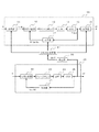
図1は、本発明の第1の実施例に係るPLL回路の構成を示すブロック図である。図1において、PLL回路は、固定基準クロックを生成するPLL回路10と、所定の周波数レンジ内で出力信号周波数を変化させて(例えばスイープさせて)出力するPLL回路20と、PLL回路20の出力周波数を検出し予め設定した所定の周波数と比較する検出器30と、分周比を設定する信号をPLL回路10に出力する分周比設定回路40とを備える。
FIG. 1 is a block diagram showing a configuration of a PLL circuit according to a first embodiment of the present invention. In FIG. 1, the PLL circuit includes a
PLL回路10は、1/M(Mは正の整数)分周を行う分周器11、位相比較器12、チャージポンプ13、ローパスフィルタ(LPF)14、電圧制御発振器(VCO)15、1/P(Pは正の整数)分周を行う分周器16、1/N1(N1は正の整数)分周を行う分周器17を備える。分周器11は、PLL回路10に入力される基準発振入力信号(周波数fr)を1/Mに分周して、位相比較器12の一方の入力端に出力する。一方、VCO15の発振出力信号(周波数P・fo1)が分周器17によって1/N1に分周され、分周信号(周波数P・fo1/N1)が位相比較器12の他方の入力端に入力される。位相比較器12は、VCO15の分周信号と分周器11の出力信号との位相を比較し、比較結果に基づいてチャージポンプ13を駆動する。チャージポンプ13の出力信号は、LPF14において積分され、直流電圧に変換され、VCO15に出力される。この直流電圧は、VCO15の発振周波数(周波数P・fo1)を制御するためのコントロール電圧である。分周器16は、VCO15の発振出力信号を1/Pに分周して、出力信号(周波数fo1)を出力する。
The
このような構成のPLL回路10は、VCO15、分周器17、位相比較器12のフィードバックループによってPLL回路10の出力信号の周波数fo1が所望の周波数f1に設定(ロック)される。すなわち、fo1(=f1)=N1・fr/(M・P)となる。ここで、分周器11の分周比1/M、分周器16の分周比1/P、および分周器17の分周比1/N1は、分周比設定回路40によって変更可能とされる。
In the
一方、PLL回路20は、位相比較器22、チャージポンプ23、LPF24、VCO25、1/N2(N2は正の整数)分周を行う分周器27を備える。PLL回路20では、VCO25の発振出力信号(周波数fo2)が分周器27によって1/N2に分周され、分周信号(周波数fo2/N2)が位相比較器22の一方の入力端に入力される。位相比較器22は、VCO25の分周信号とPLL回路20の入力比較信号(周波数fi)との位相を比較し、比較結果に基づいてチャージポンプ23を駆動する。チャージポンプ23の出力信号は、LPF24において積分され、直流電圧に変換され、VCO25に出力される。この直流電圧は、VCO25の発振周波数fo2を制御するためのコントロール電圧である。VCO25の出力信号がPLL回路20の出力信号となる。
On the other hand, the
このような構成のPLL回路20において、VCO25、分周器27、位相比較器22のフィードバックループによってPLL回路20の出力信号の周波数fo2と周波数fiとがロックする。すなわち、fo2=N2*fiとなる。なお、VCO25の出力信号の周波数fo2がPLL回路10の出力信号の周波数fo1の整数倍または整数分の一の周波数を含むような範囲において、入力比較信号の周波数fiが変化するものとする。
In the
検出器30は、PLL回路10の出力信号における所望の出力周波数f1とPLL回路20の出力信号の出力周波数fo2とを比較し、比較結果に基づいて分周比設定回路40に分周比コントロール信号CNTを出力する。分周比設定回路40は、分周比コントロール信号CNTによってPLL回路10における分周比を設定する。具体的には、PLL回路20の出力周波数fo2がPLL回路10における出力周波数fo1の整数倍または整数分の一の近傍にならないように、すなわち基本波および高調波の関係とならないように、分周器11、16、17の少なくとも一つの分周器における分周比を変更する。すなわち、整数N1、M、Pの少なくとも一つを変更する。
The
ここで、PLL回路10の出力周波数fo1の変更方法について説明する。図2は、PLL回路10、20の周波数スペクトル特性を示す図である。図2において、PLL回路10のPLL帯域幅をfc1、PLL回路20のPLL帯域幅をfc2、先に述べた第1の閾値をft1とする。この時、図2(a)に示すように、|fo1−fo2|≦ft1=fc1+fc2であれば、PLL回路10とPLL回路20のPLL帯域が重なり合って、PLL回路間に干渉が生じてしまう。この場合には、図2(b)に示すように、|fo1−fo2|>ft1=fc1+fc2となるようにPLL回路10の出力周波数fo1を変更する。このように変更することで、PLL帯域同士の重なりが無くなってPLL回路間の干渉を抑えることが可能となる。
Here, a method of changing the output frequency fo1 of the
さらに、PLL回路10の出力周波数は、基準クロックとして許された範囲、すなわちクロック信号の周波数可変許容範囲で変更されるようにする。図3は、PLL回路10の出力周波数の変更方法を示す図である。図3において、先に述べた第2の閾値をft2とする。ここで、例えばPLL回路20の出力周波数fo2が上昇してPLL回路10の出力周波数fo1に接近し、|fo1−fo2|=ft1となったとする。この場合に、PLL回路10の出力周波数fo1を周波数可変許容範囲に収まる、例えばfo1−ft2に変更するようにする。
Further, the output frequency of the
図4は、本発明の第1の実施例に係るPLL回路の動作を示すフローチャートである。PLL回路10の出力信号における出力周波数fo1が基準クロックとして所望される周波数f1にロックしている状態であるとする(ステップS11)。検出器30は、周波数可変であるPLL回路20の出力周波数fo2をモニタし(ステップS12)、PLL回路20の出力周波数fo2がPLL回路10における所望の周波数f1の整数倍または整数分の一の近傍になったか否かを判別する(ステップS13)。ステップS13で近傍ではないと判別される場合、ステップS12、S13を繰り返す。ステップS13で近傍であると判別された場合、検出器30が分周比設定回路40の制御を行う分周比コントロール信号CNTを分周比設定回路40に出力する。分周比設定回路40は、PLL回路10における分周比を切り替える。分周比の切り替えによって、PLL回路10の出力周波数fo1は、基準クロックとして許された範囲であって、且つ、f1の整数倍または整数分の一の近傍ではない周波数f2に切り替わる(ステップS14)。
FIG. 4 is a flowchart showing the operation of the PLL circuit according to the first exemplary embodiment of the present invention. Assume that the output frequency fo1 in the output signal of the
本実施例のPLL回路は、以上のように動作し、PLL回路10の周波数を基準クロック信号として許される範囲内であって、かつPLL回路10の所望の周波数f1とPLL回路20の出力周波数fo2とが相互に整数倍(基本波および高調波関係)の近傍にはならない範囲となるように制御する。このような制御によってPLL回路の出力周波数同士が整数倍の近傍にならないので、PLL回路間のスプリアスノイズ等の干渉を防ぎ、スプリアスノイズ等の干渉に起因するPLLジッタの悪化を防ぐことができる。
The PLL circuit of the present embodiment operates as described above, and the frequency of the
以上説明したようなPLL回路は、例えば光ディスク装置等に適用される。光ディスク装置において、PLL回路10の出力信号は、装置のシステムクロック信号、例えばDRAMのクロック信号として用いられる。また、PLL回路20は、光ディスクの記録または再生におけるデータの書き込みまたは読み出し周波数に追従して動作し、出力信号の周波数が変動するPLL回路20の出力信号は、光ディスクのアクセスに必要なクロック信号として用いられる。このような光ディスク装置では、システムクロック信号の周波数の整数倍が光ディスクの記録または再生における信号の周波数の可変範囲内に存在することが起こりうる。これに対して本実施例のPLL回路を適用することで、PLL帯域内でのスプリアスノイズ等の干渉を抑え、信頼性の高い光ディスク装置を提供することができる。
The PLL circuit as described above is applied to, for example, an optical disc apparatus. In the optical disc apparatus, the output signal of the
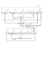
図5は、本発明の第2の実施例に係るPLL回路の構成を示すブロック図である。図5において、図1と同一の符号は、同一物を表し、その説明を省略する。図5に示すPLL回路は、図1における検出器30の替わりに、PLL回路10、20の出力信号を入力する周波数比較器50を備える。周波数比較器50は、PLL回路10の出力周波数fo1とPLL回路20の出力周波数fo2とを比較し、比較結果に基づいて分周比設定回路40に分周比コントロール信号CNTを出力する。分周比設定回路40は、分周比コントロール信号CNTによってPLL回路10の分周比を設定する。
FIG. 5 is a block diagram showing a configuration of a PLL circuit according to the second embodiment of the present invention. 5, the same reference numerals as those in FIG. 1 represent the same items, and the description thereof is omitted. The PLL circuit shown in FIG. 5 includes a
図6は、本発明の第2の実施例に係るPLL回路の動作を示すフローチャートである。図6において、図4と同一の符号のステップは、同一処理を表し、その説明を省略する。周波数比較器50でPLL回路10の出力周波数fo1と周波数可変であるPLL回路20の出力周波数fo2とをモニタする(ステップS22)。PLL回路20の出力周波数fo2がPLL回路10の出力周波数fo1の整数倍または整数分の一の近傍になったか否か判別する(ステップS23)。ステップS23で近傍ではないと判別される場合、ステップS22、S23を繰り返す。ステップS23で近傍であると判別された場合、周波数比較器50が分周比設定回路40の制御を行う分周比コントロール信号CNTを分周比設定回路40に送信し、分周比設定回路40がPLL回路10の分周比を切り替える。分周比の切り替えによって、PLL回路10の出力周波数fo1は、基準クロックとして許された範囲であって、且つ、f1の整数倍または整数分の一の近傍ではない周波数f2に切り替わる(ステップS24)。
FIG. 6 is a flowchart showing the operation of the PLL circuit according to the second exemplary embodiment of the present invention. In FIG. 6, steps with the same reference numerals as those in FIG. The
以上のように第2の実施例に係るPLL回路は、第1の実施例と同様に、PLL回路10の出力周波数fo1とPLL回路20の出力周波数fo2とが相互に整数倍の近傍にならないように制御される。したがって、PLL回路間のスプリアスノイズ等の干渉を防ぎ、スプリアスノイズ等の干渉に起因するPLLジッタの悪化を防ぐことができる。
As described above, in the PLL circuit according to the second embodiment, similarly to the first embodiment, the output frequency fo1 of the
以上本発明を上記実施例に即して説明したが、本発明は、上記実施例にのみ限定されるものではなく、本願特許請求の範囲の各請求項の発明の範囲内で当業者であればなし得るであろう各種変形、修正を含むことは勿論である。 The present invention has been described with reference to the above-described embodiments. However, the present invention is not limited to the above-described embodiments, and those skilled in the art within the scope of the invention of each claim of the present application claims. It goes without saying that various modifications and corrections that can be made are included.
10、20 PLL回路
11、16、17、27 分周器
12、22 位相比較器
13、23 チャージポンプ
14、24 ローパスフィルタ(LPF)
15、25 電圧制御発振器(VCO)
30 検出器
40 分周比設定回路
50 周波数比較器
10, 20
15, 25 Voltage controlled oscillator (VCO)
30 detector 40 division
Claims (21)
前記第2のPLL回路の出力信号周波数と所定の周波数との差が第1の閾値以下であるか否かを検出する検出器と、
前記差が前記第1の閾値以下である場合に、前記第1のPLL回路の出力信号周波数を、前記第1の閾値より大きい第2の閾値以下であって前記第1の閾値より大きくなる範囲で変更する周波数設定回路と、
を備えることを特徴とするPLL回路。 In a PLL circuit that configures at least a first and a second PLL (Phase Locked Loop) circuit on the same device,
A detector for detecting whether a difference between an output signal frequency of the second PLL circuit and a predetermined frequency is equal to or less than a first threshold;
A range in which the output signal frequency of the first PLL circuit is equal to or less than a second threshold value greater than the first threshold value and greater than the first threshold value when the difference is equal to or less than the first threshold value. Frequency setting circuit to be changed in
A PLL circuit comprising:
2つの入力端に入力される信号の位相差に応じて出力信号を出力する位相比較器と、
前記位相比較器の出力信号における低域成分信号の大きさに対応した周波数で発振して出力信号を出力する電圧制御発振器と、
入力参照クロック信号を分周して前記位相比較器の一方の入力端に出力する第1の分周器と、
前記電圧制御発振器の出力信号を分周して前記位相比較器の他方の入力端に出力する第2の分周器と、
前記電圧制御発振器の出力信号を分周して前記第1のPLL回路の出力信号を出力する第3の分周器と、
を備え、
前記周波数設定回路は、前記第1、第2、第3の分周器における少なくとも一つの分周比を変更することを特徴とする請求項9または10記載のPLL回路。 The first PLL circuit includes:
A phase comparator that outputs an output signal in accordance with a phase difference between signals input to two input terminals;
A voltage controlled oscillator that oscillates at a frequency corresponding to the magnitude of the low-frequency component signal in the output signal of the phase comparator and outputs the output signal;
A first frequency divider that divides the input reference clock signal and outputs it to one input terminal of the phase comparator;
A second frequency divider that divides the output signal of the voltage controlled oscillator and outputs it to the other input terminal of the phase comparator;
A third frequency divider that divides the output signal of the voltage controlled oscillator and outputs the output signal of the first PLL circuit;
With
11. The PLL circuit according to claim 9, wherein the frequency setting circuit changes at least one division ratio in the first, second, and third frequency dividers.
前記第2のPLL回路の出力信号周波数と所定の周波数との差が第1の閾値以下であるか否かを検出し、前記差が前記第1の閾値以下である場合に、前記第1のPLL回路の出力信号周波数を、前記第1の閾値より大きい第2の閾値以下であって前記第1の閾値より大きくなる範囲で変更することを特徴とするPLL回路の干渉防止方法。 In the PLL circuit interference prevention method in which at least the first and second PLL (Phase Locked Loop) circuits are configured on the same device,
It is detected whether or not a difference between an output signal frequency of the second PLL circuit and a predetermined frequency is equal to or less than a first threshold, and when the difference is equal to or less than the first threshold, the first An interference prevention method for a PLL circuit, wherein the output signal frequency of the PLL circuit is changed within a range that is equal to or smaller than a second threshold value that is greater than the first threshold value and greater than the first threshold value.
Priority Applications (4)
| Application Number | Priority Date | Filing Date | Title |
|---|---|---|---|
| JP2006122057A JP2007295363A (en) | 2006-04-26 | 2006-04-26 | Pll circuit, method for preventing interference of the pll circuit, and optical disk device having pll circuit mounted thereon |
| US11/738,931 US20070254600A1 (en) | 2006-04-26 | 2007-04-23 | Pll circuit, method for preventing interference between pll circuits, and optical disk apparatus comprising the pll circuit |
| KR1020070040983A KR100894236B1 (en) | 2006-04-26 | 2007-04-26 | PLL circuit, method of preventing interference of the PLL circuit and optical-disk apparatus having the PLL circuit |
| CNA2007101010443A CN101064511A (en) | 2006-04-26 | 2007-04-26 | Pll circuit, method of preventing interference of the pll circuit and optical-disk apparatus having the pll circuit |
Applications Claiming Priority (1)
| Application Number | Priority Date | Filing Date | Title |
|---|---|---|---|
| JP2006122057A JP2007295363A (en) | 2006-04-26 | 2006-04-26 | Pll circuit, method for preventing interference of the pll circuit, and optical disk device having pll circuit mounted thereon |
Publications (1)
| Publication Number | Publication Date |
|---|---|
| JP2007295363A true JP2007295363A (en) | 2007-11-08 |
Family
ID=38648923
Family Applications (1)
| Application Number | Title | Priority Date | Filing Date |
|---|---|---|---|
| JP2006122057A Pending JP2007295363A (en) | 2006-04-26 | 2006-04-26 | Pll circuit, method for preventing interference of the pll circuit, and optical disk device having pll circuit mounted thereon |
Country Status (4)
| Country | Link |
|---|---|
| US (1) | US20070254600A1 (en) |
| JP (1) | JP2007295363A (en) |
| KR (1) | KR100894236B1 (en) |
| CN (1) | CN101064511A (en) |
Cited By (3)
| Publication number | Priority date | Publication date | Assignee | Title |
|---|---|---|---|---|
| JP2013046392A (en) * | 2011-08-26 | 2013-03-04 | Toshiba Corp | Integrated circuit |
| US9641113B2 (en) | 2014-02-28 | 2017-05-02 | General Electric Company | System and method for controlling a power generation system based on PLL errors |
| JP2017228891A (en) * | 2016-06-21 | 2017-12-28 | 日本システムウエア株式会社 | Pll incorporated device and pll interference prevention method |
Families Citing this family (5)
| Publication number | Priority date | Publication date | Assignee | Title |
|---|---|---|---|---|
| JP5463246B2 (en) * | 2010-09-01 | 2014-04-09 | 株式会社日立製作所 | Phase synchronization circuit, CDR circuit, and reception circuit |
| JP2014241471A (en) * | 2013-06-11 | 2014-12-25 | セイコーエプソン株式会社 | Signal generating circuit, signal generating device, process of manufacturing the same, electronic apparatus, and mobile body |
| US10263624B2 (en) * | 2017-06-27 | 2019-04-16 | Intel IP Corporation | Phase synchronization between two phase locked loops |
| US11588489B1 (en) | 2021-10-06 | 2023-02-21 | Shaoxing Yuanfang Semiconductor Co., Ltd. | Obtaining lock in a phase-locked loop (PLL) upon being out of phase-lock |
| US11923864B2 (en) | 2021-10-18 | 2024-03-05 | Shaoxing Yuanfang Semiconductor Co., Ltd. | Fast switching of output frequency of a phase locked loop (PLL) |
Citations (3)
| Publication number | Priority date | Publication date | Assignee | Title |
|---|---|---|---|---|
| JPH1116295A (en) * | 1997-06-23 | 1999-01-22 | Matsushita Electric Ind Co Ltd | Optical disk device |
| JP2000068829A (en) * | 1998-08-25 | 2000-03-03 | Mitsubishi Electric Corp | Frequency synthesizer circuit |
| JP2001309135A (en) * | 2000-04-24 | 2001-11-02 | Canon Inc | Signal processor, and signal processing method |
Family Cites Families (3)
| Publication number | Priority date | Publication date | Assignee | Title |
|---|---|---|---|---|
| JP3527593B2 (en) | 1996-08-08 | 2004-05-17 | 株式会社ルネサステクノロジ | Phased locked loop circuit |
| US6952138B2 (en) | 2001-09-12 | 2005-10-04 | Telefonaktiebolaget Lm Ericsson (Publ) | Generation of a phase locked loop output signal having reduced spurious spectral components |
| US6970030B1 (en) * | 2003-10-01 | 2005-11-29 | Silicon Laboratories, Inc. | Dual phased-locked loop structure having configurable intermediate frequency and reduced susceptibility to interference |
-
2006
- 2006-04-26 JP JP2006122057A patent/JP2007295363A/en active Pending
-
2007
- 2007-04-23 US US11/738,931 patent/US20070254600A1/en not_active Abandoned
- 2007-04-26 KR KR1020070040983A patent/KR100894236B1/en not_active IP Right Cessation
- 2007-04-26 CN CNA2007101010443A patent/CN101064511A/en active Pending
Patent Citations (3)
| Publication number | Priority date | Publication date | Assignee | Title |
|---|---|---|---|---|
| JPH1116295A (en) * | 1997-06-23 | 1999-01-22 | Matsushita Electric Ind Co Ltd | Optical disk device |
| JP2000068829A (en) * | 1998-08-25 | 2000-03-03 | Mitsubishi Electric Corp | Frequency synthesizer circuit |
| JP2001309135A (en) * | 2000-04-24 | 2001-11-02 | Canon Inc | Signal processor, and signal processing method |
Cited By (3)
| Publication number | Priority date | Publication date | Assignee | Title |
|---|---|---|---|---|
| JP2013046392A (en) * | 2011-08-26 | 2013-03-04 | Toshiba Corp | Integrated circuit |
| US9641113B2 (en) | 2014-02-28 | 2017-05-02 | General Electric Company | System and method for controlling a power generation system based on PLL errors |
| JP2017228891A (en) * | 2016-06-21 | 2017-12-28 | 日本システムウエア株式会社 | Pll incorporated device and pll interference prevention method |
Also Published As
| Publication number | Publication date |
|---|---|
| KR20070105923A (en) | 2007-10-31 |
| US20070254600A1 (en) | 2007-11-01 |
| KR100894236B1 (en) | 2009-04-20 |
| CN101064511A (en) | 2007-10-31 |
Similar Documents
| Publication | Publication Date | Title |
|---|---|---|
| KR100894236B1 (en) | PLL circuit, method of preventing interference of the PLL circuit and optical-disk apparatus having the PLL circuit | |
| US8446194B2 (en) | Spread spectrum clock generating circuit | |
| US20120287967A1 (en) | Pll circuit, communication device, and loopback test method of communication device | |
| US9484948B2 (en) | Clock generation circuit | |
| KR100374648B1 (en) | Phase locked loop circuit for reducing electromagnetic interference and control method thereof | |
| JP2012195826A (en) | Spread spectrum clock generation circuit | |
| US9280928B2 (en) | Apparatus and method for driving LED display | |
| US8988122B2 (en) | Apparatus and method for performing spread-spectrum clock control | |
| KR20100077990A (en) | Apparatus and method for small size spread spectrum clock generation | |
| KR100819390B1 (en) | Frequency synthesizer using two phase locked loop | |
| US9019016B2 (en) | Accumulator-type fractional N-PLL synthesizer and control method thereof | |
| JP2007208367A (en) | Synchronizing signal generating apparatus, transmitter, and control method | |
| JP2013200135A (en) | Radar transceiver | |
| JP2007124508A (en) | Pll transient response control system and communication system | |
| JP3548557B2 (en) | Fractional-N frequency synthesizer | |
| US6181758B1 (en) | Phase-locked loop with small phase error | |
| JPH08256058A (en) | Signal generator | |
| US20150188552A1 (en) | Phase locked loop and control method thereof | |
| US7574185B2 (en) | Method and apparatus for generating a phase-locked output signal | |
| JP2015222918A (en) | Fractional PLL circuit | |
| JP2010045443A (en) | Carrier wave generation circuit | |
| JP2006005523A (en) | Method for reducing fractional spurious, fractional n-pll oscillator reducing generation of fractional spurious | |
| GB2368207A (en) | PLL circuit and frequency division method reducing spurious noise | |
| JP2005151444A (en) | Frequency synthesizer | |
| JP2002141797A (en) | Frequency synthesizer |
Legal Events
| Date | Code | Title | Description |
|---|---|---|---|
| A621 | Written request for application examination |
Free format text: JAPANESE INTERMEDIATE CODE: A621 Effective date: 20090310 |
|
| A977 | Report on retrieval |
Free format text: JAPANESE INTERMEDIATE CODE: A971007 Effective date: 20101118 |
|
| A131 | Notification of reasons for refusal |
Free format text: JAPANESE INTERMEDIATE CODE: A131 Effective date: 20101130 |
|
| A02 | Decision of refusal |
Free format text: JAPANESE INTERMEDIATE CODE: A02 Effective date: 20110419 |