JP2007281131A - Resin mold coil - Google Patents

Resin mold coil Download PDF

Info

Publication number
JP2007281131A
JP2007281131A JP2006104130A JP2006104130A JP2007281131A JP 2007281131 A JP2007281131 A JP 2007281131A JP 2006104130 A JP2006104130 A JP 2006104130A JP 2006104130 A JP2006104130 A JP 2006104130A JP 2007281131 A JP2007281131 A JP 2007281131A
Authority
JP
Japan
Prior art keywords
electrostatic shield
coil
resin
shield layer
unit
Prior art date
Legal status (The legal status is an assumption and is not a legal conclusion. Google has not performed a legal analysis and makes no representation as to the accuracy of the status listed.)
Pending
Application number
JP2006104130A
Other languages
Japanese (ja)
Inventor
Teruhiko Maeda
照彦 前田
Yoshikazu Takeuchi
美和 竹内
Hiroshi Sonobe
浩 園部
Satoshi Kida
聡 木田
Yusuke Shima
裕介 陦
Current Assignee (The listed assignees may be inaccurate. Google has not performed a legal analysis and makes no representation or warranty as to the accuracy of the list.)
Toshiba Corp
Toshiba Industrial Products and Systems Corp
Original Assignee
Toshiba Corp
Toshiba Industrial Products Manufacturing Corp
Priority date (The priority date is an assumption and is not a legal conclusion. Google has not performed a legal analysis and makes no representation as to the accuracy of the date listed.)
Filing date
Publication date
Application filed by Toshiba Corp, Toshiba Industrial Products Manufacturing Corp filed Critical Toshiba Corp
Priority to JP2006104130A priority Critical patent/JP2007281131A/en
Publication of JP2007281131A publication Critical patent/JP2007281131A/en
Pending legal-status Critical Current

Links

Images

Landscapes

  • Insulating Of Coils (AREA)
  • Regulation Of General Use Transformers (AREA)

Abstract

<P>PROBLEM TO BE SOLVED: To provide a resin-molded coil in which a partial discharge hardly occurs. <P>SOLUTION: A winding wire is formed by winding an insulating coated conductor. The wire is molded with resin into a unit coil (2), and an electrostatic shielding layer (3) of conductor is formed on the surface of the unit coil (2). Two or more of the unit coil (2) covered with the electrostatic shielding layer (3) are arranged at a prescribed interval in an axial direction and connected in series. The whole of assemblies is molded with resin into a cylindrical object. <P>COPYRIGHT: (C)2008,JPO&INPIT

Description

本発明は変圧器、リアクトル等の誘導機器に用いる樹脂モールドコイルに関する。   The present invention relates to a resin molded coil used for induction devices such as transformers and reactors.

変圧器、リアクトル等の誘導機器に用いるコイルとして、図11の断面図に示すようにコイル周囲を絶縁樹脂でモールドした構造の樹脂モールドコイル50が広く用いられている。この樹脂モールドコイル50は絶縁被覆銅線あるいは絶縁被覆銅帯をドーナツ状に巻回した単位コイル51を最初に製作し、次にそれらを複数個軸方向に積み重ねてモールド型内に固定し、最後に全体を熱硬化性樹脂でモールドして製作される。複数個の単位コイル51の接続方法は用途により異なるが、高圧機器用のものでは一般に直列接続される。この樹脂モールドコイル50は、絶縁性、難燃性に優れた特性を示す他、コンパクトに製作できる利点がある。   As a coil used for induction devices such as a transformer and a reactor, a resin-molded coil 50 having a structure in which the periphery of the coil is molded with an insulating resin as shown in a sectional view of FIG. 11 is widely used. This resin mold coil 50 is manufactured by first producing a unit coil 51 in which an insulation-coated copper wire or insulation-coated copper strip is wound in a donut shape, and then stacking them in the axial direction and fixing them in a mold. The whole is molded by thermosetting resin. The connection method of the plurality of unit coils 51 differs depending on the application, but is generally connected in series for high-voltage equipment. The resin mold coil 50 has an advantage that it can be manufactured in a compact manner in addition to exhibiting excellent properties of insulation and flame retardancy.

モールドのため注型された樹脂は単位コイル51を構成する銅線あるいは銅帯の隙間にも入り込み、それら導体間の絶縁性を高める。しかし、単位コイル51は銅線あるいは銅帯を密に巻回して形成されているため導体間の狭い隙間には樹脂は侵入しにくい。このため単位コイル51内に樹脂が未含浸の隙間が残ったり、例え含浸しても導体と樹脂との間に微小な空隙が残ったりすることがある。   The resin cast for molding enters the gap between the copper wires or the copper strips constituting the unit coil 51, and improves the insulation between these conductors. However, since the unit coil 51 is formed by densely winding a copper wire or a copper band, the resin hardly enters a narrow gap between conductors. For this reason, a gap in which the resin is not impregnated may remain in the unit coil 51, or a minute gap may remain between the conductor and the resin even if impregnated.

単位コイル51に高電圧が印加されると、単位コイル51と接地間、あるいは単位コイル相互間に電位差が生じて高電界が発生する。発生する電界の強さは、電束密度が同じであれば誘電率に反比例する。空隙部分の誘電率は樹脂より低いため、空隙内の電界強度は樹脂部分の4〜5倍にもなる。その値が空気の絶縁破壊電界強度を上回ると空隙内で部分放電が発生し、故障につながる。   When a high voltage is applied to the unit coil 51, a potential difference is generated between the unit coil 51 and the ground or between the unit coils to generate a high electric field. The strength of the generated electric field is inversely proportional to the dielectric constant if the electric flux density is the same. Since the dielectric constant of the void portion is lower than that of the resin, the electric field strength in the void is 4 to 5 times that of the resin portion. If the value exceeds the breakdown electric field strength of air, partial discharge occurs in the air gap, leading to failure.

こうした問題を解決する従来技術として、例えば特許文献1には注入樹脂の粘度を小さくして樹脂中に空隙が残ることを防止する技術が開示されている。また、特許文献2には樹脂モールド層の表面に導電性高分子からなる表面導電層を設けて耐クラック性や耐部分放電性を向上させる技術が開示されている。また、特許文献3には、変圧器に雷インパルスが侵入した場合には給電端子に近い単位コイルに最も高い電圧が加わることから、給電端子に近い単位コイルの内周側を覆う絶縁部の肉厚を他の単位コイル内周側を覆う部分より厚くする技術が開示されている。   As a conventional technique for solving such a problem, for example, Patent Document 1 discloses a technique for reducing the viscosity of an injected resin to prevent voids from remaining in the resin. Patent Document 2 discloses a technique for improving crack resistance and partial discharge resistance by providing a surface conductive layer made of a conductive polymer on the surface of a resin mold layer. Further, in Patent Document 3, when the lightning impulse enters the transformer, the highest voltage is applied to the unit coil close to the power supply terminal, so that the thickness of the insulating portion covering the inner peripheral side of the unit coil close to the power supply terminal is disclosed. A technique is disclosed in which the thickness is made thicker than the portion covering the inner peripheral side of another unit coil.

しかしながら特別高圧級の変圧器に使用する樹脂モールドコイルとしては、上記のような対策だけでは不十分であり、部分放電の発生を防止するための更なる技術が求められている。
特開平08−316055号公報 特開平08−264347号公報 特開平07−122439号公報
However, as a resin mold coil used for a special high voltage class transformer, the above-mentioned measures are not sufficient, and further techniques for preventing the occurrence of partial discharge are required.
Japanese Patent Laid-Open No. 08-316055 JP 08-264347 A Japanese Patent Application Laid-Open No. 07-122439

本発明はこのような従来技術の問題点を解決するためになされたもので、その課題は、部分放電が発生しにくい樹脂モールドコイルを提供することにある。   The present invention has been made to solve such problems of the prior art, and an object thereof is to provide a resin molded coil in which partial discharge is unlikely to occur.

前記課題を解決するための請求項1に記載の発明は、絶縁被覆導体を巻回してなる巻線を樹脂モールドして略環状に形成した単位コイル(2)の表面には導体による静電シールド層(3)が形成してあり、静電シールド層が形成された単位コイルは複数個を軸方向に所定の間隔をおいて配置して直列接続してあり、それら複数個の単位コイルは全体を樹脂モールドして筒状に仕上げてあることを特徴とする樹脂モールドコイルである。   According to a first aspect of the present invention for solving the above-described problem, the surface of the unit coil (2) formed by resin molding a winding formed by winding an insulation-coated conductor and formed into a substantially annular shape is an electrostatic shield made of a conductor. The unit coil on which the layer (3) is formed and the electrostatic shield layer is formed is arranged in series with a plurality of unit coils arranged at predetermined intervals in the axial direction. This is a resin-molded coil that is molded into a cylinder by resin molding.

このように単位コイルの周りに静電シールド層を設けると、静電シールド層の電位は単位コイルを構成する各巻線の電位のほぼ平均値となる。そのため、各巻線と静電シールド層との間の電位差が小さくなる。また、静電シールド層内の巻線間の電位差も小さくなる。これらのことから、微小空隙が静電シールド層内の単位コイル周りに存在したとしても部分放電が生じにくくなる効果を奏する。   When the electrostatic shield layer is provided around the unit coil as described above, the potential of the electrostatic shield layer is approximately an average value of the potential of each winding constituting the unit coil. Therefore, the potential difference between each winding and the electrostatic shield layer is reduced. Also, the potential difference between the windings in the electrostatic shield layer is reduced. For these reasons, even if a minute gap exists around the unit coil in the electrostatic shield layer, the partial discharge is less likely to occur.

更に、静電シールド層を設けたことにより、樹脂モールドコイルに立ち上がりの速いサージ電圧が加わった場合の各単位コイルにかかる電圧が平均化される。これにより樹脂モールドコイルの入力端子に近い位置に接続された単位コイルに他より著しく高い電圧が加わることがなくなる。従って、それら単位コイル付近での部分放電も抑制される効果を奏する。   Further, by providing the electrostatic shield layer, the voltage applied to each unit coil when a surge voltage with a fast rise is applied to the resin molded coil is averaged. As a result, a voltage significantly higher than the others is not applied to the unit coil connected to a position near the input terminal of the resin mold coil. Therefore, there is an effect that partial discharge in the vicinity of these unit coils is also suppressed.

また、請求項2に記載の発明は、請求項1に記載の樹脂モールドコイルにおいて、該樹脂モールドコイルの表面には表面接地用の表面導体層(30)が形成してあることを特徴とする樹脂モールドコイルである。   The invention according to claim 2 is the resin molded coil according to claim 1, wherein a surface conductor layer (30) for surface grounding is formed on the surface of the resin molded coil. It is a resin mold coil.

このような表面導体層を形成して接地すれば、装置の安全性を高めることができる。表面導体層の形成により静電シールド層から接地までの距離が短くなるが、静電シールド層の外側のモールド層には微小隙間は形成されないので部分放電が発生する心配は少ない。   If such a surface conductor layer is formed and grounded, the safety of the apparatus can be improved. Although the distance from the electrostatic shield layer to the ground is shortened by the formation of the surface conductor layer, a minute gap is not formed in the mold layer outside the electrostatic shield layer, so there is little fear of partial discharge.

また、請求項3に記載の発明は、請求項1又は2に記載の樹脂モールドコイルにおいて、前記複数個の単位コイルにおける隣り合う前記静電シールド層間にはコンデンサ(19)が接続してあり、それらコンデンサも複数個の単位コイルと一体に樹脂モールドしてあることを特徴とする樹脂モールドコイルである。   Moreover, the invention according to claim 3 is the resin molded coil according to claim 1 or 2, wherein a capacitor (19) is connected between the adjacent electrostatic shield layers in the plurality of unit coils. These capacitors are also resin-molded coils that are integrally resin-molded with a plurality of unit coils.

このような構成の樹脂モールドコイルは、請求項1に記載の樹脂モールドコイルと同様の効果を奏する。更に、コンデンサを追加したことによりサージ電圧が加わった場合における樹脂モールドコイルの入力端子近くに接続された単位コイル近傍の電界強度が一層弱まる。従って、それら単位コイル近傍に微小な空隙が存在したとしても部分放電が一層生じにくくなる効果を奏する。   The resin molded coil having such a configuration has the same effect as the resin molded coil according to claim 1. Furthermore, the addition of a capacitor further weakens the electric field strength near the unit coil connected near the input terminal of the resin mold coil when a surge voltage is applied. Therefore, even if a minute gap exists in the vicinity of these unit coils, there is an effect that partial discharge is less likely to occur.

また、請求項4に記載の発明は、請求項1又は2に記載の樹脂モールドコイルにおいて、隣り合う前記単位コイル間の渡り配線(20)周りにおいて隣り合う前記静電シールド層を接近して対向させることにより隣り合う静電シールド層間の静電容量を増加させてあることを特徴とする樹脂モールドコイルである。
このような構成の樹脂モールドコイルは、請求項3に記載の樹脂モールドコイルと同様の効果を奏する。
According to a fourth aspect of the present invention, in the resin-molded coil according to the first or second aspect, the adjacent electrostatic shield layers are brought close to each other around the connecting wire (20) between the adjacent unit coils. In this resin mold coil, the electrostatic capacitance between adjacent electrostatic shield layers is increased.
The resin molded coil having such a configuration has the same effects as the resin molded coil according to claim 3.

また、請求項5に記載の発明は、請求項3に記載の樹脂モールドコイルにおいて、隣り合う前記静電シールド層間に接続する前記コンデンサ(19)のリード線の静電シールド層への接続位置(25)は隣り合うコンデンサについて同じ位置にしてあることを特徴とする樹脂モールドコイルである。   The invention according to claim 5 is the resin molded coil according to claim 3, wherein the lead wire of the capacitor (19) connected between the adjacent electrostatic shield layers is connected to the electrostatic shield layer ( 25) is a resin-molded coil characterized in that adjacent capacitors are located at the same position.

本構成のように隣り合う上下のコンデンサのリード線を共通の接続点にて静電シールド層3に接続してあれば、コンデンサを渡って流れるサージ電流が静電シールド層を流れなくなる。従って、静電シールド層上の電位分布がサージ電流によって乱されることが少なくなり、静電シールド層内に強電界部分が発生しにくくなる。これにより部分放電の発生が抑制される。   If lead wires of adjacent upper and lower capacitors are connected to the electrostatic shield layer 3 at a common connection point as in this configuration, surge current flowing across the capacitor will not flow through the electrostatic shield layer. Therefore, the potential distribution on the electrostatic shield layer is less likely to be disturbed by the surge current, and a strong electric field portion is less likely to be generated in the electrostatic shield layer. Thereby, generation | occurrence | production of partial discharge is suppressed.

また、請求項6に記載の発明は、請求項3又は5に記載の樹脂モールドコイルにおいて、前記コンデンサ(19)を隣り合う前記静電シールド層間に複数個接続してあることを特徴とする樹脂モールドコイルである。   The invention according to claim 6 is the resin molded coil according to claim 3 or 5, wherein a plurality of the capacitors (19) are connected between the adjacent electrostatic shield layers. It is a molded coil.

小容量のコンデンサを環状の静電シールド層の周りに複数個配置すれば、静電シールド層上の電位分布を一層安定させることができる。従って、部分放電が一層発生しにくくなる効果を奏する。   If a plurality of small-capacitance capacitors are arranged around the annular electrostatic shield layer, the potential distribution on the electrostatic shield layer can be further stabilized. Therefore, there is an effect that partial discharge is less likely to occur.

以下、本発明に係る樹脂モールドコイルの構成例を実施形態に分けて説明する。
(第1の実施形態)
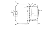
図1は、第1の実施形態に係る樹脂モールドコイル1の構成を断面図で示したものである。樹脂モールドコイル1は全体として略円筒または略角筒の筒状に形成されており、筒の中心孔に変圧器の鉄心、リアクトルの鉄心等を通して使用される。
Hereinafter, the structural example of the resin mold coil which concerns on this invention is divided into embodiment, and is demonstrated.
(First embodiment)
FIG. 1 is a cross-sectional view showing the configuration of a resin molded coil 1 according to the first embodiment. The resin mold coil 1 is formed in a generally cylindrical or substantially rectangular tube shape as a whole, and is used through the center hole of the tube through a transformer iron core, a reactor iron core, or the like.

図1は、その筒状樹脂モールドコイル1の中心軸を含む断面の片側部分を示している。樹脂モールドコイル1は、単位コイルと呼ぶ略環状をなすコイル2を複数個つないで形成してある。単位コイル2は絶縁被覆銅線を略環状に巻回し、絶縁性樹脂で全体をモールドしたものである。絶縁被覆銅線の代わりに絶縁した銅帯を用いてもよい。   FIG. 1 shows one side portion of a cross section including the central axis of the cylindrical resin molded coil 1. The resin mold coil 1 is formed by connecting a plurality of substantially circular coils 2 called unit coils. The unit coil 2 is formed by winding an insulating coated copper wire in a substantially annular shape and molding the whole with an insulating resin. An insulated copper band may be used instead of the insulation-coated copper wire.

本実施形態の樹脂モールドコイル1の特徴として、モールド形成した各単位コイル2の表面には静電シールド層3が形成してある。静電シールド層3は、比較的電気抵抗の高い導電性テープを巻回して形成してある。導電性テープの代わりに導電塗料の塗布、金属の溶射により静電シールド層3を形成してもよい。   As a feature of the resin molded coil 1 of this embodiment, an electrostatic shield layer 3 is formed on the surface of each molded unit coil 2. The electrostatic shield layer 3 is formed by winding a conductive tape having a relatively high electrical resistance. Instead of the conductive tape, the electrostatic shield layer 3 may be formed by applying a conductive paint or spraying metal.

表面に静電シールド層3を形成した単位コイル2は、複数個が軸方向に所定の間隔をおいて配置してある。そして、それらは渡り配線(20)により直列接続してある。各静電シールド層3は独立しており、他と絶縁された状態になっている。複数個の単位コイル2は、そのように配置した状態で全体を樹脂でモールドして筒状に仕上げてある。軸方向両端に位置する単位コイルからはリード線5、6が外部に引き出してある。   A plurality of unit coils 2 having the electrostatic shield layer 3 formed on the surface thereof are arranged at predetermined intervals in the axial direction. And they are connected in series by a crossover wiring (20). Each electrostatic shield layer 3 is independent and is insulated from the others. The plurality of unit coils 2 are molded into a cylindrical shape by resin as a whole in such a state. Lead wires 5 and 6 are drawn out from unit coils located at both ends in the axial direction.

このように本実施形態の樹脂モールドコイル1は、図11に示した従来の樹脂モールドコイル50と比較すると、各単位コイル2の表面に電気的に他と絶縁された静電シールド層3が形成してあることに特徴がある。   As described above, in the resin molded coil 1 of this embodiment, the electrostatic shield layer 3 that is electrically insulated from the other is formed on the surface of each unit coil 2 as compared with the conventional resin molded coil 50 shown in FIG. It is characterized by being.

次に、このように各単位コイル2の表面に静電シールド層3を形成した効果について説明する。図2は、本実施形態の樹脂モールドコイル1の電気的な等価回路である。各単位コイル2は直列接続されており、両端の単位コイル2はリード線5、6により外部の入力端子7、8に接続してある。各単位コイル2は絶縁された静電シールド層3により個々にシールドされている。   Next, the effect of forming the electrostatic shield layer 3 on the surface of each unit coil 2 will be described. FIG. 2 is an electrical equivalent circuit of the resin molded coil 1 of the present embodiment. Each unit coil 2 is connected in series, and the unit coils 2 at both ends are connected to external input terminals 7 and 8 by lead wires 5 and 6. Each unit coil 2 is individually shielded by an insulated electrostatic shield layer 3.

この状態で入力端子7、8に高電圧Vが印加されたとする。単位コイル2の数をn個とすると、各単位コイル2の両端に位置する巻線間にはV/nの高い電位差が生ずる。両端以外の巻線と、同じ単位コイル2内の他の巻線との間にもV/nほどではないが高い電位差が生ずる。   Assume that a high voltage V is applied to the input terminals 7 and 8 in this state. If the number of unit coils 2 is n, a high potential difference of V / n is generated between the windings located at both ends of each unit coil 2. A high potential difference is generated between the windings other than both ends and other windings in the same unit coil 2, although not as high as V / n.

更に、各巻線と隣の単位コイル2の巻線との間にも高い電位差が生ずる。ここで、静電シールド層3が形成されていない図11の樹脂モールドコイル50の場合を考える。単位コイル2を構成する各巻線の物理的配置は図11に示すようになっている。こうした配置のため隣り合う単位コイル2に属し、高電位差を持つ2つの巻線が接近して配置されることになる。例として図11における巻線53、54は別の単位コイル2に属し、その間にはV/nより大きな電位差が生じている。   Further, a high potential difference is generated between each winding and the winding of the adjacent unit coil 2. Here, consider the case of the resin molded coil 50 of FIG. 11 in which the electrostatic shield layer 3 is not formed. The physical arrangement of the windings constituting the unit coil 2 is as shown in FIG. Because of this arrangement, two windings belonging to adjacent unit coils 2 and having a high potential difference are arranged close to each other. As an example, the windings 53 and 54 in FIG. 11 belong to another unit coil 2, and a potential difference larger than V / n is generated between them.

こうした巻線間の電位差の他に、各巻線と接地との間にも高い電位差が生じている。これは、印加電圧Vの入力線が接地(中性点)に対して高い電位差を有しているからである。   In addition to the potential difference between the windings, a high potential difference is also generated between each winding and the ground. This is because the input line of the applied voltage V has a high potential difference with respect to the ground (neutral point).

このように樹脂モールドコイル50の両端に高電圧が印加されると、各巻線は、同じ単位コイル51内の他の巻線、他の単位コイル51の巻線、更には接地との間に高い電位差を持つことになる。その電位差をその間の距離で割った値が電界である。その電界の大きさが、その間にある絶縁物の絶縁破壊電界を超えると部分放電が発生する。   Thus, when a high voltage is applied to both ends of the resin mold coil 50, each winding is high between the other winding in the same unit coil 51, the winding of the other unit coil 51, and further to the ground. It will have a potential difference. A value obtained by dividing the potential difference by the distance between them is an electric field. When the magnitude of the electric field exceeds the dielectric breakdown electric field of the insulator between them, partial discharge occurs.

図11に示した従来構造の樹脂モールドコイル50では、こうした巻線間、巻線と接地間の電位差が局所的に大きくなる個所が生じやすい。「背景技術」で述べたように、単位コイル51を構成する巻線間にはモールド樹脂が侵入しにくい。そのため微小な空隙が残りやすい。残った微小空隙に上に述べたような高電界が加わると、微小空隙内に残る気体が絶縁破壊を起こして部分放電が発生する。その微小空隙が例え真空であったとしても、その真空空間を通って部分放電が発生する。   In the resin-molded coil 50 having the conventional structure shown in FIG. 11, such a portion where the potential difference between the windings and between the winding and the ground is locally large is likely to occur. As described in “Background Art”, it is difficult for mold resin to enter between windings constituting the unit coil 51. Therefore, minute gaps are likely to remain. When a high electric field as described above is applied to the remaining microvoids, the gas remaining in the microvoids causes dielectric breakdown and partial discharge occurs. Even if the minute gap is a vacuum, a partial discharge is generated through the vacuum space.

そうした微小空隙における部分放電の発生を防ぐには、巻線間、巻線と接地間の電位差を小さくしてやればよい。本実施形態の各単位コイル2の表面に設けた静電シールド層3は、この電位差を小さくして微小空隙での部分放電の発生を防ぐことを目的としている。   In order to prevent the occurrence of partial discharge in such a minute gap, the potential difference between the windings and between the winding and the ground may be reduced. The electrostatic shield layer 3 provided on the surface of each unit coil 2 of the present embodiment aims to reduce this potential difference and prevent the occurrence of partial discharge in a minute gap.

単位コイル2の表面に静電シールド層3を設けた場合、単位コイル2を構成する巻線と静電シールド層3との間にはモールド樹脂を挟んでコンデンサが形成される。その状態を電気的等価回路で示せば、図3に示すように無数の微小容量浮遊コンデンサ10が存在していることになる。単位コイル2の巻線と静電シールド層3との間隔は狭く形成してある。単位コイル2の巻線と静電シールド層3との間隔が狭く、且つその間に浮遊コンデンサ10が存在すると、導体である静電シールド層3の電位は各巻線の電位のほぼ平均値となる。   When the electrostatic shield layer 3 is provided on the surface of the unit coil 2, a capacitor is formed with a mold resin interposed between the windings constituting the unit coil 2 and the electrostatic shield layer 3. If this state is shown by an electrical equivalent circuit, there are innumerable microcapacitance floating capacitors 10 as shown in FIG. The distance between the winding of the unit coil 2 and the electrostatic shield layer 3 is narrow. When the interval between the winding of the unit coil 2 and the electrostatic shield layer 3 is narrow and the floating capacitor 10 exists between them, the potential of the electrostatic shield layer 3 as a conductor is almost the average value of the potential of each winding.

単位コイル2の周りにこのような各巻線の平均電位をもつ静電シールド層3が存在すると、各巻線と静電シールド層3との間の電位差は、各単位コイル2の両端間の電位差V/nの1/2以下の小さい値となる。従って、微小空隙が静電シールド層3内側の単位コイル2内に存在したとしても、巻線と静電シールド層3の間では放電は生じにくくなる。   When the electrostatic shield layer 3 having such an average potential of each winding exists around the unit coil 2, the potential difference between each winding and the electrostatic shield layer 3 is the potential difference V between both ends of each unit coil 2. A small value of 1/2 or less of / n. Therefore, even if a minute gap exists in the unit coil 2 inside the electrostatic shield layer 3, it is difficult for discharge to occur between the winding and the electrostatic shield layer 3.

また、こうした各巻線の平均電位をもつ静電シールド層3が周囲に存在すると、同じ単位コイル2に属する巻線間の電位差も大きくなりにくい。その値は静電シールド層3が存在しない場合に比べて小さくなる。従って、同じ単位コイル2に属する巻線間での放電も生じにくくなる。   Further, when the electrostatic shield layer 3 having the average potential of each winding is present in the periphery, the potential difference between windings belonging to the same unit coil 2 is not easily increased. The value is smaller than when the electrostatic shield layer 3 is not present. Accordingly, it is difficult for electric discharge to occur between windings belonging to the same unit coil 2.

静電シールド層3の外側部分については、静電シールド層3と接地との間に高い電位差が生じる。しかし、静電シールド層3の外側部分の樹脂層には微小空隙は殆ど存在しない。且つ、静電シールド層3は同電位である。このため静電シールド層3が形成されていない場合と違って、静電シールド層3の外側部分における電界強度はどの部分も同じ程度となり、局所的に高い電界が発生するという現象は生じない。従って、静電シールド層3の外側部分では、部分放電は殆ど発生しない。   For the outer portion of the electrostatic shield layer 3, a high potential difference is generated between the electrostatic shield layer 3 and the ground. However, there are almost no microvoids in the resin layer outside the electrostatic shield layer 3. In addition, the electrostatic shield layer 3 has the same potential. For this reason, unlike the case where the electrostatic shield layer 3 is not formed, the electric field strength in the outer portion of the electrostatic shield layer 3 is almost the same in all portions, and the phenomenon that a high electric field is locally generated does not occur. Therefore, the partial discharge hardly occurs in the outer portion of the electrostatic shield layer 3.

このような理由から本実施形態の樹脂モールドコイル1では、静電シールド層3を設けたことにより局所的に高電界となる部分が生じない。従って、単位コイル2内に微小な空隙が存在したとしても部分放電が発生しにくくなる効果を奏する。   For this reason, in the resin molded coil 1 of the present embodiment, the provision of the electrostatic shield layer 3 does not cause a portion where a high electric field is locally generated. Therefore, even if a minute gap exists in the unit coil 2, there is an effect that partial discharge hardly occurs.

更に、後述する第2以降の実施形態における効果との関係で、静電シールド層3を設けた場合の別の効果について説明する。その効果は、樹脂モールドコイル1にサージ電圧が加わった場合の各単位コイル2に加わる電圧の不均一性についてのものである。   Furthermore, another effect when the electrostatic shield layer 3 is provided will be described in relation to the effect in the second and subsequent embodiments described later. The effect is related to the non-uniformity of the voltage applied to each unit coil 2 when a surge voltage is applied to the resin mold coil 1.

図4は、静電シールド層3が設けられていない場合(図11の従来構造の樹脂モールドコイル50に相当)に、立ち上がりの速いサージ電圧が加わった場合の主要な電流経路を示したものである。図中には、主要な浮遊コンデンサも記載してある。浮遊コンデンサには、隣り合う単位コイル2間の浮遊コンデンサ12と、各単位コイル2と接地GND間の浮遊コンデンサ13とがある。   FIG. 4 shows a main current path when a surge voltage having a fast rise is applied when the electrostatic shield layer 3 is not provided (corresponding to the resin mold coil 50 having the conventional structure in FIG. 11). is there. The main stray capacitors are also shown in the figure. The floating capacitors include a floating capacitor 12 between adjacent unit coils 2 and a floating capacitor 13 between each unit coil 2 and the ground GND.

立ち上がりの速いサージ電圧に対しては、単位コイル2のインピーダンスは大きく、浮遊コンデンサ12、13のインピーダンスは逆に小さくなる。このため、立ち上がりの速いサージ電圧が入力端子7、8間に印加された場合には、サージ電流は単位コイル2を通しては流れず、大略、図中の電流経路15又は16を通って流れる。電流経路15は、直列につながる浮遊コンデンサ12を渡って流れる経路である。電流経路16は、単位コイル2と接地GND間の浮遊コンデンサ13を通って一旦、接地GNDに流れ、その後、再び単位コイル2と接地GND間の浮遊コンデンサ13を通って反対側入力端子に流れる経路である。   For a surge voltage that rises quickly, the impedance of the unit coil 2 is large, and the impedances of the floating capacitors 12 and 13 are conversely small. For this reason, when a surge voltage having a fast rise is applied between the input terminals 7 and 8, the surge current does not flow through the unit coil 2, but generally flows through the current path 15 or 16 in the figure. The current path 15 is a path that flows across the floating capacitors 12 connected in series. The current path 16 temporarily flows to the ground GND through the floating capacitor 13 between the unit coil 2 and the ground GND, and then flows again to the opposite input terminal through the floating capacitor 13 between the unit coil 2 and the ground GND. It is.

ここで、各単位コイル2の両端に加わる電圧について考察する。便宜上、各浮遊コンデンサ12の容量は等しく、各浮遊コンデンサ13の容量も等しいとする。各浮遊コンデンサ13の容量をゼロとした場合には、各浮遊コンデンサ12に加わる電圧、即ち、各単位コイル2の両端に加わる電圧は等しい値となる。即ち、サージ電圧は各単位コイル2によって均等にかかる。   Here, the voltage applied to both ends of each unit coil 2 will be considered. For convenience, it is assumed that the capacity of each floating capacitor 12 is equal and the capacity of each floating capacitor 13 is also equal. When the capacitance of each floating capacitor 13 is zero, the voltage applied to each floating capacitor 12, that is, the voltage applied to both ends of each unit coil 2 is equal. That is, the surge voltage is applied equally by each unit coil 2.

ところが、実際には単位コイル2と接地GNDとの間には浮遊コンデンサ13が存在する。浮遊コンデンサ13が存在すると図7の入力端子7より流れ込んだ電流の一部は、入力端子7に近い位置の浮遊コンデンサ13を通って接地GNDに流れ込む。そして、接地GNDを流れた後、反対側の入力端子8に近い位置の浮遊コンデンサ13を通って入力端子8に流出する。そのため、入力端子7、8に近い位置に接続された単位コイル2間の浮遊コンデンサ12には比較的大きな電流が流れる。これに対し、中央に近い位置に接続された単位コイル2間の浮遊コンデンサ12には少ない電流しか流れない。   However, there is actually a floating capacitor 13 between the unit coil 2 and the ground GND. If the floating capacitor 13 is present, a part of the current flowing from the input terminal 7 in FIG. 7 flows to the ground GND through the floating capacitor 13 located near the input terminal 7. Then, after flowing through the ground GND, it flows out to the input terminal 8 through the floating capacitor 13 at a position close to the input terminal 8 on the opposite side. Therefore, a relatively large current flows through the floating capacitor 12 between the unit coils 2 connected to positions close to the input terminals 7 and 8. On the other hand, only a small current flows through the floating capacitor 12 between the unit coils 2 connected at a position close to the center.

各単位コイル2にかかる電圧は、その部分の浮遊コンデンサ12のインピーダンスにそこを流れる電流の値を掛けたものである。従って、大きな電流が流れる入力端子7、8に近い位置に接続された単位コイル2にかかる電圧は大きくなり、中央に近い位置に接続された単位コイル2にかかる電圧は小さくなる。即ち、単位コイル2にかかる電圧に不均一が生ずる。その不均一さは接地GNDとの間の浮遊コンデンサ13の容量が増すに従って強くなり、反対に単位コイル2間の浮遊コンデンサ12の容量が増すと弱くなる。   The voltage applied to each unit coil 2 is obtained by multiplying the impedance of the floating capacitor 12 in that portion by the value of the current flowing therethrough. Therefore, the voltage applied to the unit coil 2 connected to a position close to the input terminals 7 and 8 through which a large current flows increases, and the voltage applied to the unit coil 2 connected to a position close to the center decreases. That is, nonuniformity occurs in the voltage applied to the unit coil 2. The non-uniformity becomes stronger as the capacitance of the floating capacitor 13 between the ground coil and the ground GND increases, and decreases as the capacitance of the floating capacitor 12 between the unit coils 2 increases.

このようにサージ電圧が加わった場合には、入力端子7、8の近くに接続された単位コイル2には大きな電圧がかかり、その付近の微小空隙に部分放電が生じやすい。この部分放電を防ぐには、各単位コイル2に加わる電圧を均等化し、一部の単位コイル2にのみ不均一な大きな電圧がかかるのを防止する必要がある。それには、図4における電流経路15を流れる電流は大きく、電流経路16を流れる電流は小さくなくように工夫してやればよい。それには前述したように、単位コイル2と接地GNDとの間の浮遊コンデンサ13の容量は小さく、単位コイル2間の浮遊コンデンサ12の容量は大きくしてやればよい。   When a surge voltage is applied in this way, a large voltage is applied to the unit coil 2 connected in the vicinity of the input terminals 7 and 8, and partial discharge is likely to occur in a minute gap in the vicinity thereof. In order to prevent this partial discharge, it is necessary to equalize the voltage applied to each unit coil 2 and prevent a nonuniform large voltage from being applied only to some of the unit coils 2. For this purpose, it is sufficient to devise so that the current flowing through the current path 15 in FIG. 4 is large and the current flowing through the current path 16 is not small. For this purpose, as described above, the capacitance of the floating capacitor 13 between the unit coil 2 and the ground GND is small, and the capacitance of the floating capacitor 12 between the unit coils 2 may be increased.

ここで、再び本実施形態の図1に示した樹脂モールドコイル1の構造に戻ると、図4に相当する等価回路は図5に示すようになる。図4における単位コイル2間の浮遊コンデンサ12に対応するコンデンサは、図5の等価回路では単位コイル2の巻線と静電シールド層3との間の浮遊コンデンサ17と、隣り合う静電シールド層3間の浮遊コンデンサ18とを直列接続したものである。単位コイル2と静電シールド層3との間隔は狭く形成してある。従って、単位コイル2と静電シールド層3間の浮遊コンデンサ17の容量は非常に大きな値となっている。また、隣り合う静電シールド層3は、図1に示すように大きな面積部分が接近して対向した状態になっている。従って、隣り合う静電シールド層3間の浮遊コンデンサ18の値も非常に大きな値となっている。   Here, when returning to the structure of the resin molded coil 1 shown in FIG. 1 of the present embodiment, the equivalent circuit corresponding to FIG. 4 is as shown in FIG. The capacitor corresponding to the floating capacitor 12 between the unit coils 2 in FIG. 4 is the floating capacitor 17 between the winding of the unit coil 2 and the electrostatic shield layer 3 in the equivalent circuit of FIG. A floating capacitor 18 between 3 is connected in series. The interval between the unit coil 2 and the electrostatic shield layer 3 is formed narrow. Therefore, the capacitance of the floating capacitor 17 between the unit coil 2 and the electrostatic shield layer 3 is a very large value. Moreover, the adjacent electrostatic shield layers 3 are in a state where large area portions approach each other as shown in FIG. Therefore, the value of the floating capacitor 18 between the adjacent electrostatic shield layers 3 is also a very large value.

これに対して静電シールド層3が設けてない図4の等価回路における単位コイル2間の浮遊コンデンサ12では、コンデンサの電極に相当する巻線間の距離が長く、対向する部分の面積も小さい。そのため、その容量は小さな値となっている。   On the other hand, in the floating capacitor 12 between the unit coils 2 in the equivalent circuit of FIG. 4 in which the electrostatic shield layer 3 is not provided, the distance between the windings corresponding to the electrode of the capacitor is long and the area of the facing portion is small. . Therefore, the capacity is a small value.

こうしたことから、図5の等価回路における隣り合う単位コイル2間の静電容量である浮遊コンデンサ17、18の直列容量は、図4における隣り合う単位コイル2間の浮遊コンデンサ12の容量よりも大きくなる。従って、サージ電圧が加わった場合に図5の等価回路の電流経路15を流れる電流は、図4の回路の電流経路15を流れる電流よりも大きくなる。その結果、前述したような理由により各単位コイル2に加わる電圧は図4の回路の場合よりも均等化され、入力端子7、8近くの単位コイル2間に特別大きな電圧が加わることがなくなる。   For this reason, the series capacitance of the floating capacitors 17 and 18, which is the capacitance between the adjacent unit coils 2 in the equivalent circuit of FIG. 5, is larger than the capacitance of the floating capacitor 12 between the adjacent unit coils 2 in FIG. Become. Therefore, when a surge voltage is applied, the current flowing through the current path 15 of the equivalent circuit of FIG. 5 is larger than the current flowing through the current path 15 of the circuit of FIG. As a result, the voltage applied to each unit coil 2 is equalized as compared with the case of the circuit of FIG. 4 for the reasons described above, and no particularly large voltage is applied between the unit coils 2 near the input terminals 7 and 8.

単位コイル2間に加わる電圧が低くなれば、単位コイル2と静電シールド層3間の電圧も低くなる。その電圧が低くなれば、静電シールド層3の内側部分の電界強度も弱まる。従って、静電シールド層3内に微小な空隙が残っていたとしても部分放電が生じにくくなる。   If the voltage applied between the unit coils 2 decreases, the voltage between the unit coils 2 and the electrostatic shield layer 3 also decreases. If the voltage is lowered, the electric field strength at the inner portion of the electrostatic shield layer 3 is also weakened. Therefore, even if a minute gap remains in the electrostatic shield layer 3, partial discharge is less likely to occur.

このように本実施形態の樹脂モールドコイル1では、静電シールド層3を設けたことにより単位コイル2内の電界強度が弱くなる。そのため、それら単位コイル2の巻線近傍に微小な空隙が残っていたとしても部分放電が生じにくくなる効果を奏する。   Thus, in the resin mold coil 1 of this embodiment, the electric field strength in the unit coil 2 is weakened by providing the electrostatic shield layer 3. Therefore, even if a minute gap remains in the vicinity of the windings of these unit coils 2, there is an effect that partial discharge is less likely to occur.

(第2の実施形態)
図6に、第2の実施形態に係る樹脂モールドコイル1aの構成を断面図で示す。本実施形態の樹脂モールドコイル1aは、図1に示した第1の実施形態に係る樹脂モールドコイル1の隣り合う静電シールド層3間にコンデンサ19を追加したものである。その等価回路は図7に示すようになる。追加したコンデンサ19は、隣り合う静電シールド層3間の浮遊コンデンサ18に並列につながり、隣り合う静電シールド層3間の静電容量を増加させる。
(Second Embodiment)
In FIG. 6, the structure of the resin mold coil 1a which concerns on 2nd Embodiment is shown with sectional drawing. In the resin molded coil 1a of this embodiment, a capacitor 19 is added between adjacent electrostatic shield layers 3 of the resin molded coil 1 according to the first embodiment shown in FIG. The equivalent circuit is as shown in FIG. The added capacitor 19 is connected in parallel to the floating capacitor 18 between the adjacent electrostatic shield layers 3 and increases the capacitance between the adjacent electrostatic shield layers 3.

隣り合う静電シールド層3間の静電容量が増加すると、第1の実施形態で述べたように、樹脂モールドコイル1aの入力端子7、8間にサージ電圧が加わった場合に電流経路15を流れる電流が増加する。それにより各単位コイル2に加わる電圧は均等化される方向に向かい、入力端子7、8近くに接続した単位コイル2間に加わる電圧は低くなる。   When the electrostatic capacitance between the adjacent electrostatic shield layers 3 increases, as described in the first embodiment, when a surge voltage is applied between the input terminals 7 and 8 of the resin molded coil 1a, the current path 15 is changed. The flowing current increases. As a result, the voltage applied to each unit coil 2 tends to be equalized, and the voltage applied between the unit coils 2 connected near the input terminals 7 and 8 becomes low.

その結果、単位コイル2と静電シールド層3間の電圧も低くなり、静電シールド層3の内側部分の電界強度も弱まる。それにより静電シールド層3内では部分放電が生じにくくなる。   As a result, the voltage between the unit coil 2 and the electrostatic shield layer 3 is also reduced, and the electric field strength at the inner portion of the electrostatic shield layer 3 is also reduced. Thereby, partial discharge is less likely to occur in the electrostatic shield layer 3.

このように本実施形態の樹脂モールドコイル1aでは、コンデンサ19を追加したことによりサージ電圧が加わった場合における入力端子7、8近くの単位コイル2近傍の電界強度が一層弱まる。従って、それら単位コイル2近傍に微小な空隙が残っていたとしても部分放電が一層生じにくくなる効果を奏する。   Thus, in the resin mold coil 1a of this embodiment, the addition of the capacitor 19 further weakens the electric field strength near the unit coil 2 near the input terminals 7 and 8 when a surge voltage is applied. Therefore, even if minute gaps remain in the vicinity of these unit coils 2, there is an effect that partial discharge is less likely to occur.

(第3の実施形態)
図8に、第3の実施形態に係る樹脂モールドコイル1bの構成を断面図で示す。本実施形態の樹脂モールドコイル1bが図6に示した樹脂モールドコイル1aと異なる点は、隣り合う静電シールド層3間に設けるコンデンサ19の形成の仕方にある。本実施形態では、単位コイル2間の渡り配線20周りにおいて隣り合う静電シールド層3を接近して対向させ、それにより隣り合う静電シールド層間の静電容量を増加させている。この場合の等価回路は、図7に示したものと同じとなる。
(Third embodiment)
In FIG. 8, the structure of the resin mold coil 1b which concerns on 3rd Embodiment is shown with sectional drawing. The resin molded coil 1b of the present embodiment is different from the resin molded coil 1a shown in FIG. 6 in the manner of forming the capacitor 19 provided between the adjacent electrostatic shield layers 3. In the present embodiment, adjacent electrostatic shield layers 3 around the crossover wiring 20 between the unit coils 2 are brought close to each other, thereby increasing the capacitance between adjacent electrostatic shield layers. The equivalent circuit in this case is the same as that shown in FIG.

隣り合う静電シールド層3間にこのようなコンデンサ19aを形成すれば、第2の実施形態の場合と同様にサージ電圧が加わった場合における入力端子7、8近くの単位コイル2近傍の電界強度が一層弱まる。従って、それら単位コイル2近傍に微小な空隙が残っていたとしても部分放電が一層生じにくくなる効果を奏する。   If such a capacitor 19a is formed between the adjacent electrostatic shield layers 3, the electric field strength in the vicinity of the unit coil 2 near the input terminals 7 and 8 when a surge voltage is applied as in the case of the second embodiment. Is further weakened. Therefore, even if minute gaps remain in the vicinity of these unit coils 2, there is an effect that partial discharge is less likely to occur.

(第4の実施形態)
図9に、第4の実施形態に係る樹脂モールドコイル1cの構成を断面図で示す。本実施形態の樹脂モールドコイル1cは、図6に示した第2の実施形態に係る樹脂モールドコイル1aの変形実施形態である。図6に示した構成と異なる点は、隣り合う静電シールド層3間に追加したコンデンサ19の静電シールド層3への接続位置にある。
(Fourth embodiment)
In FIG. 9, the structure of the resin mold coil 1c which concerns on 4th Embodiment is shown with sectional drawing. The resin mold coil 1c of this embodiment is a modified embodiment of the resin mold coil 1a according to the second embodiment shown in FIG. The difference from the configuration shown in FIG. 6 is the connection position of the capacitor 19 added between the adjacent electrostatic shield layers 3 to the electrostatic shield layer 3.

図6に示した構成では、1個の静電シールド層3に接続する上下2個のコンデンサ19のリード線を、静電シールド層3上の別々の位置25a、25bで接続している。これに対して本実施形態では図9中の接続点25に示すように、上下のコンデンサ19のリード線を共通の接続点25にて静電シールド層3に接続している。即ち、共通の一点で接続している。   In the configuration shown in FIG. 6, the lead wires of the upper and lower capacitors 19 connected to one electrostatic shield layer 3 are connected at different positions 25 a and 25 b on the electrostatic shield layer 3. On the other hand, in this embodiment, the lead wires of the upper and lower capacitors 19 are connected to the electrostatic shield layer 3 at a common connection point 25 as indicated by a connection point 25 in FIG. That is, they are connected at a common point.

上下のコンデンサ19のリード線が別々の位置で静電シールド層3に接続されていると、サージ電圧の印加により図5の電流経路15を流れるサージ電流が静電シールド層3をも通って流れることになる。   When the lead wires of the upper and lower capacitors 19 are connected to the electrostatic shield layer 3 at different positions, a surge current flowing through the current path 15 in FIG. 5 flows through the electrostatic shield layer 3 by applying a surge voltage. It will be.

各静電シールド層3は環状をなしていて、単位コイル2を一次コイルと考えると各静電シールド層3は1ターンの二次巻線を構成している。そのため、単位コイル2に電流を流すと静電シールド層3にも電流が流れて発熱をもたらす。また、その電流は樹脂モールドコイル1b、1cの中心孔に通した鉄心内に発生する磁束を弱める働きもする。この静電シールド層3に流れる電流を少なくするため、静電シールド層3は比抵抗の値がある程度高い導体で形成される。   Each electrostatic shield layer 3 has an annular shape, and when the unit coil 2 is considered as a primary coil, each electrostatic shield layer 3 forms a secondary winding of one turn. Therefore, when a current is passed through the unit coil 2, a current also flows through the electrostatic shield layer 3 to generate heat. The current also serves to weaken the magnetic flux generated in the iron core passing through the center holes of the resin mold coils 1b and 1c. In order to reduce the current flowing through the electrostatic shield layer 3, the electrostatic shield layer 3 is formed of a conductor having a certain value of specific resistance.

従って、図6のような構成の場合には、接続点25a、25b間の静電シールド層3上を、コンデンサ19を渡るサージ電流が流れてその間に電位差を発生させる。その電位差は静電シールド層3上の電位分布を乱し、静電シールド層3内に強電界部分を生じさせることがある。強電界部分では部分放電が生じ易い。   Therefore, in the case of the configuration as shown in FIG. 6, a surge current flows across the capacitor 19 on the electrostatic shield layer 3 between the connection points 25a and 25b, and a potential difference is generated therebetween. The potential difference disturbs the potential distribution on the electrostatic shield layer 3 and may cause a strong electric field portion in the electrostatic shield layer 3. Partial discharge is likely to occur in a strong electric field portion.

これに対して図9に示す本実施形態の構成では、上下のコンデンサ19のリード線が共通の接続点25にて静電シールド層3に接続されている。そのため、コンデンサ19を渡って流れるサージ電流は、静電シールド層3上を流れることはない。従って、静電シールド層3上の電位分布がそれによって乱されないため、静電シールド層3内に強電界部分が生じにくい。その結果として部分放電が生じにくくなる効果が得られる。   On the other hand, in the configuration of this embodiment shown in FIG. 9, the lead wires of the upper and lower capacitors 19 are connected to the electrostatic shield layer 3 at a common connection point 25. Therefore, the surge current that flows across the capacitor 19 does not flow on the electrostatic shield layer 3. Therefore, the electric potential distribution on the electrostatic shield layer 3 is not disturbed thereby, so that a strong electric field portion is hardly generated in the electrostatic shield layer 3. As a result, an effect that partial discharge is less likely to occur is obtained.

なお、図9の構成の場合も、単位コイル2の巻線と静電シールド層3との間には図7に示した浮遊コンデンサ17が存在するため、その浮遊コンデンサ17を流れた電流は静電シールド層3内を流れて接続点25に達する。その流れる過程で静電シールド層3上に電位差を生じさせる。その電位差を小さくするには、コンデンサ19が接続された接続点25までの距離を短くすればよい。   In the case of the configuration of FIG. 9 also, the floating capacitor 17 shown in FIG. 7 exists between the winding of the unit coil 2 and the electrostatic shield layer 3, so that the current flowing through the floating capacitor 17 is static. It flows through the electric shield layer 3 and reaches the connection point 25. A potential difference is generated on the electrostatic shield layer 3 in the flow process. In order to reduce the potential difference, the distance to the connection point 25 to which the capacitor 19 is connected may be shortened.

こうしたことから、隣り合う静電シールド層3には大きな容量のコンデンサ19を1個接続する代わりに、小容量のコンデンサを環状の静電シールド層3の周りに等間隔に複数個配置することが望ましい。そのように配置すれば、静電シールド層3上の電位分布を図9に示した場合よりも一層安定させることができ、部分放電の発生を一層効果的に抑えることができる。   For this reason, a plurality of small-capacitance capacitors can be arranged around the annular electrostatic shield layer 3 at equal intervals instead of connecting one large-capacitance capacitor 19 to the adjacent electrostatic shield layer 3. desirable. With such an arrangement, the potential distribution on the electrostatic shield layer 3 can be more stabilized than in the case shown in FIG. 9, and the occurrence of partial discharge can be more effectively suppressed.

(その他の実施形態)
前記、第1〜第4の実施形態における各樹脂モールドコイルの外表面には、表面導体層を更に形成してもよい。図10は、第1の実施形態に係る樹脂モールドコイル1の表面に、そのような表面導体層30を形成した場合の断面図である。そのような表面導体層30は、比較的電気抵抗の高い導電性テープの巻回か、導電塗料の塗布、金属の溶射により形成する。そして、使用に当ってはその表面導体層30を接地する。それによって安全性を高めることができる。
(Other embodiments)
A surface conductor layer may be further formed on the outer surface of each resin molded coil in the first to fourth embodiments. FIG. 10 is a cross-sectional view when such a surface conductor layer 30 is formed on the surface of the resin molded coil 1 according to the first embodiment. Such a surface conductor layer 30 is formed by winding a conductive tape having a relatively high electrical resistance, applying a conductive paint, or spraying a metal. In use, the surface conductor layer 30 is grounded. Thereby, safety can be increased.

樹脂モールドコイル1dの外表面にこのような接地した表面導体層30を設けた場合には、単位コイル2周囲の静電シールド層3から接地までの距離が短くなる。しかし、静電シールド層3より外側のモールド層には微小隙間は形成されにくいので、その部分で部分放電の発生することは殆ど起こらない。   When such a grounded surface conductor layer 30 is provided on the outer surface of the resin mold coil 1d, the distance from the electrostatic shield layer 3 around the unit coil 2 to the ground is shortened. However, since a minute gap is hardly formed in the mold layer outside the electrostatic shield layer 3, partial discharge hardly occurs in that portion.

第1の実施形態に係る樹脂モールドコイル1の断面図である。It is sectional drawing of the resin mold coil 1 which concerns on 1st Embodiment. 第1の実施形態に係る樹脂モールドコイル1の等価回路である。It is an equivalent circuit of the resin mold coil 1 which concerns on 1st Embodiment. 静電シールド層3を有する単位コイル2内の浮遊コンデンサの状態である。This is a state of a floating capacitor in the unit coil 2 having the electrostatic shield layer 3. 静電シールド層3を有しない樹脂モールドコイルにサージ電圧が加わった場合の主要な電流経路を説明する図である。It is a figure explaining the main electric current path | route when a surge voltage is added to the resin mold coil which does not have the electrostatic shield layer. 第1の実施形態に係る樹脂モールドコイル1にサージ電圧が加わった場合の主要な電流経路を説明する図である。It is a figure explaining the main electric current path | route when a surge voltage is added to the resin mold coil 1 which concerns on 1st Embodiment. 第2の実施形態に係る樹脂モールドコイル1aの断面図である。It is sectional drawing of the resin mold coil 1a which concerns on 2nd Embodiment. 第2の実施形態に係る樹脂モールドコイル1aの等価回路と電流経路を説明する図である。It is a figure explaining the equivalent circuit and electric current path | route of the resin mold coil 1a which concern on 2nd Embodiment. 第3の実施形態に係る樹脂モールドコイル1bの断面図である。It is sectional drawing of the resin mold coil 1b which concerns on 3rd Embodiment. 第4の実施形態に係る樹脂モールドコイル1cの断面図である。It is sectional drawing of the resin mold coil 1c which concerns on 4th Embodiment. 外表面に静電シールド層30を設けた樹脂モールドコイル1dの断面図である。It is sectional drawing of the resin mold coil 1d which provided the electrostatic shield layer 30 on the outer surface. 従来技術に係る図1相当図である。FIG. 2 is a view corresponding to FIG.

符号の説明Explanation of symbols

図面中、1、1a、1b、1c、1dは樹脂モールドコイル、2は単位コイル、3は静電シールド層、19はコンデンサ、25は共通の接続点、30は表面導体層を示す。   In the drawings, 1, 1a, 1b, 1c, 1d are resin molded coils, 2 is a unit coil, 3 is an electrostatic shield layer, 19 is a capacitor, 25 is a common connection point, and 30 is a surface conductor layer.

Claims (6)

絶縁被覆導体を巻回してなる巻線を樹脂モールドして略環状に形成した単位コイル(2)は表面に導体による静電シールド層(3)が形成してあり、静電シールド層が形成された単位コイルは複数個を軸方向に所定の間隔をおいて配置して直列接続してあり、それら複数個の単位コイルは全体を樹脂モールドして筒状に仕上げてあることを特徴とする樹脂モールドコイル。   The unit coil (2), which is formed in a substantially annular shape by resin-molding a winding formed by winding an insulating coating conductor, has an electrostatic shield layer (3) formed of a conductor on the surface, and the electrostatic shield layer is formed. A plurality of unit coils are arranged in series with a predetermined interval in the axial direction, and the plurality of unit coils are resin-molded and finished into a cylindrical shape. Mold coil. 請求項1に記載の樹脂モールドコイルにおいて、該樹脂モールドコイルの表面には表面接地用の表面導体層(30)が形成してあることを特徴とする樹脂モールドコイル。   The resin mold coil according to claim 1, wherein a surface conductor layer (30) for surface grounding is formed on a surface of the resin mold coil. 請求項1又は2に記載の樹脂モールドコイルにおいて、前記複数個の単位コイルにおける隣り合う前記静電シールド層間にはコンデンサ(19)が接続してあり、それらコンデンサも複数個の単位コイルと一体に樹脂モールドしてあることを特徴とする樹脂モールドコイル。   3. The resin molded coil according to claim 1, wherein a capacitor (19) is connected between the adjacent electrostatic shield layers of the plurality of unit coils, and the capacitors are also integrated with the plurality of unit coils. A resin-molded coil which is resin-molded. 請求項1又は2に記載の樹脂モールドコイルにおいて、隣り合う前記単位コイル間の渡り配線(20)周りにおいて隣り合う前記静電シールド層を接近して対向させることにより隣り合う静電シールド層間の静電容量を増加させてあることを特徴とする樹脂モールドコイル。   3. The resin molded coil according to claim 1, wherein the electrostatic shield layers adjacent to each other around the connecting wire (20) between the adjacent unit coils are brought close to each other to face each other and static electricity between the adjacent electrostatic shield layers is static. A resin molded coil having an increased electric capacity. 請求項3に記載の樹脂モールドコイルにおいて、隣り合う前記静電シールド層間に接続する前記コンデンサ(19)のリード線の静電シールド層への接続位置(20)は隣り合うコンデンサについて同じ位置にしてあることを特徴とする樹脂モールドコイル。   The resin-molded coil according to claim 3, wherein the connection position (20) of the lead wire of the capacitor (19) connected between the adjacent electrostatic shield layers to the electrostatic shield layer is set to the same position for the adjacent capacitors. There is a resin-molded coil. 請求項3又は5に記載の樹脂モールドコイルにおいて、前記コンデンサ(19)が隣り合う前記静電シールド層間に複数個接続してあることを特徴とする樹脂モールドコイル。   6. The resin molded coil according to claim 3, wherein a plurality of the capacitors (19) are connected between adjacent electrostatic shield layers.
JP2006104130A 2006-04-05 2006-04-05 Resin mold coil Pending JP2007281131A (en)

Priority Applications (1)

Application Number Priority Date Filing Date Title
JP2006104130A JP2007281131A (en) 2006-04-05 2006-04-05 Resin mold coil

Applications Claiming Priority (1)

Application Number Priority Date Filing Date Title
JP2006104130A JP2007281131A (en) 2006-04-05 2006-04-05 Resin mold coil

Publications (1)

Publication Number Publication Date
JP2007281131A true JP2007281131A (en) 2007-10-25

Family

ID=38682292

Family Applications (1)

Application Number Title Priority Date Filing Date
JP2006104130A Pending JP2007281131A (en) 2006-04-05 2006-04-05 Resin mold coil

Country Status (1)

Country Link
JP (1) JP2007281131A (en)

Cited By (6)

* Cited by examiner, † Cited by third party
Publication number Priority date Publication date Assignee Title
JP2009218293A (en) * 2008-03-07 2009-09-24 Sumitomo Electric Ind Ltd Coil molded body and reactor
JP2011507163A (en) * 2007-12-10 2011-03-03 ヴァリアン セミコンダクター イクイップメント アソシエイツ インコーポレイテッド Electric stress reduction technology in acceleration / deceleration system
JP2012134249A (en) * 2010-12-20 2012-07-12 Yazaki Corp Resonance coil and non-contact power transmission device with resonance coil
JP2012134250A (en) * 2010-12-20 2012-07-12 Yazaki Corp Resonance coil and non-contact power transmission device equipped with resonance coil
JP2012134248A (en) * 2010-12-20 2012-07-12 Yazaki Corp Resonance coil and non-contact power transmission device with resonance coil
JP2012195412A (en) * 2011-03-16 2012-10-11 Fuji Electric Co Ltd Resin molded coil

Cited By (6)

* Cited by examiner, † Cited by third party
Publication number Priority date Publication date Assignee Title
JP2011507163A (en) * 2007-12-10 2011-03-03 ヴァリアン セミコンダクター イクイップメント アソシエイツ インコーポレイテッド Electric stress reduction technology in acceleration / deceleration system
JP2009218293A (en) * 2008-03-07 2009-09-24 Sumitomo Electric Ind Ltd Coil molded body and reactor
JP2012134249A (en) * 2010-12-20 2012-07-12 Yazaki Corp Resonance coil and non-contact power transmission device with resonance coil
JP2012134250A (en) * 2010-12-20 2012-07-12 Yazaki Corp Resonance coil and non-contact power transmission device equipped with resonance coil
JP2012134248A (en) * 2010-12-20 2012-07-12 Yazaki Corp Resonance coil and non-contact power transmission device with resonance coil
JP2012195412A (en) * 2011-03-16 2012-10-11 Fuji Electric Co Ltd Resin molded coil

Similar Documents

Publication Publication Date Title
JP5673252B2 (en) Resin mold coil
EP2695174B1 (en) Cable and electromagnetic device comprising the same
CN107039159A (en) Electric winding, the dry-type transformer with electric winding and the method for manufacturing electric winding
CN1326201A (en) Static inducting device
US20170194088A1 (en) Isolation Transformer Topology
US9837202B2 (en) Stationary induction apparatus
TW202242922A (en) Planar winding structure for power transformer
US10468178B2 (en) Stationary induction apparatus
JP2007281131A (en) Resin mold coil
KR102025054B1 (en) High Voltage Cables for Winding and Electromagnetic Inductive Devices Including the Same
CN108682545B (en) A multi-winding transformer with high voltage resistance
US10090095B2 (en) Stationary induction electrical apparatus
US20250125088A1 (en) Transformer Apparatus
CN108369855B (en) Dry-type cast transformer with flexible connecting terminal
US10541664B2 (en) Conductive path with noise filter
JP2010251543A (en) Resin mold coil
CN113812067A (en) Stator coil, stator including the same, rotating electrical machine, and method of manufacturing the stator coil
JP2010098079A (en) Inductance element
KR200217073Y1 (en) A transformer for reducing a surge valtage
JP2007149944A (en) Molded coil
KR102075878B1 (en) High Voltage Windings and High Voltage Electromagnetic Induction Devices
JP2001345224A (en) Transformer or reactor
CN118866524A (en) A high voltage pulse transformer
JP2014027140A (en) Stationary induction electric apparatus
JP2000260636A (en) Stationary guidance equipment