JP2007281021A - Electronic component device - Google Patents
Electronic component device Download PDFInfo
- Publication number
- JP2007281021A JP2007281021A JP2006102213A JP2006102213A JP2007281021A JP 2007281021 A JP2007281021 A JP 2007281021A JP 2006102213 A JP2006102213 A JP 2006102213A JP 2006102213 A JP2006102213 A JP 2006102213A JP 2007281021 A JP2007281021 A JP 2007281021A
- Authority
- JP
- Japan
- Prior art keywords
- electronic component
- light transmission
- package
- light
- transmission window
- Prior art date
- Legal status (The legal status is an assumption and is not a legal conclusion. Google has not performed a legal analysis and makes no representation as to the accuracy of the status listed.)
- Pending
Links
Images


Classifications
-
- H—ELECTRICITY
- H01—ELECTRIC ELEMENTS
- H01L—SEMICONDUCTOR DEVICES NOT COVERED BY CLASS H10
- H01L2224/00—Indexing scheme for arrangements for connecting or disconnecting semiconductor or solid-state bodies and methods related thereto as covered by H01L24/00
- H01L2224/01—Means for bonding being attached to, or being formed on, the surface to be connected, e.g. chip-to-package, die-attach, "first-level" interconnects; Manufacturing methods related thereto
- H01L2224/42—Wire connectors; Manufacturing methods related thereto
- H01L2224/47—Structure, shape, material or disposition of the wire connectors after the connecting process
- H01L2224/48—Structure, shape, material or disposition of the wire connectors after the connecting process of an individual wire connector
- H01L2224/4805—Shape
- H01L2224/4809—Loop shape
- H01L2224/48091—Arched
-
- H—ELECTRICITY
- H01—ELECTRIC ELEMENTS
- H01L—SEMICONDUCTOR DEVICES NOT COVERED BY CLASS H10
- H01L2224/00—Indexing scheme for arrangements for connecting or disconnecting semiconductor or solid-state bodies and methods related thereto as covered by H01L24/00
- H01L2224/01—Means for bonding being attached to, or being formed on, the surface to be connected, e.g. chip-to-package, die-attach, "first-level" interconnects; Manufacturing methods related thereto
- H01L2224/42—Wire connectors; Manufacturing methods related thereto
- H01L2224/47—Structure, shape, material or disposition of the wire connectors after the connecting process
- H01L2224/48—Structure, shape, material or disposition of the wire connectors after the connecting process of an individual wire connector
- H01L2224/481—Disposition
- H01L2224/48151—Connecting between a semiconductor or solid-state body and an item not being a semiconductor or solid-state body, e.g. chip-to-substrate, chip-to-passive
- H01L2224/48221—Connecting between a semiconductor or solid-state body and an item not being a semiconductor or solid-state body, e.g. chip-to-substrate, chip-to-passive the body and the item being stacked
- H01L2224/48245—Connecting between a semiconductor or solid-state body and an item not being a semiconductor or solid-state body, e.g. chip-to-substrate, chip-to-passive the body and the item being stacked the item being metallic
- H01L2224/48247—Connecting between a semiconductor or solid-state body and an item not being a semiconductor or solid-state body, e.g. chip-to-substrate, chip-to-passive the body and the item being stacked the item being metallic connecting the wire to a bond pad of the item
-
- H—ELECTRICITY
- H01—ELECTRIC ELEMENTS
- H01L—SEMICONDUCTOR DEVICES NOT COVERED BY CLASS H10
- H01L2224/00—Indexing scheme for arrangements for connecting or disconnecting semiconductor or solid-state bodies and methods related thereto as covered by H01L24/00
- H01L2224/73—Means for bonding being of different types provided for in two or more of groups H01L2224/10, H01L2224/18, H01L2224/26, H01L2224/34, H01L2224/42, H01L2224/50, H01L2224/63, H01L2224/71
- H01L2224/732—Location after the connecting process
- H01L2224/73251—Location after the connecting process on different surfaces
- H01L2224/73265—Layer and wire connectors
-
- H—ELECTRICITY
- H01—ELECTRIC ELEMENTS
- H01L—SEMICONDUCTOR DEVICES NOT COVERED BY CLASS H10
- H01L2924/00—Indexing scheme for arrangements or methods for connecting or disconnecting semiconductor or solid-state bodies as covered by H01L24/00
- H01L2924/15—Details of package parts other than the semiconductor or other solid state devices to be connected
- H01L2924/161—Cap
- H01L2924/1615—Shape
- H01L2924/16152—Cap comprising a cavity for hosting the device, e.g. U-shaped cap
Landscapes
- Light Receiving Elements (AREA)
Abstract
Description
本発明は電子部品装置に係り、さらに詳しくは、電子部品が光透過窓部を備えたパッケージ内に気密封止された状態で実装された構造の電子部品装置に関する。 The present invention relates to an electronic component device, and more particularly to an electronic component device having a structure in which the electronic component is mounted in a hermetically sealed state in a package having a light transmission window portion.
従来、電子部品がパッケージ内に気密封止された状態で実装されるサーディップ(Ceramic Dual Inline Package)タイプの電子部品装置がある。図1に示すように、そのような従来の電子部品装置では、中央部に凹部100aを備えて周縁側に突出部100bが設けられた下側セラミックベース100の凹部100aの底部に電子部品300が実装されている。下側セラミックベース100の突出部100bには外部に延在するリード400が低融点ガラス120で固着され、電子部品300がワイヤ140によってリード400に接続されている。
Conventionally, there is an electronic component device of a cerdip (Ceramic Dual Inline Package) type in which an electronic component is mounted in a state of being hermetically sealed in a package. As shown in FIG. 1, in such a conventional electronic component device, an
さらに、下側セラミックベース100の突出部100bに、中央部に凹部200aを備えて周縁側に突出部200bが設けられた上側セラミックベース200の突出部200bが低融点ガラス120によって固着されてキャップされている。このようにして、電子部品300が下側セラミックベース100と上側セラミックベース200との間の空間に気密封止された状態で収容されて実装されている。
Further, the
また、電子部品としてEEPROMや撮像素子などを実装する場合は、パッケージの上部に光を透過させるための透明のガラス窓が設けられる。例えば、特許文献1には、外部に延びるリードフレームが設けられたパッケージ本体の凹部に撮像用の半導体チップが実装され、パッケージ本体の上にカバーガラスを設けて半導体チップを気密封止する構造の固体撮像素子が記載されている。
図2には、図1のような気密封止型パッケージに、光源からの光を反射させて画像を投影する技術に使用される光スイッチ素子が実装された様子が示されている。図2に示すように、そのような光スイッチ素子310を実装する場合は、光源からの入射光の反射による画像品質の劣化を抑制するためにガラス窓500が光スイッチ素子310の受光面に対して3°程度傾いた状態で取り付けられる。上側セラミックベース200に設けられた開口部210の内部には高さの異なる段差部D1、D2が設けられており、その段差部D1、D2の上にガラス窓500の両端部が低融点ガラス120によって固着される。これにより、ガラス窓500が光スイッチ素子310の受光面に対して傾斜した状態で上側セラミックベース200に取り付けられる。
FIG. 2 shows a state in which an optical switching element used in a technique for projecting an image by reflecting light from a light source is mounted on the hermetically sealed package as shown in FIG. As shown in FIG. 2, when such an
しかしながら、上側、下側セラミックベース100,200は、金型で成形されたセラミック粉末の成形体が焼結されて得られることから、焼結時に変形や反りが発生しやすく、高い寸法精度で作成することは困難である。このため、上側セラミックベース200の開口部210内の段差部D1,D2の相対的な高さ(高低差)が設計スペックから外れてしまうことが多く、上側セラミックベース200の開口部210に高い傾斜精度でガラス窓500を歩留りよく取り付けることは困難を極める。
However, since the upper and lower
本発明は以上の課題を鑑みて創作されたものであり、電子部品が光透過窓部を備えたパッケージに気密封止されて実装される電子部品装置において、所望の傾斜面をもつ光透過窓部が高精度で配置される構造の電子部品装置を提供することを目的とする。 The present invention was created in view of the above problems, and in an electronic component device in which an electronic component is hermetically sealed and mounted in a package having a light transmissive window portion, a light transmissive window having a desired inclined surface. An object of the present invention is to provide an electronic component device having a structure in which parts are arranged with high accuracy.
上記課題を解決するため、本発明は電子部品装置に係り、内部に収容部を備え、上部に開口部が設けられたパッケージ本体と、前記パッケージ本体の前記収容部の底部に実装された電子部品と、前記開口部を塞いで前記電子部品を気密封止し、外部からの光を前記電子部品に入射させるための光透過窓部とを有し、前記光透過窓部は、光透過方向の一対の対向面が水平面と傾斜面の組み合わせから構成され、前記水平面側が前記パッケージ本体の開口部の近傍部に固着されることによって、前記光透過窓部が前記電子部品の受光面に対して傾斜する前記傾斜面をもって配置されていることを特徴とする。 In order to solve the above-described problems, the present invention relates to an electronic component device, and includes a package main body provided with an accommodating portion therein and provided with an opening at an upper portion thereof, and an electronic component mounted on a bottom portion of the accommodating portion of the package main body. And the light-transmitting window portion for sealing the electronic component by sealing the opening and allowing light from the outside to enter the electronic component, the light-transmitting window portion in the light transmitting direction. A pair of opposing surfaces is composed of a combination of a horizontal surface and an inclined surface, and the light transmission window portion is inclined with respect to the light receiving surface of the electronic component by fixing the horizontal surface side to the vicinity of the opening of the package body. It arrange | positions with the said inclined surface.
本発明の電子部品装置では、内部に収容部を備えて上部に開口部が設けられたパッケージ本体の収容部の底部に電子部品(光スイッチ素子など)が実装されている。そして、外部からの光を電子部品に入射するための光透過窓部(透明ガラスなど)によって開口部が塞がれ、これによって電子部品がパッケージ本体の中に気密封止されている。 In the electronic component device of the present invention, an electronic component (such as an optical switch element) is mounted on the bottom of the housing portion of the package body that has a housing portion therein and has an opening at the top. Then, the opening is closed by a light transmission window (transparent glass or the like) for allowing light from the outside to enter the electronic component, whereby the electronic component is hermetically sealed in the package body.
さらに、光透過窓部は、透光方向の一対の対向面のうちの一方の面が水平面となっており、他方の面が所望の傾斜角に設定された傾斜面となっている。そして、光透過窓部の水平面がパッケージ本体の開口部の近傍部(電子部品の受光面と平行面)に固着されることによって、光透過窓部が電子部品の受光面に対して所望角度で傾斜する傾斜面をもって配置される。 Further, in the light transmission window portion, one surface of the pair of facing surfaces in the light transmission direction is a horizontal surface, and the other surface is an inclined surface set to a desired inclination angle. The horizontal plane of the light transmissive window is fixed to the vicinity of the opening of the package body (parallel to the light receiving surface of the electronic component), so that the light transmissive window is at a desired angle with respect to the light receiving surface of the electronic component. It arrange | positions with the inclined surface which inclines.
従って、パッケージ本体の開口部の内面に高さの異なる段差を形成して光透過窓部を配置する方法と違って、パッケージ本体を寸法精度の悪いセラミックから形成する場合であってもセラミックの寸法精度は光透過窓部の傾斜には影響しないので、光透過窓部はその傾斜面の傾斜角度がずれることなくパッケージ本体に配置される。 Therefore, unlike the method of arranging the light transmitting window by forming steps with different heights on the inner surface of the opening of the package body, even if the package body is made of ceramic with poor dimensional accuracy, the dimensions of the ceramic Since the accuracy does not affect the inclination of the light transmission window portion, the light transmission window portion is arranged on the package body without the inclination angle of the inclined surface being shifted.
本発明の好適な態様では、パッケージ本体は、中央主要部に凹部を備えて周縁部に突出部が設けられた下側パッケージ部の上に、中央部に前記開口部が設けられた上側枠部と該上側枠部の周縁下部に繋がる立設枠部とから形成された上側パッケージ部が配置されて構成される。あるいは、上側パッケージ部は内側全体が開口部となった立体枠部から構成してもよい。 In a preferred aspect of the present invention, the package main body has an upper frame portion in which the opening is provided in the central portion on the lower package portion provided with a recess in the central main portion and provided with a protruding portion in the peripheral portion. And an upper package part formed from a standing frame part connected to the lower peripheral edge of the upper frame part. Or you may comprise an upper package part from the solid frame part into which the whole inner side became the opening part.
上記した発明において、光透過窓部は、パッケージ本体の外面側に設けてもよいし、内面側に設けてもよい。 In the above-described invention, the light transmission window portion may be provided on the outer surface side of the package body or on the inner surface side.
本発明の電子部品装置では、光透過窓部が電子部品の受光面に対して所望の角度で傾斜する傾斜面をもって配置されるので、電子部品としてプロジェクタの光スイッチ素子を実装する場合、光透過窓部での反射光が投影画像以外の領域に反射するようになり、投影画像の表示特性を向上させることができる。 In the electronic component device of the present invention, the light transmission window is disposed with an inclined surface that is inclined at a desired angle with respect to the light receiving surface of the electronic component. Reflected light from the window is reflected to a region other than the projected image, and the display characteristics of the projected image can be improved.
以上説明したように、本発明では、光透過窓を備えた気密封止型の電子部品装置において、所望の傾斜角の傾斜面をもつ光透過窓部がパッケージ本体に高い製造歩留りで精度よく配置される。 As described above, according to the present invention, in the hermetically sealed electronic component device provided with the light transmission window, the light transmission window portion having the inclined surface with the desired inclination angle is accurately arranged on the package body with a high manufacturing yield. Is done.
以下、本発明の実施の形態について、添付の図面を参照して説明する。 Hereinafter, embodiments of the present invention will be described with reference to the accompanying drawings.
(第1の実施の形態)
図3は本発明の第1実施形態の電子部品装置を示す断面図、図4及び図5は本発明の第1実施形態の電子部品装置に使用される光透過窓部の作成方法を示す図である。
(First embodiment)
FIG. 3 is a cross-sectional view showing the electronic component device according to the first embodiment of the present invention, and FIGS. 4 and 5 are views showing a method for creating a light transmission window used in the electronic component device according to the first embodiment of the present invention. It is.
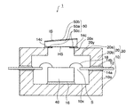
図3に示すように、本発明の第1実施形態の電子部品装置1のパッケージ本体30は、下側パッケージ部10とリング状の上側パッケージ部20とによって構成されている。下側パッケージ部10では、中央主要部に凹部10xを備えることで周縁部に突出部10aが設けられている。さらに、下側パッケージ部10の凹部10xの底面に光スイッチ素子40(電子部品)が接着剤16によって固着されている。光スイッチ素子40は、シリコン基板の上に数μm角のミラーが多数並べて構成されるプロジェクタの光学素子であり、光源からの光を反射させてスクリーンに画像を投影する機能を有する。なお、本実施形態では、電子部品として光スイッチ素子40を例示するが、EEPROMなどのメモリ素子、各種のMEMS(Micro Electro Mechanical Systems)素子、撮像素子(CCDやCMOSセンサ)などの外部からの光を受光する電子部品を実装してもよい。
As shown in FIG. 3, the
下側パッケージ部10の突出部10aの上面にはその内部から外部に延在する複数のリード12が融点ガラス14aによって固着された状態で並列して配置されている、さらに、光スイッチ素子40がワイヤ18によって内部のリード12に電気接続されている。
A plurality of
また、上側パッケージ部20は、中央部に開口部20xが設けられた上側枠部20aと、その周縁下部に繋がって設けられた立設枠部20bとによって構成されており、内部に凹部20yを備えている。上側パッケージ部20の開口部20xは光スイッチ素子40に対応する大きさに設定されている。下側、上側パッケージ部10,20は、セラミック、金属、半導体(シリコンなど)、又は樹脂などから形成される。
The
そして、上側パッケージ部20の凹部20yが下側パッケージ部10の凹部10xに対向するように、上側パッケージ部20の立設枠部20bが下側パッケージ部10の突出部10a上にリード12を挟むようにして低融点ガラス14bによって固着されている。上側パッケージ部20の上側枠部20aの外面は、光スイッチ素子40の受光面と平行な水平面となって配置される。
Then, the standing
さらに、上側パッケージ部20の開口部20xを塞ぐように、光透過窓部50が上側パッケージ部20の外面側における開口部20xの近傍部に低融点ガラス14cによって固着されている。
Furthermore, the light
このようにして、光スイッチ素子40は、下側、上側パッケージ部10,20の各凹部10x、20yによって構成される収容部Sに収容されていると共に、上側パッケージ部20の開口部20xを塞ぐ光透過窓部50によって気密封止された状態で実装されている。
In this way, the
図3に例示された光透過窓部50は、上面及び下面が鏡面となった透明ガラス50aの上面(傾斜面IS)側に反射防止層(ARコート)50bが形成され、下面(水平面HS)側にクロム(Cr)などからなる遮光膜パターン50cが形成されて構成されている。遮光膜パターン50cは、上側パッケージ部20の開口部20x内の透明ガラス50aの下面周縁部にリング状に形成されており、遮光膜パターン50cから内側が光透過領域となっている。なお、光透過窓部50の材料としては、透明ガラス50a以外の透光性部材を使用してもよい。また、反射防止層50b及び遮光膜パターン50cを省略してもよいし、反射防止層50bの代わりに反射防止機能をもたない保護膜を形成するようにしてもよい。
The
また、光透過窓部50の光透過方向の一対の対向面のうち、上面は光スイッチ素子40の受光面(実装面)に対して3°程度の角度で傾斜する傾斜面ISとなっており、下面は光スイッチ素子40の受光面と平行である水平面HSとなっている。そして、光透過窓部50の水平面HSが上側パッケージ部20の外面側の開口部20xの近傍部(光スイッチ素子40の受光面と平行面)に低融点ガラス14cによって固着されている。これにより、光透過窓部50の上面は光スイッチ素子40の受光面に対して3°程度の角度で傾斜する傾斜面ISとなって配置されている。
Of the pair of opposing surfaces in the light transmission direction of the
このように、本実施形態の電子部品装置1では、光透過窓部50自体に傾斜面ISを高精度で形成しておき、光透過窓部50の水平面HSを上側パッケージ部20の開口部20xの近傍部に固着するようにしている。このため、上側パッケージ部20の開口部20x内に高さの異なる段差を形成して光透過窓部を配置する方法(図2)と違って、上側パッケージ部20を寸法精度の悪いセラミックから形成する場合であってもセラミックの寸法精度は光透過窓部50の傾斜には影響しないので、光透過窓部50はその傾斜面ISの傾斜角度がずれることなくパッケージ本体に配置される。
Thus, in the
本実施形態の電子部品装置1の光透過窓部50を採用することにより、図2で説明した構造とする場合よりも光透過窓50の傾斜面ISの傾斜角度の精度を格段に向上させることができる。
By adopting the light
本実施形態の電子部品装置では、光源からの光が光透過窓部50を透過した後に光スイッチ素子40で反射され、その反射光が光透過窓部50を透過して外部のスクリーンに投影されて画像が得られる。本実施形態では、光透過窓部50はその上面が所望の傾斜角度(例えば3°程度)をもった傾斜面ISとなっていることから、光透過窓部50の表面での反射光は投影画像以外の領域に反射されるので、投影画像のコントラスト比を高くすることができ、表示特性の向上を図ることができる。
In the electronic component device of the present embodiment, light from the light source passes through the light
また、光透過窓部50の周縁部には遮光膜パターン50cが形成されているので、光スイッチ素子40からの反射光のうち光透過窓部50の周縁側での不必要な光反射が抑制され、光透過窓部50の所望の光透過部を透過した必要な反射光のみが外部に放出される。
Further, since the light-shielding
本実施形態の電子部品装置1の製造方法は、まず、上記した図3に示すような中央主要部に凹部10xを備えることで周縁部に突出部10aが形成された下側パッケージ部10を作成する。例えば、金型でセラミック粉末を成形し、その粉末成形体を焼結することにより下側パッケージ部10を得る。
In the manufacturing method of the
次いで、下側パッケージ部10の突出部10aの上面に低融点ガラス14aを介して複数のリード12を配置し、300〜400℃の温度で低融点ガラス14aを硬化させることにより、リード12を下側パッケージ部10の突出部10aに固着する。さらに、下側パッケージ部10の凹部10xの底面に接着剤16で光スイッチ素子40を固着した後に、ワイヤ18によって光スイッチ素子40とリード12とを電気接続する。
Next, a plurality of
続いて、下側パッケージ部10の作成方法と同様に、セラミックの粉末成形体を焼結するなどの方法により、上記した図3に示すような中央部に開口部20xを備えた上側枠部20aと立設枠部20bとにより構成される上側パッケージ部20を作成する。
Subsequently, the
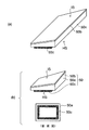
次に、上面に傾斜面ISをもつ光透過窓部50を作成する。まず、図4(a)及び(b)に示すように、上下面が水平面である短冊型の透明なガラス板50xを用意し、フライス盤、バフ研磨又はNCロータなどによりガラス板50xの上面全体を傾斜面ISに加工する。このとき、設計スペックを満足させる高い傾斜精度でガラス板50xに傾斜面ISを形成することができる。ガラス板50x以外にも透光性部材であれば使用することができる。
Next, the
次いで、図4(c)に示すように、ガラス板50xの傾斜面ISの上に反射防止膜50bを形成すると共に、ガラス板51の水平面HSにCr膜などの遮光膜51を形成する。その後に、図5(a)に示すように、遮光膜51をパターニングすることにより、個々の光透過窓部になる領域にリング状の遮光膜パターン50cを形成する。続いて、図5(b)に示すように、ガラス板50xを切断することにより、個々の光透過窓部50を得る。
Next, as shown in FIG. 4C, an
本実施形態の光透過窓部50では、短冊型のガラス板50xの上面全体に高精度に傾斜角が制御された傾斜面ISを形成した後に、それを切断することによって複数個得ることができるので、所望の傾斜面を有する光透過窓部50を低コストで作成することができる。なお、個片化されたガラス部材に反射防止膜50bや遮光膜パターン50cを形成して作成しても差し支えない。
In the light
続いて、上側パッケージ部20の開口部20xの外面近傍部に、光透過窓部50の遮光膜パターン50cから外側部分を低融点ガラス14cによって固着して開口部20xを塞ぐ。その後に、光透過窓部50が取り付けられた上側パッケージ部20の立設枠部20bを下側パッケージ部10の突出部10aに低融点ガラス14bによって固着することにより、光スイッチ素子40を気密封止する。以上により、図3に示す本実施形態の電子部品装置1が得られる。
Subsequently, the outer portion of the
このように、本実施形態では、光スイッチ素子40の受光面に対して所望角度で傾斜する傾斜面をもつ光透過窓部50を備えた電子部品装置1を高歩留り及び低コストで製造することが可能になる。
As described above, in the present embodiment, the
なお、本実施形態では、パッケージ本体30が下側、上側パッケージ部10,20から構成されるようにしたが、下側、上側パッケージ部10,20が一体化された一体型のパッケージ本体を採用してもよい。この場合は、上部の開口部が電子部品を実装できてワイヤボンディング可能な大きさに設定され、側部に開口部を設けるなどしてリードを挿通して封止すればよい。
In the present embodiment, the
(第2の実施の形態)
図6は本発明の第2実施形態の電子部品装置を示す断面図である。図6に示すように、第2実施形態の電子部品装置1aでは、上側パッケージ部20の上側枠部20aの内面側における開口部20xの近傍部に光透過窓部50の水平面HSが低融点ガラス14cによって固着されて、光スイッチ素子40が収容部Sに気密封止されている。つまり、第2実施形態の光透過窓部50は、第1実施形態の光透過窓部50の配置が上下反転した状態で上側パッケージ部20の内面側に取り付けられており、光透過窓部50の傾斜面ISがパッケージ本体30の内面側に配置されている。
(Second Embodiment)
FIG. 6 is a sectional view showing an electronic component device according to the second embodiment of the present invention. As shown in FIG. 6, in the
上側パッケージ部20の上側枠部20aの内面は光スイッチ素子40の受光面と平行な水平面となっており、上側パッケージ部20の内面側に光透過窓部50の水平面HSを固着することにより、光透過窓部50は光スイッチ素子40の受光面に対して所望角度で傾斜する傾斜面ISをもって配置される。
The inner surface of the
光透過窓部50は、透明ガラス50aの上面(水平面HS)側に反射防止膜50bが形成され、下面(傾斜面IS)の周縁側に遮光膜パターン50cが形成されて構成されている。遮光膜パターン50cは、透明ガラス50aの下面周縁部から側面にかけてリング状に形成されている。なお、透明ガラス50aの側面を除く下面周縁部のみに遮光膜パターン50cを設けてもよい。
The
第2実施形態では、光透過窓部50以外の要素は第1実施形態と同一であるので、同一符号を付してその説明を省略する。
In 2nd Embodiment, since elements other than the light
第2実施形態では、第1実施形態と同様に光透過窓部50自体に傾斜面ISを設けるようにしたので、光スイッチ素子40の受光面に対して所望角度で傾斜する傾斜面ISをもつ光透過窓部50を精度よく取り付けることができる。これにより、第1実施形態と同様に、光透過窓部50での光反射による悪影響が抑制され、投影画像の表示特性を向上させることができる。
In the second embodiment, since the light
第2実施形態においても、下側、上側パッケージ10,20が一体化された一体型のパッケージ本体を採用してもよい。
Also in the second embodiment, an integrated package body in which the lower and
(第3の実施の形態)
図7は本発明の第3実施形態の電子部品装置を示す断面図である。図7に示すように、第3実施形態の電子部品装置1bは、第1実施形態の図3の上側パッケージ部20の上側枠部20aが省略された構成であり、上側パッケージ部20はリング状の立設枠部から構成され、内側が全て開口部20xとなっている。上側パッケージ部20の枠部上面は、光スイッチ素子40の受光面と平行な水平面となっている。そして、上側パッケージ部20に対応する大きさの光透過窓部50の水平面HSの周縁部が上側パッケージ部20の枠部上面に低融点ガラス14cによって固着されて、光スイッチ素子40が収容部Sに気密封止されている。
(Third embodiment)
FIG. 7 is a sectional view showing an electronic component device according to a third embodiment of the present invention. As shown in FIG. 7, the
これによって、光透過窓部50は光スイッチ素子40の受光面に対して所望の角度で傾斜する傾斜面ISをもってパッケージ本体30に配置される。光透過窓部50は、透明ガラス50aの上面(傾斜面IS)側に反射防止膜50bが形成され、下面(水平面HS)の周縁側に遮光膜パターン50cが形成されて構成されている。遮光膜パターン50cは、上側パッケージ部20の枠部の内面部から光スイッチ素子40の周縁部に対応する位置までリング状に形成され、遮光膜パターン50cの内側が光透過領域となっている。
Thus, the
第3実施形態では、上側パッケージ部20と光透過窓部50以外の要素は第1実施形態と同一であるので、同一符号を付してその説明を省略する。
In 3rd Embodiment, since elements other than the
第3実施形態は、第1実施形態と同様な効果を奏する。第3実施形態においても、下側、上側パッケージ部10,20が一体化された一体型のパッケージ本体を採用してもよい。
The third embodiment has the same effects as the first embodiment. Also in the third embodiment, an integrated package body in which the lower and
1,1a,1b…電子部品装置、10…下側パッケージ部、10x,20y…凹部、10a…突出部、12…リード、14a,14b,14c…低融点ガラス、16…接着剤、18…ワイヤ、20…上側パッケージ部、20a…上側枠部、20b…立設枠部、20x…開口部、30…パッケージ本体、40…光スイッチ素子(電子部品)、50…光透過窓部、50a…透明ガラス、50b…反射防止膜、50c…遮光膜パターン、50x…ガラス板、51…遮光膜、IS…傾斜面、HS…水平面、S…収容部。
DESCRIPTION OF
Claims (10)
前記パッケージ本体の前記収容部の底部に実装された電子部品と、
前記開口部を塞いで前記電子部品を気密封止し、外部からの光を前記電子部品に入射させるための光透過窓部とを有し、
前記光透過窓部は、光透過方向の一対の対向面が水平面と傾斜面の組み合わせから構成され、前記水平面が前記パッケージ本体の開口部の近傍部に固着されることによって、前記光透過窓部が前記電子部品の受光面に対して傾斜する前記傾斜面をもって配置されていることを特徴とする電子部品装置。 A package body provided with an accommodating portion inside and provided with an opening at the top;
An electronic component mounted on the bottom of the housing portion of the package body;
A light-transmitting window for closing the opening to hermetically seal the electronic component and allowing light from the outside to enter the electronic component;
The light transmission window portion includes a pair of opposed surfaces in the light transmission direction configured by a combination of a horizontal surface and an inclined surface, and the light transmission window portion is fixed to the vicinity of the opening of the package body. Is arranged with the inclined surface inclined with respect to the light receiving surface of the electronic component.
中央主要部に凹部を備えて周縁部に突出部が設けられた下側パッケージ部の上に、中央部に前記開口部が設けられた上側枠部と該上側枠部の周縁下部に繋がる立設枠部とから形成された上側パッケージ部が配置されて構成されていることを特徴とする請求項1に記載の電子部品装置。 The package body is
On the lower package part provided with a recess in the central main part and provided with a protruding part on the peripheral part, an upper frame part provided with the opening part in the central part and a standing part connected to the lower peripheral part of the upper frame part The electronic component device according to claim 1, wherein an upper package portion formed of a frame portion is arranged.
中央主要部に凹部を備えて周縁部に突出部が設けられた下側パッケージ部の上に、内側全体が前記開口部となった立設枠部からなる上側パッケージ部が配置されて構成されていることを特徴とする請求項1に記載の電子部品装置。 The package body is
On the lower package part provided with a recess in the central main part and provided with a projecting part at the peripheral part, an upper package part composed of a standing frame part in which the entire inside becomes the opening part is arranged and configured. The electronic component device according to claim 1, wherein:
前記透明ガラスの下面の周縁側に遮光膜パターンが形成されていることを特徴とする請求項7に記載の電子部品装置。 An antireflection film or a protective film is formed on the upper surface of the transparent glass,
The electronic component device according to claim 7, wherein a light shielding film pattern is formed on a peripheral side of the lower surface of the transparent glass.
Priority Applications (1)
| Application Number | Priority Date | Filing Date | Title |
|---|---|---|---|
| JP2006102213A JP2007281021A (en) | 2006-04-03 | 2006-04-03 | Electronic component device |
Applications Claiming Priority (1)
| Application Number | Priority Date | Filing Date | Title |
|---|---|---|---|
| JP2006102213A JP2007281021A (en) | 2006-04-03 | 2006-04-03 | Electronic component device |
Publications (2)
| Publication Number | Publication Date |
|---|---|
| JP2007281021A true JP2007281021A (en) | 2007-10-25 |
| JP2007281021A5 JP2007281021A5 (en) | 2009-03-26 |
Family
ID=38682196
Family Applications (1)
| Application Number | Title | Priority Date | Filing Date |
|---|---|---|---|
| JP2006102213A Pending JP2007281021A (en) | 2006-04-03 | 2006-04-03 | Electronic component device |
Country Status (1)
| Country | Link |
|---|---|
| JP (1) | JP2007281021A (en) |
Cited By (3)
| Publication number | Priority date | Publication date | Assignee | Title |
|---|---|---|---|---|
| WO2009057602A1 (en) | 2007-10-29 | 2009-05-07 | Ntt Docomo, Inc. | Mobile communication system, home base station, and mobile station |
| JP2016184069A (en) * | 2015-03-26 | 2016-10-20 | セイコーエプソン株式会社 | Electro-optic device, method for manufacturing electro-optic device, and electronic apparatus |
| JP2018064081A (en) * | 2016-10-07 | 2018-04-19 | 日本電気硝子株式会社 | Airtight package and method for manufacturing the same |
Citations (8)
| Publication number | Priority date | Publication date | Assignee | Title |
|---|---|---|---|---|
| JPS63149553A (en) * | 1986-12-12 | 1988-06-22 | Nippon Mining Co Ltd | Electronic hygrometer |
| JPH0338884A (en) * | 1989-07-06 | 1991-02-19 | Fuji Electric Co Ltd | Light shielding structure for semiconductor device |
| JPH03188680A (en) * | 1989-12-18 | 1991-08-16 | Toshiba Corp | Solid image pick-up device |
| JP2001345391A (en) * | 2000-03-28 | 2001-12-14 | Canon Inc | Electronic component and its manufacturing method |
| JP2004505267A (en) * | 2000-07-28 | 2004-02-19 | 大塚電子株式会社 | Spectral light detector |
| JP2004134721A (en) * | 2002-10-09 | 2004-04-30 | Optware:Kk | Photodetector, optical information reproducing apparatus provided with it, optical information recording and reproducing apparatus |
| JP2005518673A (en) * | 2002-02-25 | 2005-06-23 | シリコン バンドウィドス インコーポレイテッド | Module type semiconductor die package and manufacturing method thereof |
| JP2007165464A (en) * | 2005-12-12 | 2007-06-28 | Stanley Electric Co Ltd | Semiconductor optical device |
-
2006
- 2006-04-03 JP JP2006102213A patent/JP2007281021A/en active Pending
Patent Citations (8)
| Publication number | Priority date | Publication date | Assignee | Title |
|---|---|---|---|---|
| JPS63149553A (en) * | 1986-12-12 | 1988-06-22 | Nippon Mining Co Ltd | Electronic hygrometer |
| JPH0338884A (en) * | 1989-07-06 | 1991-02-19 | Fuji Electric Co Ltd | Light shielding structure for semiconductor device |
| JPH03188680A (en) * | 1989-12-18 | 1991-08-16 | Toshiba Corp | Solid image pick-up device |
| JP2001345391A (en) * | 2000-03-28 | 2001-12-14 | Canon Inc | Electronic component and its manufacturing method |
| JP2004505267A (en) * | 2000-07-28 | 2004-02-19 | 大塚電子株式会社 | Spectral light detector |
| JP2005518673A (en) * | 2002-02-25 | 2005-06-23 | シリコン バンドウィドス インコーポレイテッド | Module type semiconductor die package and manufacturing method thereof |
| JP2004134721A (en) * | 2002-10-09 | 2004-04-30 | Optware:Kk | Photodetector, optical information reproducing apparatus provided with it, optical information recording and reproducing apparatus |
| JP2007165464A (en) * | 2005-12-12 | 2007-06-28 | Stanley Electric Co Ltd | Semiconductor optical device |
Cited By (4)
| Publication number | Priority date | Publication date | Assignee | Title |
|---|---|---|---|---|
| WO2009057602A1 (en) | 2007-10-29 | 2009-05-07 | Ntt Docomo, Inc. | Mobile communication system, home base station, and mobile station |
| JP2016184069A (en) * | 2015-03-26 | 2016-10-20 | セイコーエプソン株式会社 | Electro-optic device, method for manufacturing electro-optic device, and electronic apparatus |
| US10739554B2 (en) | 2015-03-26 | 2020-08-11 | Seiko Epson Corporation | Electro-optical device, manufacturing method of electro-optical device, and electronic apparatus |
| JP2018064081A (en) * | 2016-10-07 | 2018-04-19 | 日本電気硝子株式会社 | Airtight package and method for manufacturing the same |
Similar Documents
| Publication | Publication Date | Title |
|---|---|---|
| TWI735232B (en) | Light emitter and light detector modules and method of fabricating the same | |
| US7030926B2 (en) | Image pick-up apparatus and portable telephone utilizing the same | |
| WO2019076352A1 (en) | Photosensitive assembly based on metal support, and camera module | |
| US20140355095A1 (en) | Multi-purpose optical cap and apparatus and methods useful in conjunction therewith | |
| JP2007287967A (en) | Electronic-component apparatus | |
| JP2007142042A (en) | Semiconductor package, manufacturing method thereof, semiconductor module, and electronic equipment | |
| JPWO2007083579A1 (en) | Compound eye camera module and manufacturing method thereof | |
| US8056247B2 (en) | Tilt sensor | |
| JPWO2006046396A1 (en) | The camera module | |
| TWI847881B (en) | Method of manufacturing light emitting module, light emitting module, and projector | |
| TW201417250A (en) | Optical module, in particular opto-electronic module, and method of manufacturing the same | |
| JP2002350608A (en) | Image pickup lens, image pickup device, metallic mold and method for molding image pickup lens | |
| JP4248586B2 (en) | IMAGING DEVICE, MANUFACTURING METHOD THEREOF, AND PORTABLE INFORMATION TERMINAL AND IMAGING DEVICE WITH THE IMAGING DEVICE | |
| WO2018219358A1 (en) | Optical lens, optical component and optical module and manufacturing method | |
| CN106660781B (en) | For the assembly of micromirror chip, mirroring apparatus and for the manufacturing method of mirroring apparatus | |
| JP2006269841A (en) | Solid-state imaging device | |
| JP2007281021A (en) | Electronic component device | |
| JP6992163B2 (en) | Manufacturing methods and molds for photosensitive assemblies, imaging modules, smart terminals and photosensitive assemblies | |
| JP2017032875A (en) | Optical device | |
| JP6529431B2 (en) | Optical element package | |
| JP2014186136A (en) | Semiconductor device having mirror surface | |
| TW201518777A (en) | Lens array, lens array stack, and method for fabrication thereof | |
| JP2005217337A (en) | Optical device | |
| JP2004266844A (en) | Imaging unit and manufacturing method thereof | |
| JP4277665B2 (en) | Imaging device and portable terminal equipped with the imaging device |
Legal Events
| Date | Code | Title | Description |
|---|---|---|---|
| A521 | Request for written amendment filed |
Free format text: JAPANESE INTERMEDIATE CODE: A523 Effective date: 20090204 |
|
| A621 | Written request for application examination |
Free format text: JAPANESE INTERMEDIATE CODE: A621 Effective date: 20090204 |
|
| A977 | Report on retrieval |
Free format text: JAPANESE INTERMEDIATE CODE: A971007 Effective date: 20090910 |
|
| A131 | Notification of reasons for refusal |
Free format text: JAPANESE INTERMEDIATE CODE: A131 Effective date: 20110913 |
|
| A02 | Decision of refusal |
Free format text: JAPANESE INTERMEDIATE CODE: A02 Effective date: 20120131 |