JP2007272122A - Optical control element - Google Patents
Optical control element Download PDFInfo
- Publication number
- JP2007272122A JP2007272122A JP2006100527A JP2006100527A JP2007272122A JP 2007272122 A JP2007272122 A JP 2007272122A JP 2006100527 A JP2006100527 A JP 2006100527A JP 2006100527 A JP2006100527 A JP 2006100527A JP 2007272122 A JP2007272122 A JP 2007272122A
- Authority
- JP
- Japan
- Prior art keywords
- control element
- light control
- electrode
- transparent conductive
- conductive film
- Prior art date
- Legal status (The legal status is an assumption and is not a legal conclusion. Google has not performed a legal analysis and makes no representation as to the accuracy of the status listed.)
- Pending
Links
Images


Landscapes
- Optical Modulation, Optical Deflection, Nonlinear Optics, Optical Demodulation, Optical Logic Elements (AREA)
Abstract
Description
本発明は、光制御素子に関し、特に、電気光学効果を有する結晶性基板に光導波路と変調電極とを形成した光制御素子に関する。 The present invention relates to a light control element, and more particularly to a light control element in which an optical waveguide and a modulation electrode are formed on a crystalline substrate having an electro-optic effect.
従来、光通信分野や光測定分野において、電気光学効果を有する基板上に光導波路や変調電極を形成した導波路型光変調器などの光制御素子が多用されている。
LiNbO3などの電気光学効果を有する基板を用いた光導波路型光スイッチや光変調器は、光路をスイッチするあるいは変調するための制御信号(変調信号)が印加される電極には、金属が用いられるのが一般的である。
Conventionally, in the optical communication field and the optical measurement field, a light control element such as a waveguide type light modulator in which an optical waveguide or a modulation electrode is formed on a substrate having an electro-optic effect is widely used.
In an optical waveguide type optical switch or optical modulator using a substrate having an electro-optic effect such as LiNbO 3 , a metal is used for an electrode to which a control signal (modulation signal) for switching or modulating an optical path is applied. It is common that
光制御素子の電極に金属膜を用い、しかも該光制御素子をTMモードで動作させる場合には、金属膜による光の吸収を防ぐために、光導波路と金属膜との間に、LiNbO3基板よりも屈折率が低く、光の吸収の少ないバッファ層を施す必要がある。このバッファ層は通常SiO2、Si3N4、SiONなどが用いられる。
また、光変調周波数の広帯域化や低駆動電圧化などを実現するために、光導波路をドライエッチングを用いてリッジ型構造とするなど、これまでに様々な方法が提案されている。
When a metal film is used as the electrode of the light control element and the light control element is operated in the TM mode, a LiNbO 3 substrate is interposed between the optical waveguide and the metal film in order to prevent light absorption by the metal film. However, it is necessary to provide a buffer layer having a low refractive index and low light absorption. The buffer layer such as an ordinary SiO 2, Si 3 N 4, SiON is used.
In addition, various methods have been proposed so far, such as making the optical waveguide into a ridge structure by using dry etching in order to realize a wide band of the optical modulation frequency and a low driving voltage.
以下の特許文献1又は2においては、制御信号が印加される電極として、基板よりも屈折率が低い導電膜を直接に基板上に形成し、かつ、光導波路上の導電膜領域を除く領域には金属膜を設けた光デバイスが提案されている。特に、これらの文献では、基板よりも屈折率が低い導電膜として、ITO(In2O3−SnO2)や有機導電性材料が例示され、金属膜と組み合わせて、高速動作を可能とする光制御素子が開示されている。
しかしながら、上述した特許文献1又は2においては、実デバイスとしての使用を考えた際に大きな問題点が存在する。すなわち、通信波長帯で使用される光制御素子にITO材料を導電性材料として用いると挿入損失が大きく、実デバイスとして使用できない挿入損失レベルとなる。この原因は、ITOは可視領域においては透過特性に優れる(透過率が80%以上)ものの、1200nm以上の波長域では、透過率はほぼゼロとなることによるものであることが明らかとなった。
また、有機導電性材料の場合には、光制御素子の製造過程で熱処理を行うため、熱処理温度など製造上の制限が厳しく、しかも、実デバイスとしての長期信頼性にも不安がある。
However, in
In the case of an organic conductive material, heat treatment is performed in the manufacturing process of the light control element, so that there are severe restrictions on the production such as the heat treatment temperature, and there is a concern about long-term reliability as an actual device.
さらに、以下の特許文献3には、赤外透過率の高い酸化インジウム系の酸化物透明電極としてチタンやタングステンを含有する材料が開示されている。特許文献3においては、酸化物透明電極の用途として、赤外域における太陽電池への適用や光検出素子への適用が例示されているが、光制御素子の電極のように、光の屈折率を制御する機能を持つ、パターン制御された電極として用いる方法については、何ら開示されておらず、後述する新規の構造を有する光制御素子に使用する示唆もない。
他方、以下の特許文献4又は5においては、30μm以下の厚みを有する極めて薄い基板(以下、「第1基板」という。)に、光導波路並びに変調電極を組み込み、第1基板より誘電率の低い他の基板を接合し、マイクロ波に対する実効屈折率を下げ、マイクロ波と光波との速度整合を図ることが行われている。
特許文献4又は5においては、薄板化された第1基板を用いることで、光制御素子の設計自由度が飛躍的に高まり、例えばバッファ層を用いずとも、低駆動電圧の光変調器などが作製可能となることが開示されている。しかしながら、バッファ層を用いない構造においても、変調電極となる金属電極を、導波路近傍の所定範囲以内に配置すると、光波の吸収が生じ挿入損失が増大する問題が知られている。
In
本発明が解決しようとする課題は、上述したような問題を解決し、従来よりも挿入損失を抑制し、かつ低駆動電圧で動作可能な光制御素子を提供することである。 The problem to be solved by the present invention is to solve the above-described problems, to provide an optical control element that can operate at a low drive voltage, with a lower insertion loss than in the prior art.
上記課題を解決するため、請求項1に係る発明では、電気光学効果を有する結晶基板と、該基板に形成された光導波路と、該光導波路を通過する光を変調するための変調電極とを有する光制御素子において、該変調電極を構成する信号電極と接地電極のうち、少なくとも一方にはTiとInの複合酸化物からなる赤外透明導電膜が用いられることを特徴とする。
なお、本発明における「赤外透明導電膜」とは、波長領域が1200nm以上の領域において、透過率が80%以上、好ましくは95%以上であり、かつ、体積抵抗値が5×101Ωcmよりも小さいものを意味する。
In order to solve the above-described problem, in the invention according to
The “infrared transparent conductive film” in the present invention means that the transmittance is 80% or more, preferably 95% or more, and the volume resistance value is 5 × 10 1 Ωcm in the wavelength region of 1200 nm or more. Means something smaller.
請求項2に係る発明では、請求項1に記載の光制御素子において、該信号電極と該接地電極の少なくとも一方が、該赤外透明導電膜と金属膜とからなる2層以上の構造を有していることを特徴とする。
In the invention according to
請求項3に係る発明では、請求項2に記載の光制御素子において、該信号電極及び該接地電極が共に、赤外透明導電膜と金属膜とから構成され、該信号電極の金属膜と該接地電極の金属膜との最小間隔が15μm以下であることを特徴とする。
In the invention according to
請求項4に係る発明では、請求項1乃至3のいずれかに記載の光制御素子において、該光導波路がリッジ型光導波路からなることを特徴とする。 According to a fourth aspect of the present invention, in the light control element according to any one of the first to third aspects, the optical waveguide is a ridge type optical waveguide.
請求項5に係る発明では、請求項1乃至4のいずれかに記載の光制御素子において、該結晶基板の厚みが10μm以下であることを特徴とする。
The invention according to
請求項6に係る発明では、請求項5に記載の光制御素子において、該信号電極が形成された結晶基板の面と異なる面に、赤外透明導電膜を有する接地電極が形成されていることを特徴とする。
In the invention according to claim 6, in the light control element according to
請求項7に係る発明では、請求項1乃至6のいずれかに記載の光制御素子において、該光導波路が分岐又は合波する2つの分岐導波路を有し、分岐導波路に変調電極が電界を印加させる領域における該結晶基板の自発分極の向きが、各分岐導波路毎に異なることを特徴とする。 According to a seventh aspect of the present invention, in the light control element according to any one of the first to sixth aspects, the optical waveguide has two branch waveguides that branch or multiplex, and the modulation electrode is provided in the branch waveguide. The direction of spontaneous polarization of the crystal substrate in the region to which is applied is different for each branching waveguide.
請求項8に係る発明では、請求項1乃至7のいずれかに記載の光制御素子において、該赤外透明導電膜と該結晶基板との間に、1μm以下の厚みを有するバッファ層が形成されていることを特徴とする。
In the invention according to claim 8, in the light control element according to any one of
請求項9に係る発明では、請求項1乃至8のいずれかに記載の光制御素子において、該赤外透明導電膜は、In酸化物を母体とし、Ti酸化物が0.3から1.5wt%の範囲で含有されていることを特徴とする。 According to a ninth aspect of the present invention, in the light control element according to any one of the first to eighth aspects, the infrared transparent conductive film includes an In oxide as a base and a Ti oxide of 0.3 to 1.5 wt. % Content.
請求項10に係る発明では、請求項1乃至9のいずれかに記載の光制御素子において、該赤外透明導電性膜は、スパッタリング法により形成された後、抵抗値と透過率を調整するための熱処理工程を経ることを特徴とする。 According to a tenth aspect of the present invention, in the light control element according to any one of the first to ninth aspects, the infrared transparent conductive film is formed by a sputtering method, and then adjusts a resistance value and a transmittance. The heat treatment process is performed.
請求項11に係る発明では、請求項1乃至10のいずれかに記載の光制御素子において、該光制御素子は光通信波長帯よりも波長の長い領域にて使用されることを特徴とする。 According to an eleventh aspect of the present invention, in the light control element according to any one of the first to tenth aspects, the light control element is used in a region having a longer wavelength than the optical communication wavelength band.
請求項1に係る発明により、信号電極と接地電極のうち、少なくとも一方にはTiとInの複合酸化物からなる赤外透明導電膜を用いるため、光制御素子の使用波長が1200nmを超えても光の吸収が生じず、バッファ層が不要もしくは厚みを低減できることから、挿入損失の増大なしに、低駆動電圧デバイスが提供できる。さらに、赤外透明電極膜は、金属電極に比べ光の吸収が極めて小さいことから、従来よりも光導波路の近傍に変調電極を配置できる。すなわち、電界がより効果的に光導波路へ印加される相乗効果により、さらなる低駆動電圧の光制御素子を提供することが可能となる。 According to the first aspect of the present invention, an infrared transparent conductive film made of a composite oxide of Ti and In is used for at least one of the signal electrode and the ground electrode, so that even if the wavelength used for the light control element exceeds 1200 nm, Absorption of light does not occur and a buffer layer is unnecessary or the thickness can be reduced, so that a low drive voltage device can be provided without an increase in insertion loss. Furthermore, since the infrared transparent electrode film absorbs light much less than the metal electrode, the modulation electrode can be disposed near the optical waveguide as compared with the conventional case. That is, it is possible to provide a light control element with a further low driving voltage due to a synergistic effect in which the electric field is applied to the optical waveguide more effectively.
請求項2に係る発明により、信号電極と接地電極の少なくとも一方が赤外透明導電膜と金属膜とからなる2層以上の構造を有しているため、電極自体の抵抗値を、赤外透明導電膜のみの場合よりも小さくでき、高周波領域においても高速動作を可能とする光制御素子を提供することが可能となる。 According to the second aspect of the present invention, since at least one of the signal electrode and the ground electrode has a structure of two or more layers including an infrared transparent conductive film and a metal film, the resistance value of the electrode itself is reduced to infrared transparent. It is possible to provide a light control element that can be made smaller than the case of using only a conductive film and that can operate at high speed even in a high-frequency region.
請求項3に係る発明により、信号電極及び接地電極が共に、赤外透明導電膜と金属膜とから構成されているため、該信号電極の金属膜と該接地電極の金属膜との最小間隔を15μm以下とすることも可能となり、より一層の低駆動電圧の光制御素子を提供することが可能となる。
According to the invention of
請求項4に係る発明により、光導波路がリッジ型光導波路からなるため、光の閉じ込めの大きな導波路を利用でき、従来と比較して導波路間隔の縮小が図れる効果とともに、赤外透明導電膜が金属膜よりも導波路に近接して配置できる相乗効果から、さらなる低駆動電圧型の光制御素子を提供することが可能となる。また、赤外透明導電膜であれば、光波の吸収なしにリッジ型導波路の側面を含む領域において電極を形成することできるため、さらなる低駆動電圧化への効果がある。
According to the invention of
請求項5に係る発明により、結晶基板の厚みが10μm以下であるため、設計の自由度が広まることから、例えば、赤外透明導電膜を従来よりも導波路に近接配置した場合においても、インピーダンスや速度整合条件を満たす構造が得られるなど、信号電極と接地電極の配置上の制約が小さくなるとともに、基板の有効利用が可能になるため、より効率的に低駆動電圧型の光制御素子を提供することが可能となる。
According to the invention of
請求項6に係る発明により、信号電極が形成された結晶基板の面と異なる面に、赤外透明導電膜を有する接地電極が形成されているため、基板の有効利用が可能になるとともに、作製再現性の向上を図ることが可能となる。しかも、結晶基板の厚みが10μm以下の場合には、結晶基板を挟んで配置された信号電極及び接地電極により、光導波路に電界をより効果的に印加することが可能となるため、より低駆動電圧型の光制御素子を提供することが可能となる。 According to the invention of claim 6, since the ground electrode having the infrared transparent conductive film is formed on a surface different from the surface of the crystal substrate on which the signal electrode is formed, the substrate can be effectively used and manufactured. It becomes possible to improve the reproducibility. In addition, when the thickness of the crystal substrate is 10 μm or less, an electric field can be more effectively applied to the optical waveguide by the signal electrode and the ground electrode arranged with the crystal substrate interposed therebetween. A voltage type light control element can be provided.
請求項7に係る発明により、光導波路が分岐又は合波する2つの分岐導波路を有し、分岐導波路に変調電極が電界を印加させる領域における該結晶基板の自発分極の向きが、各分岐導波路毎に異なるため、外部電気デバイスを用いることなく容易に差動駆動が可能となり、より低駆動電圧での動作が可能な光制御素子を提供することが可能となる。 According to the invention of claim 7, the optical waveguide has two branch waveguides that branch or multiplex, and the direction of the spontaneous polarization of the crystal substrate in the region where the modulation electrode applies an electric field to the branch waveguides Since each waveguide is different, differential driving can be easily performed without using an external electric device, and a light control element capable of operating at a lower driving voltage can be provided.
請求項8に係る発明により、赤外透明導電膜と結晶基板との間に、1μm以下の厚みを有するバッファ層が形成されているため、低駆動電圧を損なうことなく、光波の吸収をより厳密に抑制し、かつ、速度整合条件を緩和することが可能となる。 According to the eighth aspect of the present invention, since the buffer layer having a thickness of 1 μm or less is formed between the infrared transparent conductive film and the crystal substrate, light wave absorption is more strictly performed without impairing the low driving voltage. And the speed matching condition can be relaxed.
請求項9に係る発明により、赤外透明導電膜はIn酸化物を母体とし、Ti酸化物が0.3から1.5wt%の範囲であるため、キャリア濃度が適当であり高透過率かつ低体積抵抗値を両立した赤外透明導電膜を形成でき、挿入損失が抑制され、かつ低駆動電圧で動作可能な光制御素子を提供することが可能となる。 According to the invention of claim 9, since the infrared transparent conductive film is based on In oxide and Ti oxide is in the range of 0.3 to 1.5 wt%, the carrier concentration is appropriate, high transmittance and low It is possible to provide an optical control element that can form an infrared transparent conductive film having both volume resistance values, can suppress insertion loss, and can operate at a low driving voltage.
請求項10に係る発明により、赤外透明導電性膜はスパッタリング法により作製された後、抵抗値と透過率を調整するための熱処理工程を経るため、原材料と成膜試料の組成ずれが少なく、プロセスマージンを広く取ることが出来る。また、熱処理により透過率と体積抵抗値を後工程において調整できることから、歩留まりよく低駆動電圧型の光制御素子を提供することが可能となる。
According to the invention of
請求項11に係る発明により、光制御素子は光通信波長帯よりも波長の長い領域にて使用されるため、光通信波長デバイスとしては特に挿入損失の小さい光制御素子を提供することが可能となる。
According to the invention of
以下、本発明を好適例を用いて詳細に説明する。
本発明は、図1乃至8に示すように、電気光学効果を有する結晶基板(1,1’)と、該基板に形成された光導波路(2,2’)と、該光導波路を通過する光を変調するための変調電極とを有する光制御素子において、該変調電極を構成する信号電極3と接地電極(4,5)のうち、少なくとも一方にはTiとInの複合酸化物からなる赤外透明導電膜12が用いられることを特徴とする。
Hereinafter, the present invention will be described in detail using preferred examples.
As shown in FIGS. 1 to 8, the present invention passes through a crystal substrate (1, 1 ′) having an electro-optic effect, an optical waveguide (2, 2 ′) formed on the substrate, and the optical waveguide. In a light control element having a modulation electrode for modulating light, at least one of the
電気光学効果を有する結晶性基板としては、例えば、ニオブ酸リチウム、タンタル酸リチウム、PLZT(ジルコン酸チタン酸鉛ランタン)、及び石英系の材料及びこれらの組み合わせが利用可能である。特に、電気光学効果の高いニオブ酸リチウム(LN)やタンタル酸リチウム(LT)結晶が好適に利用される。また、結晶性基板として、Xカット型の基板を使用した場合には、結晶基板の表面に平行な方向に対して光導波路を挟むように変調電極が配置され、Zカット型の場合にはバッファ層を介して、光導波路の直上に変調電極が配置されることが一般的である。ただし、Zカット型で、分極反転を利用した構造の場合には、例えば、マッハツェンダー型の光導波路の中央に信号電極を配することでプッシュプル動作が可能となる。この場合は必ずしもバッファ層を必要としない。 As a crystalline substrate having an electro-optic effect, for example, lithium niobate, lithium tantalate, PLZT (lead lanthanum zirconate titanate), quartz-based materials, and combinations thereof can be used. In particular, lithium niobate (LN) or lithium tantalate (LT) crystals having a high electro-optic effect are preferably used. In addition, when an X-cut substrate is used as the crystalline substrate, the modulation electrode is disposed so as to sandwich the optical waveguide in a direction parallel to the surface of the crystal substrate. In general, a modulation electrode is disposed directly on an optical waveguide via a layer. However, in the case of a Z-cut type structure using polarization inversion, for example, a push-pull operation can be performed by arranging a signal electrode in the center of a Mach-Zehnder type optical waveguide. In this case, the buffer layer is not necessarily required.
変調電極は、信号電極、接地電極又はDC電極など光制御素子を駆動するために、結晶性基板上に形成される種々の電極を含むものである。赤外透明導電膜を変調電極として形成するには、フォトリソグラフィー法により電極パターンを形成しリフトオフ法によって形成する方法や、所定の電極パターンが残るようにマスク材を形成し、ドライエッチング、あるいはウエットエッチングにて形成する方法などことが可能である The modulation electrode includes various electrodes formed on the crystalline substrate in order to drive a light control element such as a signal electrode, a ground electrode, or a DC electrode. In order to form an infrared transparent conductive film as a modulation electrode, an electrode pattern is formed by a photolithography method and formed by a lift-off method, a mask material is formed so that a predetermined electrode pattern remains, dry etching, or wet It is possible to form by etching
赤外透明導電膜としては、InとTiの複合酸化物膜を用いる。これは波長1200nm以上の領域においても高透過率を示すためである。通信波長帯用の光制御素子、例えば1550nmにおいて使用される光制御素子の場合には、赤外透明導電膜の1550nmにおける透過率が80%以上であることが望ましく、さらには95%以上の透過率がより好ましい。体積抵抗値は小さいほど好ましく、InとTiの複合酸化物膜の場合にはその値は1×10⁻⁴Ωcm程度が期待できる。ただし、これら光制御素子を低周波数領域(おおむね1GHz以下)にて使用する場合や、赤外透明導電膜を接地電極として使用する場合には体積抵抗値の制限は小さく、接地電極としては5×101Ωcm程度でも十分である。 A composite oxide film of In and Ti is used as the infrared transparent conductive film. This is because high transmittance is exhibited even in a wavelength region of 1200 nm or more. In the case of a light control element for a communication wavelength band, for example, a light control element used at 1550 nm, the transmittance of the infrared transparent conductive film at 1550 nm is preferably 80% or more, and more preferably 95% or more. The rate is more preferred. The smaller the volume resistance value, the better. In the case of a composite oxide film of In and Ti, the value can be expected to be about 1 × 10 −4 Ωcm. However, when these light control elements are used in a low frequency region (generally 1 GHz or less), or when an infrared transparent conductive film is used as a ground electrode, the volume resistance value is less limited. Even about 10 1 Ωcm is sufficient.
赤外透明導電膜は、その作製条件によりその物性値が大きく異なる。表1には作製時に供給した酸素分圧の違いによる、透過率と体積抵抗値を示した。表1における赤外透明導電膜の共通作製条件はDCパワー300W、スパッタガスAr+O2であり、膜厚は200nmに設定した。
透過率は分光光度計U4000(日立製作所製)を用いて測定した。表中には試験光が1550nmの場合の値を記した。
体積抵抗値は抵抗測定器(ダイヤインスツルメンツ製、MCP−T610型)による4探針法を用いて測定した。
Infrared transparent conductive films vary greatly in physical properties depending on the production conditions. Table 1 shows the transmittance and the volume resistance value depending on the difference in oxygen partial pressure supplied at the time of production. The common production conditions for the infrared transparent conductive film in Table 1 were DC power of 300 W, sputtering gas Ar + O 2 , and the film thickness was set to 200 nm.
The transmittance was measured using a spectrophotometer U4000 (manufactured by Hitachi, Ltd.). In the table, the values when the test light is 1550 nm are shown.
The volume resistance value was measured using a four-probe method using a resistance measuring instrument (manufactured by Dia Instruments, MCP-T610 type).

表2には、酸素分圧1%で作成後、熱処理上条件の違いによる透過率と体積抵抗値を示した。熱処理は大気中で1時間行なった。 Table 2 shows the transmittance and volume resistance value due to the difference in heat treatment conditions after preparation with an oxygen partial pressure of 1%. The heat treatment was performed in the atmosphere for 1 hour.
赤外透明導電性膜は、形成する厚さによってもその物性値が異なる。これは、成膜時の意図しない基板温度上昇の影響によるものと考えられる。しかしながら、この場合でも、後の工程における熱処理条件を最適化することで、所望の物性値を得ることが出来る。 The infrared transparent conductive film has different physical property values depending on the thickness to be formed. This is considered to be due to an unintended influence of the substrate temperature rise during film formation. However, even in this case, desired physical property values can be obtained by optimizing the heat treatment conditions in the subsequent steps.
(試験体1)
結晶性基板として、厚み500μmのZカット型LN基板を用い、Ti拡散法により光導波路を形成した。次にDCマグネトロンスパッタ装置を用いて赤外透明導電膜を0.7μm形成した後、カットバック法により波長1550nmにおける各偏波での導波損失を求めた。作製した赤外透明導電膜の1550nmにおける透過率は、分光光度計U4000(日立製作所製)を用いて測定した。体積抵抗値は、抵抗測定器(ダイヤインスツルメンツ製、MCP−T610型)による4探針法を用いて測定した。
(Specimen 1)
An optical waveguide was formed by a Ti diffusion method using a Z-cut LN substrate having a thickness of 500 μm as a crystalline substrate. Next, after forming 0.7 μm of an infrared transparent conductive film using a DC magnetron sputtering apparatus, the waveguide loss at each polarization at a wavelength of 1550 nm was determined by a cut-back method. The transmittance at 1550 nm of the prepared infrared transparent conductive film was measured using a spectrophotometer U4000 (manufactured by Hitachi, Ltd.). The volume resistance value was measured by a four-probe method using a resistance measuring instrument (manufactured by Dia Instruments, MCP-T610 type).
(試験体2)
評価例1と同様にして作製した試料を、大気中にて200℃にて1h加熱した以外は、同様に評価した。
(試験体3)
評価例1と同様にして作製した試料を、大気中にて400℃にて1h加熱した以外は、同様に評価した。
以上の試験体1乃至3の評価結果を、表3に示す。
(Specimen 2)
A sample prepared in the same manner as in Evaluation Example 1 was evaluated in the same manner except that it was heated in the atmosphere at 200 ° C. for 1 h.
(Specimen 3)
A sample prepared in the same manner as in Evaluation Example 1 was evaluated in the same manner except that it was heated in the atmosphere at 400 ° C. for 1 h.
The evaluation results of the
以上の赤外透明導電膜の特性結果から、スパッタガスの酸素分圧の調整、導電膜作成後の熱処理上条件の調整などによっても、透過率や体積抵抗値が調整可能であることが容易に理解できる。さらには、TMモードとTEモードにおける過剰損失に対しても同様に調整が可能である。
なお、InとTiの複合酸化物膜においては、In酸化物を母体とし、Ti酸化物が0.3から1.5wt%の範囲であれば、波長領域が1200nm以上の領域において、透過率が80%以上、かつ、体積抵抗値が5×101Ωcmよりも小さいものが実現可能であることも確認できている。
From the above characteristics of the infrared transparent conductive film, it is easy to adjust the transmittance and volume resistance value by adjusting the oxygen partial pressure of the sputtering gas and adjusting the heat treatment conditions after forming the conductive film. Understandable. Furthermore, the adjustment can be similarly made for the excess loss in the TM mode and the TE mode.
Note that in a composite oxide film of In and Ti, if the In oxide is a base material and the Ti oxide is in the range of 0.3 to 1.5 wt%, the transmittance is in a wavelength region of 1200 nm or more. It has also been confirmed that a material having a volume resistance value of 80% or more and smaller than 5 × 10 1 Ωcm can be realized.
次に、赤外透明導電膜を用いた新規の構造を有する光制御素子の例について、説明する。
図1乃至8は全て、光制御素子、特にマッハツェンダー型導波路を有する光変調器の断面図を示している。
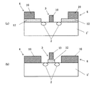
図1は、Zカット型の結晶基板1を用いた例であり、変調電極を構成する接地電極4に赤外透明導電膜12を用いた場合(図1(a)参照)と、変調電極を構成する信号電極3に赤外透明導電膜12を用いた場合(図1(b)参照)とを示している。
2はマッハツェンダー型導波路の分岐導波路であり、11はバッファ層、10は金属膜を各々示している。
Next, an example of a light control element having a novel structure using an infrared transparent conductive film will be described.
1 to 8 all show sectional views of an optical modulator having a light control element, particularly a Mach-Zehnder type waveguide.
FIG. 1 shows an example in which a Z-
図1の構成により、赤外透明導電膜12を用いる場合には、バッファ層11を省略することが可能であり、これにより光導波路に効率的に電界を印加できるため、低駆動電圧の光制御素子を実現することが可能となる。
With the configuration shown in FIG. 1, when the infrared transparent
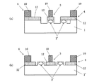
図2は、Xカット型の結晶基板1’を用いた例であり、変調電極を構成する接地電極4に赤外透明導電膜12を用いた場合(図2(a)参照)と、変調電極を構成する信号電極3に赤外透明導電膜12を用いた場合(図2(b)参照)とを示している。
図2の構成により、赤外透明導電膜12を用いる場合には、赤外透明導電膜を金属膜より光導波路2に近付けて配置することが可能となり、光導波路に効率的に電界が印加でき、低駆動電圧の光制御素子を実現することが可能となる。
FIG. 2 shows an example in which an
With the configuration shown in FIG. 2, when the infrared transparent
図3は、Zカット型の結晶基板1を用いた例であり、変調電極を構成する接地電極4を、赤外透明導電膜12と金属膜10との組合せで形成した場合(図3(a)参照)と、変調電極を構成する信号電極3を、赤外透明導電膜12と金属膜10との組合せで形成した場合(図3(b)参照)とを示している。
図3の場合においても、図1の構成と同様に、赤外透明導電膜12を用いる場合には、バッファ層11を省略することが可能であり、これにより光導波路に効率的に電界を印加できるため、低駆動電圧の光制御素子を実現することが可能となる。しかも、赤外透明導電膜に接して金属膜が配置されているため、接地電極(図3(a)の場合)又は信号電極(図3(b)の場合)の電気抵抗値を下げ、高周波領域におけるより高速な動作を可能とする光制御素子を提供することができる。
FIG. 3 shows an example in which the Z-
In the case of FIG. 3 as well, in the case of using the infrared transparent
図4は、Xカット型の結晶基板1’を用いた例であり、変調電極を構成する接地電極4を、赤外透明導電膜12と金属膜10との組合せで形成した場合(図4(a)参照)と、変調電極を構成する信号電極3を、赤外透明導電膜12と金属膜10との組合せで形成した場合(図4(b)参照)とを示している。
図4の場合においても、図2の構成と同様に、赤外透明導電膜を金属膜より光導波路2に近付けて配置することが可能となり、光導波路に効率的に電界が印加でき、低駆動電圧の光制御素子を実現することが可能となる。しかも、赤外透明導電膜に接して金属膜が配置されているため、接地電極(図4(a)の場合)又は信号電極(図4(b)の場合)の電気抵抗値を下げ、高周波領域におけるより高速な動作を可能とする光制御素子を提供することができる。
FIG. 4 shows an example in which an
In the case of FIG. 4 as well, as in the configuration of FIG. 2, the infrared transparent conductive film can be disposed closer to the
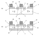
図5は、Xカット型の結晶基板1’を用いた例であり、変調電極を構成する接地電極4と信号電極3とを共に、赤外透明導電膜12と金属膜10との組合せで形成した場合を示している。
図5の場合には、赤外透明導電膜を金属膜より光導波路2に近付けて配置することが可能となり、光導波路に効率的に電界が印加でき、低駆動電圧の光制御素子を実現することが可能となる。特に、各電極の金属膜の間隔Wは、15μm以下、さらには10μm以下になるまで、金属膜間隔を狭めることが可能であり、従来の赤外透明導電膜を用いない場合(通常、金属膜間隔は20μm程度が限界である。)と比較し、間隔が約半分程度となり、より低駆動電圧で光制御素子を動作させることが可能となる。
なお、赤外透明導電膜に接して金属膜が配置されているため、各電極の電気抵抗値も下がることは、言うまでもない。
FIG. 5 shows an example using an
In the case of FIG. 5, the infrared transparent conductive film can be disposed closer to the
In addition, since the metal film is arrange | positioned in contact with an infrared transparent conductive film, it cannot be overemphasized that the electrical resistance value of each electrode also falls.
図6は、リッジ型光導波路2’を有する光制御素子の例を示す。
図6(a)は、Zカット型の結晶基板1を用いた例であり、変調電極を構成する接地電極4と信号電極3とを共に、赤外透明導電膜12と金属膜10との組合せで形成した場合を示している。図6(b)は、同様に、Xカット型の結晶基板1’を用いた例である。
FIG. 6 shows an example of a light control element having a ridge-type
FIG. 6A is an example using a Z-cut
リッジ型光導波路を用いた場合には、光の閉じ込めの大きな導波路を利用でき、従来と比較して導波路間隔の縮小が図れる効果とともに、赤外透明導電膜12が金属膜10よりも導波路2’に近接して配置できる相乗効果から、さらなる低駆動電圧型の光制御素子を提供することが可能となる。また、赤外透明導電膜であれば、光波の吸収なしにリッジ型光導波路2’の側面を含む領域において電極を形成することもできるため(不図示)、さらなる低駆動電圧化への効果がある。
なお、図6(a)における右側の接地電極4(赤外透明導電膜12)は、右側のリッジ型光導波路2’を形成する右側の溝を跨ぐように構成されているが、該溝に沿って赤外透明導電膜12を配置することも可能である。また、図6(b)における赤外透明導電膜12は、リッジ型光導波路2’の側面に接するように配置するすることも可能である。
When the ridge type optical waveguide is used, a waveguide with a large light confinement can be used, and the effect of reducing the waveguide interval compared to the conventional case, and the infrared transparent
The right ground electrode 4 (infrared transparent conductive film 12) in FIG. 6A is configured to straddle the right groove forming the right ridge-type
図7は、結晶基板の厚みが10μm以下の場合の例を示す。なお、光導波路にはリッジ型光導波路2’を用いた例を示している。
図7(a)は、Zカット型の結晶基板1を用いた例であり、基板1の上側に配置される変調電極は、赤外透明導電膜12と金属膜10との組合せで構成されている。また、図7(b)は、同様に、Xカット型の結晶基板1’を用いた例である。
FIG. 7 shows an example where the thickness of the crystal substrate is 10 μm or less. An example in which a ridge type
FIG. 7A shows an example in which a Z-
結晶基板の厚みが薄い場合には、赤外透明導電膜を使用することにより、基板の下側にも接地電極などの変調電極を形成することが可能である。図7(a)においては、Zカット型の結晶基板であるため、図面の縦方向の電界を生じるように、光導波路2’の下側に、接地電極となる裏面電極5を、赤外透明導電膜12で形成している。
図7(b)においては、Xカット型の結晶基板であるため、図面の横方向の電界を生じるように、光導波路2’の横方向側に、接地電極となる裏面電極5を、赤外透明導電膜12で形成している。
When the crystal substrate is thin, it is possible to form a modulation electrode such as a ground electrode on the lower side of the substrate by using an infrared transparent conductive film. In FIG. 7 (a), since it is a Z-cut type crystal substrate, a
In FIG. 7B, since it is an X-cut type crystal substrate, a
図7のような接地電極となる裏面電極5を用いる場合には、例えば、基板の上側の接地電極を不要にすることも可能であり、光制御素子をよりコンパクトなものに構成でき、基板の有効利用が可能になる。さらに、電極の配置が3次元となるため、光導波路に電界をより効率的に印加する電極の形状・配置が可能となり、光制御素子の作製再現性の向上を図ることも可能となる。
When the
図8は、分極反転を用いた例を示す。
図8はZカット型の結晶基板1を用いたものであり、基板1の上側に配置される変調電極は、赤外透明導電膜12と金属膜10との組合せで構成されている。結晶基板1の内部では、矢印A及びBで示したように、結晶内の自発分極の方向が境界線Cを境に、図面の左右で異なっている。
FIG. 8 shows an example using polarization reversal.
FIG. 8 uses a Z-cut
2がマッハツェンダー型光導波路などの分岐導波路である場合には、各分岐導波路2を含む結晶基板1内の自発分極の向きが、各分岐導波路毎に異なっているため、図8のように、2つの分岐導波路に共通の電極(信号電極3)で電界を印加すると、各分岐導波路に発生する電気光学効果は互いに逆向きとなる。これは、各分岐導波路に独立した電極を用意し、外部電気デバイスを用いて差動駆動を行うことと同じである。したがって、図8の構成により、容易に差動駆動が実現でき、より低駆動電圧での動作が可能な光制御素子を提供することが可能となる。
なお、図8(b)は、さらに、結晶基板の厚みが10μm以下の場合の例を示したものであり、上記効果に加え、図7の例と同様の効果も併せて有している。
When 2 is a branching waveguide such as a Mach-Zehnder type optical waveguide, the direction of spontaneous polarization in the
FIG. 8B shows an example in which the thickness of the crystal substrate is 10 μm or less, and has the same effect as the example of FIG. 7 in addition to the above effect.
(実施例1)
結晶性基板として、厚み500μmのXカット型LN基板を用い、Ti拡散法により光導波路を形成した。次に、該基板上にフォトリソグラフィー工程を経て、接地電極パターンが開口したフォトレジストマスクを形成し、DCマグネトロンスパッタ装置を用いて赤外透明導電膜を約1μm形成した後、有機溶剤中へ浸漬するリフトオフ法にてパターン形成を行なった。
赤外透明導電膜はDCパワー300W、酸素分圧1%の条件で行なった。
赤外透明膜を形成後、大気中にて180℃、1時間の熱処理を実施した。その後、レジストパターンをガイドとして電解メッキにより、高さ20μmのAu電極を信号電極として形成した。信号電極と接地電極の間隔は従来よりも5μm狭めたが、作製した光制御素子の挿入損失の増大は0.3dB以下であり、駆動電圧は従来のものと比較して20%低減した。
Example 1
An optical waveguide was formed by a Ti diffusion method using an X-cut LN substrate having a thickness of 500 μm as a crystalline substrate. Next, a photoresist mask having an opening in the ground electrode pattern is formed on the substrate through a photolithography process, and an infrared transparent conductive film is formed with a DC magnetron sputtering apparatus, and then immersed in an organic solvent. The pattern was formed by the lift-off method.
The infrared transparent conductive film was performed under the conditions of DC power of 300 W and oxygen partial pressure of 1%.
After forming the infrared transparent film, heat treatment was performed at 180 ° C. for 1 hour in the air. Thereafter, an Au electrode having a height of 20 μm was formed as a signal electrode by electrolytic plating using the resist pattern as a guide. Although the distance between the signal electrode and the ground electrode was narrowed by 5 μm compared to the conventional one, the increase in insertion loss of the manufactured light control element was 0.3 dB or less, and the drive voltage was reduced by 20% compared to the conventional one.
(実施例2)
結晶性基板として、厚み500μmのZカット型LN基板を用い、基板の一方の面に下部接地電極となる赤外透明導電膜を約1μm形成した。赤外透明導電膜の形成はDCパワー300W、酸素分圧1%のリアクティブスパッタ法で行ない、大気中にて180℃、1時間の熱処理を実施した。
次に、新たなZカットLN基板に、前記赤外透明導電膜付基板を、赤外透明導電膜を形成した面に接着剤塗布して互いを貼りあわせた。研磨用ジグに該基板を貼り付け固定後、前記赤外透明導電膜付基板の一方の面を、ラップ盤研磨機(キャリア:ガラス繊維入エポキシ樹脂 ラップ剤:GC#1200 20wt%aq)にて、速度35min−1、ラップ圧12.75〜9.81kPaの条件下において、基板の厚さがおよそ50μmとなるまで粗研磨する。この後、パット材質に不織布、加工液にはコロイダルシリカを用いたメカノケミカルポリッシング(CMP)により設定厚まで精密鏡面研磨を行った。基板の設定厚は4μmとした。
(Example 2)
A Z-cut LN substrate having a thickness of 500 μm was used as the crystalline substrate, and an infrared transparent conductive film serving as a lower ground electrode was formed on one surface of the substrate with a thickness of about 1 μm. The infrared transparent conductive film was formed by a reactive sputtering method with a DC power of 300 W and an oxygen partial pressure of 1%, and heat treatment was performed in the atmosphere at 180 ° C. for 1 hour.
Next, the substrate with infrared transparent conductive film was applied to a new Z-cut LN substrate with an adhesive applied to the surface on which the infrared transparent conductive film was formed, and then bonded together. After the substrate is pasted and fixed on a polishing jig, one surface of the substrate with the infrared transparent conductive film is fixed on a lapping machine polishing machine (carrier: epoxy resin containing glass fiber, lapping agent: GC # 1200 20 wt% aq). Then, rough polishing is performed until the thickness of the substrate becomes approximately 50 μm under conditions of a speed of 35 min −1 and a lap pressure of 12.75 to 9.81 kPa. Thereafter, precision mirror polishing was performed to a set thickness by mechanochemical polishing (CMP) using a nonwoven fabric as the pad material and colloidal silica as the processing liquid. The set thickness of the substrate was 4 μm.
該基板上にはマッハツェンダー型干渉系を有するリッジ型光導波路を形成した。形成にはフォトレジストをマスク材として使用したドライエッチング法を用いた。エッチング深さは2μmとした。該リッジ型導波路上には赤外透明導電膜を0.5μm形成しさらに、電界メッキ法により変調電極を形成した。 A ridge type optical waveguide having a Mach-Zehnder type interference system was formed on the substrate. For the formation, a dry etching method using a photoresist as a mask material was used. The etching depth was 2 μm. An infrared transparent conductive film of 0.5 μm was formed on the ridge-type waveguide, and a modulation electrode was formed by electroplating.
(比較例1)
前記下部接地電極として形成した赤外透明導電膜の代わりに、SiO2バッファ層0.5μmとAu電極1μmを形成、また、前記リッジ型導波路上に形成した赤外透明導電膜の代わりにSiO2バッファ層0.5μmを形成する以外は、実施例2と同様にして光制御素子を作成した。
(Comparative Example 1)
Instead of the infrared transparent conductive film formed as the lower ground electrode, an SiO 2 buffer layer of 0.5 μm and an Au electrode of 1 μm are formed, and instead of the infrared transparent conductive film formed on the ridge-type waveguide, SiO 2 A light control element was produced in the same manner as in Example 2 except that 0.5 buffer layer was formed.
実施例2及び比較例1における光制御素子の駆動電圧の比較を行なったところ、比較例1ではVπL=6.1Vcmであるのに対し、実施例2ではVπL=3.7Vcmと大幅な低駆動電圧化が図られた。 When the drive voltage of the light control element in Example 2 and Comparative Example 1 was compared, VπL = 6.1 Vcm in Comparative Example 1, whereas VπL = 3.7 Vcm in Example 2 was significantly low. Voltageization was achieved.
本発明に係る光制御素子によれば、InとTiの複合酸化物膜からなる赤外透明導電膜を用いることで、光波の挿入損失の増大を招くことなしに、駆動電圧の大幅な低減が図れ、新たな光制御素子構造を提案することが可能となる。さらに、本発明により、情報網の整備に伴い増大している光制御素子の消費電力を、大幅に低減することが可能となる。 According to the light control element of the present invention, the use of the infrared transparent conductive film made of a composite oxide film of In and Ti can significantly reduce the drive voltage without increasing the insertion loss of light waves. This makes it possible to propose a new light control element structure. Furthermore, according to the present invention, it is possible to significantly reduce the power consumption of the light control element, which has been increasing with the improvement of the information network.
1 Zカット型結晶基板
1’ Xカット型結晶基板
2 光導波路
2’ リッジ型光導波路
3 信号電極
4 接地電極
5 裏面電極
10 金属膜
11 バッファ層
12 赤外透明導電膜
DESCRIPTION OF SYMBOLS 1 Z cut type crystal substrate 1 'X cut
Claims (11)
該変調電極を構成する信号電極と接地電極のうち、少なくとも一方にはTiとInの複合酸化物からなる赤外透明導電膜が用いられることを特徴とする光制御素子。 In a light control element having a crystal substrate having an electro-optic effect, an optical waveguide formed on the substrate, and a modulation electrode for modulating light passing through the optical waveguide,
An optical control element, wherein an infrared transparent conductive film made of a composite oxide of Ti and In is used for at least one of a signal electrode and a ground electrode constituting the modulation electrode.
11. The light control element according to claim 1, wherein the light control element is used in a region having a wavelength longer than an optical communication wavelength band.
Priority Applications (1)
| Application Number | Priority Date | Filing Date | Title |
|---|---|---|---|
| JP2006100527A JP2007272122A (en) | 2006-03-31 | 2006-03-31 | Optical control element |
Applications Claiming Priority (1)
| Application Number | Priority Date | Filing Date | Title |
|---|---|---|---|
| JP2006100527A JP2007272122A (en) | 2006-03-31 | 2006-03-31 | Optical control element |
Publications (1)
| Publication Number | Publication Date |
|---|---|
| JP2007272122A true JP2007272122A (en) | 2007-10-18 |
Family
ID=38674943
Family Applications (1)
| Application Number | Title | Priority Date | Filing Date |
|---|---|---|---|
| JP2006100527A Pending JP2007272122A (en) | 2006-03-31 | 2006-03-31 | Optical control element |
Country Status (1)
| Country | Link |
|---|---|
| JP (1) | JP2007272122A (en) |
Cited By (6)
| Publication number | Priority date | Publication date | Assignee | Title |
|---|---|---|---|---|
| JP2017161595A (en) * | 2016-03-07 | 2017-09-14 | 住友大阪セメント株式会社 | Waveguide type light-emitting element |
| CN108693664A (en) * | 2017-03-31 | 2018-10-23 | 住友大阪水泥股份有限公司 | Optical modulator |
| CN111936917A (en) * | 2018-03-29 | 2020-11-13 | 住友大阪水泥股份有限公司 | Optical element |
| WO2023053332A1 (en) * | 2021-09-30 | 2023-04-06 | 住友大阪セメント株式会社 | Optical waveguide element, and optical transmission apparatus and optical modulation device using same |
| WO2023188194A1 (en) * | 2022-03-30 | 2023-10-05 | 住友大阪セメント株式会社 | Optical waveguide element, and optical modulation device and optical transmission apparatus using same |
| WO2024069952A1 (en) * | 2022-09-30 | 2024-04-04 | 住友大阪セメント株式会社 | Optical waveguide element, optical modulation device using same, and optical transmission device |
Citations (5)
| Publication number | Priority date | Publication date | Assignee | Title |
|---|---|---|---|---|
| JPH05142504A (en) * | 1991-11-19 | 1993-06-11 | Fujitsu Ltd | Optical transmitter |
| JPH1039266A (en) * | 1995-11-28 | 1998-02-13 | Nippon Telegr & Teleph Corp <Ntt> | Optical control device |
| JP2003215519A (en) * | 2001-11-16 | 2003-07-30 | Ngk Insulators Ltd | Optical waveguide device, and traveling wave form optical modulator |
| JP2004341147A (en) * | 2003-05-15 | 2004-12-02 | Ngk Insulators Ltd | Optical waveguide device and traveling waveform optical modulator |
| WO2006004139A1 (en) * | 2004-06-30 | 2006-01-12 | Sumitomo Metal Mining Co., Ltd. | Waveguide type light control element and manufacturing method thereof |
-
2006
- 2006-03-31 JP JP2006100527A patent/JP2007272122A/en active Pending
Patent Citations (5)
| Publication number | Priority date | Publication date | Assignee | Title |
|---|---|---|---|---|
| JPH05142504A (en) * | 1991-11-19 | 1993-06-11 | Fujitsu Ltd | Optical transmitter |
| JPH1039266A (en) * | 1995-11-28 | 1998-02-13 | Nippon Telegr & Teleph Corp <Ntt> | Optical control device |
| JP2003215519A (en) * | 2001-11-16 | 2003-07-30 | Ngk Insulators Ltd | Optical waveguide device, and traveling wave form optical modulator |
| JP2004341147A (en) * | 2003-05-15 | 2004-12-02 | Ngk Insulators Ltd | Optical waveguide device and traveling waveform optical modulator |
| WO2006004139A1 (en) * | 2004-06-30 | 2006-01-12 | Sumitomo Metal Mining Co., Ltd. | Waveguide type light control element and manufacturing method thereof |
Cited By (8)
| Publication number | Priority date | Publication date | Assignee | Title |
|---|---|---|---|---|
| JP2017161595A (en) * | 2016-03-07 | 2017-09-14 | 住友大阪セメント株式会社 | Waveguide type light-emitting element |
| CN108693664A (en) * | 2017-03-31 | 2018-10-23 | 住友大阪水泥股份有限公司 | Optical modulator |
| JP2018173450A (en) * | 2017-03-31 | 2018-11-08 | 住友大阪セメント株式会社 | Waveguide type optical element |
| US10228605B2 (en) | 2017-03-31 | 2019-03-12 | Sumitomo Osaka Cement Co., Ltd. | Waveguide optical element |
| CN111936917A (en) * | 2018-03-29 | 2020-11-13 | 住友大阪水泥股份有限公司 | Optical element |
| WO2023053332A1 (en) * | 2021-09-30 | 2023-04-06 | 住友大阪セメント株式会社 | Optical waveguide element, and optical transmission apparatus and optical modulation device using same |
| WO2023188194A1 (en) * | 2022-03-30 | 2023-10-05 | 住友大阪セメント株式会社 | Optical waveguide element, and optical modulation device and optical transmission apparatus using same |
| WO2024069952A1 (en) * | 2022-09-30 | 2024-04-04 | 住友大阪セメント株式会社 | Optical waveguide element, optical modulation device using same, and optical transmission device |
Similar Documents
| Publication | Publication Date | Title |
|---|---|---|
| JP4589354B2 (en) | Light modulation element | |
| JP4445977B2 (en) | Light control element | |
| JP5298849B2 (en) | Light control element | |
| US6721085B2 (en) | Optical modulator and design method therefor | |
| US8600197B2 (en) | Optical control device | |
| JP2008089936A (en) | Optical control element | |
| JP4745432B2 (en) | Optical waveguide device | |
| JP2007272122A (en) | Optical control element | |
| JPWO2005019913A1 (en) | Optical waveguide device and traveling wave optical modulator | |
| JP2014006348A (en) | Optical modulator | |
| JPH09211402A (en) | Broad-band light modulator | |
| CN213581652U (en) | Optical waveguide element, optical modulator, optical modulation module, and optical transmission device | |
| US20110013863A1 (en) | Optical waveguide element module | |
| JPH05196972A (en) | Waveguide type optical directional coupler | |
| US6768570B2 (en) | Optical modulator | |
| US7218819B2 (en) | Electrode systems for optical modulation and optical modulators | |
| JP2010085789A (en) | Optical waveguide element | |
| US7409114B2 (en) | Optical modulator | |
| JP2001174766A (en) | Waveguide type optical modulator | |
| JP2001004967A (en) | Optical waveguide element | |
| JP2800339B2 (en) | Method of manufacturing optical modulator | |
| JPH06222403A (en) | Directional coupling type optical waveguide | |
| JP3019278B2 (en) | Waveguide type optical device | |
| JP2809112B2 (en) | Light control device and manufacturing method thereof | |
| JP2006276519A (en) | Waveguide type optical device |
Legal Events
| Date | Code | Title | Description |
|---|---|---|---|
| A621 | Written request for application examination |
Free format text: JAPANESE INTERMEDIATE CODE: A621 Effective date: 20080729 |
|
| A131 | Notification of reasons for refusal |
Free format text: JAPANESE INTERMEDIATE CODE: A131 Effective date: 20100817 |
|
| A521 | Request for written amendment filed |
Free format text: JAPANESE INTERMEDIATE CODE: A523 Effective date: 20101018 |
|
| A02 | Decision of refusal |
Free format text: JAPANESE INTERMEDIATE CODE: A02 Effective date: 20101109 |