JP2007258671A - Drive circuit of light-emitting diode - Google Patents
Drive circuit of light-emitting diode Download PDFInfo
- Publication number
- JP2007258671A JP2007258671A JP2006305705A JP2006305705A JP2007258671A JP 2007258671 A JP2007258671 A JP 2007258671A JP 2006305705 A JP2006305705 A JP 2006305705A JP 2006305705 A JP2006305705 A JP 2006305705A JP 2007258671 A JP2007258671 A JP 2007258671A
- Authority
- JP
- Japan
- Prior art keywords
- module
- voltage
- signal
- driving
- light emitting
- Prior art date
- Legal status (The legal status is an assumption and is not a legal conclusion. Google has not performed a legal analysis and makes no representation as to the accuracy of the status listed.)
- Pending
Links
Images


Classifications
-
- G—PHYSICS
- G09—EDUCATION; CRYPTOGRAPHY; DISPLAY; ADVERTISING; SEALS
- G09G—ARRANGEMENTS OR CIRCUITS FOR CONTROL OF INDICATING DEVICES USING STATIC MEANS TO PRESENT VARIABLE INFORMATION
- G09G3/00—Control arrangements or circuits, of interest only in connection with visual indicators other than cathode-ray tubes
- G09G3/20—Control arrangements or circuits, of interest only in connection with visual indicators other than cathode-ray tubes for presentation of an assembly of a number of characters, e.g. a page, by composing the assembly by combination of individual elements arranged in a matrix no fixed position being assigned to or needed to be assigned to the individual characters or partial characters
- G09G3/34—Control arrangements or circuits, of interest only in connection with visual indicators other than cathode-ray tubes for presentation of an assembly of a number of characters, e.g. a page, by composing the assembly by combination of individual elements arranged in a matrix no fixed position being assigned to or needed to be assigned to the individual characters or partial characters by control of light from an independent source
- G09G3/3406—Control of illumination source
-
- H—ELECTRICITY
- H05—ELECTRIC TECHNIQUES NOT OTHERWISE PROVIDED FOR
- H05B—ELECTRIC HEATING; ELECTRIC LIGHT SOURCES NOT OTHERWISE PROVIDED FOR; CIRCUIT ARRANGEMENTS FOR ELECTRIC LIGHT SOURCES, IN GENERAL
- H05B45/00—Circuit arrangements for operating light-emitting diodes [LED]
- H05B45/10—Controlling the intensity of the light
-
- H—ELECTRICITY
- H05—ELECTRIC TECHNIQUES NOT OTHERWISE PROVIDED FOR
- H05B—ELECTRIC HEATING; ELECTRIC LIGHT SOURCES NOT OTHERWISE PROVIDED FOR; CIRCUIT ARRANGEMENTS FOR ELECTRIC LIGHT SOURCES, IN GENERAL
- H05B45/00—Circuit arrangements for operating light-emitting diodes [LED]
- H05B45/30—Driver circuits
- H05B45/37—Converter circuits
- H05B45/3725—Switched mode power supply [SMPS]
- H05B45/38—Switched mode power supply [SMPS] using boost topology
-
- H—ELECTRICITY
- H05—ELECTRIC TECHNIQUES NOT OTHERWISE PROVIDED FOR
- H05B—ELECTRIC HEATING; ELECTRIC LIGHT SOURCES NOT OTHERWISE PROVIDED FOR; CIRCUIT ARRANGEMENTS FOR ELECTRIC LIGHT SOURCES, IN GENERAL
- H05B45/00—Circuit arrangements for operating light-emitting diodes [LED]
- H05B45/30—Driver circuits
- H05B45/37—Converter circuits
- H05B45/3725—Switched mode power supply [SMPS]
- H05B45/382—Switched mode power supply [SMPS] with galvanic isolation between input and output
-
- H—ELECTRICITY
- H05—ELECTRIC TECHNIQUES NOT OTHERWISE PROVIDED FOR
- H05B—ELECTRIC HEATING; ELECTRIC LIGHT SOURCES NOT OTHERWISE PROVIDED FOR; CIRCUIT ARRANGEMENTS FOR ELECTRIC LIGHT SOURCES, IN GENERAL
- H05B45/00—Circuit arrangements for operating light-emitting diodes [LED]
- H05B45/30—Driver circuits
- H05B45/37—Converter circuits
- H05B45/3725—Switched mode power supply [SMPS]
- H05B45/385—Switched mode power supply [SMPS] using flyback topology
-
- H—ELECTRICITY
- H05—ELECTRIC TECHNIQUES NOT OTHERWISE PROVIDED FOR
- H05B—ELECTRIC HEATING; ELECTRIC LIGHT SOURCES NOT OTHERWISE PROVIDED FOR; CIRCUIT ARRANGEMENTS FOR ELECTRIC LIGHT SOURCES, IN GENERAL
- H05B45/00—Circuit arrangements for operating light-emitting diodes [LED]
- H05B45/50—Circuit arrangements for operating light-emitting diodes [LED] responsive to malfunctions or undesirable behaviour of LEDs; responsive to LED life; Protective circuits
-
- G—PHYSICS
- G09—EDUCATION; CRYPTOGRAPHY; DISPLAY; ADVERTISING; SEALS
- G09G—ARRANGEMENTS OR CIRCUITS FOR CONTROL OF INDICATING DEVICES USING STATIC MEANS TO PRESENT VARIABLE INFORMATION
- G09G2320/00—Control of display operating conditions
- G09G2320/06—Adjustment of display parameters
- G09G2320/0626—Adjustment of display parameters for control of overall brightness
- G09G2320/064—Adjustment of display parameters for control of overall brightness by time modulation of the brightness of the illumination source
-
- G—PHYSICS
- G09—EDUCATION; CRYPTOGRAPHY; DISPLAY; ADVERTISING; SEALS
- G09G—ARRANGEMENTS OR CIRCUITS FOR CONTROL OF INDICATING DEVICES USING STATIC MEANS TO PRESENT VARIABLE INFORMATION
- G09G2330/00—Aspects of power supply; Aspects of display protection and defect management
- G09G2330/04—Display protection
-
- Y—GENERAL TAGGING OF NEW TECHNOLOGICAL DEVELOPMENTS; GENERAL TAGGING OF CROSS-SECTIONAL TECHNOLOGIES SPANNING OVER SEVERAL SECTIONS OF THE IPC; TECHNICAL SUBJECTS COVERED BY FORMER USPC CROSS-REFERENCE ART COLLECTIONS [XRACs] AND DIGESTS
- Y02—TECHNOLOGIES OR APPLICATIONS FOR MITIGATION OR ADAPTATION AGAINST CLIMATE CHANGE
- Y02B—CLIMATE CHANGE MITIGATION TECHNOLOGIES RELATED TO BUILDINGS, e.g. HOUSING, HOUSE APPLIANCES OR RELATED END-USER APPLICATIONS
- Y02B20/00—Energy efficient lighting technologies, e.g. halogen lamps or gas discharge lamps
- Y02B20/30—Semiconductor lamps, e.g. solid state lamps [SSL] light emitting diodes [LED] or organic LED [OLED]
Abstract
Description
本発明は複数の発光ダイオード(LED)のための駆動技術に関するものである。特に、本発明は、バックライトモジュールに用いられるLEDのための駆動技術に関するものである。 The present invention relates to a driving technique for a plurality of light emitting diodes (LEDs). In particular, the present invention relates to a driving technique for an LED used in a backlight module.
従来のバックライトモジュールにおいて、冷陰極管が光源として一般に用いられている。しかし近年では、光電素子技術の発展にともない、発光ダイオードが小さなサイズ、低動作電圧、長寿命、彩度等、多くの利点を持っている。したがって、バックライトモジュールの光源としてLEDを用いることは、新しい選択肢の一つとなってきた。 In a conventional backlight module, a cold cathode tube is generally used as a light source. However, in recent years, with the development of photoelectric device technology, light emitting diodes have many advantages such as small size, low operating voltage, long life, and saturation. Therefore, using LEDs as the light source of the backlight module has become one of the new options.
製造過程の要因によって、同一基盤上のLEDでさえ異なる電気的特性を有し、並列接続されたLEDの輝度は実際に適用されたときに全く異なる。製造過程の歩留まりを良くし製造コストを削減するために、現在のLEDバックライトモジュールに用いられるLEDは主に直列接続LEDを光源として用いるので、それぞれのLEDを通る電流は等しく、輝度は実質的に等しい。 Due to manufacturing process factors, even LEDs on the same substrate have different electrical characteristics, and the brightness of LEDs connected in parallel is quite different when actually applied. In order to improve the yield of the manufacturing process and reduce the manufacturing cost, the LEDs used in the current LED backlight module mainly use series-connected LEDs as light sources, so that the currents through the respective LEDs are equal and the luminance is substantially be equivalent to.
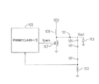
図1は、従来のLEDバックライトモジュールの回路図である。図1において、従来のLEDバックライトモジュールでは、複数の直列接続されたLED101が光源として用いられ、抵抗103を介して接地されている。
FIG. 1 is a circuit diagram of a conventional LED backlight module. In FIG. 1, in a conventional LED backlight module, a plurality of
図1において、時間の経過によるLED101の輝度の変化を減らすために、パルス幅変調(PWM)コントローラ105がバックライトモジュールに配置され、LED101の輝度を制御するようにPWM信号Vpwmを発生する。従来のバックライトモジュールにおいて、PWMコントローラ105はPWM信号VpwmをNMOSトランジスタ107のゲートに送る。NMOSトランジスタ107のドレイン端は、インダクタ109を介して電源VDDに接続され、ショトキ・ダイオード111を介して直列に接続されたLED101及びコンデンサ113に接続される。また、NMOSトランジスタ107のソース及びコンデンサ113の他端は接地される。
In FIG. 1, a pulse width modulation (PWM)
さらに、LED101の電流を検出するために、PWMコントローラ105はまた、LED101と抵抗103との結節点に接続される。このように、LED101の輝度を変調するために、検出された結果に応じてPWMコントローラ105はPWM信号Vpwmのデューティ・サイクルを決定する。
Further, in order to detect the current of the
図1に示されたブースト回路は、各LED101を駆動するために、電源VDDより高い出力DC電圧Voutを発生する。しかし、フラットパネルディスプレイの寸法が大きくなるにつれて、バックライトモジュールの寸法もまた大きくされる必要があり、より多くのLED101が必要とされ、求められる駆動電圧もまた高くなってきた。図1におけるブースト回路によって提供されるブーストの拡大比(Vout/VDD)は、そのような高駆動電圧を十分には提供しない。したがって、ブースト要素としてインダクタ109を用いる設計は電源VDDの値に確実に制限され、連続して直列接続されたLED101を加えるための必要条件はより柔軟には満足されることができない。
The boost circuit shown in FIG. 1 generates an output DC voltage Vout higher than the power supply VDD in order to drive each
さらに、直列接続されたLED101の数を増加することによって電圧保護に対しての要件を有するために、その駆動電圧もまた増加する。ある電圧値以下に駆動電圧を固定するために、現在のLEDバックライトモジュールはショトキ・ダイオードを用いるだけである。しかしながら、駆動電圧がより高いときより高い降伏電圧を有するショトキ・ダイオードが必要となる。このように、要素のコストが増えるだけでなく出力電圧が超えた時に電圧保護以上にはならずに高電圧が連続的に出力されるので、その結果他の要素が損傷してしまう。
Furthermore, in order to have a requirement for voltage protection by increasing the number of
したがって本発明は、複数の直列接続されたLEDを駆動することができ、多くの異なる寸法のディスプレイパネルにおいて用いられ得るLED駆動回路を提供する。 Thus, the present invention provides an LED drive circuit that can drive a plurality of series connected LEDs and can be used in many different sized display panels.
本発明によって提供されるLEDの駆動回路は、変圧器、駆動モジュール及び保護モジュールを備えている。変圧器は一次コイル及び二次コイルを備えている。本発明において、一次コイルの第一端は電源に接続され、二次コイルの第一端はLEDに接続され、二次コイルの第二端は接地される。さらに、変圧器の一次コイルの第二端は駆動モジュールに接続され、駆動モジュールは電力を変圧器に送るかどうかをPWM信号及びエラー信号に応じて決定する。保護モジュールは二次コイルに接続される。変圧器によってLEDに出力された駆動電圧が第一プリセット電圧より低い、あるいは第二プリセット電圧より大きいとき、電力の出力を停止するように、保護モジュールはエラー信号を駆動モジュールに発生する。 The LED driving circuit provided by the present invention includes a transformer, a driving module, and a protection module. The transformer includes a primary coil and a secondary coil. In the present invention, the first end of the primary coil is connected to the power source, the first end of the secondary coil is connected to the LED, and the second end of the secondary coil is grounded. Further, the second end of the primary coil of the transformer is connected to the drive module, and the drive module determines whether to send power to the transformer according to the PWM signal and the error signal. The protection module is connected to the secondary coil. When the drive voltage output to the LED by the transformer is lower than the first preset voltage or greater than the second preset voltage, the protection module generates an error signal to the drive module to stop the output of power.
本発明の一実施例において、上述した保護モジュールは、第一コンパレータ、第一タイマー及び初期タイマーを備えている。第一コンパレータは駆動電圧が第一プリセット電圧より低いかどうかを決定し、第一比較結果を出力するのに用いられる。第一タイマーは、第一比較結果を受け取り、第一プリセットタイムの間に駆動電圧が第一プリセット電圧よりも低い時に、第一タイミング信号を発生するのに用いられる。本発明において、第一タイマーは、駆動回路が起動されるまでのある時間帯に、使用不可能の状態にある。さらに、その時間帯に駆動回路が起動されるとき、第一タイマーを使用可能にするために、初期タイマーは初期タイミング信号を発生するのに用いられる。第一タイマーによって出力された第一タイミング値はラッチに送られ、それからラッチを介してインバータに送られた後に駆動モジュールへ出力される。 In one embodiment of the present invention, the above-described protection module includes a first comparator, a first timer, and an initial timer. The first comparator determines whether the driving voltage is lower than the first preset voltage and is used to output a first comparison result. The first timer receives the first comparison result and is used to generate a first timing signal when the driving voltage is lower than the first preset voltage during the first preset time. In the present invention, the first timer is in an unusable state during a certain time period until the drive circuit is activated. In addition, when the drive circuit is activated during that time period, the initial timer is used to generate an initial timing signal to enable the first timer. The first timing value output by the first timer is sent to the latch, and then sent to the inverter via the latch before being output to the drive module.
また、保護モジュールは、第二コンパレータ及び第二タイマーをさらに備えている。第二コンパレータは駆動電圧が第二プリセット電圧より高いかどうかを決定し、第二比較結果を出力するのに用いられる。第二タイマーは第二比較結果を受け取り、第二プリセットタイムの間に駆動電圧が第二プリセット電圧よりも大きい時、第二タイミング信号を発生するのに用いられる。第二タイミング信号はORゲートに送られる。ORゲートは第二タイミング信号を受け取るだけでなく、第一タイミング信号をも受け取る。さらに、ORゲートの出力はラッチへ送られる。 The protection module further includes a second comparator and a second timer. The second comparator determines whether the drive voltage is higher than the second preset voltage and is used to output a second comparison result. The second timer receives the second comparison result and is used to generate a second timing signal when the driving voltage is greater than the second preset voltage during the second preset time. The second timing signal is sent to the OR gate. The OR gate not only receives the second timing signal but also receives the first timing signal. In addition, the output of the OR gate is sent to a latch.
他の実施例では、上述の第二コンパレータは駆動電圧を第二プリセット電圧と比較し、ここでは、第二コンパレータは高いヒステリシスを有する。駆動電圧が、一つ以上のヒステリシス電圧だけ第二プリセット電圧よりも大きいときに、第二コンパレータはORゲートに高いレベルの出力を発生する。このORゲートは上述したラッチの出力を受け取り、このORゲートの出力は上述のインバータに送られる。 In another embodiment, the second comparator described above compares the drive voltage with a second preset voltage, where the second comparator has a high hysteresis. When the drive voltage is greater than the second preset voltage by one or more hysteresis voltages, the second comparator generates a high level output at the OR gate. The OR gate receives the output of the latch described above, and the output of the OR gate is sent to the inverter described above.
本発明によって提供されるバックライトモジュールは光源モジュールを備えている。さらに、本発明のバックライトモジュールは、上述の駆動回路によって光を発するために駆動される。 The backlight module provided by the present invention includes a light source module. Furthermore, the backlight module of the present invention is driven to emit light by the drive circuit described above.
本発明によって提供されるLED駆動回路は、本発明の駆動回路が高すぎるあるいは低すぎる駆動電圧を出力することを妨ぐことのできる、好適な保護モジュールを有する。 The LED drive circuit provided by the present invention has a suitable protection module that can prevent the drive circuit of the present invention from outputting a drive voltage that is too high or too low.
本発明はまた、光源を駆動するために電源を駆動電圧に変換する変圧器を用いるので、本発明は駆動電圧の値を直列接続されたLEDの数によって制限されることなく調節することができ得る。したがって、本発明は応用においてより自由度が高い。 The present invention also uses a transformer that converts a power source to a driving voltage to drive the light source, so that the present invention can adjust the value of the driving voltage without being limited by the number of LEDs connected in series. obtain. Therefore, the present invention is more flexible in application.
本発明の、前述のあるいは他の目的、特徴及び利点を達成するために、好適な実施例は図を参照して以下に詳細に説明される。 In order to achieve the foregoing and other objects, features and advantages of the present invention, preferred embodiments will be described in detail below with reference to the drawings.
前述の一般的な記載及び続く詳細にわたる説明の両者は典型的なものであり、請求されている本発明のさらなる説明を提供することが意図されている。 Both the foregoing general description and the following detailed description are exemplary and are intended to provide further explanation of the claimed invention.
本発明の好適な実施例は、本発明の種々の好ましい実施例を示す添付の図の引用例とともに、以下に詳細に説明される。本発明はまた、多くの異なる方法によって達成され得、ここに示された実施例には限定されない。ここに実施例を提供することの目的は、当業者が本発明の目的を十分に把握できるようにすることである。以下において、同様な符号は、同様な要素を表す。 Preferred embodiments of the present invention are described in detail below, along with citations in the accompanying drawings showing various preferred embodiments of the present invention. The present invention can also be achieved in many different ways and is not limited to the examples shown here. The purpose of providing examples herein is to enable those skilled in the art to fully understand the purpose of the present invention. In the following, like symbols represent like elements.
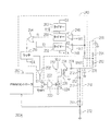
図2Aは、本発明第一の実施例によるバックライトモジュールの回路図である。図2Aを参照すると、本発明によって提供されるバックライトモジュール200Aは、光源モジュール210と駆動モジュール220、変圧器230及び保護モジュール240によって構成される駆動回路とを備えている。本発明の実施例では、光源モジュール210は複数の直列接続されたLED212によって形成されることができる。変圧器230は、より多くの直列にあるLEDを駆動するより高いDC駆動電圧を提供するために、駆動電源を増幅することが可能であるブースターにより実現される。
FIG. 2A is a circuit diagram of the backlight module according to the first embodiment of the present invention. Referring to FIG. 2A, the backlight module 200 </ b> A provided by the present invention includes a light source module 210, a
特に、各LED212のカソード端は、次のLED212のアノード端に接続され、最後のLED212は、抵抗272を介してグラウンドに接続される。当業者が理解すべきことは、バックライトモジュール200AにおけるLED212は、白色光LED、赤色光LED、青色光LED、緑色光LEDを含んでいる、ということである。
In particular, the cathode end of each
図2Aを参照すると、変圧器230は一次コイル232及び二次コイル234を、1/nの比で有する。本実施例において、一次コイル232の第一端は電源VDDに接続され、第二端は駆動モジュール220に接続される。さらに、二次コイル234の第一端はダイオード274を介して光源モジュール210に接続され、例えば、第一LED212のアノード端に接続され、二次コイル234の第二端は接地している。好適な状況において、ダイオード274はショトキ・ダイオードによって達成され得る。
Referring to FIG. 2A, the transformer 230 has a
二次コイル234の第一端はまた、光源モジュール210に加えて保護モジュール240に接続され、コンデンサ276を介してグラウンドへ接続される。保護モジュール240の出力は駆動モジュール220へ送られ、保護モジュール240の出力に応じて電源VDDの電力の変圧器230への出力を停止するかどうかを駆動モジュール220は決定する。
The first end of the
駆動モジュール220はANDゲート222及びNMOSトランジスタ224を含んでもよい。ANDゲート222はPWM信号Vpwm及び保護モジュール240の出力を受け取る。さらに、ANDゲートの出力はNMOSトランジスタ224のゲート端へ接続され、NMOSトランジスタ224のドレインは一次コイル232の第二端に接続され、そのソースは接地されている。本発明の実施例において、ANDゲートはまた起動制御信号EA(エラーリセット信号、とも呼ばれる)を受け取り得る。起動制御信号EAはまた第一タイマー252、第二タイマー260、及びラッチ256へ同時に出力される。起動される前あるいはリスタートされる時に、EA=0という信号がバックライトモジュール200Aに出力され、NMOSトランジスタ224、第一タイマー252、第二タイマー260及びラッチ256がリセットされる。バックライトモジュール200Aが起動されたあるいはリスタートされた後には、EA=1となり、NMOSトランジスタ224、第一タイマー252、第二タイマー260、及びラッチ256を起動する。
The
本実施例において、PWM信号VpwmはPWMコントローラ280によって発生され得る。さらに、PWMコントローラ280は、光源モジュール210と抵抗272との結節点の電圧を検出する、つまり、光源モジュール210を流れる電流を検出する。したがって、光源モジュール210が安定した輝度を有するように、PWMコントローラ280は、光源モジュール210の検出信号に応じてPWM信号Vpwmのデューティ・サイクルを制御することができる。もちろん、PWMコントローラ280は、光源モジュール210の電圧の検出信号(例えば、電圧検出モジュール290に接続された)に応じて、PWM信号Vpwmを発生することもできる。
In this embodiment, the PWM signal Vpwm can be generated by the
電圧検出モジュール290は、抵抗292及び294を直列で有し、そこでは、抵抗292の第一端がダイオード274のカソード端に接続され、二次コイル234の第一端に、ダイオード274を介して接続される。さらに、抵抗292の第二端は、コンパレータ246の反転入力とコンパレータ248の非反転入力とに接続される。駆動モジュール220、保護モジュール240、PWMコントローラ280及び電圧検出モジュール290は集積回路チップにおいて統合され得る。これとは別に、バックライトモジュールの設計者が抵抗292及び294の比を、様々なバックライトモジュールに適合するようにより自由に割り当てることができるように、電圧検出モジュール290は集積回路チップから独立させることもできる。
The
さらに、コンパレータ246の非反転入力は、プリセット電圧Vr1を受け取り、コンパレータ248の反転入力はプリセット入力Vr2を受け取る。それによって、コンパレータ246は駆動電圧VOUTをプリセット電圧Vr1と比較し、比較結果R1をタイマー250に発生する。同様に、コンパレータ248は駆動電圧VOUTをプリセット電圧Vr2と比較し、比較結果R2をタイマー252に発生する。本実施例において、コンパレータ246及び248はそれぞれ駆動電圧VOUTが低くあるいは高くなり過ぎたか、そしてプリセット電圧Vr1がプリセット電圧Vr2よりも低いかどうかを検出するために用いられる。
Further, the non-inverting input of the
次に、バックライトモジュール200Aの動作プロセスが以下に説明される。
Next, the operation process of the
バックライトモジュール200Aがまさに起動された時、エラーリセット信号EAは高いレベル状態(すなわち、EA=1)にある。本発明のバックライトモジュール200Aがまさに起動された時に、低すぎる駆動電圧VOUTによってエラーと見なされるといった状況を避けるために、タイマー260が保護モジュール240に配置される。バックライトモジュール200Aがただ起動された時、タイマー260はT0=0といった低いレベルの信号を出力する。ここで、タイマー250は、使用不可能な状態になるように、T0=0といった低いレベルの信号を受け取り、この時点で、T1=0となる。
When the
さらに、タイマー252は、EA=1を受け取ることによって起動される。この時、駆動電圧VOUTがプリセット電圧Vr2よりも低く、コンパレータ248はR2=0を出力するので、タイマー252はT2=0を出力する。したがって、ORゲート254は、T1=0とT2=0を受け取った後に、低レベル信号を出力する。EA=1を受け取り起動された後には、ラッチ256は、ORゲート254の低レベル信号を受け取って低レベル信号を出力し、それからインバータ258はE1=1といった高レベル信号を出力する。このように、バックライトモジュール200Aがまさに起動されたときには、EA=1及びE1=1となる。NMOSトランジスタ224のオン−オフ切り換えを制御するために、ANDゲート222はPWMコントローラ280に応じてPWM信号Vpwmを発生し、光源モジュール210を駆動するために、変圧器230は電源VDDを駆動電圧VOUTに変換することができる。
In addition,
タイマー260が第一プリセットタイムを計測した後に、EAがまだ“1”といった高レベル信号のまま残っているならば、タイマー260はT0=1といった高レベル信号を出力する。このように、タイマー250はT0=1といった信号を受け取り、動作を始める。タイマー260の好ましい第一プリセットタイムは、バックライトモジュール200Aを駆動するのに必要な時間に等しいか、より長いことである。第一プリセットタイムの後、光源モジュール210は正常に動作を始める。したがって、タイマー250が動作し始める時、電圧検出モジュール290は、プリセット電圧Vr1よりも大きく、プリセット電圧Vr2よりも低い検出信号を出力する。このように、通常動作状態に入った後には、コンパレータ246及び248の出力信号R1及びR2は、ともに低レベル信号なので、タイマー250及び252の出力信号T1及びT2もまた低レベル信号である。したがって、通常起動においては、信号E1を低論理水準“0”のままにするために、ラッチ256は低レベル信号を出力し続ける。
After the
しかしながら、起動の失敗あるいは他のエラーによって駆動電圧VOUTが低すぎるとき、例えば、ユーザーが不注意に変圧器230の二次コイル234の末端を触ったとき、駆動電圧VOUTは放電パスを介して人体から地面へ放電する。このとき、駆動電圧VOUTはプリセット電圧Vr1より低く、コンパレータ246はタイマー250の高レベルな出力信号R1を出力し、タイマー250は時間をカウントし始める。
However, when the drive voltage VOUT is too low due to a start-up failure or other error, for example, when the user inadvertently touches the end of the
第二プリセットタイムの間に駆動電圧VOUTがプリセット電圧Vr1より低い時、タイマー250は、高レベルのタイミング信号T1をORゲート254に発生する。このように、ORゲート254は高レベルの出力をラッチ256へ送る。ラッチ256は、高いレベルにある出力信号を出力してラッチし、それからインバータ258は低レベルのエラー信号E1をANDゲートに発生する。電源VDDの電力を変圧器230へ供給するのを停止するように、トランジスタ224は止められる。本発明は、起動の失敗あるいは他のエラーの原因が取り除かれた後に再び、光源モジュール210へ駆動電圧VOUTを提供し、ANDゲート222、タイマー252、タイマー260及びラッチ256をリセットするようにエラーリセット信号EA=0を作るために、ユーザーはバックライトモジュール200Aを再起動する。
When the driving voltage VOUT is lower than the preset voltage Vr1 during the second preset time, the
しかし一方、いくつかのエラー状態は、駆動電圧VOUTが結果として高すぎる時、保護モジュール240のコンパレータ248が駆動電圧VOUTが高すぎるという現象を検出する。ここで、駆動電圧VOUTがプリセット電圧Vr2より大きい時、タイマー252が時間を計測するようにするために、コンパレータ248はタイマー252に高レベルの出力を発生する。第三プリセットタイムの間に駆動電圧VOUTがプリセット電圧Vr2より大きい時に、タイマー252はORゲート254に高レベルのタイミング信号を発生し、さらにORゲート254はラッチ256に高レベルの出力を送る。その後、ラッチ256は高レベルの出力信号を出力し、ラッチし、それからインバータ254はANDゲート222に低レベルのエラー信号E1を出力する。したがって、トランジスタ224がオフになり、電源VDDが変圧器230に電力を供給することを不可能にすることができる。同様に、本発明では、高電圧の事象が除かれ、ANDゲート222、タイマー252、タイマー260及びラッチ256をリセットしエラーリセット信号EA=0にするためにユーザーがバックライトモジュール200Aを再起動した後にのみ、光源モジュール210に駆動電圧VOUTを供給することができる。
However, some error conditions, on the other hand, when the drive voltage VOUT is too high, the
タイマー260が第一プリセットタイムを過ぎた後に、保護モジュール240は保護する機能を果たし始める、ということが、上述の記述から分かる。駆動電圧VOUTが低すぎるあるいは高すぎる限りは、保護モジュール240は駆動モジュール220を動作停止状態に制御し、ラッチするので、電源VDDは変圧器230を介して光源モジュールに電力を供給できない。ユーザーがバックライトモジュール200Aを再起動しない限り、バックライトモジュール200Aは出力停止状態を維持し、バックライトモジュール200Aは誤動作が除かれるまで正常に起動されることができない。
It can be seen from the above description that after the
もちろん、本発明のタイマー260の信号T0はまた、タイマー250よりもむしろ、直接ラッチ256に入力されることもできる。このように、起動過程において信号T0が0から1に変わった後にのみ、ラッチ256は動作し始める。同様に、バックライトモジュール200Aが、ただ起動された時に、低すぎる駆動電圧VOUTによってエラーと見なされるといった状況をもまた、上述したように避けることができる。
Of course, the signal T0 of the
他の実施例において、本発明の保護回路は、変圧器によってブーストされたバックライトモジュールに用いられるだけでなく、従来のブースト回路においても用いられる。例えば、図2Bにおいて、変圧器はインダクタ236によって置き換えられる。保護回路240は電圧検出モジュール290を介して駆動電圧VOUTを検出する。駆動電圧VOUTが高すぎるあるいは低すぎる時、タイマー252あるいは250は時間をカウントし始める。電圧が、プリセットタイムの後に高すぎるあるいは低すぎる状態が続いたならば、電源VDDの電力の出力は止められ、ラッチされる。電源VDDの出力が止められラッチされた後に、バックライトモジュール200Bは再起動されなければならないので、EA=0といった低レベル信号は、保護回路240及び駆動回路220をリセットし、このように、バックライトモジュール200Bは再び動作することができる。
In another embodiment, the protection circuit of the present invention is used not only in a backlight module boosted by a transformer, but also in a conventional boost circuit. For example, in FIG. 2B, the transformer is replaced by an
さらに、本発明におけるエラーリセット信号EAは、システムへの電力供給を停止することなしに、バックライトモジュールの働きを停止することができる制御信号である。バックライトモジュールがエラー状態のためにラッチされるときに再び起動されるように、エラーリセット信号EAは、バックライトモジュールをリセットするために用いられる。さらに、バックライトモジュールを備えたシステムは、バックライトモジュールが適した時間に起動されるのを制御するために、エラーリセット信号EAを用いることができる。そのように、システムはバックライトモジュールあるいはシステム内の他のデバイスのための起動時間を、それぞれの間の干渉を減少させて、あるいは、好ましい起動手順を踏むことによって、調整することができる。 Furthermore, the error reset signal EA in the present invention is a control signal that can stop the operation of the backlight module without stopping the power supply to the system. The error reset signal EA is used to reset the backlight module so that it is activated again when the backlight module is latched due to an error condition. Further, a system with a backlight module can use an error reset signal EA to control the backlight module being activated at a suitable time. As such, the system can adjust the startup time for the backlight module or other devices in the system by reducing the interference between them or by following the preferred startup procedure.
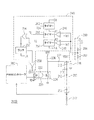
図3は、本発明第二の実施例によるバックライトモジュールの回路図である。図3において、バックライトモジュール300は、第一の実施例によって提供されるバックライトモジュール200Aと実質的には同様に、光源モジュール310、PWMコントローラ380、駆動モジュール320、変圧器330及び保護モジュール340を有する。当業者は、これらの手段の接続関係や動作原理を理解するために、第一の実施例における、光源モジュール210、PWMコントローラ280、駆動モジュール220、変圧器230及び保護モジュール240に関する説明を参照することができる。
FIG. 3 is a circuit diagram of a backlight module according to the second embodiment of the present invention. In FIG. 3, the
しかし、保護モジュール340には、高いヒステリシス値を有するヒステリシスコンパレータ342が第一の実施例におけるコンパレータ248の代わりに用いられる、という点で異なる。本実施例において、ヒステリシスコンパレータ342はまた、プリセット電圧Vr2を有する駆動電圧VOUTの検出信号を比較する。しかし、検出信号が(コンパレータ342の)ヒステリシス電圧だけプリセット電圧Vr2よりも大きい時、ヒステリシスコンパレータ342は高レベルの出力R3を発生する。したがって、本実施例において保護モジュール340は一つのタイマーの数を減らすことが可能である(すなわち、タイマー252は省くことができる)。
However, the protection module 340 is different in that a
検出信号が一つ以上のヒステリシス電圧だけプリセット電圧Vr2よりも大きい時、ヒステリシスコンパレータ342はORゲート344に高レベルの出力R3を発生する。ORゲート344の他の入力端はラッチ256の出力を受け取るために用いられる。このように、ヒステリシスコンパレータ342が高レベルの出力R3を発生するとき、出力R3はORゲート344を介してインバータ346に送られ、インバータ346によって反転された後にANDゲート222に低レベルのエラー信号E2を発生する。特に、ヒステリシスコンパレータ342の出力がラッチを通らないので、ヒステリシスコンパレータ342が低レベルの出力R3を再び出力する正常状態に駆動電圧VOUTの電圧が回復する限りにおいて、バックライトモジュール300は自動的に再起動され、ユーザーが手動でエラーリセット信号EAを有効にする必要はない。
When the detection signal is greater than the preset voltage Vr2 by one or more hysteresis voltages, the
図4は、本発明第三の実施例によるバックライトモジュールの回路図である。図4において、本実施例によって提供されるバックライトモジュール400は、第一の実施例によって提供されるバックライトモジュール200Aと概ね同じであり、光源モジュール410、PWMコントローラ480、駆動モジュール420、変圧器430及び保護モジュール440を有する。当業者は、これらの手段の接続関係や動作原理を理解するために、第一の実施例における光源モジュール210、PWMコントローラ280、駆動モジュール220、変圧器230及び保護モジュール240に関する説明を参照することができる。
FIG. 4 is a circuit diagram of a backlight module according to a third embodiment of the present invention. In FIG. 4, a
第一の実施例との違いは、バックライトモジュール400が調光機能を有するように、駆動モジュール420はさらに調光信号DIMを受け取る、ということである。本実施例において、駆動モジュール420はANDゲート222、NMOSトランジスタ224及びANDゲート422を備えている。ANDゲート422はエラーリセット信号EA及び調光信号DIMを受け取るために用いられる。調光信号DIMの周波数はPWM信号Vpwmのそれよりも低い。駆動モジュール420のオン−オフ切り替えは、光変調効果を達成するために調光信号DIMのデューティ・サイクルを制御することによって制御され得る。
The difference from the first embodiment is that the
図5は、本発明の好適な実施例による調光信号及びPWM信号のタイミングチャートである。図4及び図5を同時に参照すると、本実施例において光源モジュール410の輝度が低くされる必要があるとき、PWM信号Vpwmの周波数よりも相対的に低い周波数で調光信号DIM(図5に示されるように)をANDゲート422の入力端に送ることのみが必要とされる。それから、ANDゲート222はPWM信号Vpwm及び調光信号DIMのAND動作を実行することができる。このように、光源モジュール410の輝度を低くするように、K1信号はトランジスタ224のゲートに出力される。一方、光源モジュール410の輝度が上昇させられる必要があるときは、ANDゲート422の入力端に大きなデューティ・サイクルを有する調光信号DIMを発生することのみが必要とされる。
FIG. 5 is a timing chart of a dimming signal and a PWM signal according to a preferred embodiment of the present invention. Referring to FIGS. 4 and 5 at the same time, when the luminance of the
上述の観点において、本発明は少なくとも以下の利点を有する。 In view of the above, the present invention has at least the following advantages.
1.本発明が駆動電圧を発生するために変圧器を導入するので、本発明は光源を駆動するためにより多重な駆動電圧を提供し、本発明によって提供される駆動回路は、異なる大きさのバックライトモジュールにおいて用いられるのに適している。 1. Since the present invention introduces a transformer to generate the drive voltage, the present invention provides more multiple drive voltages to drive the light source, and the drive circuit provided by the present invention has different sized backlights Suitable for use in modules.
2.本発明が駆動電圧を発生するために変圧器を導入するので、本発明は、ブーストによってだけでなく、バック(降圧)によっても駆動電圧を発生することができるので、本発明はより柔軟に用いられる。 2. Since the present invention introduces a transformer to generate the drive voltage, the present invention can generate the drive voltage not only by boost but also by buck (step-down), so the present invention can be used more flexibly. It is done.
3.本発明が保護モジュールを有するので、保護モジュールは低すぎるあるいは高すぎる電圧下で、光源の動作を保護することができる。 3. Since the present invention has a protection module, the protection module can protect the operation of the light source under a voltage that is too low or too high.
4.本発明はまた、実用上の要求に応じてユーザーがバックライトモジュールの輝度を変調することができるように、調光機能を有することができる。 4). The present invention can also have a dimming function so that the user can modulate the brightness of the backlight module according to practical requirements.
本発明は好ましい実施例によって上述のように開示されたが、それらは本発明を限定することを意図しない。当業者の誰でも、本発明の精神と範囲から逸脱することなく、変更や改良をすることができる。したがって、発明の保護する範囲を添付の請求項に記載される。 While this invention has been disclosed above by the preferred embodiments, they are not intended to limit the invention. Anyone skilled in the art can make changes and modifications without departing from the spirit and scope of the present invention. Accordingly, the scope of protection of the invention is set forth in the appended claims.
VDD:電源
VOUT:駆動電圧
Vr1、Vr2:プリセット電圧
Vpwm:PWM信号
R1、R2:比較結果
E1、E2:エラー信号
DIM:調光信号
200A、300、400:バックライトモジュール
210、310、410:光源モジュール
212:LED
220、320、420:駆動モジュール
222、422:ANDゲート
224:NMOSトランジスタ
230、330、430:変圧器
232:一次コイル
234:二次コイル
240、340、440:保護モジュール
246、248:コンパレータ
250:初期タイマー
252:第1タイマー
256:ラッチ
254:ORゲート
258:インバータ
260:第2タイマー
280、380、480:PWMコントローラ
290:電圧検出モジュール
292、294:抵抗
VDD: power supply VOUT: drive voltage Vr1, Vr2: preset voltage Vpwm: PWM signal R1, R2: comparison result E1, E2: error signal DIM: dimming
220, 320, 420: drive
Claims (23)
一次コイル及び二次コイルを備えている変圧器と、
前記発光ダイオードの検出信号に応じてパルス幅変調(PWM)信号を発生するために用いられるPWMコントローラと、
前記変圧器の前記一次コイルの第二端に接続され、前記PWM信号に応じて前記変圧器に電力を送る駆動モジュールと、を備え、
前記一次コイルの第一端は電源に接続され、前記二次コイルの第一端は直列接続された前記発光ダイオードに接続され、前記二次コイルの第二端は接地されることを特徴とする駆動回路。 A drive circuit of a light emitting diode (LED);
A transformer comprising a primary coil and a secondary coil;
A PWM controller used to generate a pulse width modulation (PWM) signal in response to a detection signal of the light emitting diode;
A drive module connected to the second end of the primary coil of the transformer and sending power to the transformer in response to the PWM signal;
The first end of the primary coil is connected to a power source, the first end of the secondary coil is connected to the light emitting diodes connected in series, and the second end of the secondary coil is grounded. Driving circuit.
前記駆動モジュールは前記エラー信号に応じて前記変圧器に前記電力を送るのを停止することを特徴とする、請求項1に記載の発光ダイオードの駆動回路。 A protection module connected to the transformer and used to generate an error signal when the driving voltage output to the light emitting diode by the transformer is lower than a first voltage or higher than a second voltage; In addition,
The light emitting diode driving circuit according to claim 1, wherein the driving module stops sending the power to the transformer in response to the error signal.
前記PWM信号及び前記エラー信号を受け取るために用いられるANDゲートと、
前記ANDゲートの出力に接続されたゲート、前記一次コイルの前記第二端に接続されたドレイン及び接地されたソースを有するNMOSトランジスタと、を備えることを特徴とする、請求項2に記載の発光ダイオードの駆動回路。 The drive module is
An AND gate used to receive the PWM signal and the error signal;
The light emitting device of claim 2, further comprising: an NMOS transistor having a gate connected to an output of the AND gate, a drain connected to the second end of the primary coil, and a grounded source. Diode drive circuit.
前記調光信号の周波数は前記PWM信号の周波数とは異なることを特徴とする、請求項3に記載の発光ダイオードの駆動回路。 The driving module further receives a dimming signal that modulates the luminance of the light emitting diode,
4. The light emitting diode driving circuit according to claim 3, wherein the frequency of the dimming signal is different from the frequency of the PWM signal.
前記第一コンパレータは、前記駆動電圧が前記第一電圧より低いかどうかを決定し、第一比較結果を出力するために、電圧検出信号と第一プリセット電圧とを比較するために用いられ、
前記第一タイマーは、前記第一比較結果を受け取り、第一プリセットタイムの間に前記駆動電圧が前記第一プリセット電圧より低いとき、第一タイミング信号を発生し、
前記ラッチは、前記第一タイミング信号を受け取ることを特徴とする、請求項5に記載の発光ダイオードの駆動回路。 The protection module includes a first comparator, a first timer, and a latch,
The first comparator is used to determine whether the driving voltage is lower than the first voltage and compare a voltage detection signal with a first preset voltage to output a first comparison result;
The first timer receives the first comparison result, and generates a first timing signal when the driving voltage is lower than the first preset voltage during a first preset time,
The light emitting diode driving circuit according to claim 5, wherein the latch receives the first timing signal.
第二プリセットタイムの間に前記駆動電圧が前記第二電圧より大きいかどうかを決定し第二比較結果を出力するように電圧検出信号を第二プリセット電圧と比較するように用いられる第二コンパレータと、
前記第二比較結果を受け取り、第二プリセットタイムの間に前記駆動電圧が前記第二電圧より大きいとき、第二タイミング信号を発生させる第二タイマーと、
前記第一タイミング信号と前記第二タイミング信号とを受け取り、前記ラッチへ前記出力を送るORゲートと、を備えることを特徴とする、請求項6に記載の発光ダイオードの駆動回路。 The protection module is
A second comparator used to compare a voltage detection signal with a second preset voltage to determine whether the drive voltage is greater than the second voltage during a second preset time and to output a second comparison result; ,
A second timer that receives the second comparison result and generates a second timing signal when the drive voltage is greater than the second voltage during a second preset time;
The light emitting diode driving circuit according to claim 6, further comprising: an OR gate that receives the first timing signal and the second timing signal and sends the output to the latch.
前記ヒステリシス第二コンパレータは、前記電圧検出信号と第二プリセット電圧とを比較するように用いられ、前記比較結果に応じて第二タイミング信号を出力し、
前記ORゲートは、前記ラッチの出力信号と前記第二タイミング信号とを受け取ること、を特徴とする、請求項6に記載の発光ダイオードの駆動回路。 The protection module further comprises a hysteresis second comparator and an OR gate,
The hysteresis second comparator is used to compare the voltage detection signal and a second preset voltage, and outputs a second timing signal according to the comparison result,
The light emitting diode driving circuit according to claim 6, wherein the OR gate receives the output signal of the latch and the second timing signal.
前記インバータは、前記ラッチの出力を反転することによって前記エラー信号を発生するように用いられることを特徴とする、請求項6に記載の発光ダイオードの駆動回路。 The protection module further includes an inverter,
The light emitting diode driving circuit according to claim 6, wherein the inverter is used to generate the error signal by inverting the output of the latch.
前記インバータは、前記ORゲートの出力を反転した後に前記エラー信号を発生するように用いられることを特徴とする、請求項8に記載の発光ダイオードの駆動回路。 The protection module further includes an inverter,
The light emitting diode driving circuit according to claim 8, wherein the inverter is used to generate the error signal after inverting the output of the OR gate.
前記インバータは、前記ORゲートの出力を反転した後に前記エラー信号を発生させるように用いられることを特徴とする、請求項9に記載の発光ダイオードの駆動回路。 The protection module further includes an inverter,
The light emitting diode driving circuit according to claim 9, wherein the inverter is used to generate the error signal after inverting the output of the OR gate.
前記ブースターは、光源モジュールを駆動するDC駆動電圧を発生するように電源及び光源モジュールに接続され、
前記保護モジュールは、前記駆動電圧が第一プリセット電圧より大きいときにエラー信号を発生するためのブースターに接続され、
前記PWMコントローラは、前記光源モジュールの検出信号に応じてPWM信号を発生し、
前記駆動モジュールは、ANDゲート及びNMOSトランジスタを備え、
前記ANDゲートは、前記PWM信号及び前記エラー信号を受け取り、
前記NMOSトランジスタは、前記ANDゲートの出力に接続されたゲートと、前記ブースターに接続されたドレインと、接地されたソースとを備え、
前記駆動モジュールは、前記エラー信号に応じて前記光源モジュールに電力を出力することを停止すること、を特徴とする、バックライトモジュール。 A light source module, booster, protection module, PWM controller and drive module
The booster is connected to the power source and the light source module so as to generate a DC driving voltage for driving the light source module,
The protection module is connected to a booster for generating an error signal when the driving voltage is greater than a first preset voltage;
The PWM controller generates a PWM signal according to the detection signal of the light source module,
The driving module includes an AND gate and an NMOS transistor,
The AND gate receives the PWM signal and the error signal;
The NMOS transistor comprises a gate connected to the output of the AND gate, a drain connected to the booster, and a grounded source,
The drive module stops outputting power to the light source module in response to the error signal.
前記調光信号の周波数はPWM信号の周波数とは異なることを特徴とする、請求項13に記載のバックライトモジュール。 The drive module receives a dimming signal to dimm the brightness of the light source module;
The backlight module according to claim 13, wherein the frequency of the dimming signal is different from the frequency of the PWM signal.
前記保護モジュールは、前記電圧検出信号に応じて前記駆動電圧が前記第一プリセット電圧より大きいかどうかを決定する前記ブースターに接続されることを特徴とする、請求項13に記載のバックライトモジュール。 A voltage detection module that generates a voltage detection signal according to the driving voltage;
The backlight module of claim 13, wherein the protection module is connected to the booster that determines whether the driving voltage is greater than the first preset voltage in response to the voltage detection signal.
23. The back of claim 22, wherein the protection module further comprises a latch for latching the error signal for the predetermined period after the driving voltage becomes lower than the second preset voltage. Light module.
Applications Claiming Priority (1)
| Application Number | Priority Date | Filing Date | Title |
|---|---|---|---|
| TW095109796A TW200737066A (en) | 2006-03-22 | 2006-03-22 | Driving circuit with protection module for back light module |
Publications (1)
| Publication Number | Publication Date |
|---|---|
| JP2007258671A true JP2007258671A (en) | 2007-10-04 |
Family
ID=38532876
Family Applications (1)
| Application Number | Title | Priority Date | Filing Date |
|---|---|---|---|
| JP2006305705A Pending JP2007258671A (en) | 2006-03-22 | 2006-11-10 | Drive circuit of light-emitting diode |
Country Status (3)
| Country | Link |
|---|---|
| US (1) | US20070222739A1 (en) |
| JP (1) | JP2007258671A (en) |
| TW (1) | TW200737066A (en) |
Cited By (8)
| Publication number | Priority date | Publication date | Assignee | Title |
|---|---|---|---|---|
| JP2009104848A (en) * | 2007-10-22 | 2009-05-14 | Funai Electric Co Ltd | Backlight led drive circuit |
| JP2010176853A (en) * | 2009-01-27 | 2010-08-12 | Mitsubishi Electric Corp | Light emitting element lighting control device |
| JP2011146329A (en) * | 2010-01-18 | 2011-07-28 | Mitsubishi Electric Corp | Lighting device and illuminating device |
| KR101209905B1 (en) * | 2011-04-26 | 2012-12-20 | 주식회사이은 | LED Driving Circuit having possible output stabilecurrent high-voltage DC and LED lamp using the same |
| JPWO2011055533A1 (en) * | 2009-11-04 | 2013-03-28 | ローム株式会社 | Driving circuit and driving method for backlight LED string, and backlight and display device using the same |
| TWI410172B (en) * | 2009-04-16 | 2013-09-21 | Chunghwa Picture Tubes Ltd | Driving circuit of backlight module |
| JP2013235848A (en) * | 2013-07-23 | 2013-11-21 | Mitsubishi Electric Corp | Lighting device and illumination device |
| TWI495391B (en) * | 2012-08-03 | 2015-08-01 |
Families Citing this family (13)
| Publication number | Priority date | Publication date | Assignee | Title |
|---|---|---|---|---|
| CN101389177A (en) * | 2007-09-14 | 2009-03-18 | 群康科技(深圳)有限公司 | Light regulating circuit |
| CN101409047B (en) * | 2007-10-10 | 2010-09-29 | 群康科技(深圳)有限公司 | Backlight regulating circuit |
| AT12495U1 (en) * | 2010-10-08 | 2012-06-15 | Tridonic Ag | ERROR DETECTION FOR LUMINAIRE DIODES |
| KR101717565B1 (en) * | 2010-12-23 | 2017-03-17 | 삼성전자 주식회사 | Display apparatus and control method |
| KR101857806B1 (en) * | 2011-08-11 | 2018-05-14 | 엘지디스플레이 주식회사 | Liquid Crystal Display Device and Driving Method the same |
| FR2982115B1 (en) * | 2011-10-31 | 2014-09-26 | Fagorbrandt Sas | METHOD AND DEVICE FOR CONTROLLING THE LUMINOUS INTENSITY OF AN ILLUMINATION DEVICE, IN PARTICULAR FOR A HOOD |
| CN103065588B (en) * | 2012-12-14 | 2015-07-15 | 深圳市华星光电技术有限公司 | Light-emitting diode (LED) backlight drive circuit and liquid crystal display device |
| US9198254B2 (en) | 2012-12-14 | 2015-11-24 | Shenzhen China Star Optoelectronics Technology Co., Ltd | LED backlight driving circuit and LCD device |
| US9774257B2 (en) * | 2014-05-23 | 2017-09-26 | Allegro Microsystems, Llc | Control circuit for a switching regulator driving an LED load with controlled PWM dimming |
| JP2017021938A (en) * | 2015-07-08 | 2017-01-26 | パナソニックIpマネジメント株式会社 | Lighting control unit, lighting system, and facilities equipment |
| US10215795B1 (en) * | 2018-04-13 | 2019-02-26 | Infineon Technologies Ag | Three level gate monitoring |
| US11330687B2 (en) * | 2019-06-25 | 2022-05-10 | ERP Power, LLC | System and method for invalid pulse rejection |
| CN111583878B (en) * | 2020-06-11 | 2021-09-10 | 京东方科技集团股份有限公司 | Backlight source control device, control method and display device |
Citations (2)
| Publication number | Priority date | Publication date | Assignee | Title |
|---|---|---|---|---|
| JP2004319583A (en) * | 2003-04-11 | 2004-11-11 | Toritsu Tsushin Kogyo Kk | Led lighting system |
| JP2005286060A (en) * | 2004-03-29 | 2005-10-13 | Rohm Co Ltd | Laser element drive unit |
Family Cites Families (12)
| Publication number | Priority date | Publication date | Assignee | Title |
|---|---|---|---|---|
| US6388853B1 (en) * | 1999-09-28 | 2002-05-14 | Power Integrations, Inc. | Method and apparatus providing final test and trimming for a power supply controller |
| US7071762B2 (en) * | 2001-01-31 | 2006-07-04 | Koninklijke Philips Electronics N.V. | Supply assembly for a led lighting module |
| US7088334B2 (en) * | 2001-06-28 | 2006-08-08 | Matsushita Electric Industrial Co., Ltd. | Liquid crystal display device and manufacturing method thereof, and drive control method of lighting unit |
| EP1322139A1 (en) * | 2001-12-19 | 2003-06-25 | Toyoda Gosei Co., Ltd. | LED lamp apparatus for vehicles |
| EP1579735B1 (en) * | 2002-12-19 | 2016-03-09 | Koninklijke Philips N.V. | Leds driver |
| US20040125621A1 (en) * | 2002-12-30 | 2004-07-01 | Ta-Yung Yang | Synchronous rectifier of flyback power converter |
| JP2004276739A (en) * | 2003-03-14 | 2004-10-07 | Koito Mfg Co Ltd | Lighting equipment for vehicle |
| US6888383B1 (en) * | 2003-09-08 | 2005-05-03 | National Semiconductor Corporation | Open loop LED driver system |
| US6943504B1 (en) * | 2003-11-24 | 2005-09-13 | National Semiconductor Corporation | Open loop magnetic boost LED driver system and method |
| US7358706B2 (en) * | 2004-03-15 | 2008-04-15 | Philips Solid-State Lighting Solutions, Inc. | Power factor correction control methods and apparatus |
| JP2006221886A (en) * | 2005-02-09 | 2006-08-24 | Koito Mfg Co Ltd | Lighting control device of vehicular lamp tool |
| JP5025913B2 (en) * | 2005-05-13 | 2012-09-12 | シャープ株式会社 | LED drive circuit, LED illumination device, and backlight |
-
2006
- 2006-03-22 TW TW095109796A patent/TW200737066A/en unknown
- 2006-06-09 US US11/309,019 patent/US20070222739A1/en not_active Abandoned
- 2006-11-10 JP JP2006305705A patent/JP2007258671A/en active Pending
Patent Citations (2)
| Publication number | Priority date | Publication date | Assignee | Title |
|---|---|---|---|---|
| JP2004319583A (en) * | 2003-04-11 | 2004-11-11 | Toritsu Tsushin Kogyo Kk | Led lighting system |
| JP2005286060A (en) * | 2004-03-29 | 2005-10-13 | Rohm Co Ltd | Laser element drive unit |
Cited By (8)
| Publication number | Priority date | Publication date | Assignee | Title |
|---|---|---|---|---|
| JP2009104848A (en) * | 2007-10-22 | 2009-05-14 | Funai Electric Co Ltd | Backlight led drive circuit |
| JP2010176853A (en) * | 2009-01-27 | 2010-08-12 | Mitsubishi Electric Corp | Light emitting element lighting control device |
| TWI410172B (en) * | 2009-04-16 | 2013-09-21 | Chunghwa Picture Tubes Ltd | Driving circuit of backlight module |
| JPWO2011055533A1 (en) * | 2009-11-04 | 2013-03-28 | ローム株式会社 | Driving circuit and driving method for backlight LED string, and backlight and display device using the same |
| JP2011146329A (en) * | 2010-01-18 | 2011-07-28 | Mitsubishi Electric Corp | Lighting device and illuminating device |
| KR101209905B1 (en) * | 2011-04-26 | 2012-12-20 | 주식회사이은 | LED Driving Circuit having possible output stabilecurrent high-voltage DC and LED lamp using the same |
| TWI495391B (en) * | 2012-08-03 | 2015-08-01 | ||
| JP2013235848A (en) * | 2013-07-23 | 2013-11-21 | Mitsubishi Electric Corp | Lighting device and illumination device |
Also Published As
| Publication number | Publication date |
|---|---|
| TW200737066A (en) | 2007-10-01 |
| US20070222739A1 (en) | 2007-09-27 |
Similar Documents
| Publication | Publication Date | Title |
|---|---|---|
| JP2007258671A (en) | Drive circuit of light-emitting diode | |
| US8274237B2 (en) | LED driver circuit with over-current protection during a short circuit condition | |
| US10298014B2 (en) | System and method for controlling solid state lamps | |
| KR101910669B1 (en) | Control circuit of switching power supply for driving light emitting elements, and light emitting device and electronic apparatus using the same | |
| JP5829067B2 (en) | LED driving device, lighting device, liquid crystal display device | |
| US8044604B2 (en) | Inverter | |
| JP4975856B2 (en) | Integrated circuit for lighting device and lighting device | |
| JP5848898B2 (en) | Load driving circuit and light emitting device and display device using the same | |
| WO2012127844A1 (en) | Switching power source control circuit for driving light-emitting element, and light-emitting device and electronic apparatus using same | |
| JP2013021117A (en) | Led drive device, luminaire, and liquid crystal display device | |
| JP2011522435A (en) | LED lamp driver and method of driving | |
| US20130038819A1 (en) | Driving circuit for light emitting element, light emitting device using same, and display apparatus | |
| CN100463580C (en) | Driving circuit of backlight device with the protection module group | |
| KR101510359B1 (en) | Light emitting diode luminance system having clamping device | |
| JP2006278526A (en) | Light emitting diode driving device | |
| WO2017033629A1 (en) | Light-emitting element drive device | |
| TW200816127A (en) | Lighting apparatus and driving circuit thereof | |
| JP5735832B2 (en) | Control circuit for switching power supply for driving light emitting element, light emitting device and electronic device | |
| JP2013109921A (en) | Drive circuit for light-emitting element, and light-emitting device and electronic equipment using the same | |
| TW201705664A (en) | Boost apparatus with integration of OCP detection and OVP detection | |
| JP6247455B2 (en) | LIGHT EMITTING ELEMENT DRIVE CIRCUIT, AND LIGHT EMITTING DEVICE AND ELECTRONIC DEVICE USING THE SAME | |
| JP5698579B2 (en) | Control circuit for switching power supply for driving light emitting element, and light emitting device and electronic apparatus using them | |
| JP5850612B2 (en) | LIGHT EMITTING ELEMENT DRIVE CIRCUIT, AND LIGHT EMITTING DEVICE AND ELECTRONIC DEVICE | |
| JP5054236B1 (en) | LED lighting device | |
| JP7258662B2 (en) | LED driving device, display device, and control device for LED driving device |
Legal Events
| Date | Code | Title | Description |
|---|---|---|---|
| A977 | Report on retrieval |
Free format text: JAPANESE INTERMEDIATE CODE: A971007 Effective date: 20100419 |
|
| A131 | Notification of reasons for refusal |
Free format text: JAPANESE INTERMEDIATE CODE: A131 Effective date: 20100427 |
|
| A02 | Decision of refusal |
Free format text: JAPANESE INTERMEDIATE CODE: A02 Effective date: 20101005 |