JP2007258385A - Heat-sink device - Google Patents
Heat-sink device Download PDFInfo
- Publication number
- JP2007258385A JP2007258385A JP2006079854A JP2006079854A JP2007258385A JP 2007258385 A JP2007258385 A JP 2007258385A JP 2006079854 A JP2006079854 A JP 2006079854A JP 2006079854 A JP2006079854 A JP 2006079854A JP 2007258385 A JP2007258385 A JP 2007258385A
- Authority
- JP
- Japan
- Prior art keywords
- mounting
- heat sink
- sink device
- pattern
- stud
- Prior art date
- Legal status (The legal status is an assumption and is not a legal conclusion. Google has not performed a legal analysis and makes no representation as to the accuracy of the status listed.)
- Pending
Links
Images


Abstract
Description
本発明は、放熱性能が向上され、外来ノイズ/放射ノイズを減衰することができるヒートシンク装置に関するものである。 The present invention relates to a heat sink device having improved heat dissipation performance and capable of attenuating external noise / radiated noise.
に関連する先行技術文献としては次のようなものがある。 There are the following prior art documents related to.
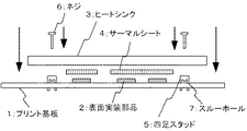
図8は従来より一般に使用されている従来例の構成説明図で、図9は図8の要部組立説明図である。
図において、プリント基板1には、表面実装部品2が取付けられている。
ヒートシンク3は、サーマルシート4を介して表面実装部品2に接触している。
そして、ヒートシンク3は、プリント基板1に四足スタッド5とネジ6により支持されている。
FIG. 8 is an explanatory diagram of a configuration of a conventional example that is generally used conventionally, and FIG. 9 is an explanatory diagram of an essential part assembly of FIG.
In the figure, a surface mount component 2 is attached to a printed circuit board 1.
The heat sink 3 is in contact with the surface-mounted component 2 through the thermal sheet 4.
The heat sink 3 is supported on the printed circuit board 1 by quadruped studs 5 and screws 6.
以上の構成において、図9に示す如く、まず、プリント基板1に表面実装部品2が取り付けられる。
プリント基板1のスルーホール7に四足スタッド5が取り付けられ、次に、表面実装部品2にサーマルシート4が取付けられ、ヒートシンク3が四足スタッド5にネジ6により取り付けられる。
In the above configuration, the surface mount component 2 is first attached to the printed circuit board 1 as shown in FIG.
The quadruped stud 5 is attached to the through hole 7 of the printed circuit board 1, the thermal sheet 4 is then attached to the surface mount component 2, and the heat sink 3 is attached to the quadruped stud 5 with screws 6.
このような装置においては、以下の間題点がある。
市販品である四足スタッド5の高さは一般に低く、四足スタッド5の高さの制約により、ネジ6がプリント基板1に突き当たらないようにするために、ネジ6の長さが必然的に短くなり、ヒートシンク3の実装高さに自由度が無い。
全体の高さを低くするためには四足スタッド5を低くして対応することができるが、ネジ6の長さが長い場合には、ネジ6を貫通させる穴をプリント基板1に設ける必要性がある。
Such an apparatus has the following problems.
The height of the commercially available quadruped stud 5 is generally low, and the length of the screw 6 is inevitable to prevent the screw 6 from striking the printed circuit board 1 due to the height restriction of the quadruped stud 5. The mounting height of the heat sink 3 is not flexible.
In order to reduce the overall height, the quadruple stud 5 can be lowered, but if the length of the screw 6 is long, it is necessary to provide a hole in the printed circuit board 1 through which the screw 6 passes. There is.
四足スタッド5のネジ穴に対応してプリント基板1にネジ6を通すための貫通穴を設けると、四足スタッド5の四つの足の穴の中央に貫通穴が開き、プリント基板1の強度が弱くなる。このため、ヒートシンク3の実装高さを低くするには限界が生ずる。 If a through hole for passing the screw 6 through the printed circuit board 1 corresponding to the screw hole of the quadruped stud 5 is provided, a through hole is opened at the center of the four foot holes of the quadruped stud 5, and the strength of the printed circuit board 1 is increased. Becomes weaker. For this reason, there is a limit in reducing the mounting height of the heat sink 3.
放熱のための伝熱の場所が表面実装部品2と接触している部分に限られる(表面実装部品2表面からのみ放熱可能)。内層パターンを四足スタッド5の足が半田付けされているスルーホールに接続することはできるが、四足スタッド5の足は細いので、接触面積が小さい。
四足スタッド5の形状により、四足スタッド5の実装面積が大きくなり、高密度実装に不向きである。
The place of heat transfer for heat radiation is limited to the portion in contact with the surface mount component 2 (heat can be radiated only from the surface of the surface mount component 2). Although the inner layer pattern can be connected to the through-hole in which the legs of the quadruped stud 5 are soldered, the leg of the quadruped stud 5 is thin, so the contact area is small.
Due to the shape of the quadruped stud 5, the mounting area of the quadruped stud 5 is large, which is not suitable for high-density mounting.
本発明の目的は、上記の課題を解決するもので、
表面実装部品そのものの放熱だけでなく、プリント基板の内層にこもる熱も同時に放熱する。
内層パターンとヒートシンクを電気的に接続することにより、プリント基板全体の温度を均衡化し、プリント基板全体の温度を下げ、局所的な高温部ができないようにする。
ノイズの空間伝播の抑制を図る。
以上の如きヒートシンク装置を提供することにある。
The object of the present invention is to solve the above problems.
In addition to the heat dissipation of the surface mount component itself, the heat trapped in the inner layer of the printed circuit board is also released.
By electrically connecting the inner layer pattern and the heat sink, the temperature of the entire printed circuit board is balanced, the temperature of the entire printed circuit board is lowered, and a local high temperature portion is not formed.
Suppresses the spatial propagation of noise.
An object of the present invention is to provide a heat sink device as described above.
このような課題を達成するために、本発明では、請求項1のヒートシンク装置においては、
内層パターンを有する多層プリント基板が取り付けられるヒートシンク装置において、前記多層プリント基板に設けられ所定の内層パターンと電気的に接続されスルーホール状をなす取付けパターンと、この取付けパターンに一端側が挿入固定され金属材よりなる取付けスタッドと、この取付けスタッドの他端にヒートシンクを着脱自在に取付ける取付手段とを具備したことを特徴とする。
In order to achieve such a subject, in the present invention, in the heat sink device of claim 1,
In a heat sink device to which a multilayer printed board having an inner layer pattern is attached, a mounting pattern that is provided on the multilayer printed board and is electrically connected to a predetermined inner layer pattern to form a through hole, and one end side of which is inserted and fixed to the mounting pattern is a metal It is characterized by comprising a mounting stud made of a material and mounting means for detachably mounting a heat sink to the other end of the mounting stud.
本発明の請求項2のヒートシンク装置においては、請求項1記載のヒートシンク装置において、
前記取付けスタッドは、取付けパターンへの挿入側が小さな外形を有する段部を有することを特徴とする。
In the heat sink device according to claim 2 of the present invention, in the heat sink device according to claim 1,
The mounting stud has a step portion having a small outer shape on an insertion side to the mounting pattern.
本発明の請求項3のヒートシンク装置においては、請求項1又は請求項2記載のヒートシンク装置において、
前記取付けスタッドの段部が前記取付けパターンに半田付け固定されたことを特徴とする。
In the heat sink device according to claim 3 of the present invention, in the heat sink device according to claim 1 or 2,
The step portion of the mounting stud is fixed by soldering to the mounting pattern.
本発明の請求項4のヒートシンク装置においては、請求項1乃至請求項3の何れかに記載のヒートシンク装置において、
前記ヒートシンクに設けられヒートシンクと前記所定の内層パターンと共に所定箇所にシールド室を構成するシールド板を具備したことを特徴とする。
In the heat sink device according to claim 4 of the present invention, in the heat sink device according to any one of claims 1 to 3,
A shield plate which is provided on the heat sink and forms a shield chamber at a predetermined location together with the heat sink and the predetermined inner layer pattern is provided.
本発明の請求項5のヒートシンク装置においては、請求項1乃至請求項4の何れかに記載のヒートシンク装置において、
前記取付手段は、前記取付けスタッドに設けられた雌ネジと、この雌ネジに取り付けられるネジとを具備したことを特徴とする。
In the heat sink device according to claim 5 of the present invention, in the heat sink device according to any one of claims 1 to 4,
The attachment means includes a female screw provided on the mounting stud and a screw attached to the female screw.
本発明の請求項6のヒートシンク装置においては、請求項1乃至請求項5の何れかに記載のヒートシンク装置において、
取付けパターンのパッド径と取付けスタッドの直径がほぼ等しくされたことを特徴とする。
In the heat sink device according to claim 6 of the present invention, in the heat sink device according to any one of claims 1 to 5,
The pad diameter of the mounting pattern is substantially equal to the diameter of the mounting stud.
本発明の請求項1によれば、次のような効果がある。
プリント基板の内層パターンと取付けパターンと取付けスタッドとヒートシンクが接続されるので、プリント基板の内層パターンの熱をヒートシンクに放熱することができ、プリント基板全体の温度を均衡化し、プリント基板全体の温度を下げ、局所的な高温部ができないようにできるヒートシンク装置が得られる。
According to claim 1 of the present invention, there are the following effects.
Since the printed circuit board inner layer pattern, mounting pattern, mounting stud and heat sink are connected, the heat of the printed circuit board inner layer pattern can be dissipated to the heat sink, and the temperature of the entire printed circuit board is balanced, A heat sink device can be obtained that can be lowered to prevent the formation of local high temperature portions.
内層のパターンに共通電位(グラウンド)を用いることにより、内層パターン/取付けパターン/取付けスタッド/ヒートシンクを共通の電位とすることができるので、静電シールド/電磁シールドが可能となり、外来ノイズ/放射ノイズを減衰することができるヒートシンク装置が得られる。 By using a common potential (ground) for the inner layer pattern, the inner layer pattern / mounting pattern / mounting stud / heat sink can be set at a common potential, enabling electrostatic shielding / electromagnetic shielding, and external noise / radiation noise. A heat sink device can be obtained.
取付けパターンに一端側が挿入固定され金属材よりなる取付けスタッドが設けられたので、内層パターンと取付けパターンの金属部と取付けスタッドとの接触面積が大きく得られ、接合強度が強く放熱効果が大きいヒートシンク装置が得られる。
取付けスタッドの高さを変更することにより、ヒートシンクの実装高さの制限が無いヒートシンク装置が得られる。
A mounting stud made of a metal material with one end inserted and fixed to the mounting pattern is provided, so that a large contact area between the inner layer pattern, the metal part of the mounting pattern, and the mounting stud can be obtained, and the joint strength is high and the heat dissipation effect is large. Is obtained.
By changing the height of the mounting stud, it is possible to obtain a heat sink device that does not limit the mounting height of the heat sink.
ヒートシンクを着脱自在に取付ける取付手段が設けられたので、取付けスタッドのみプリント基板に取り付ければ良く、半田付け作業等の熱容量の問題に基づく、ヒートシンクの形状に制限を受ける恐れが無い。また、半田付け後にヒートシンクを実装できるので、大きなヒートシンクの取り付けも可能なヒートシンク装置が得られる。
ヒートシンクには取り付け用の穴さえ空いていれば良いので、複雑な金属加工が不要となりヒートシンクを安価に作成できるヒートシンク装置が得られる。
Since the attachment means for detachably attaching the heat sink is provided, only the attachment stud need be attached to the printed circuit board, and there is no fear of being limited by the shape of the heat sink based on the problem of heat capacity such as soldering work. Further, since the heat sink can be mounted after soldering, a heat sink device capable of attaching a large heat sink can be obtained.
Since the heat sink only needs to have a hole for mounting, complicated metal processing is not required, and a heat sink device can be obtained that can be manufactured at low cost.
本発明の請求項2によれば、次のような効果がある。
取付けスタッドは、取付けパターンへの挿入側が小さな外形を有する段部を有するので、固定が容易なヒートシンク装置が得られる。
According to claim 2 of the present invention, there are the following effects.
Since the mounting stud has a step portion having a small outer shape on the insertion side to the mounting pattern, a heat sink device that can be easily fixed is obtained.
本発明の請求項3によれば、次のような効果がある。
取付けスタッドの段部が取付けパターンに半田付け固定されたので、クリーム半田等が使用でき組み立て固定が容易なヒートシンク装置が得られる。
According to claim 3 of the present invention, there are the following effects.
Since the stepped portion of the mounting stud is soldered and fixed to the mounting pattern, a heat sink device that can use cream solder or the like and can be easily assembled and fixed is obtained.
本発明の請求項4によれば、次のような効果がある。
ヒートシンクに設けられヒートシンクと内層パターンと共に所定箇所にシールド室を構成するシールド板が設けられたので、必要箇所のみのシールドが可能なヒートシンク装置が得られる。
According to claim 4 of the present invention, there are the following effects.
Since the shield plate which is provided on the heat sink and forms the shield chamber is provided at a predetermined location together with the heat sink and the inner layer pattern, a heat sink device capable of shielding only a necessary location can be obtained.
本発明の請求項5によれば、次のような効果がある。
取付手段は、取付けスタッドに設けられた雌ネジと、この雌ネジに取り付けられるネジとが設けられたので、ネジの締め付け具合により、ヒートシンクの実装高さを容易に変更できるヒートシンク装置が得られる。
According to claim 5 of the present invention, there are the following effects.
Since the attachment means is provided with a female screw provided on the attachment stud and a screw attached to the female screw, a heat sink device can be obtained in which the mounting height of the heat sink can be easily changed by the tightening condition of the screw.
本発明の請求項6によれば、次のような効果がある。
取付けパターンのパッド径と取付けスタッドの直径がほぼ等しくされたので、省スペースにでき、実装密度を上げることができるヒートシンク装置が得られる。
According to claim 6 of the present invention, there are the following effects.
Since the pad diameter of the mounting pattern is substantially equal to the diameter of the mounting stud, it is possible to obtain a heat sink device that can save space and increase the mounting density.
以下本発明を図面を用いて詳細に説明する。
図1は本発明の一実施例の要部構成説明図、図2は図1の要部構成説明図、図3は図1の組立説明図である。
図において、図8と同一記号の構成は同一機能を表す。
以下、図8との相違部分のみ説明する。
Hereinafter, the present invention will be described in detail with reference to the drawings.
FIG. 1 is an explanatory diagram of the main part configuration of one embodiment of the present invention, FIG. 2 is an explanatory diagram of the main part configuration of FIG. 1, and FIG.
In the figure, the same symbols as those in FIG. 8 represent the same functions.
Only the difference from FIG. 8 will be described below.
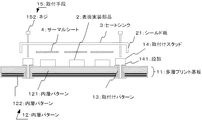
図1において、11は内層パターン12を有する多層プリント基板である。
取付けパターン13は、図2に示す如く、多層プリント基板11に設けられ所定の内層パターン12と電気的に接続されスルーホール状をなす。
この場合は、121は、取付けパターン13との電気的接続がある内層パターンで、グラウンド内層パターンが使用されている。122は、取付けパターン13との電気的接続が無い内層パターンである。
In FIG. 1, reference numeral 11 denotes a multilayer printed board having an inner layer pattern 12.
As shown in FIG. 2, the attachment pattern 13 is provided on the multilayer printed board 11 and is electrically connected to a predetermined inner layer pattern 12 to form a through hole.
In this case, 121 is an inner layer pattern having an electrical connection with the attachment pattern 13, and a ground inner layer pattern is used. Reference numeral 122 denotes an inner layer pattern that is not electrically connected to the attachment pattern 13.
この場合は、多層プリント基板11の内層に基準電位(グラウンド)となる内層パターン121を用意し、そのパターンになるべく大きな電流が流れるよう回路配線を行う。
取付けスタッド14は、取付けパターン13に一端側が挿入固定され金属材よりなる。
この場合は、取付けスタッド14は、取付けパターン13への挿入側が小さな外形を有する段部141を有する。
In this case, an inner layer pattern 121 serving as a reference potential (ground) is prepared in the inner layer of the multilayer printed board 11, and circuit wiring is performed so that as much current as possible flows through the pattern.
One end of the mounting stud 14 is inserted and fixed to the mounting pattern 13 and is made of a metal material.
In this case, the mounting stud 14 has a stepped portion 141 having a small outer shape on the insertion side to the mounting pattern 13.
そして、この場合は、取付けスタッドの段部141が、取付けパターン13に半田付け固定されている。
取付手段15は、取付けスタッド14の他端にヒートシンク16を着脱自在に取付ける。
この場合は、取付手段15は、取付けスタッドに設けられた雌ネジ151と、雌ネジ151に取り付けられるネジ152とを有する
また、取付けパターン13のパッド径と取付けスタッドの直径がほぼ等しくされている。
In this case, the step portion 141 of the mounting stud is fixed to the mounting pattern 13 by soldering.
The attachment means 15 removably attaches the heat sink 16 to the other end of the attachment stud 14.
In this case, the attachment means 15 includes a female screw 151 provided on the attachment stud and a screw 152 attached to the female screw 151. The pad diameter of the attachment pattern 13 and the diameter of the attachment stud are substantially equal. .
以上の構成において、図3に示す如く、取付けパターン13が設けられた、多層プリント基板11に表面実装部品2と取付けスタッド14とが取り付けられる。
次に、表面実装部品2にサーマルシート4が取付けられ、ヒートシンク3が取付けスタッド14にネジ152により取り付けられる。
In the above configuration, as shown in FIG. 3, the surface-mounted component 2 and the mounting stud 14 are attached to the multilayer printed board 11 provided with the mounting pattern 13.
Next, the thermal sheet 4 is attached to the surface mount component 2, and the heat sink 3 is attached to the attachment stud 14 with screws 152.
この結果、
プリント基板11の内層パターン121と取付けパターン13と取付けスタッド14とヒートシンク16が接続されるので、プリント基板11の内層パターン12の熱をヒートシンク16に放熱することができ、プリント基板11全体の温度を均衡化し、プリント基板11全体の温度を下げ、局所的な高温部ができないようにできるヒートシンク装置が得られる。
As a result,
Since the inner layer pattern 121, the mounting pattern 13, the mounting stud 14, and the heat sink 16 of the printed board 11 are connected, the heat of the inner layer pattern 12 of the printed board 11 can be radiated to the heat sink 16, and the temperature of the entire printed board 11 can be reduced. It is possible to obtain a heat sink device that can be balanced to lower the temperature of the entire printed circuit board 11 so that local high temperature portions are not generated.
内層のパターン121に共通電位(グラウンド)を用いることにより、内層パターン121/取付けパターン13/取付けスタッド14/ヒートシンク16を共通の電位とすることができるので、静電シールド/電磁シールドが可能となり、外来ノイズ/放射ノイズを減衰することができるヒートシンク装置が得られる。 By using a common potential (ground) for the inner layer pattern 121, the inner layer pattern 121 / mounting pattern 13 / mounting stud 14 / heat sink 16 can be set at a common potential, so that electrostatic shielding / electromagnetic shielding becomes possible. A heat sink device capable of attenuating external noise / radiated noise is obtained.
取付けパターン13に一端側が挿入固定され金属材よりなる取付けスタッド14が設けられたので、内層パターン121と取付けパターン13の金属部と取付けスタッド14との接触面積が大きく得られ、接合強度が強く放熱効果が大きいヒートシンク装置が得られる。
取付けスタッド14の高さを変更することにより、ヒートシンク16の実装高さの制限が無いヒートシンク装置が得られる。
Since the mounting pattern 14 is provided with a mounting stud 14 made of a metal material with one end being inserted and fixed, a large contact area between the inner layer pattern 121, the metal portion of the mounting pattern 13 and the mounting stud 14 is obtained, and the bonding strength is strong and heat dissipation. A heat sink device having a large effect can be obtained.
By changing the height of the mounting stud 14, a heat sink device that does not limit the mounting height of the heat sink 16 can be obtained.
ヒートシンク16を着脱自在に取付ける取付手段15が設けられたので、取付けスタッド14のみプリント基板11に取り付ければ良く、半田付け作業等の熱容量の問題に基づく、ヒートシンク16の形状に制限を受ける恐れが無い。また、半田付け後にヒートシンク16を実装できるので、大きなヒートシンク16の取り付けも可能なヒートシンク装置が得られる。
ヒートシンク16には取り付け用の穴さえ空いていれば良いので、複雑な金属加工が不要となりヒートシンク16を安価に作成できるヒートシンク装置が得られる。
Since the attachment means 15 for detachably attaching the heat sink 16 is provided, only the attachment stud 14 needs to be attached to the printed circuit board 11, and there is no risk of being restricted by the shape of the heat sink 16 based on the problem of heat capacity such as soldering work. . Further, since the heat sink 16 can be mounted after soldering, a heat sink device capable of mounting a large heat sink 16 can be obtained.
Since the heat sink 16 only needs to have a mounting hole, complicated metal processing is not required, and a heat sink device capable of producing the heat sink 16 at low cost can be obtained.
取付けスタッド14は、取付けパターン13への挿入側が小さな外形を有する段部141を有するので、固定が容易なヒートシンク装置が得られる。 Since the mounting stud 14 has a stepped portion 141 having a small outer shape on the insertion side to the mounting pattern 13, a heat sink device that can be easily fixed is obtained.
取付けスタッドの段部141が取付けパターン13に半田付け固定されたので、クリーム半田等が使用でき組み立て固定が容易なヒートシンク装置が得られる。 Since the step portion 141 of the mounting stud is fixed by soldering to the mounting pattern 13, a heat sink device which can use cream solder or the like and can be easily assembled and fixed is obtained.
取付手段15は、取付けスタッドに設けられた雌ネジ151と、この雌ネジ151に取り付けられるネジ152とが設けられたので、ネジ151の締め付け具合により、ヒートシンク16の実装高さを容易に変更できるヒートシンク装置が得られる。 Since the attachment means 15 is provided with the female screw 151 provided on the attachment stud and the screw 152 attached to the female screw 151, the mounting height of the heat sink 16 can be easily changed by the tightening condition of the screw 151. A heat sink device is obtained.
取付けパターン13のパッド径と取付けスタッド14の外形直径がほぼ等しくされたので、省スペースにでき、実装密度を上げることができるヒートシンク装置が得られる。 Since the pad diameter of the mounting pattern 13 and the outer diameter of the mounting stud 14 are substantially equal, a heat sink device that can save space and increase the mounting density can be obtained.
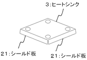
図4は本発明の他の実施例の要部構成説明図、図5は図4の要部部品図、図6に図4の組立図である。
図4において、シールド板21は、図5に示す如く、ヒートシンク16に設けられ、ヒートシンク16と所定の内層パターン121と共に、所定箇所にシールド室を構成する。
FIG. 4 is an explanatory view of the main part configuration of another embodiment of the present invention, FIG. 5 is a part diagram of the main part of FIG. 4, and FIG.
4, the shield plate 21 is provided on the heat sink 16 as shown in FIG. 5, and together with the heat sink 16 and the predetermined inner layer pattern 121, constitutes a shield chamber at a predetermined location.
この場合は、ヒートシンク16と始めから一体構成に作られており、表面実装部品2全体を覆っている。
図4においては、斜線部分がグラウンド電位となる。プリント基板11の所定部分を、確実にシールドすることができるヒートシンク装置が得られる。
図6に図4の組立図を示す。
In this case, the heat sink 16 and the heat sink 16 are integrally formed from the beginning and cover the entire surface mount component 2.
In FIG. 4, the shaded area is the ground potential. A heat sink device capable of reliably shielding a predetermined portion of the printed circuit board 11 is obtained.
FIG. 6 is an assembly view of FIG.
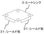
図7は本発明の他の実施例の要部構成説明図である。
本実施例においては、シールド板31は、ヒートシンク16に部分的に設けられたものである。
この結果、必要箇所のみのシールドが可能なヒートシンク装置が得られる。
FIG. 7 is an explanatory view showing the configuration of the main part of another embodiment of the present invention.
In this embodiment, the shield plate 31 is partially provided on the heat sink 16.
As a result, a heat sink device capable of shielding only necessary portions can be obtained.
なお、サーマルシート4にシールド効果のあるものを採用することにより、ノイズの空間伝播の抑制をより確実にできるヒートシンク装置が得られる。 In addition, by adopting a thermal sheet 4 having a shielding effect, a heat sink device can be obtained that can more reliably suppress noise spatial propagation.
なお、以上の説明は、本発明の説明および例示を目的として特定の好適な実施例を示したに過ぎない。
したがって本発明は、上記実施例に限定されることなく、その本質から逸脱しない範囲で更に多くの変更、変形をも含むものである。
The above description merely shows a specific preferred embodiment for the purpose of explanation and illustration of the present invention.
Therefore, the present invention is not limited to the above-described embodiments, and includes many changes and modifications without departing from the essence thereof.
1 プリント基板
2 表面実装部品
3 ヒートシンク
4 サーマルシート
5 四足スタッド
6 ネジ
7 スルーホール
11 多層プリント基板
12 内層パターン
121 内層パターン
122 内層パターン
13 取付けパターン
14 取付けスタッド
141 段部
15 取付手段
151 雌ネジ
152 ネジ
21 シールド板
31 シールド板
DESCRIPTION OF SYMBOLS 1 Printed circuit board 2 Surface mount component 3 Heat sink 4 Thermal sheet 5 Four leg stud 6 Screw 7 Through hole 11 Multilayer printed circuit board 12 Inner layer pattern 121 Inner layer pattern 122 Inner layer pattern 13 Mounting pattern 14 Mounting stud 141 Step part 15 Mounting means 151 Female screw 152 Screw 21 Shield plate 31 Shield plate
Claims (6)
前記多層プリント基板に設けられ所定の内層パターンと電気的に接続されスルーホール状をなす取付けパターンと、
この取付けパターンに一端側が挿入固定され金属材よりなる取付けスタッドと、
この取付けスタッドの他端にヒートシンクを着脱自在に取付ける取付手段と
を具備したことを特徴とするヒートシンク装置。 In a heat sink device to which a multilayer printed board having an inner layer pattern is attached,
A mounting pattern provided on the multilayer printed circuit board and electrically connected to a predetermined inner layer pattern to form a through hole;
A mounting stud made of a metal material with one end inserted and fixed to this mounting pattern;
And a mounting means for detachably mounting the heat sink to the other end of the mounting stud.
を特徴とする請求項1記載のヒートシンク装置。 The heat sink device according to claim 1, wherein the mounting stud has a step portion having a small outer shape on an insertion side to the mounting pattern.
を特徴とする請求項1又は請求項2記載のヒートシンク装置。 The heat sink device according to claim 1 or 2, wherein a step portion of the mounting stud is fixed to the mounting pattern by soldering.
を具備したことを特徴とする請求項1乃至請求項3の何れかに記載のヒートシンク装置。 4. The heat sink device according to claim 1, further comprising: a shield plate that is provided on the heat sink and forms a shield chamber at a predetermined location together with the heat sink and the predetermined inner layer pattern. 5.
この雌ネジに取り付けられるネジと
を具備したことを特徴とする請求項1乃至請求項4の何れかに記載のヒートシンク装置。 The mounting means includes a female screw provided on the mounting stud,
The heat sink device according to any one of claims 1 to 4, further comprising a screw attached to the female screw.
を特徴とする請求項1乃至請求項5の何れかに記載のヒートシンク装置。
6. The heat sink device according to claim 1, wherein the pad diameter of the mounting pattern and the diameter of the mounting stud are substantially equal.
Priority Applications (1)
| Application Number | Priority Date | Filing Date | Title |
|---|---|---|---|
| JP2006079854A JP2007258385A (en) | 2006-03-23 | 2006-03-23 | Heat-sink device |
Applications Claiming Priority (1)
| Application Number | Priority Date | Filing Date | Title |
|---|---|---|---|
| JP2006079854A JP2007258385A (en) | 2006-03-23 | 2006-03-23 | Heat-sink device |
Publications (1)
| Publication Number | Publication Date |
|---|---|
| JP2007258385A true JP2007258385A (en) | 2007-10-04 |
Family
ID=38632327
Family Applications (1)
| Application Number | Title | Priority Date | Filing Date |
|---|---|---|---|
| JP2006079854A Pending JP2007258385A (en) | 2006-03-23 | 2006-03-23 | Heat-sink device |
Country Status (1)
| Country | Link |
|---|---|
| JP (1) | JP2007258385A (en) |
Cited By (2)
| Publication number | Priority date | Publication date | Assignee | Title |
|---|---|---|---|---|
| JP2016512652A (en) * | 2013-02-28 | 2016-04-28 | ローレンス リバモア ナショナル セキュリティー, エルエルシー | Compact high current high efficiency laser diode driver |
| US9629282B2 (en) | 2011-06-10 | 2017-04-18 | Nec Corporation | Electronic device, structure, and heat sink |
Citations (7)
| Publication number | Priority date | Publication date | Assignee | Title |
|---|---|---|---|---|
| JPS62184798U (en) * | 1986-05-16 | 1987-11-24 | ||
| JPH08116195A (en) * | 1994-10-14 | 1996-05-07 | Matsushita Electric Ind Co Ltd | Shielding device for circuit unit |
| JPH0917921A (en) * | 1995-07-03 | 1997-01-17 | Yaskawa Electric Corp | Cooling structure of electronic device unit |
| JPH09116195A (en) * | 1995-10-23 | 1997-05-02 | Sony Corp | Infrared ray radiator |
| JP2000286587A (en) * | 1999-03-30 | 2000-10-13 | Matsushita Electric Ind Co Ltd | Electromagnetic shield structure at connector part with external cable |
| JP2004172459A (en) * | 2002-11-21 | 2004-06-17 | Advics:Kk | Heat dissipation structure of electronic component in electronic controller |
| JP2005294528A (en) * | 2004-03-31 | 2005-10-20 | Seiko Epson Corp | Circuit substrate and reducing method of noise therein |
-
2006
- 2006-03-23 JP JP2006079854A patent/JP2007258385A/en active Pending
Patent Citations (7)
| Publication number | Priority date | Publication date | Assignee | Title |
|---|---|---|---|---|
| JPS62184798U (en) * | 1986-05-16 | 1987-11-24 | ||
| JPH08116195A (en) * | 1994-10-14 | 1996-05-07 | Matsushita Electric Ind Co Ltd | Shielding device for circuit unit |
| JPH0917921A (en) * | 1995-07-03 | 1997-01-17 | Yaskawa Electric Corp | Cooling structure of electronic device unit |
| JPH09116195A (en) * | 1995-10-23 | 1997-05-02 | Sony Corp | Infrared ray radiator |
| JP2000286587A (en) * | 1999-03-30 | 2000-10-13 | Matsushita Electric Ind Co Ltd | Electromagnetic shield structure at connector part with external cable |
| JP2004172459A (en) * | 2002-11-21 | 2004-06-17 | Advics:Kk | Heat dissipation structure of electronic component in electronic controller |
| JP2005294528A (en) * | 2004-03-31 | 2005-10-20 | Seiko Epson Corp | Circuit substrate and reducing method of noise therein |
Cited By (3)
| Publication number | Priority date | Publication date | Assignee | Title |
|---|---|---|---|---|
| US9629282B2 (en) | 2011-06-10 | 2017-04-18 | Nec Corporation | Electronic device, structure, and heat sink |
| JP2016512652A (en) * | 2013-02-28 | 2016-04-28 | ローレンス リバモア ナショナル セキュリティー, エルエルシー | Compact high current high efficiency laser diode driver |
| US9972969B2 (en) | 2013-02-28 | 2018-05-15 | Lawrence Livermore National Security, Llc | Compact high current, high efficiency laser diode driver |
Similar Documents
| Publication | Publication Date | Title |
|---|---|---|
| JP2006108685A (en) | Heat sink for surface mounting | |
| CA2355037C (en) | Circuit board assembly with heat sinking | |
| JP2009158838A (en) | Electronic equipment | |
| JP2011108924A (en) | Heat conducting substrate and method for mounting electronic component on the same | |
| JP2007059803A (en) | Printed circuit board, electronic substrate, and electronic apparatus | |
| US20080198557A1 (en) | Heat-dissipating module | |
| JP2008072065A (en) | Surface-mounting structure adapted for electronic component for surface-mounting | |
| JP3113691U (en) | Digital broadcast receiver having a shield structure | |
| JP2003188565A (en) | Heat dissipation structure of surface mount electronic component | |
| JP2007258385A (en) | Heat-sink device | |
| JP2010182792A (en) | Electronic circuit device | |
| JP2002344092A (en) | Printed board | |
| JP2009218258A (en) | High frequency module | |
| JP2007173341A (en) | Mounting structure of circuit board, and method of the mounting | |
| JP2003318579A (en) | Heat radiation method for fet with heat sink plate | |
| JP4685660B2 (en) | Wiring structure of semiconductor parts | |
| JP2003188563A (en) | Electronic control device | |
| KR20080004734A (en) | Radiating structure in exothermic element | |
| JP2007173631A (en) | Mounting structure of printed-wiring board, discharge-lamp lighting device, and projector | |
| US9431317B2 (en) | Power doubler amplifier module with improved solder coverage between a heat sink and a thermal pad of a circuit package | |
| JPH08293401A (en) | Supporting base for electronic parts and mounting construction for electronic part | |
| JP2009266885A (en) | Cooling device for electronic device with wiring board | |
| JP2010073716A (en) | Filter device | |
| JP3728836B2 (en) | LSI package cooling device and fixing method thereof | |
| JP2008270683A (en) | Laminated substrate |
Legal Events
| Date | Code | Title | Description |
|---|---|---|---|
| A621 | Written request for application examination |
Effective date: 20081118 Free format text: JAPANESE INTERMEDIATE CODE: A621 |
|
| A977 | Report on retrieval |
Free format text: JAPANESE INTERMEDIATE CODE: A971007 Effective date: 20090212 |
|
| A131 | Notification of reasons for refusal |
Free format text: JAPANESE INTERMEDIATE CODE: A131 Effective date: 20110421 |
|
| A521 | Written amendment |
Effective date: 20110606 Free format text: JAPANESE INTERMEDIATE CODE: A523 |
|
| A02 | Decision of refusal |
Effective date: 20110808 Free format text: JAPANESE INTERMEDIATE CODE: A02 |