JP2007258376A - Manufacturing method of semiconductor element - Google Patents
Manufacturing method of semiconductor element Download PDFInfo
- Publication number
- JP2007258376A JP2007258376A JP2006079521A JP2006079521A JP2007258376A JP 2007258376 A JP2007258376 A JP 2007258376A JP 2006079521 A JP2006079521 A JP 2006079521A JP 2006079521 A JP2006079521 A JP 2006079521A JP 2007258376 A JP2007258376 A JP 2007258376A
- Authority
- JP
- Japan
- Prior art keywords
- type
- layer
- insulating film
- contact layer
- type contact
- Prior art date
- Legal status (The legal status is an assumption and is not a legal conclusion. Google has not performed a legal analysis and makes no representation as to the accuracy of the status listed.)
- Pending
Links
Images


Classifications
-
- H—ELECTRICITY
- H01—ELECTRIC ELEMENTS
- H01L—SEMICONDUCTOR DEVICES NOT COVERED BY CLASS H10
- H01L33/00—Semiconductor devices with at least one potential-jump barrier or surface barrier specially adapted for light emission; Processes or apparatus specially adapted for the manufacture or treatment thereof or of parts thereof; Details thereof
- H01L33/005—Processes
- H01L33/0095—Post-treatment of devices, e.g. annealing, recrystallisation or short-circuit elimination
-
- H—ELECTRICITY
- H01—ELECTRIC ELEMENTS
- H01L—SEMICONDUCTOR DEVICES NOT COVERED BY CLASS H10
- H01L33/00—Semiconductor devices with at least one potential-jump barrier or surface barrier specially adapted for light emission; Processes or apparatus specially adapted for the manufacture or treatment thereof or of parts thereof; Details thereof
- H01L33/02—Semiconductor devices with at least one potential-jump barrier or surface barrier specially adapted for light emission; Processes or apparatus specially adapted for the manufacture or treatment thereof or of parts thereof; Details thereof characterised by the semiconductor bodies
- H01L33/14—Semiconductor devices with at least one potential-jump barrier or surface barrier specially adapted for light emission; Processes or apparatus specially adapted for the manufacture or treatment thereof or of parts thereof; Details thereof characterised by the semiconductor bodies with a carrier transport control structure, e.g. highly-doped semiconductor layer or current-blocking structure
-
- H—ELECTRICITY
- H01—ELECTRIC ELEMENTS
- H01L—SEMICONDUCTOR DEVICES NOT COVERED BY CLASS H10
- H01L33/00—Semiconductor devices with at least one potential-jump barrier or surface barrier specially adapted for light emission; Processes or apparatus specially adapted for the manufacture or treatment thereof or of parts thereof; Details thereof
- H01L33/02—Semiconductor devices with at least one potential-jump barrier or surface barrier specially adapted for light emission; Processes or apparatus specially adapted for the manufacture or treatment thereof or of parts thereof; Details thereof characterised by the semiconductor bodies
- H01L33/26—Materials of the light emitting region
- H01L33/30—Materials of the light emitting region containing only elements of group III and group V of the periodic system
- H01L33/32—Materials of the light emitting region containing only elements of group III and group V of the periodic system containing nitrogen
-
- H—ELECTRICITY
- H01—ELECTRIC ELEMENTS
- H01L—SEMICONDUCTOR DEVICES NOT COVERED BY CLASS H10
- H01L33/00—Semiconductor devices with at least one potential-jump barrier or surface barrier specially adapted for light emission; Processes or apparatus specially adapted for the manufacture or treatment thereof or of parts thereof; Details thereof
- H01L33/36—Semiconductor devices with at least one potential-jump barrier or surface barrier specially adapted for light emission; Processes or apparatus specially adapted for the manufacture or treatment thereof or of parts thereof; Details thereof characterised by the electrodes
- H01L33/40—Materials therefor
Landscapes
- Engineering & Computer Science (AREA)
- Manufacturing & Machinery (AREA)
- Computer Hardware Design (AREA)
- Microelectronics & Electronic Packaging (AREA)
- Power Engineering (AREA)
- Led Devices (AREA)
Abstract
Description
本発明は、p型GaN系半導体層からなるp型コンタクト層を備えた半導体素子の製造方法に関する。 The present invention relates to a method for manufacturing a semiconductor device having a p-type contact layer made of a p-type GaN-based semiconductor layer.
従来、p型GaN系半導体層からなるp型コンタクト層を備えた半導体素子の製造方法が知られている。このp型コンタクト層を備えた半導体素子の製造方法では、水素ガスをキャリアガスとしてp型コンタクト層を成長させる。その後、p型コンタクト層内に取り込まれた水素を放出するために、p型半導体層をアニールする。これによって、アクセプタと水素との結合を切ることができるので、p型半導体層中のアクセプタを活性化することができ、p型半導体層のp型化を行うことができる。 Conventionally, a method for manufacturing a semiconductor element having a p-type contact layer made of a p-type GaN-based semiconductor layer is known. In this method of manufacturing a semiconductor device having a p-type contact layer, the p-type contact layer is grown using hydrogen gas as a carrier gas. Thereafter, the p-type semiconductor layer is annealed to release hydrogen taken into the p-type contact layer. Thereby, since the bond between the acceptor and hydrogen can be cut, the acceptor in the p-type semiconductor layer can be activated, and the p-type semiconductor layer can be made p-type.
しかしながら、p型GaN系半導体層からなるp型コンタクト層を高温(例えば、800℃以上)でアニールすると、p型コンタクト層中のp型GaN系半導体層が熱分解して、窒素が外部へ放出されるといった問題があった。一方、窒素の放出を防ぐために、p型コンタクト層を低温でアニールすると、上述したアクセプタの活性化が充分にできないといった問題があった。そこで、p型コンタクト層を高温でアニールした際に、窒素が外部へと放出されることを防ぐ技術が知られている。 However, when a p-type contact layer made of a p-type GaN-based semiconductor layer is annealed at a high temperature (for example, 800 ° C. or higher), the p-type GaN-based semiconductor layer in the p-type contact layer is thermally decomposed and nitrogen is released to the outside. There was a problem of being. On the other hand, if the p-type contact layer is annealed at a low temperature in order to prevent the release of nitrogen, there is a problem that the acceptor cannot be sufficiently activated. Therefore, a technique for preventing nitrogen from being released to the outside when the p-type contact layer is annealed at a high temperature is known.
例えば、特許文献1には、プラズマCVD法によって形成されたSiO2からなるキャップ層をp型コンタクト層の表面に形成した後、アニールを行う半導体素子の製造方法が知られている。このように、p型コンタクト層の表面にキャップ層を形成することによって、p型コンタクト層の表面から窒素が外部へ放出されることを抑制することができる。
しかしながら、本願発明者が鋭意検討した結果、特許文献1の半導体素子の製造方法のようにSiO2からなるキャップ層をプラズマCVD法によって形成した場合、p型コンタクト層の表面が粗面化され、p型コンタクト層とp側電極との間の抵抗値が極めて大きくなり、電流がほとんど流れないといった問題があることがわかった。
However, as a result of intensive studies by the inventor of the present application, when a cap layer made of SiO 2 is formed by plasma CVD as in the method of manufacturing a semiconductor element of
本発明は、上述した課題を解決するために創案されたものであり、p型コンタクト層のアニールにより放出される窒素を抑制しつつ、p型コンタクト層とp側電極との間の抵抗値を低減することができる半導体素子の製造方法を提供することを目的としている。 The present invention was devised to solve the above-described problem, and suppresses nitrogen released by annealing of the p-type contact layer, while reducing the resistance value between the p-type contact layer and the p-side electrode. An object of the present invention is to provide a method for manufacturing a semiconductor device that can be reduced.
上記目的を達成するために、請求項1記載の発明は、p型GaN系半導体層からなりp側電極が形成されるp型コンタクト層を含むp型半導体層を成長させる工程と、前記p型コンタクト層の前記p側電極が形成される面に絶縁膜材を塗布することによって絶縁膜を成膜する工程と、前記p型半導体層をアニールする工程とを備えたことを特徴とする半導体素子の製造方法である。
In order to achieve the above object, the invention according to
また、請求項2の発明は、前記アニールは、900℃以上の温度で行われることを特徴とする請求項1に記載の半導体素子の製造方法である。
The invention according to
また、請求項3の発明は、前記アニールは、大気圧の窒素を含む雰囲気中で行われることを特徴とする請求項1又は2のいずれか1項に記載の半導体素子の製造方法である。
The invention according to
本発明による半導体素子の製造方法では、p型コンタクト層上に絶縁膜を形成した状態でp型半導体層をアニールすることによって、p型半導体層のアクセプタを活性化しているため、p型コンタクト層から窒素が放出されることを抑制することができるので、絶縁膜を形成しない場合に比べて高温でアニールを行うことができる。これによって、p型半導体層中のMg等のp型不純物の活性化を高めることができるので、p型半導体層の抵抗値を低減することができる。また、アニールの際にp型コンタクト層から窒素が抜けることを絶縁膜によって抑制することができるので、窒素を含む加圧雰囲気中でアニールを行う必要がない。これによって、製造工程を簡単化することができる。 In the method of manufacturing a semiconductor device according to the present invention, the acceptor of the p-type semiconductor layer is activated by annealing the p-type semiconductor layer with the insulating film formed on the p-type contact layer. Since nitrogen can be suppressed from being released, annealing can be performed at a higher temperature than when an insulating film is not formed. As a result, activation of p-type impurities such as Mg in the p-type semiconductor layer can be increased, and the resistance value of the p-type semiconductor layer can be reduced. Moreover, since it is possible to suppress the escape of nitrogen from the p-type contact layer during the annealing by the insulating film, it is not necessary to perform the annealing in a pressurized atmosphere containing nitrogen. As a result, the manufacturing process can be simplified.
また、絶縁膜材を塗布することによってp型コンタクト層上に絶縁膜を形成することにより、プラズマCVD法によって絶縁膜をp型コンタクト層に形成した場合に受けるp型コンタクト層上のダメージを防ぐことができる。これによって、p型コンタクト層上のダメージに起因するp型コンタクト層とp側電極との間の抵抗値の増大を防ぐことができるので、p型コンタクト層とp側電極との間の抵抗値を低減し、良好なオーミックコンタクトを形成することができる。 Also, an insulating film is formed on the p-type contact layer by applying an insulating film material, thereby preventing damage on the p-type contact layer when the insulating film is formed on the p-type contact layer by plasma CVD. be able to. As a result, an increase in resistance value between the p-type contact layer and the p-side electrode due to damage on the p-type contact layer can be prevented, so that the resistance value between the p-type contact layer and the p-side electrode can be prevented. And good ohmic contact can be formed.
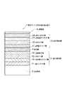
以下、図面を参照して本発明の第1実施形態を説明する。図1は、本発明の半導体素子の製造方法によって製造された窒化ガリウム系半導体発光素子の断面構造を示す。 Hereinafter, a first embodiment of the present invention will be described with reference to the drawings. FIG. 1 shows a cross-sectional structure of a gallium nitride based semiconductor light emitting device manufactured by the method for manufacturing a semiconductor device of the present invention.
図1に示すように、窒化ガリウム系半導体発光素子1は、n型のGaN基板2上に、n型半導体層3、活性層4、p型半導体層5が順次積層されている。また、p型半導体層5の上面には、金属製のp側電極6が形成されると共に、n型半導体層3には、後述するn型コンタクト層11にn側電極(図示略)が形成されている。
As shown in FIG. 1, the gallium nitride based semiconductor light-
n型半導体層3は、GaN基板2側から順に、n型GaN層からなるn型コンタクト層11、約25Åの厚みのn型Al0.16Ga0.84N層及び約25Åの厚みのn型GaN層が各260層積層された約13000Åの厚みのn型超格子クラッド層12、約700Åの厚みのn型GaN層からなるn型ガイド層13、n型InGaN層とn型GaN層が交互に複数積層されたn型超格子層14が順次積層されている。
The n-
活性層4は、Inの組成比の異なる2つのInGaN層からなる障壁層及び井戸層が交互に複数積層されている。
In the
p型半導体層5は、活性層4側から順に、約200Åの厚みのAl0.2Ga0.8N層からなるp型電子バリア層21、約1000Åの厚みのp型ガイド層22、約25Åの厚みのp型Al0.16Ga0.84N層及び約25Åの厚みのp型GaN層が各80層積層された約4000Åの厚みのp型超格子クラッド層23、約500Åの厚みのp型GaN層からなるp型コンタクト層24が順次積層されている。
The p-
この窒化ガリウム系光半導体発光素子1では、n側電極及びp側電極6からキャリアが供給されると、n型半導体層3及びp型半導体層5を介して、活性層4に注入される。そして、活性層4に注入されたキャリアが結合することによって、光を発光する。
In this gallium nitride based optical semiconductor
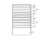
次に、上述した窒化ガリウム系半導体発光素子の製造方法について、図2〜図5を参照して説明する。図2〜図5は、実施形態に係る窒化ガリウム系半導体発光素子の各製造工程の断面構造を示す図である。 Next, a method for manufacturing the above-described gallium nitride based semiconductor light emitting device will be described with reference to FIGS. 2-5 is a figure which shows the cross-sectional structure of each manufacturing process of the gallium nitride based semiconductor light-emitting device according to the embodiment.
まず、図2に示すように、MOCVD法等の既知の方法によって、n型のGaN基板2を約1050℃の成長温度に保持した状態で、GaN基板2上に、n型コンタクト層11、n型超格子クラッド層12、n型ガイド層13を順次成長させる。次に、GaN基板2を約780℃の成長温度に下げてn型超格子層14、活性層4を順次成長させた後、GaN基板2を約1070℃の成長温度まで上げてp型電子バリア層21を成長させる。次に、GaN基板2を約1000℃の成長温度まで下げてp型ガイド層22を成長させた後、GaN基板2を約1050℃の成長温度まで上げてp型超格子クラッド層23を成長させる。次に、GaN基板2を約1000℃の温度に下げた状態で、約500Åの厚みのp型GaN層からなるp型コンタクト層24を成長させる。
First, as shown in FIG. 2, the n-
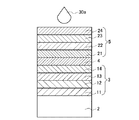
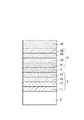
次に、p型コンタクト層24上にSiO2からなる約1000Åの厚みの絶縁膜30を塗布及びベーキングすることによって成膜する。具体的には、図3に示すように、ジブチルエーテル溶液にポリシラザンを溶解させた絶縁膜材30aをp型コンタクト層24上に滴下する。次に、図4に示すように、スピンコート法によって絶縁膜材30aをp型コンタクト層24の上面に渡って延ばして塗布したものを加水分解又は重縮合反応させた後、多段階ベーキングを行うことによってSiO2からなる絶縁膜30を成膜する。多段階ベーキングは、成膜する絶縁膜30によって異なるが、例えば、約220℃で2分間行った後、約350℃で約2分間行い、最後に、約400℃で30分間行う多段階ベーキングを適用することができる。尚、絶縁膜30の厚みを1000Å以上にする場合には、上述した絶縁膜の形成工程を複数回行ってもよいが、半導体層のクラックを防ぐためには、絶縁膜30の厚みは10000Å以下にすることが望ましい。このように、絶縁膜30を10000Å以下にすることによって、p型コンタクト層24と絶縁膜30との熱膨張率の違いに起因する、p型コンタクト層24のクラック等の破損を防止することができる。
Next, an
次に、約900℃以上の温度の窒素又は窒素と酸素を含む大気圧の雰囲気中でアニールすることによって、p型コンタクト層24を含むp型半導体層5内のアクセプタ(Mg)を活性化して、p型半導体層5をp型化する。
Next, the acceptor (Mg) in the p-
次に、図5に示すように、約14.9%の濃度を有する約25℃のBHF(一水素二フッ化アンモニウム)溶液でウェットエッチングすることにより、p型コンタクト層24上から絶縁膜30を除去する。このように絶縁膜30を成膜した後ウェットエッチングによって除去することによって、p型コンタクト層24のp側電極6が形成される面上の多くの自然酸化膜や汚染物を絶縁膜30と共に除去することができる。
Next, as shown in FIG. 5, the
最後に、次に、p側電極6を既知の方法によって形成した後、電子線照射やアニールによってオーミックコンタクトを形成する。最後にn側電極を形成して、窒化ガリウム系半導体発光素子1が完成する。
Finally, after forming the p-side electrode 6 by a known method, an ohmic contact is formed by electron beam irradiation or annealing. Finally, an n-side electrode is formed to complete the gallium nitride based semiconductor
上述したように本発明による窒化ガリウム系半導体発光素子の製造方法では、p型コンタクト層24上に絶縁膜30を形成した状態でp型半導体層21〜24のアクセプタを活性化しているので、約900℃以上でアニールを行っても、p型コンタクト層24から窒素が放出されることを抑制することができる。これによって、p型コンタクト層24のMgの活性化を高めて抵抗値を低減することができる。
As described above, in the method for manufacturing a gallium nitride based semiconductor light emitting device according to the present invention, the acceptors of the p-type semiconductor layers 21 to 24 are activated with the insulating
また、このように絶縁膜材30aを塗布することによってp型コンタクト層24上に絶縁膜30を形成することにより、プラズマCVD法によって絶縁膜をp型コンタクト層に形成した場合に受けるp型コンタクト層上のダメージを防ぐことができる。これによって、p型コンタクト層24上のダメージに起因するp型コンタクト層24とp側電極6との間の抵抗値の増大を防ぐことができるので、p型コンタクト層24とp側電極6との間に良好なオーミックコンタクトを形成することができる。
Further, by forming the insulating
また、絶縁膜30をp型コンタクト層24上に形成することにより、p型コンタクト層24から窒素が放出されることを抑制することができるので、大気圧の窒素を含む雰囲気中でアニールすることができる。この結果、アニールの工程を簡単化することができる。
Further, since the insulating
次に、図面を参照して、p型コンタクト層上に絶縁膜を形成した後アニールすることによって、p型コンタクト層とp側電極との間の抵抗値が低減する効果を証明するために行った実験について説明する。 Next, referring to the drawings, an insulating film is formed on the p-type contact layer and then annealed to prove the effect of reducing the resistance value between the p-type contact layer and the p-side electrode. The experiment will be described.
まず、上述の実験を行うために作製した本発明及び比較例による試料について説明する。図6は、実験のために作製した試料の断面構造を示す図である。 First, a sample according to the present invention and a comparative example prepared for conducting the above-described experiment will be described. FIG. 6 is a diagram showing a cross-sectional structure of a sample manufactured for the experiment.
図6に示すように、試料41は、n型GaN層42と、n型GaN層42上に形成されたp型GaN層43を備えている。p型GaN層43には、Pd及びAuからなるp側電極44が形成されると共に、n型GaN層42には、Ti及びAlからなるn側電極45が形成されている。 As shown in FIG. 6, the sample 41 includes an n-type GaN layer 42 and a p-type GaN layer 43 formed on the n-type GaN layer 42. A p-side electrode 44 made of Pd and Au is formed on the p-type GaN layer 43, and an n-side electrode 45 made of Ti and Al is formed on the n-type GaN layer 42.
この試料41は、n型GaN層42上にp型GaN層43及びPd/Auからなるp側電極44を順次積層した後、p側電極44、p型GaN層43及びn型GaN層42の一部をメサエッチングし、露出したn型GaN層42の一部にTi/Alからなるn側電極45を形成することによって、作製した。 In this sample 41, a p-type GaN layer 43 and a p-side electrode 44 made of Pd / Au are sequentially stacked on an n-type GaN layer 42, and then the p-side electrode 44, the p-type GaN layer 43, and the n-type GaN layer 42 are formed. A part of the n-type GaN layer 42 was formed by mesa etching, and an n-side electrode 45 made of Ti / Al was formed.
ここで、本発明による試料41は、p型GaN層43を形成した後、p側電極44を形成する前に、上述の実施形態で説明した製造方法に基づいて、約1000Åの絶縁膜を形成した後、約910℃で約10分間、大気圧の窒素雰囲気中でアニールを行い、その後、BHF溶液で絶縁膜を除去した。一方、比較用の試料41は、p型GaN層43を形成した後、絶縁膜を形成することなく、約800℃で約10分間、大気圧の窒素雰囲気中でアニールを行った。 Here, in the sample 41 according to the present invention, after the p-type GaN layer 43 is formed and before the p-side electrode 44 is formed, an insulating film of about 1000 mm is formed based on the manufacturing method described in the above embodiment. After that, annealing was performed at about 910 ° C. for about 10 minutes in a nitrogen atmosphere at atmospheric pressure, and then the insulating film was removed with a BHF solution. On the other hand, after the p-type GaN layer 43 was formed, the comparative sample 41 was annealed in a nitrogen atmosphere at atmospheric pressure at about 800 ° C. for about 10 minutes without forming an insulating film.
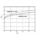
まず、図7を参照して電流−電圧特性を調べた実験結果について説明する。図7は、試料に流した電流と電圧との関係を示す図である。尚、横軸が流した電流を示し、縦軸がその際の電圧を示す。この実験は、p側電極44とn側電極45との間に流す電流の電流値を徐々に上げ、各電流値での電圧値を測定した。 First, the experimental results of examining the current-voltage characteristics will be described with reference to FIG. FIG. 7 is a diagram showing the relationship between the current and voltage applied to the sample. The horizontal axis indicates the current that flows and the vertical axis indicates the voltage at that time. In this experiment, the current value of the current passed between the p-side electrode 44 and the n-side electrode 45 was gradually increased, and the voltage value at each current value was measured.
図7に示すように、p型GaN層43に絶縁膜を形成した状態でアニールを行った本発明による試料41は、p型GaN層43に絶縁膜を形成せずにアニールを行った比較例の試料41に比べて抵抗値が高いことがわかる。これは、本発明による試料41は、p型GaN層43上に絶縁膜を形成した状態でアニールを行うことによって、比較例の試料41に比べて、p型GaN層43から抜ける窒素を抑制することができたためと考えられる。 As shown in FIG. 7, the sample 41 according to the present invention annealed with the insulating film formed on the p-type GaN layer 43 is a comparative example in which the p-type GaN layer 43 was annealed without forming the insulating film. It can be seen that the resistance value is higher than that of the sample 41. This is because the sample 41 according to the present invention suppresses nitrogen released from the p-type GaN layer 43 as compared with the sample 41 of the comparative example by performing annealing in a state where an insulating film is formed on the p-type GaN layer 43. It is thought that it was possible.
次に、p型コンタクト層の抵抗率及びホール濃度の向上を証明するために行った実験について説明する。この抵抗率及びホール濃度の測定は、矩形状のp型GaN層を形成し、そのp型GaN層の四隅に電極を設けてvan der Pauw法によって行った。 Next, an experiment conducted to prove an improvement in resistivity and hole concentration of the p-type contact layer will be described. The resistivity and the hole concentration were measured by a van der Pauw method by forming a rectangular p-type GaN layer and providing electrodes at the four corners of the p-type GaN layer.
まず、抵抗率を測定した実験結果について説明する。本発明による試料として、上述の製造方法により絶縁膜を形成した状態で、約910℃で約10分間アニールしたp型GaN層を作製した。そして、比較用の試料として、絶縁膜を形成せずに、約800℃で約10分間アニールしたp型GaN層を作製した。上述したp型GaN層による試料の抵抗率は約1.74Ω・cmとなったのに対し、比較例によるp型GaN層の抵抗率は、本発明の試料の約1.3倍に当たる約2.31Ω・cmとなった。このことからも、本発明によるp型GaN層の抵抗値が低減していることがわかる。 First, the experimental results of measuring the resistivity will be described. As a sample according to the present invention, a p-type GaN layer annealed at about 910 ° C. for about 10 minutes with the insulating film formed by the above-described manufacturing method was produced. Then, as a comparative sample, a p-type GaN layer annealed at about 800 ° C. for about 10 minutes without forming an insulating film was produced. The resistivity of the sample by the p-type GaN layer is about 1.74 Ω · cm, whereas the resistivity of the p-type GaN layer according to the comparative example is about 2 times, which is about 1.3 times that of the sample of the present invention. It was 31 Ω · cm. This also shows that the resistance value of the p-type GaN layer according to the present invention is reduced.
次に、ホール濃度を測定した実験結果について説明する。本発明による試料として、上述の製造方法により絶縁膜を形成した状態で、約900℃で約10分間アニールしたp型GaN層と、約925℃で約10分間アニールしたp型GaN層を作製した。そして、比較用の試料として、絶縁膜を形成せずに、約800℃で約10分間アニールしたp型GaN層を作製した。本発明によるp型GaN層のホール濃度は、約900℃でアニールしたものが約8.27×1017cm−3となり、約925℃でアニールしたものが約8.91×1017cm−3となった。一方、約800℃でアニールした比較用のp型GaN層のホール濃度は、約7.41×1017cm−3となった。従って、本発明による製造方法によって作製されたp型GaN層は、比較用のp型GaN層に比べてホール濃度が向上していることがわかる。このことからも、本発明の製造方法は、p型GaN層の抵抗値を低減できることがわかる。 Next, the experimental results of measuring the hole concentration will be described. As a sample according to the present invention, a p-type GaN layer annealed at about 900 ° C. for about 10 minutes and a p-type GaN layer annealed at about 925 ° C. for about 10 minutes with an insulating film formed by the above-described manufacturing method were produced. . Then, as a comparative sample, a p-type GaN layer annealed at about 800 ° C. for about 10 minutes without forming an insulating film was produced. The hole concentration of the p-type GaN layer according to the present invention is about 8.27 × 10 17 cm −3 when annealed at about 900 ° C., and about 8.91 × 10 17 cm −3 when annealed at about 925 ° C. It became. On the other hand, the hole concentration of the comparative p-type GaN layer annealed at about 800 ° C. was about 7.41 × 10 17 cm −3 . Therefore, it can be seen that the hole concentration of the p-type GaN layer produced by the manufacturing method according to the present invention is higher than that of the comparative p-type GaN layer. This also shows that the manufacturing method of the present invention can reduce the resistance value of the p-type GaN layer.
以上、上記実施形態を用いて本発明を詳細に説明したが、本発明が本明細書中に説明した実施形態に限定されるものではないということは明らかである。本発明は、特許請求の範囲の記載により定まる本発明の趣旨及び範囲内で変更して実施することができる。即ち、本明細書の記載は、一例であり、本発明を何ら限定的な意味に解釈させるものではない。以下、上記実施形態を一部変更した変更形態について説明する。 As mentioned above, although this invention was demonstrated in detail using the said embodiment, it is clear that this invention is not limited to embodiment described in this specification. The present invention can be implemented with modifications within the spirit and scope of the present invention defined by the description of the scope of claims. That is, the description of the present specification is an example, and the present invention is not construed as being limited in any way. Hereinafter, modified embodiments in which the above-described embodiment is partially modified will be described.
例えば、上述の実施形態では、SiO2からなる絶縁膜30を用いたが、他の酸化物又はSiN等の窒化物からなる絶縁膜を適用してもよい。
For example, in the above-described embodiment, the insulating
また、上述の実施形態では、絶縁膜30を除去する酸として、BHF溶液を用いたが、BHF溶液の代わりにフッ酸系溶液等の他の酸を用いることもできる。
In the above-described embodiment, the BHF solution is used as the acid for removing the insulating
また、上述の実施形態では、絶縁膜材30aを滴下した後、塗布したが、スプレー等によって絶縁膜材30aをp型コンタクト層24上に塗布してもよい。また、絶縁膜材を塗布した後、ベーキングではなく、電子線や紫外線を照射することによって絶縁膜を形成してもよい。
In the above-described embodiment, the insulating
また、上述の実施形態では、p型コンタクト層24をp型GaN層によって構成したが、p型InGaN層等、他のp型GaN系半導体層によって構成してもよい。
In the above-described embodiment, the p-
1 窒化ガリウム系半導体発光素子
2 GaN基板
3 n型半導体層
4 活性層
5 p型半導体層
6 p側電極
11 n型コンタクト層
12 n型超格子クラッド層
13 n型ガイド層
14 n型超格子層
21 p型電子バリア層
22 p型ガイド層
23 p型超格子クラッド層
24 p型コンタクト層
30 絶縁膜
30a 絶縁膜材
DESCRIPTION OF
Claims (3)
前記p型コンタクト層の前記p側電極が形成される面に絶縁膜材を塗布することによって絶縁膜を成膜する工程と、
前記p型半導体層をアニールする工程とを備えたことを特徴とする半導体素子の製造方法。 growing a p-type semiconductor layer including a p-type contact layer made of a p-type GaN-based semiconductor layer and forming a p-side electrode;
Forming an insulating film by applying an insulating film material to a surface of the p-type contact layer on which the p-side electrode is formed;
And a step of annealing the p-type semiconductor layer.
The method for manufacturing a semiconductor device according to claim 1, wherein the annealing is performed in an atmosphere containing nitrogen at atmospheric pressure.
Priority Applications (2)
| Application Number | Priority Date | Filing Date | Title |
|---|---|---|---|
| JP2006079521A JP2007258376A (en) | 2006-03-22 | 2006-03-22 | Manufacturing method of semiconductor element |
| US11/723,959 US20070232084A1 (en) | 2006-03-22 | 2007-03-22 | Manufacturing method for semiconductor device |
Applications Claiming Priority (1)
| Application Number | Priority Date | Filing Date | Title |
|---|---|---|---|
| JP2006079521A JP2007258376A (en) | 2006-03-22 | 2006-03-22 | Manufacturing method of semiconductor element |
Publications (1)
| Publication Number | Publication Date |
|---|---|
| JP2007258376A true JP2007258376A (en) | 2007-10-04 |
Family
ID=38559742
Family Applications (1)
| Application Number | Title | Priority Date | Filing Date |
|---|---|---|---|
| JP2006079521A Pending JP2007258376A (en) | 2006-03-22 | 2006-03-22 | Manufacturing method of semiconductor element |
Country Status (2)
| Country | Link |
|---|---|
| US (1) | US20070232084A1 (en) |
| JP (1) | JP2007258376A (en) |
Citations (4)
| Publication number | Priority date | Publication date | Assignee | Title |
|---|---|---|---|---|
| JP2540791B2 (en) * | 1991-11-08 | 1996-10-09 | 日亜化学工業株式会社 | A method for manufacturing a p-type gallium nitride-based compound semiconductor. |
| JPH11243209A (en) * | 1998-02-25 | 1999-09-07 | Seiko Epson Corp | Transfer method of thin-film device, the thin-film device, thin-film integrated circuit device, active matrix substrate, liquid crystal display device, and electronic apparatus |
| JP2002314131A (en) * | 2001-04-10 | 2002-10-25 | Showa Denko Kk | Transparent electrode, manufacturing method thereof and group iii nitride semiconductor light emitting element using the same |
| JP2005019972A (en) * | 2003-05-30 | 2005-01-20 | Showa Denko Kk | Method of manufacturing group iii nitride semiconductor device |
Family Cites Families (1)
| Publication number | Priority date | Publication date | Assignee | Title |
|---|---|---|---|---|
| JP4060511B2 (en) * | 2000-03-28 | 2008-03-12 | パイオニア株式会社 | Method for separating nitride semiconductor device |
-
2006
- 2006-03-22 JP JP2006079521A patent/JP2007258376A/en active Pending
-
2007
- 2007-03-22 US US11/723,959 patent/US20070232084A1/en not_active Abandoned
Patent Citations (4)
| Publication number | Priority date | Publication date | Assignee | Title |
|---|---|---|---|---|
| JP2540791B2 (en) * | 1991-11-08 | 1996-10-09 | 日亜化学工業株式会社 | A method for manufacturing a p-type gallium nitride-based compound semiconductor. |
| JPH11243209A (en) * | 1998-02-25 | 1999-09-07 | Seiko Epson Corp | Transfer method of thin-film device, the thin-film device, thin-film integrated circuit device, active matrix substrate, liquid crystal display device, and electronic apparatus |
| JP2002314131A (en) * | 2001-04-10 | 2002-10-25 | Showa Denko Kk | Transparent electrode, manufacturing method thereof and group iii nitride semiconductor light emitting element using the same |
| JP2005019972A (en) * | 2003-05-30 | 2005-01-20 | Showa Denko Kk | Method of manufacturing group iii nitride semiconductor device |
Also Published As
| Publication number | Publication date |
|---|---|
| US20070232084A1 (en) | 2007-10-04 |
Similar Documents
| Publication | Publication Date | Title |
|---|---|---|
| JP4599442B2 (en) | Manufacturing method of semiconductor light emitting device | |
| JP5060656B2 (en) | Nitride semiconductor light emitting device and manufacturing method thereof | |
| JP3723434B2 (en) | Semiconductor light emitting device | |
| EP2472605A1 (en) | Nitride semiconductor element and process for production thereof | |
| US7964424B2 (en) | Method for manufacturing nitride semiconductor light-emitting element | |
| JP2010045098A (en) | Method of manufacturing group-iii nitride semiconductor layer bonded substrate | |
| JP2007184353A (en) | Nitride-based compound semiconductor element and manufacturing method thereof | |
| JP2018125430A (en) | Semiconductor light-emitting element and method for manufacturing the same | |
| US20050159000A1 (en) | Method for fabricating nitride-based compound semiconductor element | |
| TWI381557B (en) | Light emitting diode device and method for fabricating thereof | |
| JPWO2020121794A1 (en) | Nitride-based semiconductor light-emitting device and its manufacturing method, and method for manufacturing nitride-based semiconductor crystal | |
| JP5749888B2 (en) | Semiconductor device and method for manufacturing the semiconductor device | |
| JP5067158B2 (en) | Electrode structure, semiconductor element, and manufacturing method thereof | |
| JP5977513B2 (en) | Manufacturing method of nitride semiconductor device | |
| JP5083973B2 (en) | Method for manufacturing optical semiconductor element | |
| JP6002109B2 (en) | Method for manufacturing group III nitride semiconductor device | |
| JPH11177135A (en) | Gallium nitride semiconductor element and its manufacture | |
| JP4136746B2 (en) | Method of forming nitride semiconductor and nitride semiconductor device | |
| JP2007258376A (en) | Manufacturing method of semiconductor element | |
| JP5607106B2 (en) | Nitride semiconductor light emitting device and manufacturing method thereof | |
| JP5136615B2 (en) | Method for manufacturing group III nitride semiconductor light emitting device | |
| JP2007258375A (en) | Manufacturing method of semiconductor element | |
| JP2007258248A (en) | MANUFACTURING METHOD OF GaN-BASED SEMICONDUCTOR ELEMENT, AND GaN-BASED SEMICONDUCTOR ELEMENT | |
| US11658261B2 (en) | Method of manufacturing nitride semiconductor device | |
| JP2012004457A (en) | Manufacturing method of semiconductor light-emitting element |
Legal Events
| Date | Code | Title | Description |
|---|---|---|---|
| A621 | Written request for application examination |
Free format text: JAPANESE INTERMEDIATE CODE: A621 Effective date: 20090206 |
|
| A131 | Notification of reasons for refusal |
Free format text: JAPANESE INTERMEDIATE CODE: A131 Effective date: 20110531 |
|
| A977 | Report on retrieval |
Free format text: JAPANESE INTERMEDIATE CODE: A971007 Effective date: 20110601 |
|
| A02 | Decision of refusal |
Free format text: JAPANESE INTERMEDIATE CODE: A02 Effective date: 20111018 |