JP2007250060A - Semiconductor storage device - Google Patents
Semiconductor storage device Download PDFInfo
- Publication number
- JP2007250060A JP2007250060A JP2006070587A JP2006070587A JP2007250060A JP 2007250060 A JP2007250060 A JP 2007250060A JP 2006070587 A JP2006070587 A JP 2006070587A JP 2006070587 A JP2006070587 A JP 2006070587A JP 2007250060 A JP2007250060 A JP 2007250060A
- Authority
- JP
- Japan
- Prior art keywords
- memory cell
- bit line
- sub
- cell array
- cell arrays
- Prior art date
- Legal status (The legal status is an assumption and is not a legal conclusion. Google has not performed a legal analysis and makes no representation as to the accuracy of the status listed.)
- Pending
Links
- 239000004065 semiconductor Substances 0.000 title claims abstract description 20
- 238000003491 array Methods 0.000 claims abstract description 38
- 230000003213 activating effect Effects 0.000 claims description 6
- 230000004044 response Effects 0.000 claims description 3
- 238000007689 inspection Methods 0.000 abstract description 22
- 230000000295 complement effect Effects 0.000 description 9
- 238000010586 diagram Methods 0.000 description 4
- 238000000034 method Methods 0.000 description 4
- 102100039788 GTPase NRas Human genes 0.000 description 2
- 101000744505 Homo sapiens GTPase NRas Proteins 0.000 description 2
- 230000003321 amplification Effects 0.000 description 2
- 238000003199 nucleic acid amplification method Methods 0.000 description 2
- 239000003990 capacitor Substances 0.000 description 1
- 230000002950 deficient Effects 0.000 description 1
- 230000014759 maintenance of location Effects 0.000 description 1
- 238000004904 shortening Methods 0.000 description 1
Images

Classifications
-
- G—PHYSICS
- G11—INFORMATION STORAGE
- G11C—STATIC STORES
- G11C11/00—Digital stores characterised by the use of particular electric or magnetic storage elements; Storage elements therefor
- G11C11/21—Digital stores characterised by the use of particular electric or magnetic storage elements; Storage elements therefor using electric elements
- G11C11/34—Digital stores characterised by the use of particular electric or magnetic storage elements; Storage elements therefor using electric elements using semiconductor devices
- G11C11/40—Digital stores characterised by the use of particular electric or magnetic storage elements; Storage elements therefor using electric elements using semiconductor devices using transistors
- G11C11/401—Digital stores characterised by the use of particular electric or magnetic storage elements; Storage elements therefor using electric elements using semiconductor devices using transistors forming cells needing refreshing or charge regeneration, i.e. dynamic cells
- G11C11/4063—Auxiliary circuits, e.g. for addressing, decoding, driving, writing, sensing or timing
- G11C11/407—Auxiliary circuits, e.g. for addressing, decoding, driving, writing, sensing or timing for memory cells of the field-effect type
- G11C11/409—Read-write [R-W] circuits
- G11C11/4097—Bit-line organisation, e.g. bit-line layout, folded bit lines
-
- G—PHYSICS
- G11—INFORMATION STORAGE
- G11C—STATIC STORES
- G11C29/00—Checking stores for correct operation ; Subsequent repair; Testing stores during standby or offline operation
- G11C29/04—Detection or location of defective memory elements, e.g. cell constructio details, timing of test signals
- G11C29/50—Marginal testing, e.g. race, voltage or current testing
- G11C29/50016—Marginal testing, e.g. race, voltage or current testing of retention
-
- G—PHYSICS
- G11—INFORMATION STORAGE
- G11C—STATIC STORES
- G11C7/00—Arrangements for writing information into, or reading information out from, a digital store
- G11C7/18—Bit line organisation; Bit line lay-out
-
- G—PHYSICS
- G11—INFORMATION STORAGE
- G11C—STATIC STORES
- G11C11/00—Digital stores characterised by the use of particular electric or magnetic storage elements; Storage elements therefor
- G11C11/21—Digital stores characterised by the use of particular electric or magnetic storage elements; Storage elements therefor using electric elements
- G11C11/34—Digital stores characterised by the use of particular electric or magnetic storage elements; Storage elements therefor using electric elements using semiconductor devices
- G11C11/40—Digital stores characterised by the use of particular electric or magnetic storage elements; Storage elements therefor using electric elements using semiconductor devices using transistors
- G11C11/401—Digital stores characterised by the use of particular electric or magnetic storage elements; Storage elements therefor using electric elements using semiconductor devices using transistors forming cells needing refreshing or charge regeneration, i.e. dynamic cells
-
- G—PHYSICS
- G11—INFORMATION STORAGE
- G11C—STATIC STORES
- G11C29/00—Checking stores for correct operation ; Subsequent repair; Testing stores during standby or offline operation
- G11C29/04—Detection or location of defective memory elements, e.g. cell constructio details, timing of test signals
- G11C29/08—Functional testing, e.g. testing during refresh, power-on self testing [POST] or distributed testing
- G11C29/12—Built-in arrangements for testing, e.g. built-in self testing [BIST] or interconnection details
- G11C2029/1204—Bit line control
-
- G—PHYSICS
- G11—INFORMATION STORAGE
- G11C—STATIC STORES
- G11C29/00—Checking stores for correct operation ; Subsequent repair; Testing stores during standby or offline operation
- G11C29/04—Detection or location of defective memory elements, e.g. cell constructio details, timing of test signals
- G11C29/08—Functional testing, e.g. testing during refresh, power-on self testing [POST] or distributed testing
- G11C29/12—Built-in arrangements for testing, e.g. built-in self testing [BIST] or interconnection details
- G11C29/18—Address generation devices; Devices for accessing memories, e.g. details of addressing circuits
- G11C29/26—Accessing multiple arrays
- G11C2029/2602—Concurrent test
-
- G—PHYSICS
- G11—INFORMATION STORAGE
- G11C—STATIC STORES
- G11C2207/00—Indexing scheme relating to arrangements for writing information into, or reading information out from, a digital store
- G11C2207/002—Isolation gates, i.e. gates coupling bit lines to the sense amplifier
Abstract
Description
本発明は、半導体記憶装置に関し、より特定的には、ダイナミックランダムアクセスメモリ(DRAM)において、メモリセルトランジスタのリーク不良を検出するためのテスト回路を備えた半導体記憶装置に関する。 The present invention relates to a semiconductor memory device, and more particularly, to a semiconductor memory device including a test circuit for detecting a leak failure of a memory cell transistor in a dynamic random access memory (DRAM).
従来の半導体記憶装置、特にDRAMにおけるメモリセルトランジスタのリーク不良を検出する検査(以下、ディスターブリフレッシュ検査という)として、例えば次の手法が存在する。 As a test for detecting a leak failure of a memory cell transistor in a conventional semiconductor memory device, particularly a DRAM (hereinafter referred to as a disturb refresh test), for example, the following method exists.
まず、全メモリセルにHigh(又はLow)データを書き込む。全メモリセルへの書き込み動作(ライト動作)の後、ある任意のワード線を活性化させて直交するビット線にメモリセルの電荷を読み出す。そして、その読み出した電荷をセンスアンプ回路において増幅(リード/リフレッシュ動作)することで、ビット線及び相補ビット線の電位をHigh又はLowにする。この状態は、メモリセルのデータ保持時間を保証可能な時間(以下、リフレッシュ検査時間という)だけ保持される。 First, high (or low) data is written in all memory cells. After a write operation (write operation) to all memory cells, a certain arbitrary word line is activated to read out memory cell charges to orthogonal bit lines. Then, the read charges are amplified (read / refresh operation) in the sense amplifier circuit, so that the potentials of the bit line and the complementary bit line are set to High or Low. This state is maintained only for a time during which the data retention time of the memory cell can be guaranteed (hereinafter referred to as refresh inspection time).
この状態において、非選択ワードに接続されているメモリセルキャパシタは、Highデータが保持されており、かつ接続されているビット線がLowレベルになっているメモリセルに対しては、メモリセルトランジスタのドレイン−ソース間に電位差が生じ、サブスレショルド電流が流れる。ここで、トランジスタのしきい値電圧が低いメモリセルの場合、サブスレショルド電流が多く流れるため、リフレッシュ検査時間内でデータ保持ができず不良セルとなる。よって、リフレッシュ検査時間終了後に、検査対象メモリセルに対して読み出し動作を行い、データが正しく読み出されるかどうかを確認する。 In this state, the memory cell capacitor connected to the non-selected word holds the high data, and the memory cell transistor is connected to the memory cell in which the connected bit line is at the low level. A potential difference is generated between the drain and the source, and a subthreshold current flows. Here, in the case of a memory cell having a low threshold voltage of a transistor, a large amount of subthreshold current flows, so that data cannot be held within the refresh inspection time, resulting in a defective cell. Therefore, after the refresh inspection time ends, a read operation is performed on the memory cell to be inspected to check whether data is read correctly.
しかし、非選択ワードに接続されているメモリセルに対して、ビット線及び相補ビット線の電位をHigh又はLowにできるのは、メモリセル群とセンスアンプ回路とで構成されたメモリセルアレイ単位でしかできない。また、上記リフレッシュ検査時間は、通常数msから数十msのオーダーで設定されることが多く、この時間はメモリに対してデータの読み出し及び書き込みする時間に比べて十分に長いことから、ディスターブリフレッシュ検査は、メモリの検査時間の中で大きな割合を占めている。 However, the potential of the bit line and complementary bit line can be set to High or Low for the memory cells connected to the unselected word only in the memory cell array unit composed of the memory cell group and the sense amplifier circuit. Can not. In addition, the refresh inspection time is usually set on the order of several ms to several tens of ms, and this time is sufficiently longer than the time for reading and writing data to the memory. The inspection accounts for a large percentage of the memory inspection time.
このような課題に対して、テストモードに応じて複数のワード線を同時に活性化させる手法や複数メモリセルアレイを同時選択することで、上記ディスターブリフレッシュ検査の時間短縮を図る手法が用いられている(例えば、特許文献1を参照)。
近年のプロセス微細化及び高速化に伴い、メモリセルアレイ単位が縮小化され、その結果メモリセルアレイ数が増加している。また、小さいチップ面積で大きい記憶容量を実現することを目的として、いわゆる階層ビット線構造を有するメモリ、例えばDRAMが提案されている。このメモリでは、1つのメインビット線対に対応して複数のサブビット線対が設けられ、各サブビット線対は2つの選択トランジスタを介してメインビット線対に接続されている。 With recent process miniaturization and higher speed, the memory cell array unit has been reduced, and as a result, the number of memory cell arrays has increased. In order to realize a large storage capacity with a small chip area, a memory having a so-called hierarchical bit line structure, for example, a DRAM has been proposed. In this memory, a plurality of sub bit line pairs are provided corresponding to one main bit line pair, and each sub bit line pair is connected to the main bit line pair via two selection transistors.
しかし、上記階層ビット線構造を有するメモリの場合、階層ビット線単位をサブメモリセルアレイとすると、同一メモリセルアレイ内であっても非選択サブメモリセルアレイ内では、サブビット線はメインビット線から電気的に切り離される。このため、メモリセルトランジスタのソース−ドレイン間に十分な電位差を印加できない。そのため、サブメモリセルアレイ単位での検査が必要になり、検査時間の大幅な増加及び検査コストの上昇を招くという問題があった。 However, in the case of a memory having the above hierarchical bit line structure, if the hierarchical bit line unit is a sub memory cell array, the sub bit line is electrically connected to the main bit line in the non-selected sub memory cell array even in the same memory cell array. Disconnected. For this reason, a sufficient potential difference cannot be applied between the source and drain of the memory cell transistor. For this reason, inspection in units of sub-memory cell arrays is required, which causes a problem that inspection time is significantly increased and inspection costs are increased.
それ故に、本発明の目的は、階層ビット線構造においてメインビット線を含むメモリセルアレイ単位でディスターブリフレッシュ検査を行うことで、検査時間の短縮を実現させた半導体記憶装置を提供することである。 SUMMARY OF THE INVENTION Therefore, an object of the present invention is to provide a semiconductor memory device that realizes a reduction in inspection time by performing a disturb refresh inspection in a memory cell array unit including a main bit line in a hierarchical bit line structure.
本発明は、メモリセル群とセンスアンプ回路とから構成されるメモリセルアレイを複数備えた半導体記憶装置に向けられている。そして、上記目的を達成させるために、本発明の半導体記憶装置は、複数のメモリセルアレイが、複数のサブメモリセルアレイと、複数のサブメモリセルアレイのそれぞれに配置され、メモリセル群に接続されたサブビット線と、選択スイッチを介してサブビット線と接続され、かつセンスアンプ回路に接続される、メモリセルアレイ内に配置されたメインビット線と、外部入力されるテストモード信号に応じて、全てのメモリセルアレイに配置された全ての選択スイッチを活性化させる手段とを、それぞれ備える。 The present invention is directed to a semiconductor memory device including a plurality of memory cell arrays each including a memory cell group and a sense amplifier circuit. In order to achieve the above object, a semiconductor memory device according to the present invention includes a plurality of memory cell arrays arranged in each of a plurality of sub memory cell arrays and a plurality of sub memory cell arrays, and connected to a memory cell group. All memory cell arrays in accordance with a test bit signal externally input and a main bit line arranged in the memory cell array connected to a sub bit line through a selection switch and connected to a sense amplifier circuit. And a means for activating all the selection switches arranged in each.
又は、上記目的を達成させるために、本発明の半導体記憶装置は、複数のメモリセルアレイが、複数のサブメモリセルアレイと、複数のサブメモリセルアレイのそれぞれに配置され、メモリセル群に接続されたサブビット線と、選択スイッチを介してサブビット線と接続され、かつセンスアンプ回路に接続される、メモリセルアレイ内に配置されたメインビット線と、外部入力されるテストモード信号、アドレス信号、及び動作起動信号に応じて、選択されたメモリセルアレイに配置された選択スイッチのうち、選択ワード線を含む選択サブメモリセルアレイの選択スイッチを活性化させ、選択されなかったメモリセルアレイに配置された非選択サブメモリセルアレイ内の選択スイッチを非活性化させる手段と、選択されなかったメモリセルアレイに配置された非選択サブメモリセルアレイ内の選択スイッチを非活性化させた後に、再度活性化させる手段とを、それぞれ備える。 Alternatively, in order to achieve the above object, in the semiconductor memory device of the present invention, a plurality of memory cell arrays are arranged in each of the plurality of sub memory cell arrays and the plurality of sub memory cell arrays and connected to the memory cell group. A main bit line arranged in the memory cell array, connected to the sub bit line via the selection switch and connected to the sense amplifier circuit, and a test mode signal, an address signal, and an operation start signal inputted from the outside Accordingly, the selection switch of the selected sub memory cell array including the selected word line among the selection switches arranged in the selected memory cell array is activated, and the unselected sub memory cell array arranged in the unselected memory cell array Means for deactivating a select switch in the memory cell and a memory cell that has not been selected The selection switch in the non-selected sub-memory cell arrays arranged in a ray after deactivates, and means for re-activating, each comprising.
ここで、選択されたメモリセルアレイ内で、かつ非選択サブメモリセルアレイ内の選択スイッチが非活性状態になるタイミングは、選択ワード線が活性状態になる前であることが好ましい。
また、選択されたメモリセルアレイ内で、かつ非選択サブメモリセルアレイ内の選択スイッチが非活性状態から活性状態になるタイミングは、選択ワード線が活性状態になった後で、かつセンスアンプ回路が活性状態になった後であることが好ましい。
Here, the timing at which the selection switch in the selected memory cell array and in the non-selected sub memory cell array is deactivated is preferably before the selected word line is activated.
The timing at which the selection switch in the selected memory cell array and in the non-selected sub memory cell array is activated from the inactive state is activated after the selected word line is activated and the sense amplifier circuit is activated. It is preferable that the state is reached.
上記本発明によれば、階層ビット線構造においてメインビット線を含むメモリセルアレイ単位でのディスターブリフレッシュ検査が可能になり、検査時間の短縮が可能となる。また、本発明によれば、テストモード動作時にメインビット線に接続されるサブビット線の本数を減らしてビット線の負荷容量を減らすため、選択ワード線に接続されたメモリセルからの読み出し電位を増加させることができ、選択ワード線に接続されたメモリセルのデータを破壊することはない。 According to the present invention, the disturb refresh inspection can be performed for each memory cell array including the main bit line in the hierarchical bit line structure, and the inspection time can be shortened. According to the present invention, the read potential from the memory cell connected to the selected word line is increased in order to reduce the number of sub bit lines connected to the main bit line and reduce the load capacity of the bit line during the test mode operation. The data of the memory cell connected to the selected word line is not destroyed.
以下、本発明の実施の形態について、図面を参照しながら説明する。
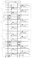
図1は、本発明の一実施形態に係る階層ビット線構造を持つメモリセル部を備える半導体記憶装置の概略構成を示す図である。図1において、本発明の半導体記憶装置は、サブビット線単位で構成される複数のサブメモリセルアレイ171〜174(この例では、4個のサブメモリセルアレイ)と、センスアンプ回路2とを含む。サブメモリセルアレイ171〜174は、電荷蓄積用の複数のメモリセルトランジスタと、サブビット線選択スイッチ141〜144とを、それぞれ備える。
Hereinafter, embodiments of the present invention will be described with reference to the drawings.
FIG. 1 is a diagram showing a schematic configuration of a semiconductor memory device including a memory cell unit having a hierarchical bit line structure according to an embodiment of the present invention. 1, the semiconductor memory device of the present invention includes a plurality of sub
センスアンプ回路2には、メインビット線20及び相補メインビット線21が接続される。メインビット線20及び相補メインビット線21は、サブビット線選択スイッチ141〜144を介して、サブビット線151〜154及び相補サブビット線161〜164に、それぞれ電気的に接続される。このサブビット線選択スイッチ141〜144は、サブビット線選択スイッチ制御信号181〜184によって制御される。
A main bit line 20 and a complementary main bit line 21 are connected to the sense amplifier circuit 2. The main bit line 20 and the complementary main bit line 21 are electrically connected to the
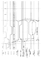
本発明の半導体記憶装置は、上記構成を用いて、次のような通常モード動作及びテストモード動作(2種類)を行う。図2は、通常モード動作時における各信号及びコマンドのタイミングチャートを示す図である。図3は、テストモード[1]動作時における各信号及びコマンドのタイミングチャートを示す図である。図4は、テストモード[2]動作時における各信号及びコマンドのタイミングチャートを示す図である。 The semiconductor memory device of the present invention performs the following normal mode operation and test mode operation (two types) using the above configuration. FIG. 2 is a diagram showing a timing chart of each signal and command during the normal mode operation. FIG. 3 is a diagram showing a timing chart of each signal and command during the test mode [1] operation. FIG. 4 is a timing chart of signals and commands during the test mode [2] operation.
まず、図2を参照して、テストモードが設定されていない通常モード動作を説明する。
通常モード動作のときは、テストモード信号はLowレベルに設定されている。メモリ動作がスタンバイ時、全てのサブビット線選択スイッチ141〜144が活性化状態になっていてプリチャージレベルがVDD/2レベルであるとすると、メインビット線20及びサブビット線151〜154も、VDD/2レベルになっている。
First, the normal mode operation in which the test mode is not set will be described with reference to FIG.
During the normal mode operation, the test mode signal is set to the low level. When the memory operation is in a standby state, if all the sub bit line selection switches 141 to 144 are activated and the precharge level is VDD / 2 level, the main bit line 20 and the
次のサイクルにて、外部入力コマンドのNRASとアドレス信号とによって、内部動作が開始される。この動作により、活性化メモリセルアレイ内においても、選択されたワード線を含むサブメモリセルアレイとその他のサブメモリセルアレイとで動作が異なる。ここで、ワード線121が選択された場合には、サブメモリセルアレイ171が選択されることになり、その他のサブメモリセルアレイ172〜174は、非選択サブメモリセルアレイとなる。そして、センスアンプ回路2内にあるビット線イコライズ回路(図示せず)は、非選択状態とほぼ同タイミングで、非選択サブメモリセルアレイ172〜174内のサブビット線選択スイッチ142〜144を非活性状態にさせる。
In the next cycle, the internal operation is started by the external input command NRAS and the address signal. With this operation, even in the activated memory cell array, the operation differs between the sub memory cell array including the selected word line and the other sub memory cell arrays. Here, when the word line 121 is selected, the sub
これにより、メインビット線20及び相補メインビット線21から非選択サブビット線152〜154及び非選択相補サブビット線162〜164を切り離すことができるため、ビット線の総負荷容量を減らすことが可能になる。そのため、メモリセルからの読み出し電位を多くすることができる。そして、選択ワード線を活性化することにより、メインビット線20に接続されたままの選択サブビット線151上にメモリセルからデータを読み出し、センスアンプ回路2で増幅する。この期間、非選択サブビット線152〜154は、電気的に切り離されているため高インピーダンス(Hi−Z)状態である。選択サブビット線151が十分に増幅された後にワード線121を非活性状態にし、その後、ビット線のイコライズ開始及び非選択サブメモリセルアレイ172〜174内のサブビット線選択スイッチ142〜144を活性状態へ戻す制御を行う。
As a result, the non-selected
次に、図3を参照して、第1のテストモードが設定されたテストモード[1]動作を説明する。
テストモード[1]動作と通常モード動作(図2)との違いは、テストモード信号がHighレベルに設定されている点と、非選択サブメモリセルアレイ172〜174内のサブビット線選択スイッチ142〜144が活性状態のままである点である。
Next, the test mode [1] operation in which the first test mode is set will be described with reference to FIG.
The difference between the test mode [1] operation and the normal mode operation (FIG. 2) is that the test mode signal is set to the high level and the sub bit line selection switches 142 to 144 in the unselected sub memory cell arrays 172 to 174. Is still active.
通常モード動作時では、内部動作が開始されると非選択サブメモリセルアレイ172〜174内のサブビット線選択スイッチ142〜144は非活性状態になるよう制御した。これに対し、テストモード[1]動作時では、非選択サブメモリセルアレイ172〜174内のサブビット線選択スイッチ142〜144は、活性化状態のままである。そのため、メインビット線20にサブビット線選択スイッチ141〜144を介して接続されている全てのサブビット線151〜154が接続された状態で、メモリセルからのデータ読み出し及びセンスアンプ回路2での増幅動作が行われる。
In the normal mode operation, the sub bit line selection switches 142 to 144 in the non-selected sub memory cell arrays 172 to 174 are controlled to be inactivated when the internal operation is started. On the other hand, in the test mode [1] operation, the sub bit line selection switches 142 to 144 in the non-selected sub memory cell arrays 172 to 174 remain in the activated state. Therefore, in the state where all the
よって、通常モード動作においては、非選択のサブメモリセルアレイのメモリセルトランジスタのソース−ドレイン間に十分な電位差が与えらず、メモリセルへのディスターブ検査ができないことが原因で、ディスターブ検査時間が増大するという課題があったが、本発明では、上述したテストモード[1]動作を用いて、非選択のサブビット線もHighレベル又はLowレベルに振幅するため、メモリセルアレイ単位での検査ができ、検査時間の短縮が可能になる。 Therefore, in the normal mode operation, the disturb inspection time is increased because a sufficient potential difference is not given between the source and drain of the memory cell transistor of the non-selected sub memory cell array, and the disturb inspection cannot be performed on the memory cell. However, in the present invention, since the non-selected sub-bit line also swings to the high level or the low level using the test mode [1] operation described above, the inspection can be performed in units of the memory cell array. Time can be shortened.
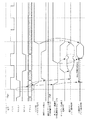
次に、図4を参照して、第2のテストモードが設定されたテストモード[2]動作を説明する。
外部入力コマンドのNRASとアドレス信号とによって、内部動作が開始される。これにより、通常モード動作と同じように、活性化メモリセルアレイ内においても選択されたワード線を含むサブメモリセルアレイとその他のサブメモリセルアレイとで異なる制御が行われる。ここで、外部入力アドレスによってワード線121が選択された場合には、サブメモリセルアレイ171が選択されることになり、その他のサブメモリセルアレイ172〜174は、非選択サブメモリセルアレイとなる。非選択サブメモリセルアレイ172〜174内のサブビット線選択スイッチ制御信号182〜184は、内部動作開始に応じて、サブビット線選択スイッチ142〜144を非選択状態にする。この選択サブビット線151のみをメインビット線20に接続する制御は、通常と同様である。
Next, the test mode [2] operation in which the second test mode is set will be described with reference to FIG.
The internal operation is started by the external input command NRAS and the address signal. As a result, as in the normal mode operation, different control is performed between the sub memory cell array including the selected word line and the other sub memory cell arrays in the activated memory cell array. Here, when the word line 121 is selected by the external input address, the sub
その後、選択サブビット線151にメモリセルからのデータ読み出し及びセンスアンプ回路2による増幅を行う。ここで、選択サブビット線151及びメインビット線20を十分に増幅した後、再度サブビット線選択スイッチ142〜144を活性化する。これにより、選択サブビット線151及びメインビット線20の振幅は、一時的にHigh側及びLow側共に下がるが、センスアンプ回路2が活性化状態でかつビット線も十分に振幅増幅した後なので、データを破壊することはない。
Thereafter, data reading from the memory cell and amplification by the sense amplifier circuit 2 are performed on the selected
これにより、テストモード[2]動作においても、テストモード[1]動作と同様に、非選択のサブビット線もHighレベル又はLowレベルに振幅するため、メモリセルアレイ単位での検査ができ、検査時間の短縮が可能になる。また、テストモード[1]動作では、選択サブビット線にメモリセルのデータを読み出した時に非選択サブビット線が接続されているため、ビット線の総負荷容量が通常モード動作時よりも多くなりデータの誤読み出しの可能性が非常に高いが、テストモード[2]動作では、データを読み出す時は通常モード動作と同じタイミングによってビット線の負荷容量が増加することを防ぎつつ、非選択ビット線へのディスターブリフレッシュ検査を可能とする。 As a result, in the test mode [2] operation, similarly to the test mode [1] operation, the non-selected sub-bit line also swings to the high level or the low level. Shortening becomes possible. In the test mode [1] operation, since the non-selected sub bit line is connected when the data of the memory cell is read to the selected sub bit line, the total load capacity of the bit line is larger than that in the normal mode operation, and the data is not stored. Although the possibility of erroneous reading is very high, in the test mode [2] operation, when data is read, the load capacity of the bit line is prevented from increasing at the same timing as in the normal mode operation, and the unselected bit line is read. Allows disturb refresh inspection.
以上のように本発明の一実施形態に係る階層ビット線構造を持つメモリセル部を備える半導体記憶装置によれば、階層ビット線構造においてメインビット線を含むメモリセルアレイ単位でのディスターブリフレッシュ検査が可能になり、検査時間の短縮が可能となる。また、本発明によれば、テストモード動作時にメインビット線に接続されるサブビット線の本数を減らしてビット線の負荷容量を減らすため、選択ワード線に接続されたメモリセルからの読み出し電位を増加させることができ、選択ワード線に接続されたメモリセルのデータを破壊することはない。 As described above, according to the semiconductor memory device including the memory cell unit having the hierarchical bit line structure according to the embodiment of the present invention, the disturb refresh test can be performed in the memory cell array unit including the main bit line in the hierarchical bit line structure. Thus, the inspection time can be shortened. According to the present invention, the read potential from the memory cell connected to the selected word line is increased in order to reduce the number of sub bit lines connected to the main bit line and reduce the load capacity of the bit line during the test mode operation. The data of the memory cell connected to the selected word line is not destroyed.
本発明は、DRAMを備えた半導体記憶装置等に利用可能であり、特にディスターブリフレッシュ検査時間を短縮させたい場合等に有用である。 The present invention can be used for a semiconductor memory device equipped with a DRAM, and is particularly useful when it is desired to shorten the disturb refresh inspection time.
20 メインビット線
21 相補メインビット線
121〜136 ワード線
141〜144 サブビット線選択スイッチ
151〜154 サブビット線
161〜164 相補サブビット線
171〜174 サブメモリセルアレイ
181〜184 サブビット線選択スイッチ制御信号
20 Main bit line 21 Complementary main bit lines 121 to 136
Claims (4)
前記複数のメモリセルアレイは、それぞれ
複数のサブメモリセルアレイと、
前記複数のサブメモリセルアレイのそれぞれに配置され、前記メモリセル群に接続されたサブビット線と、
選択スイッチを介して前記サブビット線と接続され、かつ前記センスアンプ回路に接続される、前記メモリセルアレイ内に配置されたメインビット線と、
外部入力されるテストモード信号に応じて、全ての前記メモリセルアレイに配置された全ての前記選択スイッチを活性化させる手段とを備える、半導体記憶装置。 A semiconductor memory device including a plurality of memory cell arrays each including a memory cell group and a sense amplifier circuit,
Each of the plurality of memory cell arrays includes a plurality of sub memory cell arrays,
A sub bit line disposed in each of the plurality of sub memory cell arrays and connected to the memory cell group;
A main bit line arranged in the memory cell array, connected to the sub-bit line via a selection switch and connected to the sense amplifier circuit;
And a means for activating all the selection switches arranged in all the memory cell arrays in response to an externally input test mode signal.
前記複数のメモリセルアレイは、それぞれ
複数のサブメモリセルアレイと、
前記複数のサブメモリセルアレイのそれぞれに配置され、前記メモリセル群に接続されたサブビット線と、
選択スイッチを介して前記サブビット線と接続され、かつ前記センスアンプ回路に接続される、前記メモリセルアレイ内に配置されたメインビット線と、
外部入力されるテストモード信号、アドレス信号、及び動作起動信号に応じて、選択された前記メモリセルアレイに配置された前記選択スイッチのうち、選択ワード線を含む選択サブメモリセルアレイの選択スイッチを活性化させ、選択されなかった前記メモリセルアレイに配置された非選択サブメモリセルアレイ内の前記選択スイッチを非活性化させる手段と、
前記選択されなかったメモリセルアレイに配置された前記非選択サブメモリセルアレイ内の前記選択スイッチを非活性化させた後に、再度活性化させる手段とを備える、半導体記憶装置。 A semiconductor memory device including a plurality of memory cell arrays each including a memory cell group and a sense amplifier circuit,
Each of the plurality of memory cell arrays includes a plurality of sub memory cell arrays,
A sub bit line disposed in each of the plurality of sub memory cell arrays and connected to the memory cell group;
A main bit line arranged in the memory cell array, connected to the sub-bit line via a selection switch and connected to the sense amplifier circuit;
In response to an externally input test mode signal, address signal, and operation start signal, the selection switch of the selected sub memory cell array including the selected word line is activated among the selection switches arranged in the selected memory cell array. Means for deactivating the selection switch in the non-selected sub memory cell array arranged in the memory cell array that has not been selected,
And a means for activating the selection switch in the non-selected sub-memory cell array arranged in the non-selected memory cell array and then activating it again.
Priority Applications (2)
| Application Number | Priority Date | Filing Date | Title |
|---|---|---|---|
| JP2006070587A JP2007250060A (en) | 2006-03-15 | 2006-03-15 | Semiconductor storage device |
| US11/724,213 US7529144B2 (en) | 2006-03-15 | 2007-03-15 | Hierarchical semiconductor memory device capable of carrying out a disturb refresh test on a memory array basis |
Applications Claiming Priority (1)
| Application Number | Priority Date | Filing Date | Title |
|---|---|---|---|
| JP2006070587A JP2007250060A (en) | 2006-03-15 | 2006-03-15 | Semiconductor storage device |
Publications (2)
| Publication Number | Publication Date |
|---|---|
| JP2007250060A true JP2007250060A (en) | 2007-09-27 |
| JP2007250060A5 JP2007250060A5 (en) | 2009-03-19 |
Family
ID=38517657
Family Applications (1)
| Application Number | Title | Priority Date | Filing Date |
|---|---|---|---|
| JP2006070587A Pending JP2007250060A (en) | 2006-03-15 | 2006-03-15 | Semiconductor storage device |
Country Status (2)
| Country | Link |
|---|---|
| US (1) | US7529144B2 (en) |
| JP (1) | JP2007250060A (en) |
Families Citing this family (2)
| Publication number | Priority date | Publication date | Assignee | Title |
|---|---|---|---|---|
| TWI360880B (en) * | 2008-06-10 | 2012-03-21 | Promos Technologies Inc | Leakage test method for dynamic random access memo |
| US8699255B2 (en) * | 2012-04-01 | 2014-04-15 | Nanya Technology Corp. | Memory array with hierarchical bit line structure |
Citations (3)
| Publication number | Priority date | Publication date | Assignee | Title |
|---|---|---|---|---|
| JP2001043684A (en) * | 1999-07-30 | 2001-02-16 | Nec Corp | Semiconductor memory |
| JP2004103161A (en) * | 2002-09-11 | 2004-04-02 | Toshiba Corp | Non-volatile semiconductor memory |
| JP2005310303A (en) * | 2004-04-23 | 2005-11-04 | Toshiba Corp | Semiconductor memory device and its test method |
Family Cites Families (3)
| Publication number | Priority date | Publication date | Assignee | Title |
|---|---|---|---|---|
| KR0141432B1 (en) * | 1993-10-01 | 1998-07-15 | 기다오까 다까시 | Semiconductor memory device having circuit for activating predetermined rows of memory cells upon detection of disturb refresh test |
| US5519659A (en) * | 1993-10-01 | 1996-05-21 | Mitsubishi Denki Kabushiki Kaisha | Semiconductor memory device having circuit for activating predetermined rows of memory cells upon detection of disturb refresh test |
| JP2001076500A (en) * | 1999-06-28 | 2001-03-23 | Mitsubishi Electric Corp | Semiconductor storage device |
-
2006
- 2006-03-15 JP JP2006070587A patent/JP2007250060A/en active Pending
-
2007
- 2007-03-15 US US11/724,213 patent/US7529144B2/en active Active
Patent Citations (3)
| Publication number | Priority date | Publication date | Assignee | Title |
|---|---|---|---|---|
| JP2001043684A (en) * | 1999-07-30 | 2001-02-16 | Nec Corp | Semiconductor memory |
| JP2004103161A (en) * | 2002-09-11 | 2004-04-02 | Toshiba Corp | Non-volatile semiconductor memory |
| JP2005310303A (en) * | 2004-04-23 | 2005-11-04 | Toshiba Corp | Semiconductor memory device and its test method |
Also Published As
| Publication number | Publication date |
|---|---|
| US20070217261A1 (en) | 2007-09-20 |
| US7529144B2 (en) | 2009-05-05 |
Similar Documents
| Publication | Publication Date | Title |
|---|---|---|
| US7633818B2 (en) | Test method for semiconductor memory device and semiconductor memory device therefor | |
| US6535439B2 (en) | Full stress open digit line memory device | |
| US7656732B2 (en) | Semiconductor storage device | |
| US8274853B2 (en) | Semiconductor device and method for testing the same | |
| JP4331484B2 (en) | Random access memory and reading, writing and refreshing method thereof | |
| US9299398B2 (en) | Retention optimized memory device using predictive data inversion | |
| JP5127435B2 (en) | Semiconductor memory device | |
| JPH1186587A (en) | Semiconductor memory | |
| US8279692B2 (en) | Semiconductor device having hierarchical data line structure and control method thereof | |
| KR20150087202A (en) | Semiconductor device | |
| US20090141568A1 (en) | No-Disturb Bit Line Write for Improving Speed of eDRAM | |
| KR100924331B1 (en) | Power supply circuit for sense amplifier of semiconductor memory device | |
| JP2007250060A (en) | Semiconductor storage device | |
| US6667919B1 (en) | Semiconductor memory device and test method thereof using row compression test mode | |
| JPH0773663A (en) | Semiconductor storage and method of driving it | |
| JP3678117B2 (en) | Semiconductor memory device and inspection method thereof | |
| JP4087570B2 (en) | Semiconductor memory and control method thereof | |
| US20080080284A1 (en) | Method and apparatus for refreshing memory cells of a memory | |
| JP2006120241A (en) | Semiconductor device | |
| US7460426B2 (en) | Semiconductor memory device | |
| JP2006323938A (en) | Semiconductor device and its test method | |
| JP2003007094A (en) | Semiconductor memory | |
| KR20070078934A (en) | Device for controlling isolation element | |
| KR100653984B1 (en) | Detecting device for bridge between word line and storage node contact | |
| KR100871964B1 (en) | Test device of semiconductor device and method thereof |
Legal Events
| Date | Code | Title | Description |
|---|---|---|---|
| A521 | Request for written amendment filed |
Free format text: JAPANESE INTERMEDIATE CODE: A523 Effective date: 20090128 |
|
| A621 | Written request for application examination |
Free format text: JAPANESE INTERMEDIATE CODE: A621 Effective date: 20090128 |
|
| A131 | Notification of reasons for refusal |
Free format text: JAPANESE INTERMEDIATE CODE: A131 Effective date: 20110815 |
|
| RD02 | Notification of acceptance of power of attorney |
Free format text: JAPANESE INTERMEDIATE CODE: A7422 Effective date: 20110826 |
|
| A02 | Decision of refusal |
Free format text: JAPANESE INTERMEDIATE CODE: A02 Effective date: 20111206 |