JP2007248086A - Flaw inspection device - Google Patents
Flaw inspection device Download PDFInfo
- Publication number
- JP2007248086A JP2007248086A JP2006068479A JP2006068479A JP2007248086A JP 2007248086 A JP2007248086 A JP 2007248086A JP 2006068479 A JP2006068479 A JP 2006068479A JP 2006068479 A JP2006068479 A JP 2006068479A JP 2007248086 A JP2007248086 A JP 2007248086A
- Authority
- JP
- Japan
- Prior art keywords
- inspection apparatus
- defect inspection
- substrate
- defect
- illumination
- Prior art date
- Legal status (The legal status is an assumption and is not a legal conclusion. Google has not performed a legal analysis and makes no representation as to the accuracy of the status listed.)
- Pending
Links
Images


Classifications
-
- G—PHYSICS
- G01—MEASURING; TESTING
- G01N—INVESTIGATING OR ANALYSING MATERIALS BY DETERMINING THEIR CHEMICAL OR PHYSICAL PROPERTIES
- G01N21/00—Investigating or analysing materials by the use of optical means, i.e. using sub-millimetre waves, infrared, visible or ultraviolet light
- G01N21/84—Systems specially adapted for particular applications
- G01N21/88—Investigating the presence of flaws or contamination
- G01N21/95—Investigating the presence of flaws or contamination characterised by the material or shape of the object to be examined
- G01N21/9501—Semiconductor wafers
-
- G—PHYSICS
- G01—MEASURING; TESTING
- G01N—INVESTIGATING OR ANALYSING MATERIALS BY DETERMINING THEIR CHEMICAL OR PHYSICAL PROPERTIES
- G01N21/00—Investigating or analysing materials by the use of optical means, i.e. using sub-millimetre waves, infrared, visible or ultraviolet light
- G01N21/84—Systems specially adapted for particular applications
- G01N21/88—Investigating the presence of flaws or contamination
- G01N21/8806—Specially adapted optical and illumination features
- G01N2021/8822—Dark field detection
-
- G—PHYSICS
- G01—MEASURING; TESTING
- G01N—INVESTIGATING OR ANALYSING MATERIALS BY DETERMINING THEIR CHEMICAL OR PHYSICAL PROPERTIES
- G01N21/00—Investigating or analysing materials by the use of optical means, i.e. using sub-millimetre waves, infrared, visible or ultraviolet light
- G01N21/84—Systems specially adapted for particular applications
- G01N21/88—Investigating the presence of flaws or contamination
- G01N21/94—Investigating contamination, e.g. dust
-
- G—PHYSICS
- G01—MEASURING; TESTING
- G01N—INVESTIGATING OR ANALYSING MATERIALS BY DETERMINING THEIR CHEMICAL OR PHYSICAL PROPERTIES
- G01N2201/00—Features of devices classified in G01N21/00
- G01N2201/12—Circuits of general importance; Signal processing
- G01N2201/121—Correction signals
- G01N2201/1211—Correction signals for temperature
-
- G—PHYSICS
- G01—MEASURING; TESTING
- G01N—INVESTIGATING OR ANALYSING MATERIALS BY DETERMINING THEIR CHEMICAL OR PHYSICAL PROPERTIES
- G01N2201/00—Features of devices classified in G01N21/00
- G01N2201/12—Circuits of general importance; Signal processing
- G01N2201/121—Correction signals
- G01N2201/1218—Correction signals for pressure variations
Abstract
Description
本発明は、半導体製造工程,液晶表示素子製造工程,プリント基板製造工程等、基板上にパターンを形成して対象を製作していく製造工程で、発生する異物等の欠陥を検出し、分析して対策を施す製造工程における異物等の欠陥の発生状況を検査する欠陥検査装置およびその方法に関する。 The present invention detects and analyzes defects such as foreign matter generated in a manufacturing process in which a pattern is formed on a substrate, such as a semiconductor manufacturing process, a liquid crystal display element manufacturing process, and a printed circuit board manufacturing process. The present invention relates to a defect inspection apparatus and method for inspecting the occurrence state of defects such as foreign matters in a manufacturing process in which measures are taken.
半導体製造工程では、半導体基板(ウエハ)上に異物が存在すると配線の絶縁不良や短絡などの不良の原因になる。さらに半導体素子の微細化に伴い、微細な異物が存在すると、より微細な異物がキャパシタの絶縁不良やゲート酸化膜などの破壊の原因にもなる。これらの異物は、搬送装置の可動部から発生するものや、人体から発生するもの、プロセスガスにより処理装置内で反応生成されたもの、薬品や材料の混入していたものなど種々の状態で混入される。 In a semiconductor manufacturing process, if foreign matter exists on a semiconductor substrate (wafer), it may cause defects such as wiring insulation failure or short circuit. Further, when fine foreign matter is present with the miniaturization of the semiconductor element, the finer foreign matter may cause defective insulation of the capacitor or damage to the gate oxide film. These foreign substances are mixed in various states, such as those generated from the moving parts of the transfer device, those generated from the human body, those generated by reaction in the processing apparatus by the process gas, and those containing chemicals and materials. Is done.
同様に液晶表示素子の製造工程でも、パターン上に異物が付着したり、何らかの欠陥が生じると、表示素子として使えないものになってしまう。プリント基板の製造工程でも状況は同じであって、異物の付着はパターンの短絡,不良接続の原因になる。 Similarly, in the manufacturing process of the liquid crystal display element, if foreign matter adheres to the pattern or some kind of defect occurs, the liquid crystal display element cannot be used as a display element. The situation is the same in the manufacturing process of the printed circuit board, and the adhesion of foreign matters causes short circuit of the pattern and defective connection.
従来この種の半導体基板上の異物を検出する技術の1つとして、特許文献1に記載されているように、半導体基板上にレーザを照射して半導体基板上に異物が付着している場合に発生する異物からの散乱光を検出し、直前に検査した同一品種半導体基板の検査結果と比較することにより、パターンによる虚報を無くし、高感度かつ高信頼度な異物及び欠陥検査を可能にするものが開示されている。また、特許文献2に開示されているように、半導体基板上にレーザを照射して半導体基板上に異物が付着している場合に発生する異物からの散乱光を検出し、この検出した異物をレーザフォトルミネッセンスあるいは2次元X線分析(XMR)などの分析技術で分析するものがある。
Conventionally, as one of the techniques for detecting foreign matters on a semiconductor substrate of this type, as described in
また、上記異物を検査する技術として、ウエハにコヒーレント光を照射してウエハ上の繰り返しパターンから射出する光を空間フィルタで除去し、繰り返し性を持たない異物や欠陥を強調して検出する方法が開示されている。また、ウエハ上に形成された回路パターンに対して該回路パターンの主要な直線群に対して45度傾けた方向から照射して主要な直線群からの0次回折光を対物レンズの開口内に入射させないようにした異物検査装置が、特許文献3において知られている。この特許文献3においては、主要な直線群ではない他の直線群を空間フィルタで遮光することについても記載されている。また、異物等の欠陥検査装置及びその方法に関する従来技術としては、特許文献4,特許文献5,特許文献6,特許文献7,特許文献8,特許文献9が知られている。特に特許文献9には、検出光学系を切替えて検出画素サイズを変えることが記載されている。異物サイズ測定用としては、特許文献10,特許文献11が開示されている。特許文献12では、薄膜上の欠陥検出技術として、レーザ光を絞り込み、ステージ移動方向とは直角方向に細長いビームを形成し、照明方向とは直角の方向より検出を行っている。特許文献13では、同様な方向から検出する方式を提案している。
As a technique for inspecting the foreign matter, there is a method of irradiating a wafer with coherent light and removing light emitted from a repetitive pattern on the wafer with a spatial filter to emphasize and detect a foreign matter or defect having no repeatability. It is disclosed. Further, the circuit pattern formed on the wafer is irradiated from a direction inclined by 45 degrees with respect to the main straight line group of the circuit pattern, and the zero-order diffracted light from the main straight line group enters the aperture of the objective lens. A foreign substance inspection apparatus which is not allowed to be used is known in
特許文献2〜4では、環境の変化、温度気圧変化に対して欠陥検出感度が変動し、このため検出感度の管理値から外れ校正が必要となる場合がある。以下の理由で校正頻度が高くなる傾向があるため、顧客に納入した装置稼働率が低下しないように改善することが課題となっている。
In
近年の微細化した半導体プロセス内の微細欠陥を検出する目的で検出レンズの倍率を拡大しているため焦点深度が浅くなっており、気圧、温度の変化によって検出レンズの相対屈折率の変化,鏡筒の熱膨張、およびオートフォーカス光学系の光軸ずれが発生するため、欠陥の結像位置が変化し、検出感度が不安定になる。またクリーンルームは装置間の距離が狭く、壁との距離も狭い場合があり、装置の熱排気が停滞など局所的に装置内温度を上昇させる要因がある。また一方でクリーンルーム内の温度が安定している場合でもクリーンルーム内の気圧はコントロールされていないため、低気圧,高気圧の通過時に感度が不安定になる。装置を専用のサーマルチャンバー内に設置する場合があるが、装置価格を高くすることになるし、フットプリントが大きくなってしまう。安定して検出するためには環境変化による結像位置の変化を補正しながら検査するという課題があった。 Since the magnification of the detection lens has been increased for the purpose of detecting minute defects in the miniaturized semiconductor process in recent years, the depth of focus has become shallow, and the change in the relative refractive index of the detection lens due to changes in atmospheric pressure and temperature, the mirror Since the thermal expansion of the cylinder and the optical axis shift of the autofocus optical system occur, the imaging position of the defect changes and the detection sensitivity becomes unstable. In the clean room, the distance between the devices is narrow and the distance from the wall may be narrow, and there is a factor that locally raises the temperature in the device, such as stagnation of the heat exhaust of the device. On the other hand, even when the temperature in the clean room is stable, the pressure in the clean room is not controlled, so the sensitivity becomes unstable when passing through low and high pressures. In some cases, the apparatus is installed in a dedicated thermal chamber, but this increases the price of the apparatus and increases the footprint. In order to detect stably, there existed the subject of test | inspecting, correct | amending the change of the imaging position by an environmental change.
本発明の第1の目的は、上記課題を解決するために、温度気圧の変化が感度を低下させるメカニズムを対策できるようにした欠陥検査装置およびその方法を提供することにある。 A first object of the present invention is to provide a defect inspection apparatus and method capable of taking measures against a mechanism in which a change in temperature and pressure lowers sensitivity in order to solve the above-described problems.
また、本発明の第2の目的は、顧客先に納入した装置で実際に感度を安定化させるためのしくみを提供することにある。 A second object of the present invention is to provide a mechanism for actually stabilizing the sensitivity in an apparatus delivered to a customer.
上記目的を達成するために、本発明では、温度気圧の変化が感度を低下させるメカニズムを検討し、その改善を考案した。すなわち検討の結果、温度気圧変化が検出レンズの欠陥結像位置を変えることが分かり、改善方法は検査レンズの温度,検査レンズ近傍の気圧の変化を測定し、その変化量から結像位置またはセンサ高さ固定の場合は被検査基板高さの補正量を求め、検査時に補正することである。本欠陥検査装置は使用目的から、結像位置または被検査基板の高さの補正による倍率の変化および波面収差の影響が無視できるレベルにあるため本方式が有効となる。 In order to achieve the above object, in the present invention, a mechanism by which a change in temperature and pressure decreases the sensitivity is studied and an improvement is devised. That is, as a result of the examination, it was found that a change in temperature and pressure changes the defect imaging position of the detection lens, and the improvement method measures the temperature of the inspection lens and the change in atmospheric pressure in the vicinity of the inspection lens. When the height is fixed, the correction amount of the inspected substrate height is obtained and corrected at the time of inspection. Since this defect inspection apparatus is at a level at which the influence of the change in magnification and the wavefront aberration due to the correction of the imaging position or the height of the substrate to be inspected is negligible, this method is effective.
[気圧変化による感度低下のメカニズム]
気圧が下降したときの感度低下のメカニズムは以下である。すなわち、気圧が下降すると空気の密度が小さくなる(比例関係)、このためレンズの相対屈折率が大きくなり、レンズの焦点距離が短くなる。その結果結像位置が低くなり、デフォーカスになり感度が低下することになる。気圧が上昇した場合は下降の場合の逆のメカニズムで、結像位置が高くなり、デフォーカスになって感度が低下することになる。図4は気圧が変化したときの結像位置ずれΔZを説明した図である。図はセンサを固定する場合を示しており、被検査基板上の欠陥をセンサにデフォーカスにならずに結像させるには、ΔZだけ被検査基板の高さを変更する必要がある。図3はセンサを固定した場合で装置内の気圧が変化したときの欠陥像がデフォーカスにならない被検査基板の高さをプロットしたものである。その気圧と被検査基板高さの関係は空気の屈折率が気圧の1次関数のため被検査基板高さずれはリニアに変化している。
[Mechanism of sensitivity reduction due to atmospheric pressure change]
The mechanism of sensitivity reduction when the atmospheric pressure decreases is as follows. That is, when the atmospheric pressure decreases, the density of air decreases (proportional relationship), so that the relative refractive index of the lens increases and the focal length of the lens decreases. As a result, the imaging position is lowered, defocused, and the sensitivity is lowered. When the atmospheric pressure increases, the image formation position becomes higher and the sensitivity decreases due to defocusing by the reverse mechanism of the downward movement. FIG. 4 is a diagram for explaining the imaging position shift ΔZ when the atmospheric pressure changes. The figure shows a case where the sensor is fixed. In order to image a defect on the inspected substrate without causing the sensor to be defocused, it is necessary to change the height of the inspected substrate by ΔZ. FIG. 3 is a plot of the height of the substrate to be inspected when the defect image is not defocused when the pressure in the apparatus is changed when the sensor is fixed. The relationship between the atmospheric pressure and the height of the substrate to be inspected is such that the deviation in height of the substrate to be inspected changes linearly because the refractive index of air is a linear function of the atmospheric pressure.
[温度変化による感度低下のメカニズム]
温度が下降したときの感度低下のメカニズムは以下である。すなわち、温度が下降すると空気の密度が大きくなる(比例関係)、このためレンズの相対屈折率が小さくなり、レンズの焦点距離が長くなる。その結果結像位置が高くなり、デフォーカスになり感度が低下することになる。温度が上昇した場合は下降の場合の逆のメカニズムで、結像位置が低くなり、欠陥像がデフォーカスになるため感度が低下することになる。その他温度変化は検査レンズ鏡筒の伸び、オートフォーカスの光軸変化に影響し、その結果結像位置は複雑に変化する。たとえば温度が下降した場合レンズ鏡筒の長さが熱膨張で短くなり、その結果物体面位置を高くしないとデフォーカスになり感度が低下する。
[Mechanism of sensitivity reduction due to temperature change]
The mechanism of sensitivity reduction when the temperature decreases is as follows. That is, as the temperature drops, the density of air increases (proportional relationship), so the relative refractive index of the lens decreases and the focal length of the lens increases. As a result, the imaging position becomes high, defocusing occurs, and sensitivity is lowered. When the temperature rises, the image forming position is lowered by the reverse mechanism of the descending case, and the sensitivity is lowered because the defect image is defocused. Other changes in temperature affect the extension of the inspection lens barrel and the change in the optical axis of autofocus, and as a result, the imaging position changes in a complex manner. For example, when the temperature is lowered, the length of the lens barrel is shortened due to thermal expansion. As a result, unless the object surface position is increased, defocusing occurs and sensitivity is lowered.
またオートフォーカス光学系が検査レンズの中を通過しない機構の場合は光学ベースひずみの影響をうける。温度変化によって光学ベースが熱膨張、または収縮のため光学ベースのたわみ量が変化し、そのためオートフォーカスの光路が変化し、デフォーカスになり感度低下となる。 In the case of a mechanism in which the autofocus optical system does not pass through the inspection lens, it is affected by the optical base distortion. Due to the temperature change, the deflection of the optical base changes due to thermal expansion or contraction of the optical base, so that the optical path of the autofocus changes, defocusing, and the sensitivity decreases.
[温度気圧と結像位置補正量の相関データ]
基準環境、たとえば23℃,1000hPaで調整された基準点に対する、結像位置補正量は装置調整時に積極的に調整環境温度を変化させたときの、または環境が変化したときの気圧、温度を測定してデータテーブルを作成する。
[Correlation data of temperature pressure and imaging position correction amount]
The imaging position correction amount for a reference point adjusted at a reference environment, for example, 23 ° C. and 1000 hPa, is measured when the adjustment environment temperature is actively changed at the time of device adjustment, or when the environment changes. To create a data table.
気圧は適用範囲を実用上±15hpaの範囲に限定可能なため、ほぼ光線追跡でもとめたシミュレーションデータと一致する。このためデータはシミュレーションデータの採用が可能である。 Since the applicable range of the atmospheric pressure can be practically limited to a range of ± 15 hpa, it almost coincides with the simulation data obtained by ray tracing. For this reason, simulation data can be used as the data.
[補正方法]
検査開始時に気圧,温度を測定し、結像位置またはセンサ位置を補正する。顧客は意識することなく欠陥検査装置が最適条件で検査する。
[Correction method]
At the start of inspection, the pressure and temperature are measured, and the imaging position or sensor position is corrected. The defect inspection device inspects the optimum conditions without the customer being conscious.
以上説明したように、本発明によれば欠陥検出感度が安定し、従来焦点深度が浅すぎて高感度化できなかったスペックにたいしても、倍率やNAを上げることによってより高感度の検出が可能になる。 As described above, according to the present invention, the defect detection sensitivity is stable, and it is possible to detect with higher sensitivity by increasing the magnification and NA even for the spec that the conventional depth of focus is too shallow to increase the sensitivity. Become.
本発明では環境変化に対して有効であるほか、検査レンズ,レンズ近傍の環境変化を測定しているため、装置内の局所的発熱、たとえば検査XYステージの駆動系,光源,センサ,コントローラ等の影響も対策できる。 In the present invention, in addition to being effective against environmental changes, since the environmental change in the vicinity of the inspection lens and the lens is measured, local heat generation in the apparatus, for example, an inspection XY stage drive system, light source, sensor, controller, etc. The effects can be taken.
検査時にリアルタイムで結像位置補正量を求め補正ができるので、スループットを低下させない。 Since the imaging position correction amount can be obtained and corrected in real time at the time of inspection, throughput is not reduced.
本発明を適用すれば、温度変動対策として恒温チャンバを必要としないため装置の大きさ,コスト,環境負荷を低減できる。また最先端の半導体クリーンルームでの使用を前提に設計されてるため、気圧変動は±10hPa、温度変動は高々±2℃を想定すればよく、必要精度に対するコストパフォーマンスが他の方法にたいし優位である。 If the present invention is applied, since a constant temperature chamber is not required as a countermeasure for temperature fluctuation, the size, cost, and environmental load of the apparatus can be reduced. In addition, because it is designed to be used in the latest semiconductor clean rooms, it is only necessary to assume a pressure fluctuation of ± 10 hPa and a temperature fluctuation of at most ± 2 ° C. The cost performance for the required accuracy is superior to other methods. is there.
本発明に係る実施の形態を図を用いて説明する。 Embodiments according to the present invention will be described with reference to the drawings.
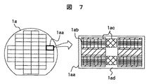
まず、本発明に係る異物等の欠陥を検査する被検査対象物1について図7および図8を用いて説明する。なお、詳細は特許3566589にて記載されているので、説明を省略する。
First, an
異物等の欠陥を検査する被検査対象物1としては、図7に示すように、メモリLSIからなるチップ1aaを所定の間隔で2次元に配列した半導体ウエハ1aがある。そして、メモリLSIからなるチップ1aaには、主としてメモリセル領域1abと、デコーダやコントロール回路等からなる周辺回路領域1acと、その他の領域1adとが形成されている。メモリセル領域1abは、メモリセルパターンを2次元に規則的に配列して(繰り返して)形成している。しかしながら、周辺回路領域1acは、パターンを2次元的に規則的に配列されていない非繰り返しパターンで形成されている。
As an
異物等の欠陥を検査する被検査対象物1としては、図8に示すように、マイコン等の
LSIからなるチップ1baを所定の間隔で2次元に配列した半導体ウエハ1bがある。そして、マイコン等のLSIからなるチップ1baは、主としてレジスタ群領域1bbと、メモリ部領域1bcと、CPUコア部領域1bdと、入出力部領域1beとで形成されている。なお、図8は、メモリ部領域1bcと、CPUコア部領域1bdと、入出力部領域1beとの配列を概念的に示したものである。レジスタ群領域1bbおよびメモリ部領域1bcは、2次元に規則的に配列して(繰り返して)形成している。CPUコア部領域1bdおよび入出力部領域1beは、パターンを非繰り返しで形成している。このように、異物等の欠陥を検査する被検査対象物1は、半導体ウエハを対象としても、チップは規則的に配列されているが、チップ内においては、最小線幅が領域毎に異なり、しかもパターンが繰り返し、非繰り返しでなど、様々な形態が考えられる。
As an
本発明に係る異物等の欠陥検査装置および方法は、このような被検査対象物1において、チップ内の非繰り返しパターン領域上の直線群からなるパターン(線状パターン)からの0次回折光を、対物レンズの入射瞳に入射させないようにすると共に非繰り返しパターン領域上に存在する異物等の欠陥によって生じる散乱光を受光することによって異物等の欠陥から信号を検出できるようにし、その欠陥の位置座標を算出できるようにした。
The defect inspection apparatus and method for foreign matter or the like according to the present invention provides a zero-order diffracted light from a pattern (linear pattern) consisting of straight lines on a non-repeated pattern region in a chip in such an
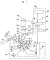
次に本発明に係る欠陥検査装置の第1の形態について図1,図2を用いて説明する。
異物等の欠陥検査装置の第1の実施の形態は、XYzステージ301,302,303,シータ(θ)ステージ304およびステージコントローラ305から構成されるステージ部300と、レーザ光源101,凹レンズ102および凸レンズ103より構成されるビームエキスパンダ、光学フィルタ群104およびミラー105で構成されるビーム整形部、素通しのガラス板と切換可能な光学分岐要素(またはミラー)106,円筒曲面を持つ照明レンズ107、およびミラー108,109より構成される3式のビームスポット結像部から構成される照明光学系100と、検出レンズ201,空間フィルタ202,結像レンズ203,ズームレンズ群204,TDIセンサ等の1次元検出器(イメージセンサ)205から構成される検出光学系,A/D変換部,遅延させることができるデータメモリ,チップ間の信号の差をとる差分処理回路,チップ間の差信号を一時記憶するメモリ,パターン閾値を設定する閾値算出処理部,比較回路より構成される信号処理系402,異物等の欠陥検出結果を記憶すると共に欠陥検出結果を出力する出力手段,モータ等の駆動,座標,センサを制御する演算処理系401,表示系403および入力系404より構成される制御系400とにより構成される。
Next, a first embodiment of the defect inspection apparatus according to the present invention will be described with reference to FIGS.
A first embodiment of a defect inspection apparatus for foreign matter or the like includes a
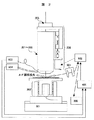
さらに図2に示すように、検出レンズに対して、オフアクシスの投受光結像系光路とポジションセンサを有するオートフォーカス系501,信号処理回路502,Z軸駆動系
303および305,センサZ方向駆動系206,気圧測定器504,温度計測定器503から本発明にかかわるユニットが構成されている。
Further, as shown in FIG. 2, an
なお、詳細は特許3566589にて記載されているので、説明を省略する。3つの照明光学系100は、レーザ光源101から射出された光を、凹レンズ102および凸レンズ103より構成されるビームエキスパンダ,円筒曲面を持つ照明レンズ107を通して、図6に示すようにスリット状のビーム3を平面的に3方向10,11,12から非検査対象基板(ウエハ)1に対して上記スリット状のビーム3の長手方向がチップの配列方向に向くように照明する構成となっている。なお、照明光として、スリット状のビーム3にするのは、異物等の欠陥の検査を高速化を実現したためである。即ち、図6に示すように、Xステージ301の走査方向のX方向およびYステージ302の走査方向のY方向に向けてチップ2を配列したウエハ1上に照明されるビーム3は、Yステージ302の走査方向Yに狭く、その垂直方向X(Xステージ301の走査方向)に広いスリットビームで照明する。そして、このスリット状のビーム3は、Y方向には、光源の像が結像するように、X方向には、平行光になるように照明される訳である。なお、3方向10,11,12からのスリット状のビーム3の照明は、ビームスプリッタまたはミラー106を同等厚さの素通しガラス板に切換ることにより個別、また2方向10,12からは同時に選択的に照明できる。
スリット状のビーム3の長手方向を、ウエハ(被検査基板)1に対してチップの配列方向に向け、且つYステージ302の走査方向Yに対して直角にすることにより、画像信号のチップ間比較を簡素化することができると共に欠陥位置座標の算出も容易に行うことができ、その結果異物等の欠陥検査の高速化を実現できるようにした。
Since details are described in Japanese Patent No. 3566589, description thereof will be omitted. The three illumination optical systems 100 pass the light emitted from the
By comparing the longitudinal direction of the slit-shaped
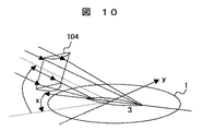
図9,図10に円錐形状および円筒曲面を持つ照明レンズ104を示す。なお、詳細は特許3566589にて記載されているので、説明を省略する円錐形状照明レンズ104は、シリンドリカルレンズの長手方向の位置で、焦点距離が異なり、直線的にこの焦点距離を変えたレンズである。この構成により、図9に示すように斜めから照明(α1,φ1の傾きを両立)しても、Y方向に絞り込み、X方向にコリメートされたスリット状のビーム3で照明することができる。即ち、この照明レンズ104により、図9(a)に示すようなX方向に平行光を有し、かつφ1=45度付近の照明を実現することができる。特に図11(a)に示すように、スリット状のビーム3をX方向に平行光にすることによって、主要な直線群がX方向およびY方向を向いた回路パターンから回折光パターンが得られ、空間フィルタ202によって遮光することができることになる。
次に、円筒曲面を持つ照明レンズ104は図10に示すスリット状ビーム3を形成することができる。
9 and 10 show an
Next, the
図11は、図1の3つのビームスポット結像部を有する照明光学系100を示す平面図である。レーザ光源101から出射したレーザビームをハーフミラー等の分岐光学要素
11で2つの光路に分岐し、一方はミラー111,112で反射させてミラー113で下方に向けて凹レンズ102に入射させることによって11の方向からの照明ビームを得ることができ、他方はハーフミラー等の分岐光学要素114へと進行する。該分岐光学要素114で分岐された一方は、ミラー115で反射させてミラー117で下方に向けて凹レンズ102に入射させることによって10の方向からの照明ビームを得ることができ、他方はミラー116で下方に向けて凹レンズ102に入射させることによって10の方向からの照明ビームを得ることができる。ところで、11の方向からのみ照明する場合には、分岐光学要素110からミラー要素118に切り換えることによって実現することができる。また、10および12の方向からのみ照明する場合には、光路から分岐光学要素110を退出させるかまたは素通りの光学要素に切り換えることによって実現することができる。また、10および12方向からの照明の内、例えば12方向からのみ照明する場合には、分岐光学要素114からミラー要素119に切り換えることによって実現することができる。
FIG. 11 is a plan view showing an illumination optical system 100 having the three beam spot imaging units in FIG. A laser beam emitted from the
なお、レーザ光源101として、分岐する関係で高出力のYAGレーザの第3高調波
THG,波長355nmを用いるのがよいが、必ずしも355nmである必要はない。また、レーザ光源101として、YAGTHGである必要もない。すなわち、レーザ光源
101として、Arレーザ,窒素レーザ,He−Cdレーザ,エキシマレーザ等他の光源であっても良い。
As the
検出光学系200は、ウエハ1から射出した光を、検出レンズ(対物レンズ)201,繰り返しパターンからの反射回折光によるフーリエ変換像を遮光する空間フィルタ202,結像レンズ203,TDIセンサ等の1次元検出器205で検出するように構成される。空間フィルタ202は、繰り返しパターンからの反射回折光によるフーリエ変換像を遮光すべく、対物レンズ201の空間周波数領域、即ちフーリエ変換(射出瞳に相当する。)の結像位置に置かれている。ここで、図7に示すウエハ1上の照明エリア3が、リレーレンズを構成する対物レンズ201,結像203により、検出器205上に結像される。4は、TDIセンサ等の1次元検出器205の受光エリアを示すものである。
The detection
前述したように様々な形態の回路パターンが形成されたウエハ(基板)1に対してスリット状のビーム3が照明されると、この反射回折光(あるいは散乱光)が、ウエハの表面、回路パターン、異物等の欠陥から射出することになる。この射出した光は、検出レンズ201,空間フィルタ202,結像レンズ203を通して、検出器205で受光されて光電変換される。しかし、レーザ光源101等の照明光学系から照射されるビーム光束の照度(パワー)はNDフィルタ104またはレーザパワー制御して変えることにより、ダイナミックレンジを変えることができる。
面の円周上になる。
As described above, when the slit-shaped
On the circumference of the surface.
また、被検査基板(ウエハ)1に対して、配線等の間の凹部に入り込んだ異物あるいは欠陥、エッチ残り等を検査する必要がある。しかしながら、被検査基板1上には非繰り返しパターンが存在し、該非繰り返しパターンからの0次の回折光が対物レンズ201に入射しないようにするために、上記に説明したように、Y軸に対してほぼ45度の角度の方向10,12からX方向に長手方向を有するスリット状のビーム3を基板1上に照明したのでは、凸部である配線等が邪魔をして凹部を十分に照明することが難しくなる。
Further, it is necessary to inspect the inspected substrate (wafer) 1 for a foreign matter or a defect that has entered a recess between wirings, an etching residue, and the like. However, there is a non-repeating pattern on the
そこで、配線パターンが多くの場合、直角,平行方向に形成されていることから、Y軸に平行な方向11から基板1に対してスリット状のビーム3を照明することによって、配線等の間の凹部を十分照明することが可能となる。特に、メモリLSIの配線パターンは数mmの長さの直線パターンで有ることが多く、この方向11からの照明により検査可能になることが多い。また、パターンにより、90度方向の場合は、ウエハを90度回転させて検査するか、照明方向をX方向にすることにより検査可能となる。
Therefore, in many cases, since the wiring pattern is formed in a right angle and parallel direction, the slit-
次に空間フィルタ202について説明する。チップ2内には、メモリLSI1aaにおけるメモリセル領域1abや、マイコン等のLSI1baにおけるレジスタ群領域1bbおよびメモリ部領域1bcのように、繰り返しパターンが存在することになり、この繰り返しパターンからの回折光縞(回折干渉光縞)を空間フィルタ202によって遮光することが要求される。要するに、チップ2内には、繰り返しパターンと非繰り返しパターンとパターンなしとが混在することになり、しかも夫々線幅も異なることになるので、通常は、頻度の多い例えば繰り返しパターンからの回折光を消去するように空間フィルタ202の遮光パターンが設定されることになる。また、空間フィルタ202として、特開平5−218163号公報および特開平6−258239号公報に記載されているように.遮光パターンを変更できるものを用いれば、チップ2内の回路パターンに応じて変更させればよい。また、空間フィルタ202として、遮光パターンが異なるものを用意しておいて、チップ2内の回路パターンに応じて切り換えてもよい。しかしながら、方向11からスリット状のビーム3を照明した場合、0次回折光を空間フィルタ202によって遮光して消去する必要が生じることになる。この際、当然高次の回折光を空間フィルタ202によって遮光して消去することも可能である。以上、被検査基板1上のチップ2内に存在する繰返しおよび非繰り返しパターンの場合における回折光の消去方法について説明した。
Next, the
次に、検出しようとする異物等の欠陥サイズに応じた検出感度調整について説明する。即ち、TDIセンサ等の1次元検出器(イメージセンサ)205の被検査対象物1上での検出画素サイズを小さくすると、スループットは落ちるものの、検出感度の向上が見込める。そこで、0.1μm 程度以下の異物等の欠陥を検出する際、画素サイズを小さくする検出光学系200に切り替えて用いると良い。具体的には、TDIセンサ等の画素についてウエハ1上での像のサイズが可変となるような3種類の検出光学系200を持つと良い。この構成の実現方法として、レンズ群204を切り替える。この際、ウエハ1から、
TDIセンサ等の1次元検出器205までの光路長を変えずに済むように、レンズの構成を設計しておくと良い。もちろん、このような設計が難しい場合、レンズの切り替えに併せて、センサまでの距離を変えられるような機構を用いても良い。また、センサ自体の画素サイズを変えたものを切り替えても良い。
Next, detection sensitivity adjustment according to the defect size of a foreign substance or the like to be detected will be described. That is, when the detection pixel size on the
It is preferable to design the lens configuration so that the optical path length to the one-
以下に本発明の詳細な実施形態を図2にて説明する。本発明では環境が変化したときに発生する結像位置ずれを補正するためのデータを図2に示す温度測定器503、及び気圧測定器504で測定する。データは、通信ケーブル経由で制御CPU部401に読み込まれる。CPUは図5の温度気圧変位を被検査基板高さ補正量に換算するテーブルを用いて補正値を算出する。その結果はオートフォーカス系の信号処理回路502に合焦点位置に対してオフセットの発生を指示する。そのオフセット量に対する偏差をなくするように
502はZステージを駆動させて被検査基板の高さを修正する。その結果図4に示すように、センサ高さを固定した場合に、被検査基板の高さを変えて被検査基板上の欠陥がセンサにデフォーカスにならないように結像させることができる。被検査基板の高さを補正した場合は別途照明系のスポット3の位置がずれるため、自動的にセンタにスポット位置を補正する機能が必要となる。
A detailed embodiment of the present invention will be described below with reference to FIG. In the present invention, data for correcting an imaging position shift that occurs when the environment changes is measured by the
上記とは逆に結像位置ずれをセンサの高さを変更して補正することが可能である。この場合前述の照明系のスポット3の位置を自動的にセンタに補正する機能が不要となる。
Contrary to the above, it is possible to correct the imaging position deviation by changing the height of the sensor. In this case, the function of automatically correcting the position of the
温度気圧の測定箇所は装置内、装置外でも可能であるが、前述した環境による結像位置ずれのメカニズムから検査レンズ、特に対物レンズ201の相対屈折率変化が結像位置ずれに大きく影響することから本発明では気圧はレンズ近傍、温度は対物レンズ表面を計測することを特徴としている。
The measurement location of temperature and pressure can be inside or outside the device, but due to the mechanism of the imaging position shift due to the environment described above, the change in the relative refractive index of the inspection lens, particularly the
1…被検査基板(ウエハ)2…チップ、3…スリット状ビーム(照明領域)、4…TDIセンサ等のイメージセンサの検出領域、100…照明光学系、101…レーザ光源、102…凹レンズ、103…凸レンズ、104…NDフィルタおよび波長板、110…0度照明ビームスポット結像部、120…45度照明ビームスポット結像部(11方向)、130…45度照明ビームスポット結像部(12方向)、200…上方検出光学系、201…対物レンズ(検出レンズ)、202…空間フィルタ、203…結像レンズ、204…ズームレンズ群、205…TDIセンサ等の1次元検出器、206…センサZ駆動機構、207…空間フィルタ制御、208…ズームレンズ制御、300…ステージ系、301〜304…XYZΘステージ、305…ステージ制御、400…演算処理回路(信号処理系)、
401…制御CPU部、402…信号処理部、403…表示部、404…入力部、500…斜方検出系、501…オートフォーカスユニット、502…信号処理回路、503…温度計測定器、504…気圧測定器。
DESCRIPTION OF
401: control CPU section 402: signal processing section 403: display section 404: input section 500:
Claims (9)
オートフォーカスの照明光は前記検出光学系の検出レンズに干渉しない空間に照明光路を有し、暗視野照明となるように被検査基板上の投影し、反射光を対向するポジションセンサに結像させる構成を備えたことを特徴とする欠陥検査装置。 The defect inspection apparatus according to claim 1 or 2,
The autofocus illumination light has an illumination optical path in a space that does not interfere with the detection lens of the detection optical system, is projected onto the inspected substrate so as to be dark field illumination, and the reflected light is imaged on the opposing position sensor. A defect inspection apparatus characterized by comprising a configuration.
前記検出光学系は拡大系レンズを有し、欠陥の散乱光を高NAで取り込み、センサに拡大投影させることによって、より微小な欠陥,解像限界以下の欠陥を検出可能とすることを特徴とする欠陥検査装置。 In the defect inspection apparatus in any one of Claims 1-3,
The detection optical system has a magnifying lens, and can detect a smaller defect and a defect below the resolution limit by capturing the scattered light of the defect with a high NA and projecting it on a sensor. Defect inspection equipment.
温度及び気圧の変化に対して前記検出光学系のセンサの高さまたは被検査基板高さを補正する結像位置補正機構を備えたことを特徴とする欠陥検査装置。 In the defect inspection apparatus in any one of Claims 1-5,
A defect inspection apparatus comprising an imaging position correction mechanism for correcting the height of a sensor of the detection optical system or the height of a substrate to be inspected with respect to changes in temperature and atmospheric pressure.
結像位置を補正するために、センサを上下させるZ機構、または被検査基板の高さを変更するステージZ機構を備えたことを特徴とする欠陥検査装置。 The defect inspection apparatus according to claim 6,
A defect inspection apparatus comprising a Z mechanism for moving a sensor up and down or a stage Z mechanism for changing a height of a substrate to be inspected in order to correct an imaging position.
温度のセンサ部分を検査レンズ表面および気圧測定口を検査レンズ近傍に設置したことを特徴とする欠陥検査装置。 The defect inspection apparatus according to claim 5,
A defect inspection apparatus characterized in that a temperature sensor part is installed on the surface of an inspection lens and an air pressure measurement port is provided in the vicinity of the inspection lens.
事前に温度,気圧の少なくともいずれかと、補正量の相関をテーブルデータとして記憶する記憶手段を備え、該記憶手段に記憶されたテーブルデータに基づき、結像位置補正をリアルタイムに実行する機構を備えたことを特徴とする欠陥検査装置。
In the defect inspection apparatus in any one of Claims 1-8,
A storage unit that stores a correlation between at least one of temperature and atmospheric pressure and a correction amount as table data in advance, and a mechanism that executes imaging position correction in real time based on the table data stored in the storage unit A defect inspection apparatus characterized by that.
Priority Applications (4)
| Application Number | Priority Date | Filing Date | Title |
|---|---|---|---|
| JP2006068479A JP2007248086A (en) | 2006-03-14 | 2006-03-14 | Flaw inspection device |
| US11/717,651 US7535561B2 (en) | 2006-03-14 | 2007-03-14 | Defect inspecting apparatus |
| US12/428,065 US7733475B2 (en) | 2006-03-14 | 2009-04-22 | Defect inspecting apparatus |
| US12/774,379 US8134701B2 (en) | 2006-03-14 | 2010-05-05 | Defect inspecting method and apparatus |
Applications Claiming Priority (1)
| Application Number | Priority Date | Filing Date | Title |
|---|---|---|---|
| JP2006068479A JP2007248086A (en) | 2006-03-14 | 2006-03-14 | Flaw inspection device |
Related Child Applications (1)
| Application Number | Title | Priority Date | Filing Date |
|---|---|---|---|
| JP2011167978A Division JP2012013707A (en) | 2011-08-01 | 2011-08-01 | Defect inspection device |
Publications (2)
| Publication Number | Publication Date |
|---|---|
| JP2007248086A true JP2007248086A (en) | 2007-09-27 |
| JP2007248086A5 JP2007248086A5 (en) | 2008-07-10 |
Family
ID=38517426
Family Applications (1)
| Application Number | Title | Priority Date | Filing Date |
|---|---|---|---|
| JP2006068479A Pending JP2007248086A (en) | 2006-03-14 | 2006-03-14 | Flaw inspection device |
Country Status (2)
| Country | Link |
|---|---|
| US (3) | US7535561B2 (en) |
| JP (1) | JP2007248086A (en) |
Cited By (9)
| Publication number | Priority date | Publication date | Assignee | Title |
|---|---|---|---|---|
| JP2009150725A (en) * | 2007-12-19 | 2009-07-09 | Hitachi High-Technologies Corp | Defect inspection system |
| JP2010145735A (en) * | 2008-12-18 | 2010-07-01 | Mitsubishi Heavy Ind Ltd | Imaging apparatus and imaging method |
| WO2010084884A1 (en) * | 2009-01-26 | 2010-07-29 | 株式会社日立ハイテクノロジーズ | Dark-field defect inspection method, dark-field defect inspection device, aberration analysis method and aberration analysis device |
| JP2011009554A (en) * | 2009-06-26 | 2011-01-13 | Fujitsu Semiconductor Ltd | Method and device for inspecting defect |
| WO2013046836A1 (en) * | 2011-09-28 | 2013-04-04 | 株式会社日立ハイテクノロジーズ | Defect inspection method and defect inspection device |
| KR101516937B1 (en) | 2012-06-27 | 2015-05-15 | 가부시키가이샤 뉴플레어 테크놀로지 | Inspection method and inspection apparatus |
| US9140654B2 (en) | 2013-04-26 | 2015-09-22 | Nuflare Technology, Inc. | Inspection apparatus |
| JP2018530912A (en) * | 2015-08-28 | 2018-10-18 | ケーエルエー−テンカー コーポレイション | Method for optimizing imaging performance for semiconductor wafer inspection |
| WO2020066503A1 (en) | 2018-09-27 | 2020-04-02 | 富士フイルム株式会社 | Observation system and observation method and observation system control program |
Families Citing this family (14)
| Publication number | Priority date | Publication date | Assignee | Title |
|---|---|---|---|---|
| JP2007248086A (en) * | 2006-03-14 | 2007-09-27 | Hitachi High-Technologies Corp | Flaw inspection device |
| US20080024772A1 (en) * | 2006-07-26 | 2008-01-31 | Seagate Technology Llc | Particle removal tool with integrated defect detection/analysis capability |
| JP4696099B2 (en) * | 2007-08-07 | 2011-06-08 | 日立オムロンターミナルソリューションズ株式会社 | Display image converter |
| US8705050B2 (en) * | 2010-10-06 | 2014-04-22 | International Business Machines Corporation | Providing thermal compensation for topographic measurement at an elevated temperature using a non-contact vibration transducer |
| KR101245530B1 (en) * | 2011-05-26 | 2013-03-21 | 주식회사 탑 엔지니어링 | Optical inspection apparatus and array test apparatus having the same |
| JPWO2013099468A1 (en) | 2011-12-27 | 2015-04-30 | 株式会社日立ハイテクノロジーズ | Inspection device |
| JP6251559B2 (en) * | 2013-02-28 | 2017-12-20 | 株式会社ニューフレアテクノロジー | Sample support device |
| CN107971637B (en) * | 2017-11-29 | 2019-12-03 | 武汉华夏精冲技术有限公司 | Laser marking device with detection function |
| JP6988592B2 (en) * | 2018-03-13 | 2022-01-05 | オムロン株式会社 | Image inspection equipment, image inspection method and image inspection program |
| CN110220615B (en) * | 2019-05-20 | 2020-11-03 | 广州亚禾电子科技有限公司 | Continuous monitoring method and system for reasonability of layout position of machine room heating equipment |
| US11581692B2 (en) * | 2019-06-18 | 2023-02-14 | KLA Corp. | Controlling pressure in a cavity of a light source |
| CN110160472B (en) * | 2019-06-27 | 2021-06-11 | 南京涵铭置智能科技有限公司 | Plate use standard detection device and detection method thereof |
| CN116754578B (en) * | 2023-08-18 | 2023-11-03 | 国镓芯科(成都)半导体科技有限公司 | Detection system for wafer scratch and detection method of system |
| CN116990320B (en) * | 2023-09-27 | 2023-12-19 | 江西驰宇光电科技发展有限公司 | Dark field imaging method and device for defect detection |
Citations (7)
| Publication number | Priority date | Publication date | Assignee | Title |
|---|---|---|---|---|
| JPH04350613A (en) * | 1991-05-28 | 1992-12-04 | Hitachi Ltd | Image recognizing device |
| JPH0547629A (en) * | 1991-08-09 | 1993-02-26 | Canon Inc | Manufacturing method of semiconductor device and projection aligner using the same |
| JPH09134948A (en) * | 1995-11-07 | 1997-05-20 | Hitachi Electron Eng Co Ltd | Device for positioning work table |
| JP2002090311A (en) * | 2000-09-18 | 2002-03-27 | Hitachi Ltd | Defect inspection device |
| JP2004061289A (en) * | 2002-07-29 | 2004-02-26 | Toshiba Corp | Pattern inspecting apparatus |
| JP3566589B2 (en) * | 1998-07-28 | 2004-09-15 | 株式会社日立製作所 | Defect inspection apparatus and method |
| JP2006030021A (en) * | 2004-07-16 | 2006-02-02 | Nikon Corp | Position detection apparatus and position detection method |
Family Cites Families (26)
| Publication number | Priority date | Publication date | Assignee | Title |
|---|---|---|---|---|
| JPH0781956B2 (en) | 1985-10-16 | 1995-09-06 | 株式会社日立製作所 | Foreign object detection device on semiconductor substrate |
| JP2609594B2 (en) | 1986-11-28 | 1997-05-14 | 株式会社日立製作所 | Defect inspection equipment |
| JPH0786465B2 (en) | 1987-10-30 | 1995-09-20 | 株式会社日立製作所 | Foreign object detection method and apparatus |
| US4877326A (en) | 1988-02-19 | 1989-10-31 | Kla Instruments Corporation | Method and apparatus for optical inspection of substrates |
| US6411377B1 (en) | 1991-04-02 | 2002-06-25 | Hitachi, Ltd. | Optical apparatus for defect and particle size inspection |
| JPH05218163A (en) | 1991-12-11 | 1993-08-27 | Hitachi Ltd | Method and device for inspecting foreing matter |
| US5473426A (en) * | 1993-03-05 | 1995-12-05 | Nikon Corporation | Defect inspection apparatus |
| JP3275425B2 (en) | 1993-03-09 | 2002-04-15 | 株式会社日立製作所 | Defect detection apparatus and method |
| JP3435187B2 (en) | 1993-05-12 | 2003-08-11 | 株式会社日立製作所 | Defect inspection method and apparatus |
| JP3445045B2 (en) * | 1994-12-29 | 2003-09-08 | キヤノン株式会社 | Projection exposure apparatus and device manufacturing method using the same |
| JP3593375B2 (en) | 1995-02-07 | 2004-11-24 | 株式会社日立製作所 | Micro defect detection method and device |
| JP3379855B2 (en) | 1995-03-30 | 2003-02-24 | 株式会社日立製作所 | Foreign matter inspection method and apparatus |
| JP3639636B2 (en) * | 1995-04-25 | 2005-04-20 | 株式会社ルネサステクノロジ | Semiconductor wafer failure analysis apparatus and failure analysis method |
| US5694214A (en) * | 1996-01-08 | 1997-12-02 | Hitachi Electronics Engineering Co., Ltd. | Surface inspection method and apparatus |
| US6608676B1 (en) | 1997-08-01 | 2003-08-19 | Kla-Tencor Corporation | System for detecting anomalies and/or features of a surface |
| US6324298B1 (en) * | 1998-07-15 | 2001-11-27 | August Technology Corp. | Automated wafer defect inspection system and a process of performing such inspection |
| JP3904796B2 (en) | 2000-03-14 | 2007-04-11 | 株式会社日立製作所 | Foreign object or defect inspection apparatus, and foreign object or defect inspection method |
| JP3793668B2 (en) | 1999-08-24 | 2006-07-05 | 株式会社日立製作所 | Foreign object defect inspection method and apparatus |
| JP2003066341A (en) * | 2001-08-28 | 2003-03-05 | Nec Corp | Reticle inspection device |
| JP4154978B2 (en) | 2002-09-27 | 2008-09-24 | トヨタ自動車株式会社 | Prediction method of gas adsorption capacity of carbon nanotubes with other elements |
| JP4183492B2 (en) | 2002-11-27 | 2008-11-19 | 株式会社日立製作所 | Defect inspection apparatus and defect inspection method |
| US7223503B2 (en) * | 2003-12-30 | 2007-05-29 | Taiwan Semiconductor Manufacturing Company | Method for repairing opaque defects on semiconductor mask reticles |
| JP2007071803A (en) * | 2005-09-09 | 2007-03-22 | Hitachi High-Technologies Corp | Defect observation method and its apparatus |
| JP2007248086A (en) * | 2006-03-14 | 2007-09-27 | Hitachi High-Technologies Corp | Flaw inspection device |
| US8102522B2 (en) * | 2006-06-30 | 2012-01-24 | Hitachi High-Technologies Corporation | Inspection apparatus and inspection method |
| JP5147202B2 (en) * | 2006-06-30 | 2013-02-20 | 株式会社日立ハイテクノロジーズ | Optical defect inspection system |
-
2006
- 2006-03-14 JP JP2006068479A patent/JP2007248086A/en active Pending
-
2007
- 2007-03-14 US US11/717,651 patent/US7535561B2/en not_active Expired - Fee Related
-
2009
- 2009-04-22 US US12/428,065 patent/US7733475B2/en not_active Expired - Fee Related
-
2010
- 2010-05-05 US US12/774,379 patent/US8134701B2/en active Active
Patent Citations (7)
| Publication number | Priority date | Publication date | Assignee | Title |
|---|---|---|---|---|
| JPH04350613A (en) * | 1991-05-28 | 1992-12-04 | Hitachi Ltd | Image recognizing device |
| JPH0547629A (en) * | 1991-08-09 | 1993-02-26 | Canon Inc | Manufacturing method of semiconductor device and projection aligner using the same |
| JPH09134948A (en) * | 1995-11-07 | 1997-05-20 | Hitachi Electron Eng Co Ltd | Device for positioning work table |
| JP3566589B2 (en) * | 1998-07-28 | 2004-09-15 | 株式会社日立製作所 | Defect inspection apparatus and method |
| JP2002090311A (en) * | 2000-09-18 | 2002-03-27 | Hitachi Ltd | Defect inspection device |
| JP2004061289A (en) * | 2002-07-29 | 2004-02-26 | Toshiba Corp | Pattern inspecting apparatus |
| JP2006030021A (en) * | 2004-07-16 | 2006-02-02 | Nikon Corp | Position detection apparatus and position detection method |
Cited By (17)
| Publication number | Priority date | Publication date | Assignee | Title |
|---|---|---|---|---|
| JP2009150725A (en) * | 2007-12-19 | 2009-07-09 | Hitachi High-Technologies Corp | Defect inspection system |
| JP2010145735A (en) * | 2008-12-18 | 2010-07-01 | Mitsubishi Heavy Ind Ltd | Imaging apparatus and imaging method |
| KR101304615B1 (en) * | 2009-01-26 | 2013-09-05 | 가부시키가이샤 히다치 하이테크놀로지즈 | Dark-field defect inspection method, dark-field defect inspection device, aberration analysis method and aberration analysis device |
| WO2010084884A1 (en) * | 2009-01-26 | 2010-07-29 | 株式会社日立ハイテクノロジーズ | Dark-field defect inspection method, dark-field defect inspection device, aberration analysis method and aberration analysis device |
| JP2010190885A (en) * | 2009-01-26 | 2010-09-02 | Hitachi High-Technologies Corp | Dark field defect inspection method, dark field defect inspection device, aberration analysis method, and aberration analyzer |
| US8681328B2 (en) | 2009-01-26 | 2014-03-25 | Hitachi High-Technologies Corporation | Dark-field defect inspecting method, dark-field defect inspecting apparatus, aberration analyzing method, and aberration analyzing apparatus |
| JP2011009554A (en) * | 2009-06-26 | 2011-01-13 | Fujitsu Semiconductor Ltd | Method and device for inspecting defect |
| JP2013072750A (en) * | 2011-09-28 | 2013-04-22 | Hitachi High-Technologies Corp | Defect checking method and defect checking apparatus |
| WO2013046836A1 (en) * | 2011-09-28 | 2013-04-04 | 株式会社日立ハイテクノロジーズ | Defect inspection method and defect inspection device |
| US9291574B2 (en) | 2011-09-28 | 2016-03-22 | Hitachi High-Technologies Corporation | Defect inspection method and defect inspection device |
| US9470640B2 (en) | 2011-09-28 | 2016-10-18 | Hitachi High-Technologies Corporation | Defect inspection method and defect inspection device |
| KR101516937B1 (en) | 2012-06-27 | 2015-05-15 | 가부시키가이샤 뉴플레어 테크놀로지 | Inspection method and inspection apparatus |
| US9116136B2 (en) | 2012-06-27 | 2015-08-25 | Nuflare Technology, Inc | Inspection method and system |
| US9140654B2 (en) | 2013-04-26 | 2015-09-22 | Nuflare Technology, Inc. | Inspection apparatus |
| JP2018530912A (en) * | 2015-08-28 | 2018-10-18 | ケーエルエー−テンカー コーポレイション | Method for optimizing imaging performance for semiconductor wafer inspection |
| WO2020066503A1 (en) | 2018-09-27 | 2020-04-02 | 富士フイルム株式会社 | Observation system and observation method and observation system control program |
| JPWO2020066503A1 (en) * | 2018-09-27 | 2021-08-30 | 富士フイルム株式会社 | Observation device and method and observation device control program |
Also Published As
| Publication number | Publication date |
|---|---|
| US20100214561A1 (en) | 2010-08-26 |
| US20090207405A1 (en) | 2009-08-20 |
| US20070216896A1 (en) | 2007-09-20 |
| US7733475B2 (en) | 2010-06-08 |
| US8134701B2 (en) | 2012-03-13 |
| US7535561B2 (en) | 2009-05-19 |
Similar Documents
| Publication | Publication Date | Title |
|---|---|---|
| JP2007248086A (en) | Flaw inspection device | |
| JP4713185B2 (en) | Foreign object defect inspection method and apparatus | |
| JP5303217B2 (en) | Defect inspection method and defect inspection apparatus | |
| JP5469839B2 (en) | Device surface defect inspection apparatus and method | |
| JP3258385B2 (en) | Optical board inspection system | |
| US7847927B2 (en) | Defect inspection method and defect inspection apparatus | |
| US7872743B2 (en) | Defect inspection system | |
| JP5112650B2 (en) | Method and system for determining drift of the position of a light beam relative to a chuck | |
| JP5297930B2 (en) | Defect inspection apparatus and method | |
| JP2007107960A (en) | Flaw inspection device | |
| JP2008051666A (en) | Flaw inspection device | |
| JP5276833B2 (en) | Defect inspection method and defect inspection apparatus | |
| JP2008216219A (en) | Illuminating device, defect inspection device using the same and defect inspection method, and height measuring device and height measuring method | |
| US9151719B2 (en) | Inspection apparatus | |
| JP2011180145A (en) | Flaw inspection device | |
| JP2012013707A (en) | Defect inspection device | |
| JP5123003B2 (en) | Inspection apparatus and inspection method | |
| JPH08304296A (en) | Method and system for detecting defect of foreign matter | |
| JP5301293B2 (en) | Defect inspection apparatus and method | |
| JPH0682381A (en) | Foreign matter inspection device | |
| JPS60135809A (en) | Flaw detection apparatus | |
| JP2012163422A (en) | Inspection device |
Legal Events
| Date | Code | Title | Description |
|---|---|---|---|
| A521 | Written amendment |
Free format text: JAPANESE INTERMEDIATE CODE: A523 Effective date: 20080421 |
|
| A621 | Written request for application examination |
Free format text: JAPANESE INTERMEDIATE CODE: A621 Effective date: 20080421 |
|
| A521 | Written amendment |
Free format text: JAPANESE INTERMEDIATE CODE: A523 Effective date: 20080421 |
|
| A977 | Report on retrieval |
Free format text: JAPANESE INTERMEDIATE CODE: A971007 Effective date: 20100929 |
|
| A131 | Notification of reasons for refusal |
Free format text: JAPANESE INTERMEDIATE CODE: A131 Effective date: 20101005 |
|
| A521 | Written amendment |
Free format text: JAPANESE INTERMEDIATE CODE: A523 Effective date: 20101130 |
|
| A131 | Notification of reasons for refusal |
Free format text: JAPANESE INTERMEDIATE CODE: A131 Effective date: 20110614 |
|
| A521 | Written amendment |
Free format text: JAPANESE INTERMEDIATE CODE: A523 Effective date: 20110801 |
|
| A131 | Notification of reasons for refusal |
Free format text: JAPANESE INTERMEDIATE CODE: A131 Effective date: 20110906 |
|
| A02 | Decision of refusal |
Free format text: JAPANESE INTERMEDIATE CODE: A02 Effective date: 20120110 |