JP2007237671A - Method for manufacturing inkjet recording head - Google Patents
Method for manufacturing inkjet recording head Download PDFInfo
- Publication number
- JP2007237671A JP2007237671A JP2006065966A JP2006065966A JP2007237671A JP 2007237671 A JP2007237671 A JP 2007237671A JP 2006065966 A JP2006065966 A JP 2006065966A JP 2006065966 A JP2006065966 A JP 2006065966A JP 2007237671 A JP2007237671 A JP 2007237671A
- Authority
- JP
- Japan
- Prior art keywords
- recording head
- etching
- film
- substrate
- ink
- Prior art date
- Legal status (The legal status is an assumption and is not a legal conclusion. Google has not performed a legal analysis and makes no representation as to the accuracy of the status listed.)
- Withdrawn
Links
Images


Abstract
Description
本発明は、液体に外部からエネルギーを加えることによって、所望の液体を吐出するインクジェット記録ヘッド、およびインクジェット記録ヘッドの製造方法に関する。 The present invention relates to an inkjet recording head that discharges a desired liquid by applying energy to the liquid from the outside, and a method for manufacturing the inkjet recording head.
熱等のエネルギーをインクに与えることで、気泡の発生を促し、この体積変化を利用して吐出口からインクを吐出し、これを記録媒体上に付着させて画像形成を行うインクジェット記録方法が知られている。インクジェット方式の中で、基板に対し垂直にインクを吐出するサイドシューター型(特許文献1)が提案されている。また、このヘッドの製法として、犠牲層を用いてインク供給口の形状を成型する方法(特許文献2)が開示されている。 There is known an ink jet recording method in which the generation of bubbles is promoted by applying energy such as heat to the ink, the ink is ejected from the ejection port using this volume change, and this is deposited on the recording medium to form an image. It has been. Among ink jet systems, a side shooter type (Patent Document 1) that ejects ink perpendicular to a substrate has been proposed. Further, as a method for manufacturing this head, a method (Patent Document 2) is disclosed in which the shape of the ink supply port is molded using a sacrificial layer.
これは、シリコン基板上に酸化シリコン膜あるいは窒化シリコン膜を形成し、前記酸化シリコン膜あるいは窒化シリコン膜上にインク吐出圧発生素子を形成し、前記シリコン基板表面にエッチング液に侵されやすい材料で薄膜を堆積しインク吐出口の形状にパターン(エッチング犠牲層)を形成し、さらに前記吐出口の形状のパターン上にエッチングストップ層を形成し、前記シリコン基板表面にインク吐出口部を形成し、前記酸化シリコン膜あるいは窒化シリコン膜形成面の裏面に開口部を設け、異方性エッチングによりインク供給口となる部分のシリコンを除去し、インク供給口部に残ったエッチングストップ層の酸化シリコン膜あるいは窒化シリコン膜またはその混合物を除去する工程によって形成されていた。
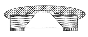
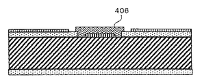
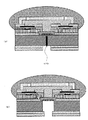
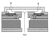
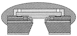
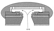
従来のサイドシューター型のインクジェット記録ヘッドでは、エッチング犠牲層パターニング時に、断面が垂直になるような形状に形成していた。その上にエッチングストップ層を堆積すると、図5のようにエッチング犠牲層の肩に局所的にひずみの集中する部分が発生していた。そのため、異方性エッチングでシリコンウエハをエッチングして、犠牲層を取り去ると、図6のようにエッチングストップ層に亀裂が入り、エッチング液が進入して、インク流路形成樹脂204やノズル形成樹脂205が変質、変形してしまうことがあった。 In the conventional side shooter type ink jet recording head, the cross section is formed in a vertical shape when the etching sacrificial layer is patterned. When an etching stop layer was deposited thereon, a portion where strain was locally concentrated on the shoulder of the etching sacrificial layer was generated as shown in FIG. Therefore, when the silicon wafer is etched by anisotropic etching and the sacrificial layer is removed, the etching stop layer cracks as shown in FIG. 205 may be altered or deformed.
上記のような問題点は、シリコン基板上に畜熱層として酸化シリコン膜あるいは窒化シリコン膜などの絶縁膜を形成する工程、前記膜上にインク吐出圧発生素子を形成する工程、前記シリコン基板表面にエッチング液に侵されやすい材料で薄膜を堆積しインク吐出口の形状にパターンを形成する工程、前記吐出口の形状のパターン上にエッチングストップ層を形成する工程、前記酸化シリコン膜あるいは窒化シリコン膜が形成された裏面に開口部を設け、異方性エッチングによりインク供給口となる部分のシリコンを除去する工程、インク供給口部に残ったエッチングストップ層の酸化シリコン膜あるいは窒化シリコン膜またはその混合物を除去する工程を少なくとも含むインクジェット記録ヘッドの製造方法であって、前記基板表面の吐出口の形状の薄膜パターンのパターンのエッジ部が基板表面に対して75度以下の傾きを持っていることを特徴とすることを特徴とするインクジェット記録ヘッドの製造方法によって解決される。 The above-mentioned problems include a step of forming an insulating film such as a silicon oxide film or a silicon nitride film as a livestock heat layer on a silicon substrate, a step of forming an ink discharge pressure generating element on the film, a surface of the silicon substrate A step of depositing a thin film with a material susceptible to etching liquid to form a pattern in the shape of the ink discharge port, a step of forming an etching stop layer on the pattern of the discharge port shape, the silicon oxide film or the silicon nitride film An opening is formed on the back surface on which the ink is formed and the silicon serving as the ink supply port is removed by anisotropic etching, the silicon oxide film or silicon nitride film of the etching stop layer remaining in the ink supply port, or a mixture thereof A method of manufacturing an ink jet recording head including at least a step of removing ink, wherein the substrate surface is discharged Edge portion of the pattern of the thin film pattern of the shape is solved by the manufacturing method of the ink jet recording head is characterized in that characterized in that with an inclination of less than 75 degrees with respect to the substrate surface.
[作用]
エッチング犠牲層にテーパーを持たせることによって、その上に堆積されるエッチングストップ層の薄膜の、犠牲層の肩部での応力集中を緩和し、異方性エッチングにより下部の犠牲層が除去された後に、エッチングストップ層に亀裂が発生することを防止する。
[Action]
By giving the etching sacrificial layer a taper, the stress concentration at the shoulder of the sacrificial layer of the thin film of the etching stop layer deposited thereon was eased, and the lower sacrificial layer was removed by anisotropic etching. Later, cracks are prevented from occurring in the etching stop layer.
最適なテーパー角は、犠牲層膜厚と犠牲層材質、エッチングストップ層の膜厚と内部応力によって異なるが、おおむね犠牲層側面の角度が浅い方がエッチングストップ層の亀裂の発生確率は低下する。 The optimum taper angle varies depending on the sacrificial layer thickness and sacrificial layer material, the thickness of the etching stop layer, and the internal stress, but the probability of occurrence of cracks in the etching stop layer generally decreases when the angle of the side surface of the sacrificial layer is shallow.
[実験]
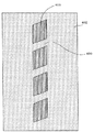
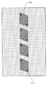
以下に、本発明に関わる実験について述べる。図1は実験に用いたサンプルの断面構造を示したものである。5インチΦ、厚さ625μmのSi(100)ウエハ101の表面にAlCu膜を3000Å堆積し平面図3のようにパターニングして犠牲層102とした。犠牲層の形状は長方形で、幅150μm、長さ2mmとした。その上にプラズマCVDによるSiN膜を6000Å堆積してエッチングストップ層103とした。この時のSiN膜の成膜条件は、SiH4/NH3/N2=500/1500/6300sccm、圧力150mtorr、基板温度380℃、RF 1700Wであった。単体の膜で測った膜応力は1.5×10exp−9dyne/cmであった。また基板の裏面には、熱酸化膜を平面図4のようにパターニングした異方性エッチング用パターンが形成してある。基板表面には耐アルカリ性のレジスト(OBC 東京応化製)106が塗布してある。
[Experiment]
Hereinafter, experiments related to the present invention will be described. FIG. 1 shows a cross-sectional structure of a sample used in the experiment. A
犠牲層は、リアクティブ・イオン・エッチング(RIE)によりパターニングされ、ポストベーク温度を変化させることによってテーパーをつけたレジストを用いて、断面形状がテーパー状になるようにエッチングした。この時のRIEの条件は、BCl3/Cl2=20/20sccm、20mtorr、RF 900Wであった。
The sacrificial layer was patterned by reactive ion etching (RIE), and etched using a resist tapered by changing the post-bake temperature so that the cross-sectional shape was tapered. The RIE conditions at this time were BCl 3 /
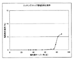
図7は、レジストベーク温度(ベーク時間10分)と犠牲層の断面のテーパー角の関係を示したものである。ポストベーク温度が高いほうが、テーパー角が小さくなることが判る。しかし、180度以上でベークするとレジストが変質してしまい、RIE後の剥離が困難になる場合がある。
FIG. 7 shows the relationship between the resist baking temperature (baking
犠牲層にテーパー角を付けたサンプルを、テトラ・メチル・アンモニウム・ハイドライド(TMAH)に浸せきして、裏面よりシリコンを異方性エッチングした。エッチング条件は、TMAH/H2O=21%、液温度83℃、エッチング時間は12時間であった。すると、図2のようにシリコンに開いた穴は最後には犠牲層に到達し、犠牲層をエッチングしてエッチングストップ層で止まる。 A sample with a tapered angle in the sacrificial layer was immersed in tetramethylammonium hydride (TMAH), and silicon was anisotropically etched from the back surface. Etching conditions were TMAH / H 2 O = 21%, liquid temperature 83 ° C., and etching time was 12 hours. Then, as shown in FIG. 2, the hole opened in the silicon finally reaches the sacrificial layer, and the sacrificial layer is etched to stop at the etching stop layer.
図8は、犠牲層のテーパー角と、エッチングストップ層の亀裂発生確率を示したものである。テーパー角が75度以下の時、亀裂の発生確率が急激に減少していることが判った。 FIG. 8 shows the taper angle of the sacrificial layer and the crack generation probability of the etching stop layer. It has been found that when the taper angle is 75 degrees or less, the probability of occurrence of cracks sharply decreases.
以上述べたように本発明によれば、エッチング犠牲層にテーパー角を付けることによって、異方性エッチングを使ったインク供給口形成時のエッチングストップ層の割れの確率が飛躍的に低下して歩留まりが向上し、低温で安価なプロセスを使って高品位な印字が可能なインクジェット記録ヘッドを提供することができる。 As described above, according to the present invention, by providing a taper angle to the etching sacrificial layer, the probability of cracking of the etching stop layer when forming the ink supply port using anisotropic etching is drastically reduced, and the yield is increased. And an inkjet recording head capable of high-quality printing using a low-temperature and inexpensive process can be provided.
次に、本発明の詳細を実施例の記述に従って説明する。 Next, details of the present invention will be described in accordance with the description of the embodiments.
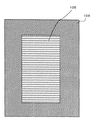
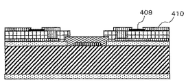
図9は本発明による実施態様例を示すインクジェット記録ヘッドの製造工程途中のヒーターボード基板の模式図である。基板としては(100)または(110)のSiウエハが用いられる。ウエハの表面にAlCu膜を3000Å堆積しパターニングして犠牲層303とした。犠牲層の平面形状は、Si(100)基板の場合は図3のように長方形で、Si(110)基板の場合は図10のように、狭角が70.5度の平行四辺形とする。また、犠牲層の側面にはテーパーが付けられていて、基板表面となす角度は、一般には75度以下、好ましくは70度以下、最適には60度以下である。
FIG. 9 is a schematic view of a heater board substrate in the course of the manufacturing process of the ink jet recording head showing an embodiment according to the present invention. As the substrate, a (100) or (110) Si wafer is used. A
その上にスパッター、蒸着やプラズマCVDによって薄膜を堆積してエッチングストップ層304とした。このエッチンッグストップ層の膜厚は、一般には1000〜20000Å、好ましくは2000〜16000Å、最適には3000〜13000Åである。
A thin film was deposited thereon by sputtering, vapor deposition, or plasma CVD to form an
犠牲層に隣接して、ヒーター305や配線306等が配置されている。
A
また基板の裏面には、耐アルカリ性の膜をパターニングしたエッチングパターン307が形成してあり、ここから異方性エッチングにより、表面の犠牲層へ向かって貫通口を開けインク供給口を形成する。
Further, an
次に、本発明によるインクジェット記録ノズルのプロセスを図11〜図25を使って順を追って説明する。 Next, the process of the ink jet recording nozzle according to the present invention will be described step by step with reference to FIGS.
(1)基板面方位(110)のシリコン基板401に、例えば熱酸化やCVD法などで絶縁膜402を形成し、フォトリソ技術によって図11(平面図 図10)のようにインク供給口を設けるための所望のパターン403を形成する。
(1) To form an
(2)AlやCu等の抵抗が低く、TMAH(テトラ・メチル・アンモニウム・ハイドライド)等の異方性エッチング用エッチャントに対するエッチング速度が大きな金属を堆積、パターニングして、下層配線404と犠牲層405を形成する。エッチング犠牲層は、裏面からエッチングが進行してエッチャントが犠牲層に到達するとSiウエハよりエッチングレートが格段に速いので短時間にエッチングされ、犠牲層パターンに対応した開口部を開けることができるものである。この時のパターンは基板に対して垂直にエッチング穴があくように、狭角が70.5度をなす平行四辺形とし、平行四辺形の長辺および短辺は(111)と等価の面に平行になるように配置する。
(2) A metal having a low resistance such as Al or Cu and a high etching rate for an etchant for anisotropic etching such as TMAH (tetra-methyl-ammonium hydride) is deposited and patterned to form the
犠牲層は、リアクティブ・イオン・エッチング(RIE)等によりパターニングされ、ポストベーク温度を変化させることによってテーパーをつけたレジストを用いて、断面形状がテーパー状になるようにエッチングした。レジストのポストベーク温度が高いほうが、テーパー角が小さくなることが判る。しかし、高温でベークするとレジストが変質してしまい、エッチング後の剥離が困難になる。犠牲層の側面にはテーパーが付けられていて、基板表面となす角度は、一般には75度以下、好ましくは70度以下、最適には60度以下である。 The sacrificial layer was patterned by reactive ion etching (RIE) or the like, and etched using a resist that was tapered by changing the post-bake temperature so that the cross-sectional shape was tapered. It can be seen that the taper angle becomes smaller as the resist post-bake temperature is higher. However, if the baking is performed at a high temperature, the resist changes in quality, and peeling after etching becomes difficult. The side surface of the sacrificial layer is tapered, and the angle formed with the substrate surface is generally 75 degrees or less, preferably 70 degrees or less, and optimally 60 degrees or less.
(3)基板表面上にエッチングストップ層406として、プラズマCVD法によって、SiNまたはSiON膜を堆積する。エッチングストップ層は、膜応力を調整するために2種以上の膜を積層しても良い。
(3) An SiN or SiON film is deposited as an
積層されたエッチングストップ膜のトータルの膜厚は、一般には2000Å〜2μm、好ましくは3000〜15000Å、最適には4000〜13000Åである。また積層されたエッチングストップ膜のトータルの応力は、一般には2×10exp−9dyne/cm2以下、より好ましくは1.8×10exp−9dyne/cm2以下、最適には1.5×10exp−9dyne/cm2以下である。
The total thickness of the laminated etching stop film is generally 2000-2 μm, preferably 3000-15000 mm, and most preferably 4000-13000 mm. The total stress of the laminated etching stop film is generally 2 × 10 exp-9 dyne /
(4)プラズマCVD等を使って、SiNやSiON、SiO2等の膜を堆積して層間絶縁膜407とする。さらに、層間絶縁膜にコンタクトホール408を形成する。
(4) A film such as SiN, SiON, or
(5)インク供給口に合わせて、インク吐出圧力発生素子としてヒーター部409形成する。ヒーター材料としては、Ta、TaN、TaNSi等などの金属膜をスパッターや真空蒸着等によって堆積しパターニングする。さらに電力供給用の上層電極410としてAl、Mo、Ni,Cu等の金属膜を同様にして形成する。
(5) A
(6)ヒーターには耐久性の向上を目的としてプラズマCVDでSiN膜411を堆積し保護膜とする。
(6) A
(7)この上に、耐キャビテーション膜412としてスパッター法等でTaを堆積しパターニングする。この膜の膜厚は、好ましくは1000〜5000Å、さらに好ましくは2000〜4000Å、最適には2500〜3500Åである。
(7) On this, Ta is deposited and patterned as a cavitation
また、配線とヒーターの形成の順番等に特に制限がないのは言うまでもない。 Needless to say, there is no particular limitation on the order of forming the wiring and the heater.
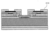
(8)樹脂製のノズルの密着性を上げるためと、裏面をアルカリ性エッチャントから保護するために、耐食性の高い樹脂膜413を形成する。そして、ヒーター部とインク供給口部をパターニングする。
(8) A
(9)インク流路確保のために、強アルカリや有機溶剤等で溶解可能な樹脂でパターン414を形成する。このパターンは、印刷法や感光性樹脂によるパターニング等で形成する。
(9) In order to secure the ink flow path, the
(10)インク流路のパターンの上に、被覆樹脂層415を形成する。この被覆樹脂層は微細パターンを形成するので感光性レジストが望ましく、さらに流路を形成した樹脂層を除去する際のアルカリや溶剤等によって変形変質しない性質が必要である。
(10) A
(11)次に流路の被覆樹脂層をパターニングして、ヒーター部409に対応したインク吐出口416と電極の外部接続部を形成する。この後、被覆樹脂層を光や熱等によって硬化する。
(11) Next, the coating resin layer of the flow path is patterned to form the
(12)この基板のノズル形成面側を保護するためレジストで保護膜417を形成する。
(12) A
(13)裏面のSiNまたはSiO2などをフォトリソ技術を使って、裏面のインク供給口のパターン部分418を除去しウエハ面を露出させる。このパターンの形状は、犠牲層とは鏡像関係になるように形成する。裏面のエッチングマスク膜の製法は、プラズマCVDに限定されるものではなく、LPCVD法や常圧CVD、熱酸化法などでも良い。
(13) Using a photolithographic technique, the back surface of the SiN or SiO2 is removed from the ink supply
(14)次に裏面の平行四辺形の狭角の近傍部分(裏面の平面図26)に、エッチング先導孔419をあける。一般的には、レーザー加工などが用いられるが、放電加工、ブラスト等でも良い。
(14) Next, an
この先導孔は、エッチングストップ層に限りなく近くまであける。先導孔の深さは、一般には基板厚さの60%以上、好ましくは70%以上、最適には80%以上である。また、基板を貫通してはならない。この先導孔によって、平行四辺形の狭角から発生する斜めの(111)面が抑制される。 This lead hole can be as close as possible to the etching stop layer. The depth of the leading hole is generally 60% or more of the substrate thickness, preferably 70% or more, and optimally 80% or more. Also, it must not penetrate the substrate. By this leading hole, the oblique (111) plane generated from the narrow angle of the parallelogram is suppressed.
(15)この基板をアルカリ系エッチャント(KOH、TMAH、ヒドラジン等)に浸け、(111)面が出るように異方性エッチングすると、平面形状が平行四辺形((100)基板の場合長方形)の貫通穴が形成される。 (15) When this substrate is immersed in an alkaline etchant (KOH, TMAH, hydrazine, etc.) and anisotropic etching is performed so that the (111) plane appears, the planar shape is a parallelogram (rectangular for (100) substrate). A through hole is formed.
(16)エッチングストップ層406のSiN等の膜をフッ酸等の薬液または、ドライエッチ等で部分的に除去してインク供給口を開口する。最後にインク流路形成材414を除去し、インクの流路420を確保する。
(16) The film of SiN or the like of the
上記プロセスにおいて、基板の加工手順は特に限定されるものではなく、任意に選ぶことができる。 In the above process, the substrate processing procedure is not particularly limited, and can be arbitrarily selected.
以下に、本発明によるインクジェット記録ヘッドの基板について説明する。 The substrate of the ink jet recording head according to the present invention will be described below.
図9は本発明による実施態様例を示すインクジェット記録ヘッドの製造工程途中のヒーターボード基板の模式図である。基板として5インチΦSi(110)ウエハを用いた。ウエハの表面にAlCu膜を3000Å堆積し平面図10のようにパターニングして犠牲層303とした。犠牲層の平面形状は、狭角が70.5度の平行四辺形とした。犠牲層の幅は160μm、長さは8mmとした。また、犠牲層の側面にはテーパーが付けられていて、基板表面となす角度は、45度とした。
FIG. 9 is a schematic view of a heater board substrate in the course of the manufacturing process of the ink jet recording head showing an embodiment according to the present invention. A 5-inch ΦSi (110) wafer was used as the substrate. A
その上にSiN膜を8000Å堆積してエッチングストップ層304とした。この時のSiN膜の成膜条件は、SiH4/NH3/N2=500/1500/6300sccm、圧力150mtorr、基板温度380℃、RF 1700Wであった。
An SiN film of 8000 mm was deposited thereon to form an
犠牲層に隣接して、TaSiNのヒーター305とAlCuの配線306を配置した。
A
また基板の裏面には、酸化膜5000Åの上に耐アルカリ性の膜(HIMAL日立化成製)310を犠牲層と鏡像になるようにパターニングしてエッチングパターン307を形成した。
On the back surface of the substrate, an
ここから異方性エッチングにより、表面の犠牲層へ向かって貫通口を開けインク供給口を形成する。 From here, through holes are opened toward the sacrificial layer on the surface by anisotropic etching to form ink supply ports.
以下に、本発明によるインクジェット記録ヘッドの基板の他の実施例について説明する。 Hereinafter, other embodiments of the substrate of the ink jet recording head according to the present invention will be described.
図27は本発明による実施態様例を示すインクジェット記録ヘッドの製造工程途中のヒーターボード基板の模式図である。基板として5インチΦSi(100)ウエハを用いた。ウエハの表面にAl膜を3000Å堆積し平面図3のようにパターニングして犠牲層とした。犠牲層の平面形状は、長方形とした。犠牲層の幅は100μm、長さは10mmとした。また、犠牲層の側面にはテーパーが付けられていて、基板表面となす角度は、65度とした。 FIG. 27 is a schematic view of a heater board substrate in the middle of the manufacturing process of the ink jet recording head showing an embodiment according to the present invention. A 5-inch ΦSi (100) wafer was used as the substrate. A 3000-thick Al film was deposited on the surface of the wafer and patterned as shown in plan view 3 to form a sacrificial layer. The planar shape of the sacrificial layer was a rectangle. The sacrificial layer had a width of 100 μm and a length of 10 mm. The side surface of the sacrificial layer is tapered, and the angle formed with the substrate surface is 65 degrees.
その上にSiN膜を6000Å堆積してエッチングストップ層503とした。
An SiN film of 6000 mm was deposited thereon to form an
犠牲層に隣接して、TaNのヒーター504とAlの配線505を配置した。
A
また基板の裏面には、プラズマSiN膜506を6000Å堆積し、その上に耐アルカリ性の膜(HIMAL日立化成製)507を平面図4のようにパターニングしたエッチングパターンが形成した。このパターンは、異方性エッチングによってウエハ断面にテーパーが付くことを考慮して、幅600μm、長さ11mmの長方形とした。
Further, on the back surface of the substrate, a
ここから異方性エッチングにより、表面の犠牲層へ向かって貫通口を開けインク供給口を形成する。 From here, through holes are opened toward the sacrificial layer on the surface by anisotropic etching to form ink supply ports.
本発明のインクジェット記録ヘッドの製造方法について、図28〜図41を使って順を追って説明する。 A method for manufacturing the ink jet recording head of the present invention will be described step by step with reference to FIGS.
図28のように、厚さ625μmで5インチΦの(100)面のSiウエハ601を熱酸化して、SiO2層602を14000Å形成した。次に、SiO2をパターニングして供給口開口部603を形成した。スパッターでAl膜を3000Å堆積した。フォトリソ技術によって図22のようにパターニングして犠牲層604と下層電極配線605を形成した。犠牲層の幅は120μm、長辺方向は15mmとした。
As shown in FIG. 28, a
この時、Al膜のパターニングは、レジスト(OFPR 東京応化製。OFPRは登録商標。)を3μm塗布し、露光・現像した後、150℃で10分間ポストベークしてレジストにテーパーを付けた。これを、RIEによって、テーパー状にエッチングした。条件は、BCl3/CF4/Cl2=75/20/50sccm、12mtorr、RF 1500Wであった。テーパー角度は60度であった。
At this time, patterning of the Al film was performed by applying a resist (OFPR, manufactured by Tokyo Ohka Kogyo, OFPR is a registered trademark) of 3 μm, exposing and developing, and then post-baking at 150 ° C. for 10 minutes to taper the resist. This was etched into a tapered shape by RIE. The conditions were BCl 3 / CF 4 /
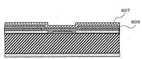
エッチングストップ層と層間絶縁膜を兼用した膜として、図30のようにプラズマCVDでSiON膜606を3000Å堆積した。さらに、プラズマCVDでSiN膜607を3000Å堆積した。
As a film that doubles as an etching stop layer and an interlayer insulating film, 3000 nm of
フォトリソ技術を使い、図31のように層間絶縁膜にコンタクトホール608を形成した。
Using a photolithography technique, a
さらに、スパッターにより、TaNを500ÅとAlを3000Å連続成膜しパターニングして、上層配線電極610とヒーター609を形成する。
Further, the
感光性樹脂としてポリメチルイソプロペニルケトン(東京応化ODUR−1010)を20μm塗布してパターニングして、図33のようにインク流路型材611を形成した。さらに図44に示した感光性樹脂層612を10μm塗布しパタ−ニングして、図35のようにインク吐出口613を形成した。なお、図44に記載のエピコートは登録商標である。
An ink
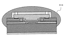
ノズル形成面側を保護するために、ゴム系レジスト(東京応化製 OBC)で保護膜614を形成した。ノズルの裏面側のSiO2をパターニングして、裏面インク供給口615を形成した。このパターンは、幅620μm長さ16mmの長方形とした。
In order to protect the nozzle forming surface side, a
この基板を20%のTMAH水溶液に浸漬して異方性エッチングした。エッチャント温度は83℃、エッチング時間は12時間とした。これは基板の厚み625μmをジャストエッチする時間に対して10%のオーバーエッチ時間とした。 This substrate was immersed in 20% TMAH aqueous solution and anisotropically etched. The etchant temperature was 83 ° C. and the etching time was 12 hours. This was an overetching time of 10% with respect to the time for just etching the thickness of the substrate of 625 μm.
エッチングは図38のようにAlの犠牲層まで進み、エッチングストップ層606の前で止まっている。この時、エッチングストップ層に亀裂はなく、流路形成樹脂層611やノズル部612へのエッチング液の浸入は見られなかった。
The etching proceeds to the Al sacrificial layer as shown in FIG. 38 and stops in front of the
次に、図39のようにエッチングストップ層のSiONとSiNをCDE法によって除去した。エッチング条件は、CF4/O2/N2=300/250/5sccm、RF800W、圧力250mtorrであった。
Next, as shown in FIG. 39, SiON and SiN in the etching stop layer were removed by the CDE method. Etching conditions were CF 4 /
図40のように、乳酸メチル中で超音波を掛け樹脂411を除去して、インク流路616を形成した。最後に、図41のようにメチルイソブチルケトンに浸漬後、キシレン中で超音波を掛け保護膜を除去してインクジェット記録ヘッドが完成した。
As shown in FIG. 40, ultrasonic waves were applied in methyl lactate to remove the
このインクジェット記録ヘッドを使って、吐出周波数15KHzで印字テストを行ったが、15mm幅全域にわたって、印字のカスレ、濃度ムラ、インクの不吐出のない高品位な印字物が得られた。 Using this ink jet recording head, a printing test was performed at an ejection frequency of 15 KHz. A high-quality printed matter free from printing blur, density unevenness, and non-ejection of ink was obtained over the entire 15 mm width.
(比較例1)
以下に、本発明の比較例を説明する。
(Comparative Example 1)
Below, the comparative example of this invention is demonstrated.
ヒーター、電極、ノズル等の構成や形成方法は実施例1と同じ構造で、犠牲層のパターニング時に、レジストのポストベーク温度を100℃にして、RIE後の犠牲層側面のテーパー角は85度であった。 The structure and formation method of the heater, electrodes, nozzles, etc. are the same as those in Example 1. At the time of patterning the sacrificial layer, the resist post-baking temperature is 100 ° C., and the taper angle on the side surface of the sacrificial layer after RIE is 85 degrees. there were.
これ以降の工程は全て、実施例1と同様にした。 All subsequent steps were the same as in Example 1.
このインクジェット記録ヘッドを使って、吐出周波数15KHzで印字テストを行ったが、インク吐出されない白抜けの部分があった。ヘッドを観察してみると、樹脂製のノズルの一部に、エッチングストップ層の亀裂が原因と思われるアルカリによる浸蝕の後が見つかった。 Using this ink jet recording head, a print test was performed at an ejection frequency of 15 KHz, but there were white spots where ink was not ejected. When the head was observed, a part of the resin nozzle was found after alkali erosion, which seems to be caused by cracks in the etching stop layer.
以下に、本発明によるインクジェット記録ヘッドの他の製造方法について、順を追って説明する。 Hereinafter, another method for manufacturing the ink jet recording head according to the present invention will be described in order.
図11のように、厚さ780μm、幅150mm長さ330mmの(110)面のSiウエハ401の上を熱酸化して、SiO2層402を8000Å形成した。次に、SiO2をパターニングして供給口開口部403を形成した。スパッターでAlCu膜を3000Å堆積した。この膜のCuの含有量は0.5%であった。フォトリソ技術によって図12のように(犠牲層の平面形状は図42のように平行四辺形にパターニングして)犠牲層405と下層電極配線404を形成した。犠牲層の幅は120μm、長辺方向は2mmで、隣接した犠牲層間のハリ420に相当する部分の幅は、60μmとした。犠牲層は、ハリを挟んで134本直列に並べた。
As shown in FIG. 11, the top surface of the (110)
この時、AlCu膜のパターニングは、レジスト(OFPR 東京応化製)を3μm塗布し、露光・現像した後、170℃で8分間ポストベークしてレジストにテーパーを付けた。これを、RIEによって、テーパー状にエッチングした。条件は、BCl3/Cl2=75/200sccm、20mtorr、RF 600Wであった。テーパー角度は45度であった。
At this time, patterning of the AlCu film was performed by applying a resist (OFPR Tokyo Ohka Kogyo Co., Ltd.) of 3 μm, exposing and developing, and post-baking at 170 ° C. for 8 minutes to taper the resist. This was etched into a tapered shape by RIE. The conditions were BCl 3 /
次に、エッチングストップ層として、プラズマCVDでSiN膜406を8000Å堆積した。
Next, 8000 mm of
この時の成膜条件は、SiH4/NH3/N2= 500/1500/6300sccm、圧力1500mtorr、基板温度400℃、RF1700Wであった。
The film formation conditions at this time were SiH 4 / NH 3 /
フォトリソ技術を使い、図13のように犠牲層405の周囲を覆うようにパターニングした後、層間絶縁膜407としてSiONを15000Å成膜した。この時の成膜パラメーターは、SiH4/N2O/N2= 250/1200/4000sccm、圧力1500mtorr、基板温度400℃、RF1700W、組成比Si/O/N=37/61/2であった。
After patterning so as to cover the periphery of the
この後は、図14のように層間絶縁膜にコンタクトホール408を形成し、TaSiN(組成比44/43/13)を500ÅとAlを3000Å連続成膜してパターニングして、図15のようにヒーター409と上部配線410を形成した。
Thereafter, contact holes 408 are formed in the interlayer insulating film as shown in FIG. 14, and 500 nm of TaSiN (composition ratio 44/43/13) and 3000 mm of Al are continuously formed and patterned, as shown in FIG. A
次にヒーター保護膜411として、プラズマCVDのSINを3000Å堆積、パターニングした。成膜条件は、SiH4/NH3/N2= 180/480/2000sccm、圧力1500mtorr、基板温度300℃、RF1700Wであった。
Next, 3000 nm of plasma CVD SIN was deposited and patterned as the heater
さらに、インクの発泡によるキャビテーションからヒーターを保護するため、Taを3000Åをスパッターで堆積パターニングして、耐キャビテーション膜412を形成した。
Further, in order to protect the heater from cavitation due to ink foaming, 3000 liters of Ta was deposited and patterned by sputtering to form a cavitation
樹脂製のノズルの密着性を上げるためと、裏面をアルカリエッチャントから保護するために、耐食性の高いポリエーテルアミド系樹脂膜(日立化成製 HIMAL)413を2μm塗布焼成して形成し、図18のようにヒーター部とインク供給口部をパターニングで露出させた。 In order to increase the adhesion of the resin nozzle and to protect the back surface from the alkali etchant, a polyetheramide-based resin film (HIMAL) 413 having high corrosion resistance is formed by applying and baking 2 μm. Thus, the heater part and the ink supply port part were exposed by patterning.
感光性樹脂としてポリメチルイソプロペニルケトン(東京応化ODUR−1010)を20μm塗布してパターニングして、図19のようにインク流路形成材414を形成した。さらに図44に示した感光性樹脂415を10μm塗布しパタ−ニングして、図20のようにインク吐出口416を形成した。
As a photosensitive resin, polymethyl isopropenyl ketone (Tokyo Ohka ODUR-1010) was applied by 20 μm and patterned to form an ink flow
ノズル形成面側を保護するために、ゴム系レジスト(東京応化製OBC)で保護膜417を形成した。ノズル形成された裏面のSiO2をパターンニングして、インク供給口418を形成した。この時のパターンは、図43のように表面の犠牲層とは鏡像関係になるような平行四辺形にした。そして、表面と同様にハリに相当する部分の幅を120μm設けた。
In order to protect the nozzle forming surface side, a
次に裏面のインク供給口パターン部の平行四辺形の窓の狭角に隣接した部分に、図43のようにYAGレーザーで非貫通のエッチング先導孔419を開けた。この時の穴の径は30〜35μm、深さは550〜730μmであった。
Next, a non-penetrating
この基板を21%のTMAH水溶液に浸漬して異方性エッチングした。エッチャント温度は83℃、エッチング時間は9時間とした。これは基板の厚み780μmをジャストエッチする時間に対して10%のオーバーエッチ時間とした。 This substrate was immersed in a 21% TMAH aqueous solution and anisotropically etched. The etchant temperature was 83 ° C. and the etching time was 9 hours. This was an overetching time of 10% with respect to the time for just etching the thickness of the substrate of 780 μm.
エッチングは図22のようにAlCuの犠牲層まで進み、エッチングストップ層406の前で止まっている。この時、エッチングストップ層に亀裂はなく、流路形成樹脂層414やノズル部415へのエッチング液の浸入は見られなかった。
The etching proceeds to the AlCu sacrificial layer as shown in FIG. 22 and stops in front of the
次に、図23のようにエッチングストップ層のSiONとSiNをCDE法によって除去した。エッチング条件は、CF4/O2/N2=300/250/5sccm、RF800W、圧力250mtorrであった。
Next, as shown in FIG. 23, SiON and SiN in the etching stop layer were removed by the CDE method. Etching conditions were CF 4 /
図24のようにメチルイソブチルケトンに浸漬後、キシレン中で超音波を掛け保護膜を除去して、乳酸メチル中で超音波を掛け樹脂414を除去して、インク流路420を形成しインクジェット記録ヘッドができた。
As shown in FIG. 24, after immersion in methyl isobutyl ketone, the protective film is removed by applying ultrasonic waves in xylene, and the
このインクジェット記録ヘッドを使って、吐出周波数10KHzで印字テストを行ったが、270mm幅全域にわたって、印字のカスレ、濃度ムラ、インクの不吐出のない高品位な印字物が得られた。 Using this ink jet recording head, a printing test was performed at an ejection frequency of 10 KHz. A high-quality printed matter free from printing blur, density unevenness, and non-ejection of ink was obtained over the entire width of 270 mm.
101 Si基板
102 犠牲層
103 エッチングストップ層
104 エッチングマスク材
105 インク供給口開口部
106 耐アルカリ性レジスト
201 Si基板
202 犠牲層
203 エッチングストップ層
204 インク流路形成型材
205 ノズル形成樹脂
301 シリコンウエハ基板
302 絶縁膜
303 犠牲層
304 エッチングストップ層
305 ヒーター
306 電極
307 インク供給口パターン
309 絶縁膜
310 耐アルカリ性樹脂膜
401 Si基板
402 SiO2
403 供給口開口部
404 下層配線電極
405 犠牲層
406 エッチングストップ層
407 層間絶縁膜
408 コンタクトホール
409 ヒーター
410 上層配線
411 保護膜
412 耐キャビテーション膜
413 密着性向上用樹脂膜
414 インク流路形成材
415 ノズル形成材
416 吐出口
417 エッチング用保護膜
418 裏面供給口
419 レーザー加工エッチング先導孔
420 インク流路
501 Si基板
502 犠牲層
503 エッチングストップ層
504 ヒーター
505 配線電極
506 エッチングマスク絶縁膜
507 耐アルカリ性樹脂膜
601 Si基板
602 絶縁膜
603 供給口開口部
604 犠牲層
605 下層配線電極
606 エッチングストップ層
607 層間絶縁膜
608 コンタクトホール
609 ヒーター
611 インク流路形成材
612 ノズル形成材
613 吐出口
614 エッチング用保護膜
615 裏面供給口
616 インク流路
DESCRIPTION OF
403
Claims (7)
Priority Applications (1)
| Application Number | Priority Date | Filing Date | Title |
|---|---|---|---|
| JP2006065966A JP2007237671A (en) | 2006-03-10 | 2006-03-10 | Method for manufacturing inkjet recording head |
Applications Claiming Priority (1)
| Application Number | Priority Date | Filing Date | Title |
|---|---|---|---|
| JP2006065966A JP2007237671A (en) | 2006-03-10 | 2006-03-10 | Method for manufacturing inkjet recording head |
Publications (1)
| Publication Number | Publication Date |
|---|---|
| JP2007237671A true JP2007237671A (en) | 2007-09-20 |
Family
ID=38583651
Family Applications (1)
| Application Number | Title | Priority Date | Filing Date |
|---|---|---|---|
| JP2006065966A Withdrawn JP2007237671A (en) | 2006-03-10 | 2006-03-10 | Method for manufacturing inkjet recording head |
Country Status (1)
| Country | Link |
|---|---|
| JP (1) | JP2007237671A (en) |
-
2006
- 2006-03-10 JP JP2006065966A patent/JP2007237671A/en not_active Withdrawn
Similar Documents
| Publication | Publication Date | Title |
|---|---|---|
| JPH10286960A (en) | Ink jet recording head and manufacture thereof | |
| EP1445102B1 (en) | Method for producing ink jet head | |
| KR20050000347A (en) | Method for manufacturing liquid ejection head | |
| JP4054583B2 (en) | Inkjet printhead manufacturing method | |
| US6818138B2 (en) | Slotted substrate and slotting process | |
| JP4979793B2 (en) | Manufacturing method of substrate for liquid discharge head | |
| JP4480132B2 (en) | Manufacturing method of liquid discharge head | |
| JP3937804B2 (en) | Method for manufacturing structure having through hole | |
| US8647896B2 (en) | Process for producing a substrate for a liquid ejection head | |
| US7634855B2 (en) | Method for producing ink jet recording head | |
| JP2006224596A (en) | Inkjet recording head and method for manufacturing inkjet recording head | |
| JP5038054B2 (en) | Liquid discharge head and manufacturing method thereof | |
| JP2007245639A (en) | Manufacturing method of inkjet recording head | |
| JP4693496B2 (en) | Liquid discharge head and manufacturing method thereof | |
| JP2007245638A (en) | Manufacturing method of inkjet recording head | |
| JP2006224590A (en) | Method for manufacturing inkjet recording head | |
| JP2007237671A (en) | Method for manufacturing inkjet recording head | |
| JP2008120003A (en) | Inkjet recording head and manufacturing method for substrate for the head | |
| JP2007253472A (en) | Inkjet recording head and method for manufacturing inkjet recording head | |
| JP2003136491A (en) | Structure with through-hole, method for manufacturing the same, and liquid discharging head | |
| JP2009148941A (en) | Inkjet recording head and method for production of the same | |
| JP2006224593A (en) | Method for manufacturing inkjet recording head | |
| JP2007283667A (en) | Inkjet recording head and manufacturing method for inkjet recording head | |
| JP2006224591A (en) | Method for manufacturing inkjet recording head | |
| JP2006225745A (en) | Structure of thin film element and method for producing the same |
Legal Events
| Date | Code | Title | Description |
|---|---|---|---|
| A300 | Withdrawal of application because of no request for examination |
Free format text: JAPANESE INTERMEDIATE CODE: A300 Effective date: 20090512 |