JP2007235068A - Wafer machining method - Google Patents
Wafer machining method Download PDFInfo
- Publication number
- JP2007235068A JP2007235068A JP2006058330A JP2006058330A JP2007235068A JP 2007235068 A JP2007235068 A JP 2007235068A JP 2006058330 A JP2006058330 A JP 2006058330A JP 2006058330 A JP2006058330 A JP 2006058330A JP 2007235068 A JP2007235068 A JP 2007235068A
- Authority
- JP
- Japan
- Prior art keywords
- wafer
- machining
- tape
- thickness
- dicing
- Prior art date
- Legal status (The legal status is an assumption and is not a legal conclusion. Google has not performed a legal analysis and makes no representation as to the accuracy of the status listed.)
- Pending
Links
Images


Classifications
-
- H—ELECTRICITY
- H01—ELECTRIC ELEMENTS
- H01L—SEMICONDUCTOR DEVICES NOT COVERED BY CLASS H10
- H01L21/00—Processes or apparatus adapted for the manufacture or treatment of semiconductor or solid state devices or of parts thereof
- H01L21/67—Apparatus specially adapted for handling semiconductor or electric solid state devices during manufacture or treatment thereof; Apparatus specially adapted for handling wafers during manufacture or treatment of semiconductor or electric solid state devices or components ; Apparatus not specifically provided for elsewhere
- H01L21/67005—Apparatus not specifically provided for elsewhere
- H01L21/67011—Apparatus for manufacture or treatment
- H01L21/67155—Apparatus for manufacturing or treating in a plurality of work-stations
- H01L21/67207—Apparatus for manufacturing or treating in a plurality of work-stations comprising a chamber adapted to a particular process
- H01L21/67219—Apparatus for manufacturing or treating in a plurality of work-stations comprising a chamber adapted to a particular process comprising at least one polishing chamber
-
- H—ELECTRICITY
- H01—ELECTRIC ELEMENTS
- H01L—SEMICONDUCTOR DEVICES NOT COVERED BY CLASS H10
- H01L21/00—Processes or apparatus adapted for the manufacture or treatment of semiconductor or solid state devices or of parts thereof
- H01L21/02—Manufacture or treatment of semiconductor devices or of parts thereof
- H01L21/04—Manufacture or treatment of semiconductor devices or of parts thereof the devices having at least one potential-jump barrier or surface barrier, e.g. PN junction, depletion layer or carrier concentration layer
- H01L21/18—Manufacture or treatment of semiconductor devices or of parts thereof the devices having at least one potential-jump barrier or surface barrier, e.g. PN junction, depletion layer or carrier concentration layer the devices having semiconductor bodies comprising elements of Group IV of the Periodic System or AIIIBV compounds with or without impurities, e.g. doping materials
- H01L21/30—Treatment of semiconductor bodies using processes or apparatus not provided for in groups H01L21/20 - H01L21/26
-
- B—PERFORMING OPERATIONS; TRANSPORTING
- B23—MACHINE TOOLS; METAL-WORKING NOT OTHERWISE PROVIDED FOR
- B23K—SOLDERING OR UNSOLDERING; WELDING; CLADDING OR PLATING BY SOLDERING OR WELDING; CUTTING BY APPLYING HEAT LOCALLY, e.g. FLAME CUTTING; WORKING BY LASER BEAM
- B23K26/00—Working by laser beam, e.g. welding, cutting or boring
- B23K26/36—Removing material
- B23K26/40—Removing material taking account of the properties of the material involved
-
- B—PERFORMING OPERATIONS; TRANSPORTING
- B23—MACHINE TOOLS; METAL-WORKING NOT OTHERWISE PROVIDED FOR
- B23K—SOLDERING OR UNSOLDERING; WELDING; CLADDING OR PLATING BY SOLDERING OR WELDING; CUTTING BY APPLYING HEAT LOCALLY, e.g. FLAME CUTTING; WORKING BY LASER BEAM
- B23K26/00—Working by laser beam, e.g. welding, cutting or boring
- B23K26/50—Working by transmitting the laser beam through or within the workpiece
- B23K26/53—Working by transmitting the laser beam through or within the workpiece for modifying or reforming the material inside the workpiece, e.g. for producing break initiation cracks
-
- H—ELECTRICITY
- H01—ELECTRIC ELEMENTS
- H01L—SEMICONDUCTOR DEVICES NOT COVERED BY CLASS H10
- H01L21/00—Processes or apparatus adapted for the manufacture or treatment of semiconductor or solid state devices or of parts thereof
- H01L21/02—Manufacture or treatment of semiconductor devices or of parts thereof
- H01L21/04—Manufacture or treatment of semiconductor devices or of parts thereof the devices having at least one potential-jump barrier or surface barrier, e.g. PN junction, depletion layer or carrier concentration layer
- H01L21/18—Manufacture or treatment of semiconductor devices or of parts thereof the devices having at least one potential-jump barrier or surface barrier, e.g. PN junction, depletion layer or carrier concentration layer the devices having semiconductor bodies comprising elements of Group IV of the Periodic System or AIIIBV compounds with or without impurities, e.g. doping materials
- H01L21/30—Treatment of semiconductor bodies using processes or apparatus not provided for in groups H01L21/20 - H01L21/26
- H01L21/302—Treatment of semiconductor bodies using processes or apparatus not provided for in groups H01L21/20 - H01L21/26 to change their surface-physical characteristics or shape, e.g. etching, polishing, cutting
- H01L21/304—Mechanical treatment, e.g. grinding, polishing, cutting
-
- H—ELECTRICITY
- H01—ELECTRIC ELEMENTS
- H01L—SEMICONDUCTOR DEVICES NOT COVERED BY CLASS H10
- H01L21/00—Processes or apparatus adapted for the manufacture or treatment of semiconductor or solid state devices or of parts thereof
- H01L21/67—Apparatus specially adapted for handling semiconductor or electric solid state devices during manufacture or treatment thereof; Apparatus specially adapted for handling wafers during manufacture or treatment of semiconductor or electric solid state devices or components ; Apparatus not specifically provided for elsewhere
- H01L21/67005—Apparatus not specifically provided for elsewhere
- H01L21/67011—Apparatus for manufacture or treatment
- H01L21/67092—Apparatus for mechanical treatment
-
- H—ELECTRICITY
- H01—ELECTRIC ELEMENTS
- H01L—SEMICONDUCTOR DEVICES NOT COVERED BY CLASS H10
- H01L21/00—Processes or apparatus adapted for the manufacture or treatment of semiconductor or solid state devices or of parts thereof
- H01L21/67—Apparatus specially adapted for handling semiconductor or electric solid state devices during manufacture or treatment thereof; Apparatus specially adapted for handling wafers during manufacture or treatment of semiconductor or electric solid state devices or components ; Apparatus not specifically provided for elsewhere
- H01L21/67005—Apparatus not specifically provided for elsewhere
- H01L21/67011—Apparatus for manufacture or treatment
- H01L21/67132—Apparatus for placing on an insulating substrate, e.g. tape
-
- H—ELECTRICITY
- H01—ELECTRIC ELEMENTS
- H01L—SEMICONDUCTOR DEVICES NOT COVERED BY CLASS H10
- H01L21/00—Processes or apparatus adapted for the manufacture or treatment of semiconductor or solid state devices or of parts thereof
- H01L21/70—Manufacture or treatment of devices consisting of a plurality of solid state components formed in or on a common substrate or of parts thereof; Manufacture of integrated circuit devices or of parts thereof
- H01L21/77—Manufacture or treatment of devices consisting of a plurality of solid state components or integrated circuits formed in, or on, a common substrate
- H01L21/78—Manufacture or treatment of devices consisting of a plurality of solid state components or integrated circuits formed in, or on, a common substrate with subsequent division of the substrate into plural individual devices
-
- B—PERFORMING OPERATIONS; TRANSPORTING
- B23—MACHINE TOOLS; METAL-WORKING NOT OTHERWISE PROVIDED FOR
- B23K—SOLDERING OR UNSOLDERING; WELDING; CLADDING OR PLATING BY SOLDERING OR WELDING; CUTTING BY APPLYING HEAT LOCALLY, e.g. FLAME CUTTING; WORKING BY LASER BEAM
- B23K2101/00—Articles made by soldering, welding or cutting
- B23K2101/36—Electric or electronic devices
- B23K2101/40—Semiconductor devices
-
- B—PERFORMING OPERATIONS; TRANSPORTING
- B23—MACHINE TOOLS; METAL-WORKING NOT OTHERWISE PROVIDED FOR
- B23K—SOLDERING OR UNSOLDERING; WELDING; CLADDING OR PLATING BY SOLDERING OR WELDING; CUTTING BY APPLYING HEAT LOCALLY, e.g. FLAME CUTTING; WORKING BY LASER BEAM
- B23K2103/00—Materials to be soldered, welded or cut
- B23K2103/50—Inorganic material, e.g. metals, not provided for in B23K2103/02 – B23K2103/26
Landscapes
- Engineering & Computer Science (AREA)
- Physics & Mathematics (AREA)
- Condensed Matter Physics & Semiconductors (AREA)
- General Physics & Mathematics (AREA)
- Manufacturing & Machinery (AREA)
- Computer Hardware Design (AREA)
- Microelectronics & Electronic Packaging (AREA)
- Power Engineering (AREA)
- Optics & Photonics (AREA)
- Plasma & Fusion (AREA)
- Mechanical Engineering (AREA)
- Chemical Kinetics & Catalysis (AREA)
- General Chemical & Material Sciences (AREA)
- Oil, Petroleum & Natural Gas (AREA)
- Chemical & Material Sciences (AREA)
- Dicing (AREA)
- Mechanical Treatment Of Semiconductor (AREA)
- Container, Conveyance, Adherence, Positioning, Of Wafer (AREA)
Abstract
Description
本発明は、ウェーハ加工方法に係り、特に、半導体ウェーハの平面加工からチップサイズに切断されたウェーハのマウントまでを欠陥なく行うのに好適なウェーハ加工方法に関する。 The present invention relates to a wafer processing method, and more particularly, to a wafer processing method suitable for performing from planar processing of a semiconductor wafer to mounting of a wafer cut to a chip size without defects.
半導体装置や電子部品等の製造工程では、先ず表面に半導体装置や電子部品等が形成されたウェーハに対して、プロービング、ダイシング、ダイボンディング、及びワイヤボンディング等の各工程を経た後、樹脂モールドされて半導体装置や電子部品等の完成品となるのが一般的である。 In the manufacturing process of semiconductor devices, electronic components, etc., the wafers with semiconductor devices, electronic components, etc. formed on the surface are first subjected to resin molding after going through various steps such as probing, dicing, die bonding, and wire bonding. In general, it is a finished product such as a semiconductor device or an electronic component.
ところで近年、メモリーカードや薄型ICカード等に組込まれる極薄の半導体装置や電子部品の需要が高まっており、厚さが100μm以下の極薄ウェーハの要求が増大している。このため、従来ではプロービング工程の後に、ダイシング工程によってウェーハを個々のチップに分割していたが、これに代えて、ダイシング工程の前にウェーハの裏面を研削(バックグラインド)し、100μm以下の極薄ウェーハとしてからダイシングを行うようになってきた。 In recent years, demand for ultra-thin semiconductor devices and electronic components incorporated in memory cards, thin IC cards, and the like has increased, and the demand for ultra-thin wafers with a thickness of 100 μm or less has increased. For this reason, conventionally, after the probing process, the wafer was divided into individual chips by the dicing process. Instead, the back surface of the wafer was ground (back grind) before the dicing process, and the poles were 100 μm or less. Dicing has been started after thin wafers.
このような背景の下に、従来の半導体装置や電子部品等のチップ製造方法では、図15のフロー図に示されるように、以下のような手順でチップの製造が行われる。 Against this background, in the conventional chip manufacturing method for semiconductor devices and electronic components, as shown in the flowchart of FIG. 15, the chip is manufactured in the following procedure.
先ず、表面に半導体装置や電子部品等が多数形成されたウェーハの表面を保護するため、片面に粘着剤を有する保護シート(保護テープとも称される)がウェーハ表面に貼られる(ステップS101)。次に、ウェーハを裏面から研削して所定の厚さに加工する裏面研削工程が行われる(ステップS103)。 First, in order to protect the surface of a wafer on which a large number of semiconductor devices, electronic components, and the like are formed on the surface, a protective sheet (also referred to as a protective tape) having an adhesive on one side is attached to the wafer surface (step S101). Next, a back surface grinding process is performed in which the wafer is ground from the back surface and processed to a predetermined thickness (step S103).
裏面研削工程の後、片面に粘着剤を有するダイシングシート(ダイシングテープとも称される)を用いてウェーハをダイシング用フレームに取付けるフレームマウント工程が行われ、ウェーハとダイシング用のフレームとが一体化される(ステップS105)。この状態でウェーハをダイシングシート側で吸着し、表面に貼付されている保護シートが剥離される(ステップS107)。 After the back grinding process, a frame mounting process is performed in which a wafer is mounted on a dicing frame using a dicing sheet (also referred to as dicing tape) having an adhesive on one side, and the wafer and the dicing frame are integrated. (Step S105). In this state, the wafer is adsorbed on the dicing sheet side, and the protective sheet attached to the surface is peeled off (step S107).
保護シートが剥離されたウェーハは、フレームごとダイシングソーに搬送され、高速回転するダイヤモンドブレードで個々のチップに切断される(ステップS109)。切断された個々のチップは、図16に示されるように、ダイシングシートSに貼付されたままバラバラにならず、ウェーハ状態を保っているので、ここでは、便宜上このウェーハ状態を保ったチップTの集合体をもウェーハWと呼ぶことにする。 The wafer from which the protective sheet has been peeled is transferred to the dicing saw together with the frame, and is cut into individual chips with a diamond blade that rotates at high speed (step S109). As shown in FIG. 16, the cut individual chips remain affixed to the dicing sheet S and remain in the wafer state, so here, for convenience, the chips T that have maintained the wafer state are maintained. The aggregate is also called a wafer W.
切断されたウェーハWは、エキスパンド工程において、ダイシングシートSが放射状に引き伸ばされて、個々のチップTの間隔が広げられ(ステップS111)、チップマウント工程において、リードフレーム等のパッケージ基材にマウントされる(ステップS113)。以上のような工程によりチップの製造が行われる。 In the expanding process, the cut wafer W is radially expanded with the dicing sheet S to widen the intervals between the individual chips T (step S111), and is mounted on a package substrate such as a lead frame in the chip mounting process. (Step S113). Chips are manufactured through the above-described steps.
ところが、従来のチップ製造方法では、厚さが100μm以下の極薄のウェーハWをダイシングソーにより切断した際、切断時にウェーハWにチッピングや割れが生じ、多くの不良チップが発生する問題があった。 However, in the conventional chip manufacturing method, when an extremely thin wafer W having a thickness of 100 μm or less is cut by a dicing saw, there is a problem that chipping or cracking occurs in the wafer W at the time of cutting and many defective chips are generated. .
この問題を解決する手段として、従来のダイシングソーによる切断に代えて、ウェーハWの内部に集光点を合わせたレーザー光を入射させ、ウェーハ内部に多光子吸収による改質領域を形成して個々のチップTに分割するレーザー加工方法に関する技術が提案されている(たとえば、特許文献1〜6参照。)。 As a means to solve this problem, instead of cutting with a conventional dicing saw, a laser beam with a focused point is made incident inside the wafer W, and a modified region by multiphoton absorption is formed inside the wafer to individually A technique relating to a laser processing method for dividing the chip T is proposed (for example, see Patent Documents 1 to 6).
上記の特許文献1〜6で提案されている技術は、従来のダイシングソーによるダイシング装置に代えて、図17に示されるように、レーザー光源LSから出射されたレーザー光LをウェーハWの内部に集光させ、ウェーハWの内部に連続して改質領域Kを形成することによりウェーハWを割断するダイシング装置(以下、レーザーダイシング装置と称する)を提案したものである。 The techniques proposed in the above-mentioned patent documents 1 to 6 replace the dicing apparatus using the conventional dicing saw with the laser light L emitted from the laser light source LS inside the wafer W as shown in FIG. The present invention proposes a dicing apparatus (hereinafter referred to as a laser dicing apparatus) that cleaves the wafer W by condensing and continuously forming the modified region K inside the wafer W.
レーザーダイシング装置では、高速回転するダイヤモンドブレードに代えて、レーザー光によりウェーハがチップに分割されるため、ウェーハに大きな力がかからず、チッピングや割れが発生しない。また、ウェーハに直接接触する部分がなく、熱や切削屑が発生しないため、切削水を必要としない。更に、内部に改質領域を形成してウェーハの割段を行いチップに分割するため、チップの間隔がダイヤモンドブレードによる切断よりも非常に狭く、一枚のウェーハからより多くのチップを得られる。
しかしながら、レーザーダイシング装置では、ダイシング後に各工程に使用される装置間を搬送される際、衝撃や振動により内部の改質領域を起点として割段されてしまう場合がある。そして、一旦割段された場合、ウェーハとしてのハンドリングができず、以降の工程の進行が大幅に妨げられるという問題があった。 However, in the laser dicing apparatus, when being transported between apparatuses used for each process after dicing, there are cases where the internal reforming region is divided as a starting point due to impact or vibration. And once divided, there is a problem that handling as a wafer cannot be performed, and the progress of the subsequent steps is greatly hindered.
本発明は、このような問題に対してなされたものであり、レーザーダイシング装置によりダイシングされたウェーハを、割段されずに後工程に供給(搬送)できるウェーハ加工方法を提供することを目的とする。 The present invention has been made for such a problem, and an object thereof is to provide a wafer processing method capable of supplying (carrying) a wafer diced by a laser dicing apparatus to a subsequent process without being divided. To do.
本発明は、前記目的を達成するために、ウェーハの裏面を研削加工し、研削後の前記ウェーハの裏面を研磨加工し、ウェーハの最終加工厚さT1より50〜500μm厚い厚さT2まで前記ウェーハの裏面を加工する第1の機械加工ステップと、第1の機械加工後の前記ウェーハにレーザー光を照射して内部へ改質領域を形成する改質領域形成ステップと、改質領域形成後の前記ウェーハの裏面を研削加工し、研削後の前記ウェーハの裏面を研磨加工し、ウェーハの最終加工厚さT1まで前記ウェーハの裏面を加工する第2の機械加工ステップと、を備えることを特徴とするウェーハ加工方法を提供する。 In order to achieve the above object, the present invention grinds the back surface of the wafer, polishes the back surface of the wafer after grinding, and forms the wafer to a thickness T2 that is 50 to 500 μm thicker than the final processing thickness T1 of the wafer. A first machining step for machining the back surface of the wafer, a modified region forming step for irradiating the wafer after the first machining with a laser beam to form a modified region therein, and after the modified region is formed And a second machining step for grinding the back surface of the wafer, polishing the back surface of the wafer after grinding, and processing the back surface of the wafer to a final processing thickness T1 of the wafer. A wafer processing method is provided.
本発明によれば、第1の機械加工ステップにおいて、ウェーハの最終加工厚さT1より50〜500μm厚い厚さT2までウェーハの裏面を加工する。すなわち、ダイシング後のウェーハの機械的強度が大幅に向上する。したがって、ダイシング後に各工程に使用される装置間を搬送される際、多少の衝撃や振動を受けても、内部の改質領域を起点として割段されてしまうような不具合は激減又は皆無となる。 According to the present invention, in the first machining step, the back surface of the wafer is processed to a thickness T2 that is 50 to 500 μm thicker than the final processing thickness T1 of the wafer. That is, the mechanical strength of the wafer after dicing is greatly improved. Therefore, when transported between devices used for each process after dicing, even if it receives a slight impact or vibration, the problem of being divided from the internal reforming region as a starting point is drastically reduced or eliminated. .
このように、本発明によれば、レーザーダイシング装置によりダイシングされたウェーハを、ダメージを与えることなくチップに分割することができる。 As described above, according to the present invention, the wafer diced by the laser dicing apparatus can be divided into chips without causing damage.
なお、厚さT2は、最終加工厚さT1より100〜300μm厚いことが好ましく、最終加工厚さT1より150〜250μm厚いことがより好ましい。 The thickness T2 is preferably 100 to 300 μm thicker than the final processed thickness T1, and more preferably 150 to 250 μm thicker than the final processed thickness T1.
本発明において、第1の機械加工前の前記ウェーハの表面に該ウェーハの表面に形成されたパターンを保護する保護用テープを貼着するテープ貼着ステップと、第2の機械加工後の前記ウェーハの表面に紫外線光を照射する紫外線光照射ステップと、紫外線光照射後の前記ウェーハの裏面にダイシングテープを貼着して前記ウェーハをフレームへマウントするテープマウントステップと、フレームへマウントされた前記ウェーハの表面に貼着されている前記保護用テープの剥離を行うテープ剥離ステップと、前記保護用テープが剥離された前記ウェーハの前記ダイシングテープが貼着された側より、前記ダイシングテープのエキスパンドを行い、前記ウェーハの各チップ間の間隔を拡張するエキスパンドステップと、を備えることが好ましい。 In the present invention, a tape adhering step for adhering a protective tape for protecting a pattern formed on the surface of the wafer to the surface of the wafer before the first machining, and the wafer after the second machining An ultraviolet light irradiation step for irradiating the surface of the wafer with ultraviolet light, a tape mounting step for attaching the dicing tape to the back surface of the wafer after the ultraviolet light irradiation and mounting the wafer on a frame, and the wafer mounted on the frame A tape peeling step for peeling off the protective tape attached to the surface of the wafer, and expanding the dicing tape from the side where the dicing tape is attached to the wafer from which the protective tape is peeled off. And an expanding step for expanding the interval between each chip of the wafer.
このように、ウェーハは、装置内の少ない移動距離で、裏面の研削加工から始まって、UV光照射、フレームへのマウント、保護シート剥離、及びエキスパンドまでの各ステップ(工程)を終了することが可能となる。したがって、搬送中や各工程の作業中にチップへダメージを与える可能性が最小限に抑えられる。また、エキスパンドされた状態でカセットへ格納されるため、チップマウント工程を直ちに進められるのでスループットの向上が可能となる。 In this way, the wafer can be completed within each step (process) from the grinding of the back surface to the UV light irradiation, mounting to the frame, peeling of the protective sheet, and expanding with a small movement distance in the apparatus. It becomes possible. Therefore, the possibility of damaging the chip during conveyance or during each process is minimized. Further, since it is stored in the cassette in an expanded state, the chip mounting process can be immediately advanced, so that the throughput can be improved.
また、本発明において、前記ウェーハの内部に形成する改質領域がウェーハの表面より厚さ方向にT1までの距離の位置であることが好ましい。このような厚さ方向に改質領域が形成されれば、ウェーハの割断が容易となる。 In the present invention, the modified region formed inside the wafer is preferably located at a distance from the surface of the wafer to T1 in the thickness direction. If the modified region is formed in such a thickness direction, the wafer is easily cleaved.
また、本発明において、第2の機械加工後の前記ウェーハをプラズマ洗浄するプラズマ洗浄ステップを備えることが好ましい。このような洗浄ステップを備えていれば、ウェーハの品質が向上する。 In the present invention, it is preferable that a plasma cleaning step of plasma cleaning the wafer after the second machining is provided. If such a cleaning step is provided, the quality of the wafer is improved.
以上説明したように、本発明によれば、レーザーダイシング装置によりダイシングされたウェーハを、ダメージを与えることなくチップに分割することができる。 As described above, according to the present invention, a wafer diced by a laser dicing apparatus can be divided into chips without causing damage.
以下、添付図面に従って、本発明に係るウェーハ加工方法の好ましい実施の形態について詳説する。 Hereinafter, preferred embodiments of a wafer processing method according to the present invention will be described in detail with reference to the accompanying drawings.
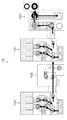
図1は、本発明が適用されるウェーハ加工装置10の全体構成を示す平面図である。このウェーハ加工装置10は、上流側(左側)より、平面加工装置10A、レーザーダイシング装置10B、平面加工装置10C、及びウェーハマウント装置10Dで構成されている。以下、順に説明する。
FIG. 1 is a plan view showing the overall configuration of a
平面加工装置10Aは、第1の機械加工ステップに使用され、平面加工装置10Cは、第2の機械加工ステップに使用される。
The
なお、平面加工装置を図1のように2台設けず、1台の平面加工装置10A(又は10C)で第1及び第2の機械加工ステップに対応させてもよい。
In addition, two plane processing apparatuses may not be provided as shown in FIG. 1, and one
図2は、平面加工装置10A(10C)の斜視図であり、図3は平面図である。図2に示されるように平面加工装置10A(10C)の本体112には、カセット収納ステージ114、アライメントステージ116、粗研削ステージ118、精研削ステージ120、研磨ステージ122、研磨布洗浄ステージ123、研磨布ドレッシングステージ127、及びウェーハ洗浄ステージ124が設けられている。
FIG. 2 is a perspective view of the
また、粗研削ステージ118、精研削ステージ120、研磨ステージ122は、図3の二点鎖線で示される仕切板125によって仕切られ、各々のステージ118、120、122で使用する加工液が隣接するステージに飛散するのが防止されている。
Further, the
仕切板125は図5、図6に示されるようにインデックステーブル134に固定されるとともに、インデックステーブル134に設置された4台のチャック(保持手段に相当)132、136、138、140を仕切るように十字形状に形成されている。また、研磨ステージ122は、他のステージから隔離するために、天板200を有するケーシング202によって覆われている。
As shown in FIGS. 5 and 6, the
このケーシング202の、仕切板125が通過する側面には、図7の如くブラシ204が取り付けられており、このブラシ204は、チャック140が加工位置に位置した時に、仕切板125の上面125A及び側面125Bに接触される。
A
これにより、チャック140が加工位置に位置すると、ケーシング202、仕切板125、及びブラシ204によって研磨ステージ122が略気密状態に保持されるので、精研削ステージ120で使用される研削加工液や加工屑が研磨ステージ122に浸入するのを防止でき、また、研磨ステージ122で使用される研磨加工液が研磨ステージ122から飛散するのを防止できる。
As a result, when the
したがって、双方の加工液が混入することに起因する加工不具合を防止できる。本例の研磨ステージ122は、化学機械研磨を行うもので、研磨加工液に化学研磨剤が含有されているので、このような研磨加工液に研削加工液が混入すると、化学研磨剤の濃度が低下し、加工時間が長くなるという不具合が生じる。よって、仕切板125を設けることによって、前記不具合を解消できる。
Therefore, it is possible to prevent a processing failure caused by mixing of both processing liquids. The polishing
なお、粗研削ステージ118は、図5、図6の如く本体112の側面、天板206、及び仕切板125によって囲まれており、また、精研削ステージ120も同様に本体112の側面、天板208、及び仕切板125によって囲まれている。これらの天板200、206、208には、各ステージのヘッドが挿通される貫通孔201、207、209が形成されている。
The rough
図6の符号210は、粗研削ステージ118を外部から隔離するためのブラシであり、このブラシ210は仕切板125の上面及び側面に接触されている。
A
図2、図3に示されるカセット収納ステージ114には、2台のカセット126、126が着脱自在にセットされ、これらのカセット126、126には裏面研削前のウェーハWが多数枚収納されている。このウェーハWは、搬送用ロボット130のハンド131によって1枚ずつ保持されて、次工程のアライメントステージ116に順次搬送される。
2 and 3, two
搬送用ロボット130は、本体112に立設された図示しないビームに昇降装置を介して吊り下げ支持してもよく、また、本体112の上面112Aに設置してもよい。搬送用ロボット130を吊り下げ支持すると、カセット収納ステージ114とアライメントステージ116との間隔を狭くすることができるので、平面加工装置10A(10C)の小型化を図ることができる。ロボット130は、汎用の6軸関節ロボットであり、その構成は周知であるので、ここではその説明を省略する。
The
アライメントステージ116は、カセット126から搬送されたウェーハWを所定の位置に位置合わせするステージである。このアライメントステージ116で位置合わせされたウェーハWは、搬送用ロボット130のハンド131に再度吸着保持された後、空のチャック132に向けて搬送され、このチャック132の吸着面に吸着保持される。
The
チャック132は、インデックステーブル134に設置され、また、同機能を備えたチャック136、138、140が、インデックステーブル134の図3の破線で示される回転軸135を中心とする円周上に90度の間隔をもって設置されている。
The
また、回転軸135には、図3に破線で示されるモータ(移動手段に相当)137のスピンドル(不図示)が連結されている。チャック136は、粗研削ステージ118に位置されており、吸着したウェーハWがここで粗研削される。
Further, a spindle (not shown) of a motor 137 (corresponding to moving means) indicated by a broken line in FIG. The
また、チャック138は、精研削ステージ120に位置され、吸着したウェーハWがここで仕上げ研削(精研削、スパークアウト)される。更に、チャック140は、研磨ステージ122に位置され、吸着したウェーハWがここで研磨され、研削で生じた加工変質層、及びウェーハWの厚さのバラツキ分が除去される。
Further, the
チャック132、136、138、140は、図4の如くその下面にスピンドル194と回転用モータ192が各々連結され、これらのモータ192の駆動力によって回転される。モータ192は、支持部材193を介してインデックステーブル134に支持されている。
As shown in FIG. 4, the
したがって、本実施の形態の平面加工装置10A(10C)は、モータ192とスピンドル194がチャック132、136、138、140に連結された状態で、チャック132、136、138、140がモータ137によって移動される装置である。
Therefore, in the
これにより、チャック132、136、138、140をモータ137で移動させる毎に、スピンドル194をチャック132、136、138、140から切り離したり、次の移動位置に設置されたスピンドル194にチャック132、136、138、140を連結したりする手間を省くことができる。
Thus, every time the
本実施の形態のチャック132、136、138、140は、その吸着面がセラミックス等の焼結体からなるポーラス材で形成されている。これによってウェーハWがポーラス材の表面にしっかりと吸着保持される。
The
図3に示されるウェーハWのチャック位置に位置されているチャック132は、ウェーハWが搬送されてくるまえに、その吸着面がクリーナ装置142(図3参照)によって洗浄される。クリーナ装置142は、レール144にスライド移動自在に設けられ、吸着面を洗浄する際に、レール144に沿って移動されチャック132上に位置される。
The
クリーナ装置142は除去部材143を有し、この除去部材143がチャック132の吸着面に当接されて吸着面に付着したスラッジ等のゴミを除去する。除去部材143は、チャック132の吸着面がセラミックス等の焼結体からなるポーラス材の場合には、そのポーラス材が用いられている。
The
チャック32に吸着保持されたウェーハWは、たとえば一対の測定ゲージ(図示略)によってその厚さを測定することもできる。これらの測定ゲージは、それぞれ図示しない接触子を有し、一方の接触子はウェーハWの上面(裏面)に、他方の接触子はチャック132の上面に接触されている。これらの測定ゲージは、チャック132の上面を基準点としてウェーハWの厚さをインプロセスゲージ読取値の差として検出することができる。
The thickness of the wafer W attracted and held by the
厚さが測定されたウェーハWは、インデックステーブル34の図2、図3の矢印A方向の90度の回動で粗研削ステージ118に位置され、粗研削ステージ118のカップ型砥石146によってウェーハWの裏面が粗研削される。
The wafer W whose thickness has been measured is positioned on the rough
このカップ型砥石146は図2に示されるように、モータ148の図示しない出力軸に連結され、また、モータ148のサポート用ケーシング150を介して砥石送り装置152に取り付けられている。砥石送り装置152は、カップ型砥石146をモータ148とともに昇降移動させるもので、この下降移動によりカップ型砥石146がウェーハWの裏面に押し付けられる。
As shown in FIG. 2, the cup-
これにより、ウェーハ126の裏面粗研削が行われる。カップ型砥石146の下降移動量は、即ち、カップ型砥石146による研削量は、予め登録されているカップ型砥石146の基準位置と、測定ゲージで検出されたウェーハWの厚さとに基づいて設定される。
Thereby, the back surface rough grinding of the
粗研削ステージ118で裏面が粗研削されたウェーハWは、ウェーハWからカップ型砥石146が退避移動した後、図示しない厚さ測定ゲージによってその厚さが測定される。厚さが測定されたウェーハWは、インデックステーブル134の同方向の90度の回動で精研削ステージ120に位置され、精研削ステージ120のカップ型砥石154によって精研削、スパークアウトされる。
After the cup-
この精研削ステージ120の構造は、粗研削ステージ118の構造と同一なので、ここではその説明を省略する。なお、本実施の形態では、研削ステージを2か所設けたが、研削ステージは1か所でもよい。また、測定ゲージによる厚さ測定は、インラインで実施してもよい。
Since the structure of the fine grinding
精研削ステージ120で裏面が精研削されたウェーハWは、ウェーハWからカップ型砥石154が退避移動した後、図示しない厚さ測定ゲージによってその厚さが測定される。厚さが測定されたウェーハWは、インデックステーブル134の同方向の90度の回動で研磨ステージ122に位置され、研磨ステージ122の図4に示される研磨布156と、研磨布156から供給されるスラリとによって研磨され、その裏面に生じている加工変質層が除去される。なお、測定ゲージによる厚さ測定は、インラインで実施してもよい。
The thickness of the wafer W whose back surface has been precisely ground by the
図4は、研磨ステージ122の構造図である。図4に示される研磨ステージ122の研磨布156は、モータ(回転手段に相当)158の出力軸160に連結された研磨ヘッド161に取り付けられている。また、モータ158の側面には、直動ガイドを構成するガイドブロック162、162が設けられており、このガイドブロック162、162が、サポートプレート164の側面に設けられたガイドレール166に上下移動自在に係合されている。したがって、研磨布156はモータ158とともに、サポートプレート164に対して上下移動自在に取り付けられている。
FIG. 4 is a structural diagram of the polishing
サポートプレート164は、水平に配置された長尺アーム168の先端に設けられている。このアーム168の基端部は、ケーシング170内に配置されたモータ172の出力軸174に接続されている。したがって、モータ172が駆動されると、アーム168は出力軸174を中心に回動することができる。
The
これにより、研磨布156を図2の実線で示した研磨位置と、研磨布洗浄ステージ123による研磨布洗浄位置と、研磨布ドレッシングステージ127によるドレス位置との範囲内で移動させることができる。研磨布156は、研磨布洗浄位置に移動された際に、研磨布洗浄ステージ123によって、その表面が洗浄されて表面に付着している研磨屑等が除去される。
Accordingly, the polishing
なお、研磨布156としては、発泡ポリウレタン、研磨布等を例示することができ、研磨布洗浄ステージ23には、研磨屑を除去するブラシ等の除去部材が設けられている。この除去部材は、研磨布156の洗浄時に回転駆動され、研磨布156も同様にモータ158(図4参照)によって回転駆動される。研磨布ドレッシングステージ127には、研磨布156と同じ材料、たとえば発泡ポリウレタンが採用されている。
Examples of the polishing
ケーシング170の側面には、直動ガイドを構成するガイドブロック176、176が設けられ、このガイドブロック176、176が、ねじ送り装置用ハウジング178の側面に設けられたガイドレール180に上下移動自在に係合されている。また、ケーシング170の側面には、ナット部材282が突設されている。
Guide blocks 176 and 176 constituting linear motion guides are provided on the side surface of the
このナット部材282は、ハウジング178に形成された開口部179を介してハウジング178内に配設され、ねじ送り装置(位置決め送り機構に相当)のねじ棒280に螺合されている。ねじ棒280の上端には、モータ182の出力軸184が連結されている。
The
したがって、モータ182が駆動されて、ねじ棒280が回転されると、ねじ送り装置の送り作用と、ガイドブロック176とレール180の直進作用とによって、ケーシング170が上下移動される。これによって、研磨布156が上下方向に大きく移動され、研磨ヘッド161とウェーハWとの間隔が所定の間隔に設定される。
Therefore, when the
ところで、モータ158の上面には、エアシリンダ装置(加圧機構に相当)186のピストン188がアーム168の貫通孔169を介して連結されている。また、エアシリンダ装置186には、シリンダの内圧Pを制御するレギュレータ190が接続されている。したがって、このレギュレータ190によって内圧Pを制御すると、ウェーハWに対する研磨布156の押圧力(圧接力)を制御することができる。
Incidentally, a
研磨ステージ122で研磨されたウェーハWは、アーム168の回動で研磨布156がウェーハWの上方位置から退避移動した後に、図3に示されるロボット196のハンド197で吸着保持されてウェーハ洗浄ステージ124に搬送される。なお、図2ではロボット196の図示を省略している。
The wafer W polished by the polishing
研磨終了したウェーハWは、加工変質層が除去されているので、容易に破損することはなく、よって、ロボット196による搬送時、及びウェーハ洗浄ステージ124における洗浄時において破損しない。
Since the damaged layer is removed, the polished wafer W is not easily damaged. Therefore, the wafer W is not damaged during transfer by the
ウェーハ洗浄ステージ124としては、リンス洗浄機能、及びスピン乾燥機能を有するステージが適用されている。ウェーハ洗浄ステージ124で洗浄乾燥終了したウェーハWは、ロボット130のハンド131に吸着保持されて、カセット126の所定の棚に収納される。以上が、平面加工装置10A(10C)におけるウェーハ平面加工工程(第1及び第2の機械加工ステップ)の流れである。
As the
次に、レーザーダイシング装置10Bの構成について説明する。図8はレーザーダイシング装置10Bの構成を模式的に表した側面図である。
Next, the configuration of the
レーザーダイシング装置10Bは、2ヘッドの装置であり、チャックテーブル212、図示しないガイドベース(Xガイドベース、Yガイドベース、Zガイドベース)、レーザーヘッド231、231、及び図示しない制御手段等が備えられている。
The
チャックテーブル212は、ウェーハWを吸着載置し、不図示のθ回転軸により、θ方向に回転されるとともに、Xガイドベース上に取り付けられた不図示のXテーブルによりX方向(紙面に垂直方向)に加工送りされる。 The chuck table 212 sucks and mounts the wafer W, is rotated in the θ direction by a θ rotation shaft (not shown), and is X direction (perpendicular to the paper surface) by an X table (not shown) mounted on the X guide base. ).
チャックテーブル212の上方には、図示しないYガイドベースが設けられている。このYガイドベースには、図示しない2個のYテーブルが設けられ、それぞれのYテーブルには、図示しない2組のZガイドレールが取り付けられている。それぞれのZガイドレールには、不図示のZテーブルが設けられ、それぞれのZテーブルには、ホルダ232を介してレーザーヘッド231が取付けられており、2個のレーザーヘッド231、231はそれぞれ独立してZ方向に移動されるとともに、独立してY方向に割り出し送りされるようになっている。
A Y guide base (not shown) is provided above the chuck table 212. The Y guide base is provided with two Y tables (not shown), and two sets of Z guide rails (not shown) are attached to each Y table. Each Z guide rail is provided with a Z table (not shown). A
レーザーダイシング装置10Bは、この他に図示しないウェーハ搬送手段、操作板、テレビモニタ、及び表示灯等から構成されている。
In addition to this, the
操作板には、レーザーダイシング装置10Bの各部を操作するスイッチ類や表示装置が取付けられている。テレビモニタは、図示しないCCDカメラで撮像したウェーハ画像の表示、又はプログラム内容や各種メッセージ等を表示する。表示灯は、レーザーダイシング装置10Bの加工中、加工終了、非常停止等の稼動状況を表示する。
On the operation plate, switches for operating each part of the
レーザーヘッド231は、レーザーダイシング装置10Bのベース211に設けられたチャックテーブル212に載置されたウェーハWにレーザー光Lを照射するよう、ウェーハWの上方に位置付けられている。
The
レーザーヘッド231は、レーザー発振器231A、コリメートレンズ231B、ミラー231C、コンデンスレンズ231D等からなり、図8に示されるように、レーザー発振器231Aから発振されたレーザー光Lは、コリメートレンズ231Bで水平方向に平行光線とされ、ミラー231Cで垂直方向に反射され、コンデンスレンズ231Dによって集光されるように構成されている。
The
レーザー光Lの集光点を、チャックテーブル212に載置されたウェーハWの厚さ方向内部に設定すると、ウェーハWの表面を透過したレーザー光Lは集光点でエネルギーが集中され、ウェーハ内部の集光点近傍に多光子吸収によるクラック領域、溶融領域、屈折率変化領域等の改質領域を形成する。 When the condensing point of the laser beam L is set inside the thickness direction of the wafer W placed on the chuck table 212, the energy of the laser beam L transmitted through the surface of the wafer W is concentrated at the condensing point and the inside of the wafer. In the vicinity of the light condensing point, a modified region such as a crack region due to multiphoton absorption, a melting region, a refractive index change region, or the like is formed.
また、レーザーヘッド231は、図示しない傾斜機構を有しており、レーザー光Lをウェーハ面に対して任意の角度に傾斜させて照射させることができるようになっている。
Further, the
ウェーハ内部の集光点近傍に形成される改質領域Kについては、既述の図17の如くである。この図17は、ウェーハWの内部に入射されたレーザー光Lが集光点に改質領域Kを形成した状態を示している。この状態でウェーハWが水平方向に移動され、改質領域Kが連続して形成される。 The modified region K formed near the condensing point inside the wafer is as shown in FIG. FIG. 17 shows a state in which the modified region K is formed at the condensing point of the laser light L incident inside the wafer W. In this state, the wafer W is moved in the horizontal direction, and the modified region K is continuously formed.
ウェーハWは改質領域K、K…を起点として自然に割断するか、又は僅かな外力を加えることによって改質領域K、K…を起点として割断される。この場合、ウェーハWは表面や裏面にはチッピングが発生せずに容易にチップに分割される。 The wafer W is naturally cleaved from the modified regions K, K... Or is cleaved from the modified regions K, K... By applying a slight external force. In this case, the wafer W is easily divided into chips without causing chipping on the front and back surfaces.
レーザーダイシング装置10BでウェーハWをレーザーダイシングする場合、通常、図16に示されるように、ウェーハWは片方の面に粘着剤を有するダイシングシートSを介してダイシング用のフレームFにマウントされ、レーザーダイシング工程中はこの状態で搬送される。
When laser dicing the wafer W with the
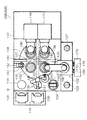
次に、ウェーハマウント装置10Dの構成について説明する。図9はウェーハマウント装置10Dの構成を模式的に表した平面図である。図10は、UV光照射後のウェーハマウント装置10Dの動作順序を模式的に示した側面図である。
Next, the configuration of the
ウェーハマウント装置10Dは、テープマウント(テープマウント手段)11、テープリムーバ(テープ剥離手段)12、及びテープエキスパンダ(エキスパンド手段)13、プラズマ洗浄装置(洗浄手段)19、UV照射装置(照射手段)18を備えている。更に、テープマウント11近傍にはフレームストッカー(フレーム供給手段)15、エキスパンダ13近傍にはリングストッカー(保持リング供給手段)17、及びカセットストッカー(ウェーハ収納手段)14がそれぞれ設けられている。
The
ウェーハマウント装置10Dへは、全面吸着式の搬送装置41の吸着パッド42により、レーザーダイシング後のウェーハWが搬送されてくる。ウェーハWは、既述したように、表面に形成されたパターンを保護する保護用シート21が貼着され、裏面を平坦に研削及び研磨された後にレーザーダイシングされたものであり、保護用シート21が貼着された表面側を下に向けて吸着パッド42に吸着されるようになっている。
The wafer W after laser dicing is transferred to the
搬送装置41によりウェーハマウント装置10Dへ搬送されてきたウェーハWは、先ず、プラズマ洗浄装置19へ搬送される。プラズマ洗浄装置19は、酸素、水素等のプラズマを発生させてウェーハWへ当て、ウェーハW上に残る有機汚染物を除去し、レーザーダイシングにより形成された改質領域の質を改善する。これにより、エキスパンド時の欠けの発生を抑える。プラズマ洗浄装置19としては、例えば松下電工株式会社製大気圧プラズマクリーニング装置(製品名:Aiplasma)等が好適に利用可能である。
The wafer W transferred to the
プラズマ洗浄装置19により洗浄されたウェーハWは、UV照射装置18へ搬送される。UV照射装置18は、図11に示されるように、複数のUV発光管26、26…がケース27内に平行に並べられ、上方に向けて紫外線光を照射するようになっている。
The wafer W cleaned by the
ウェーハWは、UV照射装置18上を搬送装置41により搬送されて通過する際に、保護用シート21が貼着された表面にUV光が照射され、貼着された保護用シート21の粘着力が低下する。これにより、保護用シート21の剥離が容易になる。
When the wafer W is transported by the
なお、UV照射装置18は、ケース27内に平行にUV発光管26を並べた構造で説明したが、この構造に限らず、図18に示されるUV照射装置18Aのように、断面凹面形状の反射板28を有し、中央部に設けられたUV発光管26から照射されたUV光を上方へ平行に反射する構造等、様々な構造が適用可能である。
The
UV照射装置18を通過したウェーハWは、テーブル16まで搬送され、図10(a)に示されるように、保護用シート21が貼着された表面側を下にしてテーブル16に載置されるようになっている。
The wafer W that has passed through the
テーブル16には、不図示の真空吸着機構が設けられており、フレームストッカー15から搬送装置31のアーム32により供給されるフレームF(図16参照)とウェーハWとを吸着する。テーブル16は、不図示の駆動装置によりガイド36に沿って移動し、テープマウント11の下方を通過するようになっている。
The table 16 is provided with a vacuum suction mechanism (not shown), and sucks the frame F (see FIG. 16) and the wafer W supplied from the
テープマウント11は、ガイド36の上方に位置し、テーブル16上に吸着載置されたウェーハWの裏面側へ、図10(b)及び(c)に示されるように、ダイシングテープ22によりフレームFをマウントするようになっている。
The
テープマウント11において、ダイシングテープ22が供給リール37に巻きつけられており、ダイシングテープ22が不図示のガイドリールを経て、ウェーハWに対して平行に広がるように巻取りリール38へ巻き取られるようになっている。
In the
ウェーハWをダイシングテープ22によりフレームFへマウントする際には、テープマウント11の下方に位置したフレームFとウェーハWとへ、テープマウント11に設けられた不図示のローラによりダイシングテープ22を押圧して貼着することによりマウントする。
When the wafer W is mounted on the frame F with the dicing
このとき、ウェーハWとダイシングテープ22との間には、ダイシングされたチップと基板とを接合する際に使用されるダイアタッチフィルム23(以下、DAFと称する)が貼着される。これにより、ダイボンディングを行う工程が簡略化され、スループットの向上が可能となる。
At this time, a die attach film 23 (hereinafter referred to as DAF) used when bonding the diced chip and the substrate is attached between the wafer W and the dicing
ダイシングテープ22を貼着した後は、テープマウント11に設けられた不図示のカッターにより不要な部分が切断除去されるようになっている。
After the dicing
テープリムーバ12は、図10(d)に示されるように、ダイシングテープ22によりフレームFがマウントされたウェーハWの表面より保護シート21を剥離するようになっている。
As shown in FIG. 10 (d), the
フレームFがマウントされたウェーハWは、テーブル16から搬送装置39によりテープリムーバ12上へ保護シート21が貼着された表面側が上となるように反転させながら搬送され、不図示のアームにより保護シート21が剥離されるようになっている。保護シート21は、UV照射装置18により照射されたUV光により粘着力が低下されているため、ウェーハW上から容易に剥離することが可能である。
The wafer W on which the frame F is mounted is transferred from the table 16 to the
エキスパンダ13は、リングストッカー17から搬送装置33のアーム34により供給される保持リングRを、フレームFにマウントされたウェーハWのダイシングテープ22側より押圧し、ダイシングされたウェーハWのエキスパンドを行う装置である。
The
このエキスパンダ13へは、搬送装置39により保護シート21が剥離された後のウェーハWが搬送される。エキスパンダ13は、図10(e)に示されるように、フレームFをフレーム固定機構25により固定し、保持リングRを押し上げ機構24によりダイシングテープ22へ押圧してダイシングテープ22を放射状にエキスパンドする装置である。これにより、ウェーハWは個々のチップTに分割される。
The wafer W after the
保持リングRはフレームFに嵌合してエキスパンド状態を保持するためのリングである。エキスパンド後のウェーハWは、保持リングRごと搬送装置39によりテープリムーバ12側へ戻される。テープリムーバ12上のエキスパンド後のウェーハWは、不図示の移動手段によってガイド35上を移動し、図10(f)に示されるように、カセットストッカー14に載置されたカセットC内へ順次収納されるようになっている。
The holding ring R is a ring for fitting into the frame F to hold the expanded state. The expanded wafer W is returned to the
カセットストッカー14は、カセットCを載置して上下するエレベータを備え、ウェーハWを収納する位置を順次変更していく収納装置である。そして、カセットCの全ての収納位置へウェーハWが収納された時点で、不図示の搬送装置によりカセットCをウェーハマウント装置10から搬出し、新しいカセットCがカセットストッカー14へセットされるようになっている。
The
次に、本発明に係るウェーハ加工方法の実際の手順について説明する。図12はウェーハ加工方法の動作順序を示したフロー図である。ウェーハWの加工は、図1等により既述したウェーハ加工装置10を使用して行われる。
Next, the actual procedure of the wafer processing method according to the present invention will be described. FIG. 12 is a flowchart showing the operation sequence of the wafer processing method. The wafer W is processed using the
先ず、平面加工装置10Aを使用して、ウェーハWの裏面を加工し(研削及び研磨)、厚さT2まで加工する(ステップS10)。すなわち、第1の機械加工ステップにおいて、ウェーハの最終加工厚さT1より50〜500μm厚い厚さT2までウェーハの裏面を加工する。これにより、ダイシング後のウェーハWの機械的強度が大幅に向上する。したがって、ダイシング後に各工程に使用される装置間を搬送される際、多少の衝撃や振動を受けても、内部の改質領域Kを起点として割段されてしまうような不具合は激減又は皆無となる。
First, using the
この厚さT2は、最終加工厚さT1より100〜300μm厚いことがより好ましく、最終加工厚さT1より150〜250μm厚いことが更に好ましい。 The thickness T2 is more preferably 100 to 300 μm thicker than the final processed thickness T1, and more preferably 150 to 250 μm thicker than the final processed thickness T1.
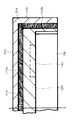
図13は、表面(下面)に既述の保護用シート21が貼着されたウェーハWの断面図である。同図において、ウェーハWは、裏面が加工された後に最終加工厚さT1より厚い厚さT2になっている。
FIG. 13 is a cross-sectional view of the wafer W having the above-described
次いで、レーザーダイシング装置10B使用して、ウェーハWの裏面(上面)よりレーザー光Lを照射して、ウェーハWの内部へ改質領域K、K…を形成する(ステップS20)。この改質領域K、K…のウェーハWの厚さ方向の位置は、ウェーハの表面(下面)より厚さ方向にT1までの距離の位置であることが好ましい。このような厚さ方向に改質領域が形成されれば、ウェーハの割断が容易となる。
Next, the
次いで、平面加工装置10Cを使用して、ウェーハWの裏面を加工し(研削及び研磨)、最終加工厚さT1まで加工する(ステップS30)。 Next, the back surface of the wafer W is processed (grinding and polishing) using the planar processing apparatus 10C and processed to the final processing thickness T1 (step S30).
次いで、プラズマ洗浄装置19を使用して、ウェーハW上に残る有機汚染物を除去する(ステップS40)。 Next, organic contaminants remaining on the wafer W are removed using the plasma cleaning device 19 (step S40).
次いで、ウェーハマウント装置10Dを使用して、ウェーハWの各チップ間の間隔を拡張する(ステップS50)。以下、このエキスパンドステップについて図14により説明する。図14は、ウェーハマウント装置の動作順序を示したフロー図である。なお、既述の図10は、UV光照射後のウェーハマウント装置10Dの動作順序を模式的に示した側面図でもある。
Next, the distance between the chips of the wafer W is expanded using the
まず、ステップS40(前工程)において、ウェーハWがプラズマ洗浄される。 First, in step S40 (previous process), the wafer W is plasma-cleaned.
そして、ウェーハWが、全面吸着型の搬送装置41により保護用シート21側を下方に向けて吸着されて搬送され、UV照射装置18から保護用シート21へ向けてUV光が照射され、保護用シート21の粘着力を低下させる(ステップS51)。
Then, the wafer W is sucked and transported by the entire surface suction-
次いで、ダイシングテープ22がウェーハWの裏面とフレームFへ貼着され、不要部分が切断されてウェーハWがフレームFへマウントされる(ステップS52)。
Next, the dicing
フレームFへマウントされたウェーハWは、搬送装置39により反転され、表面に貼着された保護シート21が剥離される(ステップS53)。
The wafer W mounted on the frame F is reversed by the
ウェーハWは、エキスパンダ13に搬送され、保持リングRがダイシングテープ22側から押圧され、ウェーハWのエキスパンドが行われる(ステップS54)。
The wafer W is transferred to the
エキスパンドされたウェーハWは、カセットストッカー14に載置されたカセットCへ保持リングRごと順次収納されていく(ステップS55)。 The expanded wafer W is sequentially stored together with the holding ring R in the cassette C placed on the cassette stocker 14 (step S55).
以上説明したように、本発明に係るウェーハ加工方法によれば、レーザーダイシング装置によりダイシングされたウェーハを、ダメージを与えることなくチップに分割することができる。 As described above, according to the wafer processing method of the present invention, the wafer diced by the laser dicing apparatus can be divided into chips without causing damage.
10…ウェーハ加工装置、10A、10C…平面加工装置、10B…レーザーダイシング装置、10D…ウェーハマウント装置、11…テープマウント(テープマウント手段)、12…テープリムーバ(テープ剥離手段)、13…テープエキスパンダ(エキスパンド手段)、14…カセットストッカー、15…フレームストッカー(ダイシングフレーム供給手段)、16…テーブル、17…リングストッカー(保持リング供給手段)、18、18A…UV照射装置(照射手段)、21…保護シート、22…ダイシングテープ、23…ダイアタッチフィルム(DAF)、114…カセット収納ステージ、116…アライメントステージ、118…粗研削ステージ、120…精研削ステージ、122…研磨ステージ、123…研磨布洗浄ステージ、124…ウェーハ洗浄ステージ、231…レーザーヘッド、231D…コンデンスレンズ、L…レーザー光、C…カセット、F…フレーム、K…改質領域、R…保持リング、W…ウェーハ
DESCRIPTION OF
Claims (4)
第1の機械加工後の前記ウェーハにレーザー光を照射して内部へ改質領域を形成する改質領域形成ステップと、
改質領域形成後の前記ウェーハの裏面を研削加工し、研削後の前記ウェーハの裏面を研磨加工し、ウェーハの最終加工厚さT1まで前記ウェーハの裏面を加工する第2の機械加工ステップと、
を備えることを特徴とするウェーハ加工方法。 A first machining step of grinding the back surface of the wafer, polishing the back surface of the wafer after grinding, and processing the back surface of the wafer to a thickness T2 that is 50 to 500 μm thicker than a final processing thickness T1 of the wafer; ,
A modified region forming step of irradiating the wafer after the first machining with a laser beam to form a modified region therein;
A second machining step of grinding the back surface of the wafer after forming the modified region, polishing the back surface of the wafer after grinding, and processing the back surface of the wafer to a final processing thickness T1 of the wafer;
A wafer processing method comprising:
第2の機械加工後の前記ウェーハの表面に紫外線光を照射する紫外線光照射ステップと、
紫外線光照射後の前記ウェーハの裏面にダイシングテープを貼着して前記ウェーハをフレームへマウントするテープマウントステップと、
フレームへマウントされた前記ウェーハの表面に貼着されている前記保護用テープの剥離を行うテープ剥離ステップと、
前記保護用テープが剥離された前記ウェーハの前記ダイシングテープが貼着された側より、前記ダイシングテープのエキスパンドを行い、前記ウェーハの各チップ間の間隔を拡張するエキスパンドステップと、
を備える請求項1に記載のウェーハ加工方法。 A tape adhering step of adhering a protective tape for protecting the pattern formed on the surface of the wafer to the surface of the wafer before the first machining;
An ultraviolet light irradiation step of irradiating the surface of the wafer after the second machining with ultraviolet light;
A tape mounting step of attaching a dicing tape to the back surface of the wafer after irradiation with ultraviolet light and mounting the wafer on a frame;
A tape peeling step for peeling off the protective tape attached to the surface of the wafer mounted on a frame;
An expanding step for expanding the dicing tape from the side where the dicing tape is attached to the wafer from which the protective tape has been peeled off, and expanding the interval between the chips of the wafer;
The wafer processing method of Claim 1 provided with.
Priority Applications (5)
| Application Number | Priority Date | Filing Date | Title |
|---|---|---|---|
| JP2006058330A JP2007235068A (en) | 2006-03-03 | 2006-03-03 | Wafer machining method |
| DE112007000520T DE112007000520T5 (en) | 2006-03-03 | 2007-02-16 | Wafer processing method |
| US12/281,590 US20090011571A1 (en) | 2006-03-03 | 2007-02-16 | Wafer working method |
| KR1020087021346A KR20080098633A (en) | 2006-03-03 | 2007-02-16 | Wafer processing method |
| PCT/JP2007/052825 WO2007099787A1 (en) | 2006-03-03 | 2007-02-16 | Wafer processing method |
Applications Claiming Priority (1)
| Application Number | Priority Date | Filing Date | Title |
|---|---|---|---|
| JP2006058330A JP2007235068A (en) | 2006-03-03 | 2006-03-03 | Wafer machining method |
Publications (2)
| Publication Number | Publication Date |
|---|---|
| JP2007235068A true JP2007235068A (en) | 2007-09-13 |
| JP2007235068A5 JP2007235068A5 (en) | 2009-04-02 |
Family
ID=38458900
Family Applications (1)
| Application Number | Title | Priority Date | Filing Date |
|---|---|---|---|
| JP2006058330A Pending JP2007235068A (en) | 2006-03-03 | 2006-03-03 | Wafer machining method |
Country Status (5)
| Country | Link |
|---|---|
| US (1) | US20090011571A1 (en) |
| JP (1) | JP2007235068A (en) |
| KR (1) | KR20080098633A (en) |
| DE (1) | DE112007000520T5 (en) |
| WO (1) | WO2007099787A1 (en) |
Cited By (13)
| Publication number | Priority date | Publication date | Assignee | Title |
|---|---|---|---|---|
| WO2009069509A1 (en) * | 2007-11-30 | 2009-06-04 | Hamamatsu Photonics K.K. | Working object grinding method |
| JP2011171382A (en) * | 2010-02-16 | 2011-09-01 | Disco Corp | Dividing method |
| JP2013008831A (en) * | 2011-06-24 | 2013-01-10 | Disco Abrasive Syst Ltd | Processing method of wafer |
| JP2014209523A (en) * | 2013-04-16 | 2014-11-06 | 株式会社ディスコ | Wafer processing method |
| JP2014212282A (en) * | 2013-04-22 | 2014-11-13 | 株式会社ディスコ | Processing method of wafer |
| DE102017011495A1 (en) | 2017-01-10 | 2018-07-12 | Fanuc Corporation | Combined machining method and combined machining program |
| JP2019012850A (en) * | 2018-10-03 | 2019-01-24 | 株式会社東京精密 | Wafer processing method and wafer processing system |
| JP2019169719A (en) * | 2019-04-25 | 2019-10-03 | 株式会社東京精密 | Laser processing system |
| JP2019192937A (en) * | 2019-07-05 | 2019-10-31 | 株式会社東京精密 | Wafer processing system and wafer processing method |
| JP2020088323A (en) * | 2018-11-30 | 2020-06-04 | 株式会社ディスコ | Wafer manufacturing device |
| WO2023210088A1 (en) * | 2022-04-27 | 2023-11-02 | ヤマハ発動機株式会社 | Wafer processing device, manufacturing method for semiconductor chip, and semiconductor chip |
| WO2023209871A1 (en) * | 2022-04-27 | 2023-11-02 | ヤマハ発動機株式会社 | Wafer processing apparatus, method for manufacturing semiconductor chip, and semiconductor chip |
| JP7434463B2 (en) | 2017-08-28 | 2024-02-20 | リンテック株式会社 | Substrate transfer system and substrate transfer method |
Families Citing this family (2)
| Publication number | Priority date | Publication date | Assignee | Title |
|---|---|---|---|---|
| CN105742329A (en) * | 2016-03-07 | 2016-07-06 | 京东方科技集团股份有限公司 | Display panel and manufacturing method therefor, and display apparatus |
| JP7157301B2 (en) * | 2017-11-06 | 2022-10-20 | 株式会社東京精密 | Wafer processing method |
Citations (4)
| Publication number | Priority date | Publication date | Assignee | Title |
|---|---|---|---|---|
| WO2003077295A1 (en) * | 2002-03-12 | 2003-09-18 | Hamamatsu Photonics K.K. | Method for dicing substrate |
| JP2004241443A (en) * | 2003-02-03 | 2004-08-26 | Sanyo Electric Co Ltd | Manufacturing method of semiconductor apparatus |
| JP2004349623A (en) * | 2003-05-26 | 2004-12-09 | Disco Abrasive Syst Ltd | Partitioning method of nonmetallic substrate |
| JP2005302982A (en) * | 2004-04-12 | 2005-10-27 | Nitto Denko Corp | Process for producing semiconductor chip |
Family Cites Families (10)
| Publication number | Priority date | Publication date | Assignee | Title |
|---|---|---|---|---|
| JP3626442B2 (en) | 2000-09-13 | 2005-03-09 | 浜松ホトニクス株式会社 | Laser processing method |
| JP2002192371A (en) | 2000-09-13 | 2002-07-10 | Hamamatsu Photonics Kk | Laser beam machining method and laser beam machining device |
| JP3408805B2 (en) | 2000-09-13 | 2003-05-19 | 浜松ホトニクス株式会社 | Cutting origin region forming method and workpiece cutting method |
| JP3722731B2 (en) | 2000-09-13 | 2005-11-30 | 浜松ホトニクス株式会社 | Laser processing method |
| JP4762458B2 (en) | 2000-09-13 | 2011-08-31 | 浜松ホトニクス株式会社 | Laser processing equipment |
| JP4659300B2 (en) | 2000-09-13 | 2011-03-30 | 浜松ホトニクス株式会社 | Laser processing method and semiconductor chip manufacturing method |
| US20030064579A1 (en) * | 2001-09-27 | 2003-04-03 | Masafumi Miyakawa | Surface protecting adhesive film for semiconductor wafer and protecting method for semiconductor wafer using said adhesive film |
| WO2003076118A1 (en) * | 2002-03-12 | 2003-09-18 | Hamamatsu Photonics K.K. | Semiconductor substrate, semiconductor chip, and semiconductor device manufacturing method |
| KR100486290B1 (en) * | 2002-12-23 | 2005-04-29 | 삼성전자주식회사 | Assembling method of semiconductor package and removal apparatus of protection tape in semiconductor process |
| JPWO2006008824A1 (en) * | 2004-07-16 | 2008-05-01 | 株式会社ルネサステクノロジ | Manufacturing method of semiconductor integrated circuit device |
-
2006
- 2006-03-03 JP JP2006058330A patent/JP2007235068A/en active Pending
-
2007
- 2007-02-16 KR KR1020087021346A patent/KR20080098633A/en not_active Application Discontinuation
- 2007-02-16 WO PCT/JP2007/052825 patent/WO2007099787A1/en active Application Filing
- 2007-02-16 DE DE112007000520T patent/DE112007000520T5/en not_active Withdrawn
- 2007-02-16 US US12/281,590 patent/US20090011571A1/en not_active Abandoned
Patent Citations (4)
| Publication number | Priority date | Publication date | Assignee | Title |
|---|---|---|---|---|
| WO2003077295A1 (en) * | 2002-03-12 | 2003-09-18 | Hamamatsu Photonics K.K. | Method for dicing substrate |
| JP2004241443A (en) * | 2003-02-03 | 2004-08-26 | Sanyo Electric Co Ltd | Manufacturing method of semiconductor apparatus |
| JP2004349623A (en) * | 2003-05-26 | 2004-12-09 | Disco Abrasive Syst Ltd | Partitioning method of nonmetallic substrate |
| JP2005302982A (en) * | 2004-04-12 | 2005-10-27 | Nitto Denko Corp | Process for producing semiconductor chip |
Cited By (19)
| Publication number | Priority date | Publication date | Assignee | Title |
|---|---|---|---|---|
| WO2009069509A1 (en) * | 2007-11-30 | 2009-06-04 | Hamamatsu Photonics K.K. | Working object grinding method |
| JP2009131942A (en) * | 2007-11-30 | 2009-06-18 | Hamamatsu Photonics Kk | Grinding method of machining object |
| EP2236243A1 (en) * | 2007-11-30 | 2010-10-06 | Hamamatsu Photonics K.K. | Working object grinding method |
| US8523636B2 (en) | 2007-11-30 | 2013-09-03 | Hamamatsu Photonics K.K. | Working object grinding method |
| EP2236243A4 (en) * | 2007-11-30 | 2013-10-23 | Hamamatsu Photonics Kk | Working object grinding method |
| JP2011171382A (en) * | 2010-02-16 | 2011-09-01 | Disco Corp | Dividing method |
| JP2013008831A (en) * | 2011-06-24 | 2013-01-10 | Disco Abrasive Syst Ltd | Processing method of wafer |
| JP2014209523A (en) * | 2013-04-16 | 2014-11-06 | 株式会社ディスコ | Wafer processing method |
| JP2014212282A (en) * | 2013-04-22 | 2014-11-13 | 株式会社ディスコ | Processing method of wafer |
| DE102017011495A1 (en) | 2017-01-10 | 2018-07-12 | Fanuc Corporation | Combined machining method and combined machining program |
| US10695871B2 (en) | 2017-01-10 | 2020-06-30 | Fanuc Corporation | Combined machining method and computer readable medium |
| JP7434463B2 (en) | 2017-08-28 | 2024-02-20 | リンテック株式会社 | Substrate transfer system and substrate transfer method |
| JP2019012850A (en) * | 2018-10-03 | 2019-01-24 | 株式会社東京精密 | Wafer processing method and wafer processing system |
| JP2020088323A (en) * | 2018-11-30 | 2020-06-04 | 株式会社ディスコ | Wafer manufacturing device |
| JP2019169719A (en) * | 2019-04-25 | 2019-10-03 | 株式会社東京精密 | Laser processing system |
| JP2019192937A (en) * | 2019-07-05 | 2019-10-31 | 株式会社東京精密 | Wafer processing system and wafer processing method |
| WO2023210088A1 (en) * | 2022-04-27 | 2023-11-02 | ヤマハ発動機株式会社 | Wafer processing device, manufacturing method for semiconductor chip, and semiconductor chip |
| WO2023209871A1 (en) * | 2022-04-27 | 2023-11-02 | ヤマハ発動機株式会社 | Wafer processing apparatus, method for manufacturing semiconductor chip, and semiconductor chip |
| WO2023209897A1 (en) * | 2022-04-27 | 2023-11-02 | ヤマハ発動機株式会社 | Wafer machining device, method for manufacturing semiconductor chip, and semiconductor chip |
Also Published As
| Publication number | Publication date |
|---|---|
| US20090011571A1 (en) | 2009-01-08 |
| WO2007099787A1 (en) | 2007-09-07 |
| KR20080098633A (en) | 2008-11-11 |
| DE112007000520T5 (en) | 2009-01-15 |
Similar Documents
| Publication | Publication Date | Title |
|---|---|---|
| JP2007235069A (en) | Wafer machining method | |
| JP2007235068A (en) | Wafer machining method | |
| JP2007214457A (en) | Wafer processing equipment and method therefor | |
| US10755946B2 (en) | Method for producing a wafer from a hexagonal single crystal ingot by applying a laser beam to form a first production history, an exfoliation layer, and a second production history | |
| JP5953645B2 (en) | Semiconductor substrate cutting method and semiconductor substrate cutting apparatus | |
| JP2002343756A (en) | Water planarizing apparatus | |
| TW201904703A (en) | Wafer producing apparatus | |
| JP2008155292A (en) | Method and apparatus for machining substrate | |
| JP6137798B2 (en) | Laser processing apparatus and protective film coating method | |
| JP2007201179A (en) | Device and method for mounting wafer | |
| JP2019012849A (en) | Wafer processing method and wafer processing system | |
| JP6081006B2 (en) | Wafer cleaving method and wafer cleaving apparatus | |
| JP6327490B2 (en) | Wafer processing apparatus and wafer processing method | |
| JP2019012848A (en) | Wafer processing method and wafer processing system | |
| JP2011031359A (en) | Polishing tool, polishing device, and polishing machining method | |
| JP6593663B2 (en) | Wafer processing method and wafer processing system | |
| JP2012121085A (en) | Grinding device | |
| JP6249318B2 (en) | Manufacturing system and manufacturing method of thin chip having high bending strength | |
| JP6081005B2 (en) | Grinding / polishing apparatus and grinding / polishing method | |
| JP2019169719A (en) | Laser processing system | |
| JP2019068077A (en) | Laser processing device and laser processing method | |
| JP2019012850A (en) | Wafer processing method and wafer processing system | |
| JP2018142717A (en) | Wafer processing method and wafer processing system | |
| JP6979608B2 (en) | Grinding device and grinding method | |
| JP2017092503A (en) | Wafer dividing system and wafer dividing method |
Legal Events
| Date | Code | Title | Description |
|---|---|---|---|
| A521 | Written amendment |
Free format text: JAPANESE INTERMEDIATE CODE: A523 Effective date: 20090216 |
|
| A621 | Written request for application examination |
Free format text: JAPANESE INTERMEDIATE CODE: A621 Effective date: 20090216 |
|
| A131 | Notification of reasons for refusal |
Free format text: JAPANESE INTERMEDIATE CODE: A131 Effective date: 20110809 |
|
| A521 | Written amendment |
Free format text: JAPANESE INTERMEDIATE CODE: A523 Effective date: 20111011 |
|
| A02 | Decision of refusal |
Free format text: JAPANESE INTERMEDIATE CODE: A02 Effective date: 20120217 |