JP2007234232A - Image display device - Google Patents
Image display device Download PDFInfo
- Publication number
- JP2007234232A JP2007234232A JP2006050624A JP2006050624A JP2007234232A JP 2007234232 A JP2007234232 A JP 2007234232A JP 2006050624 A JP2006050624 A JP 2006050624A JP 2006050624 A JP2006050624 A JP 2006050624A JP 2007234232 A JP2007234232 A JP 2007234232A
- Authority
- JP
- Japan
- Prior art keywords
- light emitting
- emitting layer
- display device
- image display
- organic light
- Prior art date
- Legal status (The legal status is an assumption and is not a legal conclusion. Google has not performed a legal analysis and makes no representation as to the accuracy of the status listed.)
- Pending
Links
Images


Classifications
-
- F—MECHANICAL ENGINEERING; LIGHTING; HEATING; WEAPONS; BLASTING
- F21—LIGHTING
- F21K—NON-ELECTRIC LIGHT SOURCES USING LUMINESCENCE; LIGHT SOURCES USING ELECTROCHEMILUMINESCENCE; LIGHT SOURCES USING CHARGES OF COMBUSTIBLE MATERIAL; LIGHT SOURCES USING SEMICONDUCTOR DEVICES AS LIGHT-GENERATING ELEMENTS; LIGHT SOURCES NOT OTHERWISE PROVIDED FOR
- F21K2/00—Non-electric light sources using luminescence; Light sources using electrochemiluminescence
- F21K2/06—Non-electric light sources using luminescence; Light sources using electrochemiluminescence using chemiluminescence
-
- H—ELECTRICITY
- H10—SEMICONDUCTOR DEVICES; ELECTRIC SOLID-STATE DEVICES NOT OTHERWISE PROVIDED FOR
- H10K—ORGANIC ELECTRIC SOLID-STATE DEVICES
- H10K59/00—Integrated devices, or assemblies of multiple devices, comprising at least one organic light-emitting element covered by group H10K50/00
- H10K59/10—OLED displays
- H10K59/12—Active-matrix OLED [AMOLED] displays
- H10K59/122—Pixel-defining structures or layers, e.g. banks
-
- H—ELECTRICITY
- H10—SEMICONDUCTOR DEVICES; ELECTRIC SOLID-STATE DEVICES NOT OTHERWISE PROVIDED FOR
- H10K—ORGANIC ELECTRIC SOLID-STATE DEVICES
- H10K59/00—Integrated devices, or assemblies of multiple devices, comprising at least one organic light-emitting element covered by group H10K50/00
- H10K59/30—Devices specially adapted for multicolour light emission
- H10K59/35—Devices specially adapted for multicolour light emission comprising red-green-blue [RGB] subpixels
-
- H—ELECTRICITY
- H10—SEMICONDUCTOR DEVICES; ELECTRIC SOLID-STATE DEVICES NOT OTHERWISE PROVIDED FOR
- H10K—ORGANIC ELECTRIC SOLID-STATE DEVICES
- H10K2102/00—Constructional details relating to the organic devices covered by this subclass
- H10K2102/301—Details of OLEDs
- H10K2102/351—Thickness
Abstract
Description
本発明は、一対の電極間に発光層を設け、一対の電極により発光層に電界を印加させて発光させる複数の発光素子を有する画像表示装置に係わり、特に発光素子の非発光部としての隔壁に起因する混色の発生を抑制させる隔壁の構造に関するものである。 The present invention relates to an image display device having a light emitting layer provided between a pair of electrodes, and having a plurality of light emitting elements that emit light by applying an electric field to the light emitting layer by the pair of electrodes, and in particular, a partition as a non-light emitting portion of the light emitting element It is related with the structure of the partition which suppresses generation | occurrence | production of the color mixture resulting from this.
近年、フラットパネル型の表示装置として液晶表示装置(LCD)やプラズマ表示装置(PDP)、電子放出型表示装置(FED)、有機発光表示装置(OLED)などが実用化ないし実用化研究段階にある。その中でも、有機発光表示装置は、薄型・軽量の自発光型表示装置の典型としてこれからの表示装置として極めて有望な表示装置である。有機発光表示装置には、所謂ボトムエミッション型とトップエミッション型とがある。 In recent years, liquid crystal display devices (LCD), plasma display devices (PDP), electron emission display devices (FED), organic light emitting display devices (OLED), etc. are in practical application or practical application research stage as flat panel display devices. . Among them, the organic light emitting display device is a very promising display device as a future display device as a typical thin and light self-luminous display device. The organic light emitting display device includes a so-called bottom emission type and a top emission type.
ボトムエミッション型の有機発光表示装置は、ガラス基板を好適とする透光性基板上に第1の電極または一方の電極としての透光性電極と、電界の印加により発光する有機発光層(有機多層膜とも言う)と、第2の電極または他方の電極としての反射性金属電極とを順次積層した発光機構により有機発光素子が構成される。この有機発光素子をマトリクス状に多数配列し、それらの積層構造を覆って封止缶とも称する絶縁性基板により封着させて上記発光構造を外部の雰囲気から遮断している。 A bottom emission type organic light-emitting display device includes a light-transmitting electrode as a first electrode or one electrode on a light-transmitting substrate, preferably a glass substrate, and an organic light-emitting layer that emits light when an electric field is applied (organic multilayer). An organic light-emitting element is configured by a light-emitting mechanism in which a second electrode or a reflective metal electrode as the other electrode is sequentially stacked. A large number of organic light-emitting elements are arranged in a matrix, and the laminated structure is covered and sealed with an insulating substrate, which is also called a sealing can, thereby blocking the light-emitting structure from the external atmosphere.
そして、例えば透光性電極を陽極とし、反射性金属電極を陰極として両者の電極間に電界を印加することにより、有機発光層にキャリア(電子と正孔)が注入され、この有機発光層が発光する。この発光光を透光性基板側から外部に出射する構成となっている。 Then, for example, carriers (electrons and holes) are injected into the organic light emitting layer by applying an electric field between the two electrodes using the translucent electrode as the anode and the reflective metal electrode as the cathode. Emits light. This emitted light is configured to be emitted from the translucent substrate side to the outside.
一方、トップエミッション型の有機発光表示装置は、上述した一方の電極を反射性金属電極とし、他方の電極を透光性電極として両者の電極間に電界を印加することにより、有機発光層が発光し、この発光を上述した他方の電極(透光性電極)側から出射する構成となっている。トップエミッション型では、ボトムエミッション型における封止缶として透光性基板が使用される。 On the other hand, in the top emission type organic light emitting display device, the organic light emitting layer emits light by applying an electric field between the two electrodes by using one electrode as a reflective metal electrode and the other electrode as a translucent electrode. The light emission is emitted from the other electrode (translucent electrode) side described above. In the top emission type, a translucent substrate is used as a sealing can in the bottom emission type.
この種の有機発光表示装置において、それぞれが異なる色を発色する有機発光素子を複数個備えた多色表示有機発光表示装置では、従来から赤,緑,青の3原色で発光する有機材料をマトリックス状に配置することが行われている。3原色の有機材料を高精度にマトリックス状に配置することが必要であることから、複雑な光露光プロセスやエッチングプロセス等が必須となっていた。そこで、3原色の有機材料の配置を簡便に行うために予めバンク(隔壁)を形成しておき、このバンクを利用して有機材料のパターニングを行う手段が用いられている。 In this type of organic light emitting display device, in a multicolor display organic light emitting display device having a plurality of organic light emitting elements that emit different colors, an organic material that emits light in three primary colors of red, green, and blue is conventionally used as a matrix. It is done to arrange in the shape. Since it is necessary to arrange the organic materials of the three primary colors in a matrix with high accuracy, a complicated light exposure process, etching process, and the like have been essential. Therefore, in order to easily arrange the organic materials of the three primary colors, a bank (partition wall) is formed in advance, and means for patterning the organic material using this bank is used.
このように3原色の有機材料を区画するバンクの構造としては、特開2003−229256号公報(特許文献1)に開示されているようにバンクの形状を格子状に形成し、この格子状バンクの縦横を同じ厚さとすることが記載されている。また、他のバンク構造としては、特開2005−71656号公報(特許文献2)に開示されているようにバンクの形状を格子状に形成せずに、ストライプ状に形成することが記載されている。 As a bank structure for partitioning the organic materials of the three primary colors in this way, the bank shape is formed in a lattice shape as disclosed in Japanese Patent Laid-Open No. 2003-229256 (Patent Document 1). It is described that the vertical and horizontal thicknesses are the same. In addition, as another bank structure, as disclosed in Japanese Patent Laid-Open No. 2005-71656 (Patent Document 2), it is described that the bank shape is not formed in a lattice shape but is formed in a stripe shape. Yes.
しかしながら、特許文献1に開示された有機EL装置は、格子状バンクの縦横を同じ厚さとする構造とすることにより、バンクの高さを超える量の有機材料がバンクで囲まれた領域に供給されると、バンクを越えて隣接する画素領域にその有機材料が広がってしまう。有機材料が異なる色を発光する発光層である場合にこのような状態が発生すると、電気特性や発光スペクトルが変化してしまう。また、バンクで囲まれた領域にCF(カラーフィルタ)層やCCM(色変換方式)層を形成する場合にこのような状態が発生すると、発光スペクトルが変化してしまうという課題があった。 However, in the organic EL device disclosed in Patent Document 1, an amount of organic material exceeding the bank height is supplied to a region surrounded by the bank by adopting a structure in which the length and width of the lattice bank are the same. Then, the organic material spreads beyond the bank to the adjacent pixel region. If such a state occurs when the organic material is a light emitting layer that emits different colors, the electrical characteristics and emission spectrum will change. Further, when a CF (color filter) layer or a CCM (color conversion method) layer is formed in a region surrounded by the bank, there is a problem that an emission spectrum changes when such a state occurs.
また、特許文献2に開示された有機ELディスプレイは、格子状にバンクを設けずにストライプ状にバンクを形成することにより、格子状に形成した場合に比較して多量の有機材料が必要になるのみならず、画素電極の縦端部においてリーク電流が発生し、発光効率の低下が懸念される。また、有機発光層で発光した光が画面に出て行かないために光利用効率が低下してしまうという課題があった。 Further, the organic EL display disclosed in Patent Document 2 requires a larger amount of organic material than the case where the organic EL display is formed in a lattice shape by forming the bank in a stripe shape without providing the bank in the lattice shape. In addition, a leak current is generated at the vertical end of the pixel electrode, and there is a concern that the light emission efficiency may be reduced. Moreover, since the light emitted from the organic light emitting layer does not go out to the screen, there is a problem that the light use efficiency is lowered.
したがって、本発明は、前述した従来の課題を解決するためになされたものであり、その目的は、光利用効率を低下させることなく、混色の発生を抑制した有機発光表示装置を提供することにある。 Accordingly, the present invention has been made to solve the above-described conventional problems, and an object of the present invention is to provide an organic light emitting display device that suppresses the occurrence of color mixing without reducing the light utilization efficiency. is there.
このような目的を達成するために本発明による画像表示装置は、格子(井桁)状の隔壁に囲まれた領域に複数の発光素子を備え、当該発光素子の発光によりストライプ状の同色画素が並んで設置される画像表示装置において、同色画素間の隔壁の高さが異色画素間の隔壁の高さよりも低く形成することにより、同色画素形成時に互いに隣接する異色画素への濡れ広がりが抑止されるので、背景技術の課題を解決することができる。 In order to achieve such an object, the image display device according to the present invention includes a plurality of light emitting elements in a region surrounded by a grid (cross-beam) -shaped partition wall, and stripe-like pixels of the same color are arranged by light emission of the light emitting elements. In the image display device installed in the above, by forming the height of the partition walls between the same color pixels lower than the height of the partition walls between the different color pixels, wetting and spreading to adjacent different color pixels when the same color pixels are formed is suppressed. Therefore, the problems of the background art can be solved.
なお、本発明は、上記各構成及び後述する実施の形態に記載される構成に限定されるものではなく、本発明の技術思想を逸脱することなく、種々の変更が可能であることは言うまでもない。 It should be noted that the present invention is not limited to the configurations described in the above-described configurations and the embodiments described later, and it goes without saying that various modifications can be made without departing from the technical idea of the present invention. .
本発明による画像表示装置によれば、異色画素と隣接する隔壁の高さよりも同色画素と隣接する隔壁の高さを低くすることにより、隣接する画素形成領域に異色画素材料が広がり難くなるので、光利用効率を低下させることなく、混色の発生を抑止することができ、解像度が大幅に増大し、表示品位の高い画像表示得られるという極めて優れた効果を有する。 According to the image display device of the present invention, since the height of the partition wall adjacent to the same color pixel is lower than the height of the partition wall adjacent to the different color pixel, the different color pixel material is difficult to spread in the adjacent pixel formation region. The generation of color mixing can be suppressed without reducing the light utilization efficiency, and the resolution is greatly increased, and an image display with high display quality can be obtained.
以下、本発明の具体的な実施の形態について、実施例の図面を参照して詳細に説明する。なお、以下の実施例では、画像表示装置としてボトムエミッション型の有機発光表示装置を例として説明する。また、有機発光素子には、発光に寄与する部分に使用する有機材料として低分子材料系と高分子材料系とがあるが、本発明はこれらに限定されるものではなく、上記低分子材料系と高分子材料系との双方を混成した有機発光層であってもよい。 Hereinafter, specific embodiments of the present invention will be described in detail with reference to the drawings of the examples. In the following embodiments, a bottom emission type organic light emitting display device will be described as an example of the image display device. In addition, the organic light emitting device includes a low molecular material system and a high molecular material system as organic materials used for a portion that contributes to light emission. However, the present invention is not limited to these, and the above low molecular material system is used. And an organic light emitting layer in which both a polymer material system and a polymer material system are mixed.
低分子材料系の有機発光素子の層構成は、一般的に透光性メイン基板側からアノード電極/ホール注入層/ホール輸送層/発光層/電子輸送層/カソード電極の順である。一方、高分子材料系の有機発光素子の層構成は、一般的に透光性メイン基板側からアノード電極/ホール輸送層/発光層/カソード電極の順である。高分子材料系の有機発光素子の場合には、低分子材料系の有機発光素子のホール注入層/ホール輸送層をホール輸送層が両方の特性を兼ねる場合があり、さらに高分子材料系の有機発光素子では、低分子材料系の有機発光素子の電子輸送層/カソード電極をカソード電極のみで代用する場合がある。また、本発明は、以下の実施例で用いた材料及び組成に限定されるものではない。 The layer structure of the low-molecular-weight organic light emitting element is generally in the order of the anode electrode / hole injection layer / hole transport layer / light emitting layer / electron transport layer / cathode electrode from the translucent main substrate side. On the other hand, the layer structure of the polymer material-based organic light emitting element is generally in the order of the anode electrode / hole transport layer / light emitting layer / cathode electrode from the translucent main substrate side. In the case of a polymer material-based organic light-emitting device, the hole injection layer / hole transport layer of the low-molecular material-based organic light-emitting device may have both characteristics. In the light emitting element, the electron transport layer / cathode electrode of the organic light emitting element of the low molecular material type may be substituted only with the cathode electrode. The present invention is not limited to the materials and compositions used in the following examples.
図1は、本発明に係わる有機発光表示装置の実施例1を説明するための全体構成例を示す図であり、図1(a)は要部平面図、図1(b)は図1(a)のA−A´線に沿って切断した断面図、図1(c)は図1(a)のB−B´線に沿って切断した断面図である。また、図2は図1の斜視図である。また、図3は図1(a)のX方向で切断した薄膜トランジスタ及び走査配線部の要部断面図、図4は図1(a)のX方向で切断したデータ線及び隔壁部の要部断面図、図5は図1(a)のY方向で切断した薄膜トランジスタ,走査配線及び低隔壁部の要部断面図である。 FIG. 1 is a diagram showing an example of the overall configuration for explaining an embodiment 1 of an organic light emitting display device according to the present invention. FIG. 1 (a) is a plan view of an essential part, and FIG. Sectional drawing cut | disconnected along the AA 'line of a), FIG.1 (c) is sectional drawing cut | disconnected along BB' line of Fig.1 (a). FIG. 2 is a perspective view of FIG. 3 is a cross-sectional view of the main part of the thin film transistor and the scanning wiring section cut in the X direction of FIG. 1A, and FIG. 4 is a cross section of the main part of the data line and the partition wall section cut in the X direction of FIG. FIGS. 5A and 5B are cross-sectional views of main parts of the thin film transistor, the scanning wiring, and the low partition wall section cut in the Y direction of FIG.
これらの図において、この有機発光表示装置は、図3乃至図5に示すようにアクティブ・マトリクス型であり、透光性メイン基板SUB側から表示光を出射する所謂ボトムエミッション型の画像表示装置である。 In these drawings, the organic light emitting display device is an active matrix type as shown in FIGS. 3 to 5, and is a so-called bottom emission type image display device that emits display light from the translucent main substrate SUB side. is there.
この有機発光表示装置では、図1及び図2に示すように透光性ガラスを好適とする透光性メイン基板SUBの主面(内面)に格子(井桁)状に成膜された隔壁(バンクとも称する)BNKに囲まれた凹部内にストライプ状に赤色有機発光層OLE(R),緑色有機発光層OLE(G)及び青色有機発光層OLE(B)が並んで配設されている。 In this organic light emitting display device, as shown in FIG. 1 and FIG. 2, barrier ribs (banks) formed in a grid pattern on the main surface (inner surface) of a translucent main substrate SUB preferably made of translucent glass. (Also referred to as a red organic light emitting layer OLE (R), a green organic light emitting layer OLE (G), and a blue organic light emitting layer OLE (B) are arranged in stripes in a recess surrounded by BNK.
この有機発光表示装置は、図3〜図5に示すように透光性ガラスを好適とする透光性メイン基板SUBの主面(内面)にアクティブ素子としての薄膜トランジスタTFTを有し、この薄膜トランジスタTFTで駆動される一方の電極(ここでは陽極)ADと、他方の電極(ここでは陰極)CDとの間にそれぞれ赤色有機発光層OLE(R),緑色有機発光層OLE(G)及び青色有機発光層OLE(B)を挟んで有機発光素子を構成している。 This organic light emitting display device has a thin film transistor TFT as an active element on the main surface (inner surface) of a translucent main substrate SUB suitable for translucent glass as shown in FIGS. The red organic light-emitting layer OLE (R), the green organic light-emitting layer OLE (G), and the blue organic light-emitting layer between one electrode (here, anode) AD and the other electrode (here, cathode) CD An organic light-emitting device is configured with the layer OLE (B) interposed therebetween.
また、これらの赤色有機発光層OLE(R),緑色有機発光層OLE(G)及び青色有機発光層OLE(B)には、それぞれ上記薄膜トランジスタTFTが接続されて画素回路を構成している。これらの薄膜トランジスタTFTは、ポリシリコン半導体層PSIと、電源配線PLと、データ信号配線DLと、図示しない走査信号配線とから構成され、それぞれ複数の層間絶縁層を介して形成されている。 The red organic light emitting layer OLE (R), the green organic light emitting layer OLE (G), and the blue organic light emitting layer OLE (B) are connected to the thin film transistors TFT to constitute a pixel circuit. These thin film transistors TFT are composed of a polysilicon semiconductor layer PSI, a power supply wiring PL, a data signal wiring DL, and a scanning signal wiring (not shown), and are formed via a plurality of interlayer insulating layers.
そして、この薄膜トランジスタTFTを含む画素回路は、透光性メイン基板SUBの主面にそれぞれ形成された赤色有機発光層OLE(R),緑色有機発光層OLE(G)及び青色有機発光層OLE(B)に隔壁BNKの下層内に隠れて設けられている。 The pixel circuit including the thin film transistor TFT includes a red organic light emitting layer OLE (R), a green organic light emitting layer OLE (G), and a blue organic light emitting layer OLE (B) formed on the main surface of the translucent main substrate SUB. ) Is hidden in the lower layer of the partition wall BNK.
また、画素電極である陽極ADは、パッシベーション層PASの上層に成膜されたITO(In−Ti−O)またはIZO(In2O3−ZnO)などの透明導電薄膜により形成され、パッシベーション層PASと層間絶縁層とに穿設されたコンタクトホール内に形成された陽極コンタクトADCを介して電源配線PLに電気的に接続されている。また、有機発光層OLEは、陽極AD上に塗布した例えばアクリル樹脂またはSiN等の絶縁層により形成された隔壁BNKで囲まれた凹部にインクジェット法または蒸着法等の塗布手段により形成される。 Further, the anode AD that is a pixel electrode is formed of a transparent conductive thin film such as ITO (In—Ti—O) or IZO (In 2 O 3 —ZnO) formed on the passivation layer PAS, and the passivation layer PAS. Are electrically connected to the power supply line PL through anode contacts ADC formed in contact holes formed in the interlayer insulating layer. The organic light emitting layer OLE is formed by a coating means such as an ink jet method or a vapor deposition method in a recess surrounded by a partition wall BNK formed by an insulating layer such as an acrylic resin or SiN applied on the anode AD.
この隔壁BNKの構造は、詳細は後述するが、格子(井桁)状に形成され、同じ色を発光する画素(以下、同色画素と称する)間の隔壁BNKの高さが異なる色を発光する画素(以下、異色画素と称する)間の隔壁の高さよりも低くして形成されている。 The structure of the partition wall BNK will be described in detail later, but the pixel is formed in a lattice (cross-beam) shape and emits a color in which the height of the partition wall BNK between pixels emitting the same color (hereinafter referred to as the same color pixel) is different. It is formed lower than the height of the partition walls (hereinafter referred to as different color pixels).
この隔壁BNKは、各有機発光層OLEの有機層の形成プロセスで特にその発光層の形成プロセスで領域制限のために利用される。この隔壁BNKの領域は表示には利用されない。また、上記画素回路を構成する薄膜トランジスタTFT等はこの隔壁BNKで隠される部分に形成されている。そして、この有機発光層OLEと隔壁BNKとを覆って陰極CDがアルミニウム薄膜またはクロム薄膜などの導電性のベタ膜で形成されている。 This partition wall BNK is used for region limitation in the formation process of the organic layer of each organic light emitting layer OLE, particularly in the formation process of the light emitting layer. This partition BNK area is not used for display. Further, the thin film transistor TFT or the like constituting the pixel circuit is formed in a portion hidden by the partition wall BNK. The cathode CD is formed of a conductive solid film such as an aluminum thin film or a chromium thin film so as to cover the organic light emitting layer OLE and the partition wall BNK.
この有機EL表示装置は、所謂ボトムエミッション型と称するものであり、有機発光層OLEからの発光光Lはメイン基板SUBの外面(表面)から外部に矢印で示す方向に出射される。したがって、陰極CDは光反射能を有する導電性薄膜が用いられる。メイン基板SUBの主面側には、図示しないが、封止缶とも称される封止ガラス基板を対向させてその周縁部に封止部材を介在させて気密封止され、その内部が真空状態に維持されている。 This organic EL display device is a so-called bottom emission type, and the emitted light L from the organic light emitting layer OLE is emitted from the outer surface (front surface) of the main substrate SUB in the direction indicated by the arrow. Therefore, a conductive thin film having light reflectivity is used for the cathode CD. On the main surface side of the main substrate SUB, although not shown, a sealing glass substrate, which is also called a sealing can, is opposed to the peripheral portion of the main substrate SUB with a sealing member interposed therebetween, and the inside is in a vacuum state Is maintained.
この隔壁BNKは、図1(b)及び図1(c)に示すようにメイン基板SUBの上方に図示しない透光性の層間絶縁膜を介してX−Y面からZ方向に突出し、X方向の隔壁BNKXがY方向の隔壁BNKYよりもZ方向の高さが低い格子(井桁)状に形成され、これらの隔壁BNKXと隔壁BNKYとにより格子に囲まれた凹状の各領域が画素形成領域TERとしている。 As shown in FIGS. 1B and 1C, the partition wall BNK protrudes in the Z direction from the XY plane via a translucent interlayer insulating film (not shown) above the main substrate SUB, and in the X direction. The partition walls BNKX are formed in a lattice (cross beam) shape whose height in the Z direction is lower than the partition wall BNKY in the Y direction, and the concave regions surrounded by the lattices by the partition walls BNKX and the partition walls BNKY are pixel formation regions TER. It is said.
この隔壁BNKの構造は、図1(b)に示すようにY方向に沿って形成される隔壁BNKYのZ方向の高さZ1が、図1(c)に示すようにX方向に沿って形成される隔壁BNKXのZ方向の高さH1に対してZ2>Z1の関係を有して一体的に形成されている。つまり、Y方向の隔壁BNKYの高さZ2がX方向の隔壁BNKXの高さZ1よりもZ方向の高さが大きくして形成されている。 The structure of this partition BNK is such that the height Z1 in the Z direction of the partition BNKY formed along the Y direction as shown in FIG. 1 (b) is formed along the X direction as shown in FIG. 1 (c). The partition wall BNKX is integrally formed with a relationship of Z2> Z1 with respect to the height H1 in the Z direction. That is, the height Z2 of the partition wall BNKY in the Y direction is formed to be higher than the height Z1 of the partition wall BNKYX in the X direction.
また、X方向の隔壁BNKX及びY方向の隔壁BNKYに囲まれた各画素形成領域TERは、図2に示すようにX方向に沿って配列される各画素形成領域TERが異色画素の配列を構成し、Y方向に沿って配列される各画素形成領域TERが同色画素の配列を構成する。 Further, in each pixel formation region TER surrounded by the X-direction partition BNKX and the Y-direction partition BNKY, each pixel formation region TER arranged along the X direction forms an array of different color pixels as shown in FIG. The pixel formation regions TER arranged along the Y direction form an array of the same color pixels.
X方向とY方向とで高さの異なる隔壁BNKの形成方法としては、ある隔壁の高さに対してハーフ露光により1フォトリソプロセスまたは同じ高さの隔壁を形成した後に高い隔壁を継ぎ足す2フォトリソプロセスにより容易に形成することができる。また、この隔壁BNKの形成材料としては、例えばアクリル樹脂,ポリイミド樹脂またはノボラック樹脂などの有機材料またはSiN,SiOなどの無機材料が用いられる。 As a method of forming the partition walls BNK having different heights in the X direction and the Y direction, one photolithographic process is performed by half exposure with respect to the height of a certain partition wall, or two photolithography is performed by adding a partition wall having the same height and then adding a higher partition wall. It can be easily formed by a process. As a material for forming the partition wall BNK, for example, an organic material such as an acrylic resin, a polyimide resin, or a novolac resin, or an inorganic material such as SiN or SiO is used.
なお、隔壁BNKを有機材料により形成した場合には、成膜後、この隔壁BNKに撥インク性を付与するために例えばSF6プラズマ処理を施してその表面を撥水化させる。また、画素形成領域TER内に有機発光層を形成する有機材料として高分子系または低分子系有機材料をそれぞれ溶解可能な溶媒で溶解し、均質溶液とし、所定の膜厚となるように例えばインクジェット法により滴下して乾燥する。有機発光層を形成した後は電極を形成して封止する。 When the partition wall BNK is formed of an organic material, after the film formation, for example, SF 6 plasma treatment is performed to impart water repellency to the partition wall BNK to impart ink repellency. In addition, a high-molecular or low-molecular organic material as an organic material for forming an organic light-emitting layer in the pixel formation region TER is dissolved in a solvent that can be dissolved in each pixel to form a homogeneous solution, for example, an inkjet. Drop by method and dry. After the organic light emitting layer is formed, an electrode is formed and sealed.
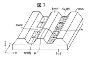
このように構成された隔壁BNKは、Y方向の隔壁BNKYの高さZ2をX方向の隔壁BNKXの高さZ1よりも高くして形成したことにより、図6に斜視図で示したようにY方向の隔壁BNKYに沿って配列された画素形成領域TER内に図7に示すように同じ色を発光する有機材料溶液、例えば赤色発光有機材料溶液OLERをこの画素形成領域TERの内容積VR1=VR2=・・・VRnに応じた溶液濃度の溶液量を矢印A方向にライン状に滴下して塗布した後、この有機材料溶液OLERを乾燥させることによってX方向の隔壁BNKX上の有機材料溶液OLERは撥水作用により弾かれて図8に斜視図で示すようにY方向の各画素形成領域TER内に均質な赤色発光有機発光層OLE(R)が形成される。 The partition wall BNK configured in this way is formed such that the height Z2 of the partition wall BNKY in the Y direction is higher than the height Z1 of the partition wall BNNKX in the X direction, and as shown in a perspective view in FIG. As shown in FIG. 7, an organic material solution that emits the same color, for example, a red light-emitting organic material solution OLE, is placed in the pixel formation region TER arranged along the partition wall BNKY in the direction, and the internal volume VR1 = VR2 of the pixel formation region TER. = ... After the amount of solution having a solution concentration corresponding to VRn is dropped and applied in a line in the direction of arrow A, the organic material solution OLER on the partition wall BNKX in the X direction is obtained by drying the organic material solution OLER. Repelled by the water repellent action, a homogeneous red light emitting organic light emitting layer OLE (R) is formed in each pixel forming region TER in the Y direction as shown in a perspective view in FIG.
また、図7に示すように赤色発光有機発光層OLE(R)に隔壁BNKを介して隣接する青色用画素形成領域TERBに青色発光有機材料溶液をその内容積VB1=VB2=・・・VBnに応じた溶液濃度の溶液量をライン状に滴下して塗布した後、この青色発光有機材料溶液を乾燥させることによってX方向の隔壁BNKX上の青色発光有機材料溶液は撥水作用により弾かれてY方向の各画素形成領域TERB内に均質な青色発光有機発光層を形成することができる。 Further, as shown in FIG. 7, the blue light emitting organic material solution is applied to the blue pixel forming region TERB adjacent to the red light emitting organic light emitting layer OLE (R) via the partition wall BNK so that the inner volume VB1 = VB2 =... VBn. After the solution amount of the corresponding solution concentration is dropped in a line shape and applied, the blue light emitting organic material solution on the X-direction partition wall BNKX is repelled by the water repellent action by drying this blue light emitting organic material solution. A uniform blue light emitting organic light emitting layer can be formed in each pixel forming region TERB in the direction.
つまり、本実施例では、隔壁BNKは異色画素と隣接する隔壁BNKYの高さよりも同色画素と隣接する隔壁BNKXの高さを低くしている。現行では、隔壁の高さを均一の高さにすることではなく、また、同色画素と隣接する隔壁の高さをゼロとすることではなく、異色画素と隣接する隔壁の高さより低く、ゼロよりも高くしている。具体的には、塗布された有機材料溶液が異色画素へ濡れ広がらない高い隔壁と、塗布された有機材料溶液が濡れ広がっても良いが、画素端部でリーク電流が発生しない程度の厚さを備えた低い隔壁と組み合せることにより、混色の発生を抑制している。 In other words, in this embodiment, the height of the partition wall BNKX adjacent to the same color pixel is lower than that of the partition wall BNKY adjacent to the different color pixel. At present, the height of the partition wall is not made uniform, and the height of the partition wall adjacent to the same color pixel is not set to zero, but is lower than the height of the partition wall adjacent to the different color pixel. Is also high. Specifically, the applied organic material solution may have a high partition wall that does not wet and spread to different color pixels, and the applied organic material solution may wet and spread, but the thickness is such that leakage current does not occur at the pixel edge. By combining with the low partition provided, the occurrence of color mixing is suppressed.
したがって、Y方向の隔壁BNKYの高さがX方向の隔壁BNKXよりも高く形成されているので、図7に示すように赤色発光有機材料溶液OLERがY方向の隔壁BNKYを矢印Bで示す方向に乗り越えて隣接する異色画素形成領域、例えば青色画素形成領域TERB内に濡れ広がることを抑止できるので、異色発光有機層を混色させることはない。また、隣接する異色発光の有機材料溶液についても全く同様である。 Therefore, since the height of the partition wall BNKY in the Y direction is higher than that of the partition wall BNKX in the X direction, the red light-emitting organic material solution OLE moves the partition wall BNKY in the Y direction in the direction indicated by the arrow B as shown in FIG. Since it is possible to suppress wetting and spreading in the different color pixel formation region, for example, the blue pixel formation region TERB, overcoming the different color light emitting organic layer, the color of the different color light emitting organic layer is not mixed. The same applies to the adjacent organic material solution of different color emission.
現行では、高分子系有機発光層を作製しているインクジェット法は、隔壁内に一定量の有機材料溶液を滴下しているが、溶液射出量や溶液滴下位置のバラツキ及びインク混色などの問題が生じていることから、容易なプロセスとは言い難い。また、画像表示装置の高解像度化に伴い、上記問題はより困難なプロセスが強いられる。これに対して本実施例では、同色画素間の隔壁BNKXの高さZ1が異色画素間の隔壁BNKYの高さZ2よりも低く形成することにより、Y方向の隔壁BNKY間に同一濃度の有機材料溶液SOLを滴下し、隔壁内容積に応じた溶液量を塗布(注入)することによって成膜することができるので、簡単で且つ容易なプロセスで均質な有機発光層の形成が可能となる。また、容易なプロセスにより高解像度化が容易に実現できる。 At present, the ink jet method for producing a polymer-based organic light emitting layer drops a certain amount of organic material solution in the partition wall, but there are problems such as variation in the amount of solution injection, dispersion of the solution dropping position, and ink color mixing. It is difficult to say that it is an easy process. Further, as the resolution of the image display device is increased, the above problem is forced to be a more difficult process. On the other hand, in the present embodiment, the height Z1 of the partition BNKYX between pixels of the same color is formed lower than the height Z2 of the partition BNKY between pixels of different colors, so that the organic material having the same concentration between the partitions BNKY in the Y direction. Since a film can be formed by dropping the solution SOL and applying (injecting) a solution amount corresponding to the inner volume of the partition wall, it is possible to form a homogeneous organic light emitting layer by a simple and easy process. Further, high resolution can be easily realized by an easy process.
次に、上記実施例1の構成において、画素形成領域TER内に有機発光層を形成する方法について説明する。まず、薄膜トランジスタTFTを形成した透光性メイン基板SUB1の画素電極である陽極上にホール注入層としてPEDT(ポリエチレンジオキシチヨフェン)/PSS(ポリスチレンスルホン酸)を約40nmの厚さに成膜した後、各色の発光層として、青色発光層は、F8(ポリジオクチルフルオレン)を約45nmの厚さに成膜した。また、緑色発光層は、PPV(ポリフェニレンビニレン)を約30nm,F8を約45nmの厚さに積層して成膜した。 Next, a method for forming an organic light emitting layer in the pixel formation region TER in the configuration of the first embodiment will be described. First, PEDT (polyethylene dioxythiophene) / PSS (polystyrene sulfonic acid) was formed in a thickness of about 40 nm as a hole injection layer on the anode which is the pixel electrode of the translucent main substrate SUB1 on which the thin film transistor TFT was formed. Thereafter, as the light emitting layer of each color, the blue light emitting layer was formed by depositing F8 (polydioctylfluorene) to a thickness of about 45 nm. The green light emitting layer was formed by laminating PPV (polyphenylene vinylene) to a thickness of about 30 nm and F8 to a thickness of about 45 nm.
さらに、赤色発光層は、R-PPVを約40nm,F8を約45nmの厚さに積層して成膜した。その後、LiF(フッ化リチウム)を約2nmの厚さに成膜した。さらに陰極材料としてCa(カルシウム)を約100nm,Al(アルミニウム)を約200nmの厚さに積層して成膜した。最後にSiN(窒化シリコン)を約50nm厚さで3層積層した。このようにして形成された有機発光素子に陽極と陰極との間に直流電圧約6Vを印加すると、輝度が約800cd/m2以上の白色発光を得ることができた。 Further, the red light emitting layer was formed by laminating R-PPV to a thickness of about 40 nm and F8 to a thickness of about 45 nm. Thereafter, LiF (lithium fluoride) was deposited to a thickness of about 2 nm. Furthermore, as a cathode material, Ca (calcium) was laminated to a thickness of about 100 nm and Al (aluminum) was laminated to a thickness of about 200 nm. Finally, three layers of SiN (silicon nitride) were laminated to a thickness of about 50 nm. When a DC voltage of about 6 V was applied between the anode and the cathode to the organic light emitting device thus formed, white light emission with a luminance of about 800 cd / m 2 or more could be obtained.
また、上記実施例1の構成において、画素形成領域TER内に有機発光層を形成する他の方法について説明する。まず、薄膜トランジスタTFTを形成した透光性メイン基板SUB1の画素電極である陽極上にホール注入層としてPEDT(ポリエチレンジオキシチヨフェン)/PSS(ポリスチレンスルホン酸)を約40nmの厚さに成膜した後、各色の発光層として、青色発光層は、F8(ポリジオクチルフルオレン)を約45nmの厚さに成膜した。また、緑色発光層は、PPV(ポリフェニレンビニレン)を約30nm,F8を約45nmの厚さに積層して成膜した。 In addition, another method for forming an organic light emitting layer in the pixel formation region TER in the configuration of the first embodiment will be described. First, PEDT (polyethylene dioxythiophene) / PSS (polystyrene sulfonic acid) was formed in a thickness of about 40 nm as a hole injection layer on the anode which is the pixel electrode of the translucent main substrate SUB1 on which the thin film transistor TFT was formed. Thereafter, as the light emitting layer of each color, the blue light emitting layer was formed by depositing F8 (polydioctylfluorene) to a thickness of about 45 nm. The green light emitting layer was formed by laminating PPV (polyphenylene vinylene) to a thickness of about 30 nm and F8 to a thickness of about 45 nm.
さらに、赤色発光層は、R-PPVを約40nm,F8を約45nmの厚さに積層して成膜した。その後、LiFを約2nmの厚さに成膜した。陰極材料としてCa/Alを約5nmの厚さに積層して成膜した。最後にSiNを約50nm厚さで3層積層した。このようにして形成された有機発光素子に陽極と陰極との間に直流電圧約6Vを印加すると、輝度が約800cd/m2以上の白色発光を得ることができた。 Further, the red light emitting layer was formed by laminating R-PPV to a thickness of about 40 nm and F8 to a thickness of about 45 nm. Thereafter, LiF was deposited to a thickness of about 2 nm. As a cathode material, Ca / Al was laminated to a thickness of about 5 nm to form a film. Finally, three layers of SiN having a thickness of about 50 nm were stacked. When a DC voltage of about 6 V was applied between the anode and the cathode to the organic light emitting device thus formed, white light emission with a luminance of about 800 cd / m 2 or more could be obtained.
また、上記実施例1の構成において、画素形成領域TER内に有機発光層を形成するさらに他の方法について説明する。まず、薄膜トランジスタTFTを形成した透光性メイン基板SUB1の画素電極である陽極上にホール注入層としてMTDATA(4,4’4”-トリス[-N-(-3-メチルフェニル)-N-フェニルアミド]トリフェニルアミン)を約70nm,α-NPDを約10nm,ジスチリルベンゼン誘導体(DTVBi)/ペリレンを約60nm(5%),トリス(8-ヒドロキシキノリノ)アルミニウム(Alq)を約60nmの厚さに順次成膜した。 Further, another method for forming an organic light emitting layer in the pixel formation region TER in the configuration of the first embodiment will be described. First, MTDATA (4,4'4 "-tris [-N-(-3-methylphenyl) -N-phenyl] is used as a hole injection layer on the anode which is the pixel electrode of the translucent main substrate SUB1 on which the thin film transistor TFT is formed. Amido] triphenylamine) about 70 nm, α-NPD about 10 nm, distyrylbenzene derivative (DTVBi) / perylene about 60 nm (5%), tris (8-hydroxyquinolino) aluminum (Alq) about 60 nm Films were sequentially formed in thickness.
その後、緑色発光層は、MTDATAを約70nm,α-NPDを約10nm,Alq/キナクドリンを約60nm(5%),Alqを約60nmの厚さにそれぞれ積層して成膜した。また、赤色発光層は、MTDATAを約70nm,α-NPDを約10nm,Alq/DCM2を約60nm(2%),Alqを約60nmの厚さに順次成膜した。最後に陰極材料としてAlを約70nm形成し、約50nmのSiN(窒化シリコン)を3層積層形成した。このようにして形成された有機発光素子に陽極と陰極との間に直流電圧約6Vを印加すると、輝度が約800cd/m2以上の白色発光を得ることができた。 Thereafter, the green light emitting layer was formed by laminating MTDATA to a thickness of about 70 nm, α-NPD to a thickness of about 10 nm, Alq / quinacdrine to a thickness of about 60 nm (5%), and Alq to a thickness of about 60 nm. In addition, the red light emitting layer was sequentially formed to a thickness of about 70 nm for MTDATA, about 10 nm for α-NPD, about 60 nm (2%) for Alq / DCM2, and about 60 nm for Alq. Finally, about 70 nm of Al was formed as the cathode material, and three layers of about 50 nm of SiN (silicon nitride) were stacked. When a DC voltage of about 6 V was applied between the anode and the cathode to the organic light emitting device thus formed, white light emission with a luminance of about 800 cd / m 2 or more could be obtained.
次に、上記実施例1の構成において、画素形成領域TER内に有機発光層を形成する他の方法について説明する。まず、薄膜トランジスタTFTを形成した透光性メイン基板SUB1の画素電極である陽極上にホール注入層としてMTDATAを約70nm,α-NPDを約10nm,ジスチリルベンゼン誘導体(DTVBi)/ペリレンを約60nm(5%),トリス(8-ヒドロキシキノリノ)アルミニウム(Alq)を約60nmの厚さに順次成膜した。 Next, another method for forming an organic light emitting layer in the pixel formation region TER in the configuration of the first embodiment will be described. First, MTDATA is about 70 nm, α-NPD is about 10 nm, distyrylbenzene derivative (DTVBi) / perylene is about 60 nm as a hole injection layer on the anode which is a pixel electrode of the translucent main substrate SUB1 on which the thin film transistor TFT is formed. 5%) and tris (8-hydroxyquinolino) aluminum (Alq) were sequentially formed to a thickness of about 60 nm.
その後、緑色発光層は、MTDATAを約70nm,α-NPDを約10nm,Alq/キナクドリンを約60nm(5%),Alqを約60nmの厚さにそれぞれ積層して成膜した。また、赤色発光層は、MTDATAを約70nm,α-NPDを約10nm,Alq/DCM2を約60nm(2%),Alqを約60nmの厚さに順次成膜した。最後に陰極材料としてLiFを約0.5nm,Mg/Agを約5nm形成し、約50nmのSiNを3層積層形成した。このようにして形成された有機発光素子に陽極と陰極との間に直流電圧約6Vを印加すると、輝度が約800cd/m2以上の白色発光を得ることができた。 Thereafter, the green light emitting layer was formed by laminating MTDATA to a thickness of about 70 nm, α-NPD to a thickness of about 10 nm, Alq / quinacdrine to a thickness of about 60 nm (5%), and Alq to a thickness of about 60 nm. In addition, the red light emitting layer was sequentially formed to a thickness of about 70 nm for MTDATA, about 10 nm for α-NPD, about 60 nm (2%) for Alq / DCM2, and about 60 nm for Alq. Finally, about 0.5 nm of LiF and about 5 nm of Mg / Ag were formed as cathode materials, and three layers of SiN of about 50 nm were laminated. When a DC voltage of about 6 V was applied between the anode and the cathode to the organic light emitting device thus formed, white light emission with a luminance of about 800 cd / m 2 or more could be obtained.
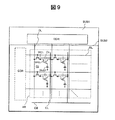
図9は、有機発光表示装置の全体構成例の説明図である。図1で説明した構成を有する画素(PX)をマトリクス状に配置して2次元の有機発光表示装置を構成している。各画素(PX)は、第1の薄膜トランジスタTFT1と、第2の薄膜トランジスタTFT2と、コンデンサCsと、有機発光素子OLEDとから構成される。有機発光素子OLEDは、図1で説明した構造の画素を構成する。表示領域AR内には、各画素に駆動信号を供給するためのドレイン線DLとゲート線GLとが交差配置されている。メイン基板SUB1の一部は封止ガラス基板SUB2よりサイズが大きく、封止ガラス基板SUB2からはみ出している。このはみ出し部分にドレインドライバDDRが搭載され、ドレイン線DLに表示信号を供給する。 FIG. 9 is an explanatory diagram of an example of the overall configuration of the organic light emitting display device. A pixel (PX) having the configuration described with reference to FIG. 1 is arranged in a matrix to form a two-dimensional organic light emitting display device. Each pixel (PX) includes a first thin film transistor TFT1, a second thin film transistor TFT2, a capacitor Cs, and an organic light emitting element OLED. The organic light emitting element OLED constitutes a pixel having the structure described in FIG. In the display area AR, a drain line DL and a gate line GL for supplying a drive signal to each pixel are arranged in an intersecting manner. A part of the main substrate SUB1 is larger in size than the sealing glass substrate SUB2 and protrudes from the sealing glass substrate SUB2. A drain driver DDR is mounted on the protruding portion and supplies a display signal to the drain line DL.
一方、ゲートドライバGDRは、封止ガラス基板SUB2で覆われるメイン基板SUB1上に所謂システム・オン・グラスと称する形態で直接形成されている。このゲートドライバGDRにゲート線GLが接続されている。なお、表示領域ARには電源線CLが配置されている。この電源線CLは電源線バス線を介して図示しない端子で外部電源に接続されている。 On the other hand, the gate driver GDR is directly formed on the main substrate SUB1 covered with the sealing glass substrate SUB2 in the form of so-called system-on-glass. A gate line GL is connected to the gate driver GDR. A power line CL is arranged in the display area AR. The power supply line CL is connected to an external power supply at a terminal (not shown) through a power supply line bus line.
ゲート線GLは、画素PXを構成する第1の薄膜トランジスタTFT1のソース・ドレイン電極の一方(ここではゲート電極)に接続し、ドレイン線DLはソース・ドレイン電極の一方(ここではソース電極)に接続されている。この第1の薄膜トランジスタTFT1は、画素PXに表示信号を取り込むためのスイッチであり、ゲート線GLで選択されてオンとなったときドレイン線DLから供給される表示信号に応じた電荷を容量Csに蓄積する。第2の薄膜トランジスタTFT2は、第1の薄膜トランジスタTFT1がオフした時点でオンとなり、容量Csに蓄積された表示信号の大きさに応じた電流を電源線CLから有機発光素子OLEDに供給する。有機発光素子OLEDは供給された電流量に応じて発光する。 The gate line GL is connected to one of the source / drain electrodes (here, the gate electrode) of the first thin film transistor TFT1 constituting the pixel PX, and the drain line DL is connected to one of the source / drain electrodes (here, the source electrode). Has been. The first thin film transistor TFT1 is a switch for taking a display signal into the pixel PX, and when it is selected by the gate line GL and turned on, a charge corresponding to the display signal supplied from the drain line DL is supplied to the capacitor Cs. accumulate. The second thin film transistor TFT2 is turned on when the first thin film transistor TFT1 is turned off, and supplies a current corresponding to the magnitude of the display signal stored in the capacitor Cs from the power supply line CL to the organic light emitting element OLED. The organic light emitting element OLED emits light according to the supplied current amount.
なお、前述した実施例においては、ボトムエミッション型の有機発光表示装置について説明したが、本発明はこれに限定されるものではなく、トップエミッション型の有機発光表示装置に適用しても、前述した各実施例と同様の作用効果が得られることは勿論である。 In the above-described embodiments, the bottom emission type organic light emitting display device has been described. However, the present invention is not limited to this, and the present invention may be applied to a top emission type organic light emitting display device. Needless to say, the same effects as those of the respective embodiments can be obtained.
また、前述した実施例においては、画像表示装置として有機発光素子を搭載する有機発光表示装置について説明したが、本発明はこれに限定されるものではなく、有機発光素子を搭載したTV,PCモニタ,ノート型PC,PDA,携帯電話器,デジタルスチルカメラ,デジタルビデオカメラまたはカーナビ用モニタ等の全般に適用できることは言うまでもない。 Further, in the above-described embodiments, the organic light emitting display device in which the organic light emitting element is mounted as the image display device has been described. However, the present invention is not limited to this, and the TV and PC monitor in which the organic light emitting element is mounted. Needless to say, the present invention can be applied to notebook computers, PDAs, mobile phones, digital still cameras, digital video cameras, car navigation monitors, and the like.
SUB・・・メイン基板(透光性基板)、SUB1・・・メイン基板(透光性基板)、SUB2・・・封止ガラス基板(絶縁性基板)、TFT・・・薄膜トランジスタ、AD・・・陽極(第1の電極)、CD・・・陰極(第2の電極)、OLE・・・有機発光層、OLE(R)・・・赤色有機発光層、OLE(G)・・・緑色有機発光層、OLE(B)・・・青色有機発光層、OLED・・・有機発光素子、PSI・・・ポリシリコン半導体層、IL・・・層間絶縁膜、DL・・・データ信号配線、PL・・・電源配線、PSV・・・パッシベーション層、L・・・発光光、BNK・・・隔壁(バンク)、BNKX・・・X方向の隔壁、BNKY・・・Y方向の隔壁、SOL・・・有機材料溶液、TER・・・画素形成領域。
SUB ... main substrate (translucent substrate), SUB1 ... main substrate (translucent substrate), SUB2 ... sealing glass substrate (insulating substrate), TFT ... thin film transistor, AD ... Anode (first electrode), CD ... cathode (second electrode), OLE ... organic light emitting layer, OLE (R) ... red organic light emitting layer, OLE (G) ... green organic light emitting Layer, OLE (B) ... blue organic light emitting layer, OLED ... organic light emitting element, PSI ... polysilicon semiconductor layer, IL ... interlayer insulating film, DL ... data signal wiring, PL ...・ Power supply wiring, PSV: Passivation layer, L: Emission light, BNK: Partition wall (bank), BNKX: Partition in X direction, BNKY: Partition in Y direction, SOL: Organic Material solution, TER: Pixel formation region.
Claims (8)
前記発光層は、当該発光層の発光によりストライプ状の同色画素が並んで設置され、前記同色画素間の前記隔壁の高さが異色画素間の前記隔壁に高さよりも低いことを特徴とする画像表示装置。 A plurality of light-emitting elements are provided in a main surface of a light-transmitting substrate that is hermetically sealed with a sealing member interposed at a peripheral portion so as to face the insulating substrate, and each of the light-emitting elements is the light-transmitting substrate. A plurality of first electrodes formed on the main surface of the substrate, a light emitting layer formed to cover the plurality of first electrodes and having a light emitting ability, and common to the plurality of light emitting elements on the light emitting layer And the plurality of light emitting elements form pixels that are partitioned by partition walls, and emit light from the light emitting layer through the first electrode. An image display device that emits light to a substrate side,
The light emitting layer is configured such that stripe-shaped same color pixels are arranged side by side by light emission of the light emitting layer, and the height of the partition walls between the same color pixels is lower than the height of the partition walls between different color pixels. Display device.
The image display device according to claim 1, wherein the light emitting layer is an inorganic light emitting layer formed by a vapor deposition method.
Priority Applications (2)
| Application Number | Priority Date | Filing Date | Title |
|---|---|---|---|
| JP2006050624A JP2007234232A (en) | 2006-02-27 | 2006-02-27 | Image display device |
| US11/678,726 US20070200488A1 (en) | 2006-02-27 | 2007-02-26 | Display device |
Applications Claiming Priority (1)
| Application Number | Priority Date | Filing Date | Title |
|---|---|---|---|
| JP2006050624A JP2007234232A (en) | 2006-02-27 | 2006-02-27 | Image display device |
Publications (2)
| Publication Number | Publication Date |
|---|---|
| JP2007234232A true JP2007234232A (en) | 2007-09-13 |
| JP2007234232A5 JP2007234232A5 (en) | 2009-04-16 |
Family
ID=38443332
Family Applications (1)
| Application Number | Title | Priority Date | Filing Date |
|---|---|---|---|
| JP2006050624A Pending JP2007234232A (en) | 2006-02-27 | 2006-02-27 | Image display device |
Country Status (2)
| Country | Link |
|---|---|
| US (1) | US20070200488A1 (en) |
| JP (1) | JP2007234232A (en) |
Cited By (19)
| Publication number | Priority date | Publication date | Assignee | Title |
|---|---|---|---|---|
| JP2009070859A (en) * | 2007-09-10 | 2009-04-02 | Casio Comput Co Ltd | Organic electroluminescence display and its fabrication process |
| JP2009086155A (en) * | 2007-09-28 | 2009-04-23 | Toppan Printing Co Ltd | Image forming apparatus |
| JP2009146848A (en) * | 2007-12-18 | 2009-07-02 | Seiko Epson Corp | Light-emitting device, and electronic apparatus |
| JP2010114058A (en) * | 2008-11-10 | 2010-05-20 | Samsung Mobile Display Co Ltd | Organic electroluminescent display device, and method of manufacturing the same |
| JP2011108578A (en) * | 2009-11-20 | 2011-06-02 | Toppan Printing Co Ltd | Organic el light emitting element and method of manufacturing the same |
| WO2011105329A1 (en) * | 2010-02-25 | 2011-09-01 | 住友化学株式会社 | Manufacturing method for light-emitting devices |
| JP2011191730A (en) * | 2009-09-08 | 2011-09-29 | Ricoh Co Ltd | Display device, manufacturing method thereof, and electronic equipment |
| JP2014103112A (en) * | 2012-11-20 | 2014-06-05 | Regents Of Univ Of Michigan:The | Optoelectronic device manufactured by controlling vapor-phase flow |
| US8902140B2 (en) | 2008-11-11 | 2014-12-02 | Sharp Kabushiki Kaisha | Color conversion filter panel for color organic electroluminescent display and color organic electroluminescent display |
| US9640592B2 (en) | 2014-04-30 | 2017-05-02 | Joled Inc. | Method for forming functional layer of organic light-emitting device and method for manufacturing organic light-emitting device |
| WO2017208660A1 (en) * | 2016-05-30 | 2017-12-07 | 株式会社Joled | Display device and electronic device |
| US9997575B2 (en) | 2014-04-08 | 2018-06-12 | Joled Inc. | Organic light emitting device and method for manufacturing same |
| KR20190005953A (en) * | 2016-06-15 | 2019-01-16 | 가부시키가이샤 제이올레드 | Display and electronic devices |
| WO2020065937A1 (en) * | 2018-09-28 | 2020-04-02 | シャープ株式会社 | Display device |
| US10644085B2 (en) | 2017-08-28 | 2020-05-05 | Joled Inc. | Self-luminous display panel manufacturing method and self-luminous display panel |
| KR20200056912A (en) | 2018-11-15 | 2020-05-25 | 가부시키가이샤 제이올레드 | Organic el display panel manufacturing method and functional layer forming device |
| US10714549B2 (en) | 2018-02-23 | 2020-07-14 | Joled Inc. | Organic EL display panel manufacturing method and organic EL display panel |
| US10861910B2 (en) | 2017-09-08 | 2020-12-08 | Joled Inc. | Organic EL display panel and method for manufacturing organic EL display panel |
| US11108029B2 (en) | 2018-11-15 | 2021-08-31 | Joled Inc. | Organic EL display panel manufacturing method and functional layer forming device |
Families Citing this family (20)
| Publication number | Priority date | Publication date | Assignee | Title |
|---|---|---|---|---|
| KR101037037B1 (en) * | 2008-05-29 | 2011-05-25 | 파나소닉 주식회사 | Organic EL display and manufacturing method thereof |
| KR101254748B1 (en) | 2009-05-06 | 2013-04-15 | 엘지디스플레이 주식회사 | Organic Light Emitting Display Device and Manufacturing Method of the same |
| KR101653844B1 (en) * | 2010-04-19 | 2016-09-02 | 가부시키가이샤 제이올레드 | Organic el display panel and oraganic el display apparatus having the same and method of manufacturing organic el display panel |
| DE102010042727A1 (en) * | 2010-10-21 | 2012-05-10 | Ledon Oled Lighting Gmbh & Co. Kg | OLED module |
| TWI511281B (en) * | 2013-06-11 | 2015-12-01 | Ye Xin Technology Consulting Co Ltd | Oled panel |
| US10910350B2 (en) * | 2014-05-24 | 2021-02-02 | Hiphoton Co., Ltd. | Structure of a semiconductor array |
| KR102525051B1 (en) * | 2015-01-30 | 2023-04-25 | 삼성디스플레이 주식회사 | Organic light-emitting display |
| KR102466686B1 (en) * | 2015-04-15 | 2022-11-14 | 삼성디스플레이 주식회사 | Light emitting display device |
| KR102457536B1 (en) * | 2015-06-30 | 2022-10-21 | 엘지디스플레이 주식회사 | Organic light emitting display device |
| JP6685675B2 (en) | 2015-09-07 | 2020-04-22 | 株式会社Joled | Organic EL device, organic EL display panel using the same, and method for manufacturing organic EL display panel |
| CN109801939B (en) * | 2017-11-17 | 2021-11-16 | 京东方科技集团股份有限公司 | Display substrate, manufacturing method thereof and display device |
| CN109285865A (en) | 2018-09-17 | 2019-01-29 | 京东方科技集团股份有限公司 | A kind of display base plate and its manufacturing method, display device |
| CN111403432B (en) * | 2018-12-31 | 2023-11-03 | 乐金显示有限公司 | Organic light emitting display device and method of manufacturing the same |
| KR20210086170A (en) * | 2019-12-31 | 2021-07-08 | 엘지디스플레이 주식회사 | Organic light emitting display device |
| CN111710694B (en) * | 2020-05-28 | 2022-10-25 | 京东方科技集团股份有限公司 | Display substrate, manufacturing method thereof and display device |
| CN111584605B (en) * | 2020-05-29 | 2023-04-07 | 京东方科技集团股份有限公司 | Array substrate, preparation method, display panel and display device |
| CN112234085B (en) * | 2020-10-15 | 2022-07-08 | 京东方科技集团股份有限公司 | Array substrate and manufacturing method thereof, display panel and display device |
| CN113270461B (en) * | 2021-05-19 | 2022-11-25 | 京东方科技集团股份有限公司 | Display substrate, manufacturing method thereof and display device |
| WO2023092436A1 (en) * | 2021-11-26 | 2023-06-01 | 京东方科技集团股份有限公司 | Display panel, display device, and method for manufacturing display panel |
| CN116828916A (en) * | 2022-03-21 | 2023-09-29 | 京东方科技集团股份有限公司 | Display substrate, preparation method thereof and display device |
Citations (4)
| Publication number | Priority date | Publication date | Assignee | Title |
|---|---|---|---|---|
| JP2005310713A (en) * | 2004-04-26 | 2005-11-04 | Seiko Epson Corp | Organic el device, its manufacturing method and electronic apparatus |
| WO2006054421A1 (en) * | 2004-10-28 | 2006-05-26 | Sharp Kabushiki Kaisha | Organic electroluminescence panel and production method therefor, and color filter substrate and production method therefore |
| JP2007095521A (en) * | 2005-09-29 | 2007-04-12 | Toppan Printing Co Ltd | Manufacturing method of organic electroluminescent element |
| JP2007188862A (en) * | 2005-12-13 | 2007-07-26 | Canon Inc | Organic el light-emitting device and its manufacturing method |
Family Cites Families (9)
| Publication number | Priority date | Publication date | Assignee | Title |
|---|---|---|---|---|
| JP2003229256A (en) * | 2002-02-04 | 2003-08-15 | Seiko Epson Corp | Manufacturing method of organic el device, and ink component for organic el device |
| US7190335B2 (en) * | 2002-03-26 | 2007-03-13 | Semiconductor Energy Laboratory Co., Ltd. | Light emitting device and method of manufacturing the same |
| KR100508002B1 (en) * | 2002-09-03 | 2005-08-17 | 엘지.필립스 엘시디 주식회사 | fabrication method of an organic electro-luminescence device using nozzle coating |
| KR100528910B1 (en) * | 2003-01-22 | 2005-11-15 | 삼성에스디아이 주식회사 | Polymer organic light emitting diode |
| JP4538649B2 (en) * | 2003-08-28 | 2010-09-08 | 奇美電子股▲ふん▼有限公司 | Organic EL display that eliminates uneven brightness and manufacturing method thereof |
| US7816863B2 (en) * | 2003-09-12 | 2010-10-19 | Semiconductor Energy Laboratory Co., Ltd. | Light emitting device and method for manufacturing the same |
| ATE383733T1 (en) * | 2003-11-18 | 2008-01-15 | 3M Innovative Properties Co | ELECTROLUMINESCENT COMPONENTS AND METHOD FOR PRODUCING ELECTROLUMINESCENT COMPONENTS HAVING A COLOR CONVERSION ELEMENT |
| US20050153114A1 (en) * | 2004-01-14 | 2005-07-14 | Rahul Gupta | Printing of organic electronic devices |
| US7358526B2 (en) * | 2005-09-28 | 2008-04-15 | Osram Opto Semiconductors Gmbh | OLED separating structures |
-
2006
- 2006-02-27 JP JP2006050624A patent/JP2007234232A/en active Pending
-
2007
- 2007-02-26 US US11/678,726 patent/US20070200488A1/en not_active Abandoned
Patent Citations (4)
| Publication number | Priority date | Publication date | Assignee | Title |
|---|---|---|---|---|
| JP2005310713A (en) * | 2004-04-26 | 2005-11-04 | Seiko Epson Corp | Organic el device, its manufacturing method and electronic apparatus |
| WO2006054421A1 (en) * | 2004-10-28 | 2006-05-26 | Sharp Kabushiki Kaisha | Organic electroluminescence panel and production method therefor, and color filter substrate and production method therefore |
| JP2007095521A (en) * | 2005-09-29 | 2007-04-12 | Toppan Printing Co Ltd | Manufacturing method of organic electroluminescent element |
| JP2007188862A (en) * | 2005-12-13 | 2007-07-26 | Canon Inc | Organic el light-emitting device and its manufacturing method |
Cited By (27)
| Publication number | Priority date | Publication date | Assignee | Title |
|---|---|---|---|---|
| JP2009070859A (en) * | 2007-09-10 | 2009-04-02 | Casio Comput Co Ltd | Organic electroluminescence display and its fabrication process |
| JP2009086155A (en) * | 2007-09-28 | 2009-04-23 | Toppan Printing Co Ltd | Image forming apparatus |
| JP2009146848A (en) * | 2007-12-18 | 2009-07-02 | Seiko Epson Corp | Light-emitting device, and electronic apparatus |
| US8599113B2 (en) | 2008-11-10 | 2013-12-03 | Samsung Display Co., Ltd. | Organic light emitting display device and method of manufacturing the same |
| JP2010114058A (en) * | 2008-11-10 | 2010-05-20 | Samsung Mobile Display Co Ltd | Organic electroluminescent display device, and method of manufacturing the same |
| US8902140B2 (en) | 2008-11-11 | 2014-12-02 | Sharp Kabushiki Kaisha | Color conversion filter panel for color organic electroluminescent display and color organic electroluminescent display |
| JP2011191730A (en) * | 2009-09-08 | 2011-09-29 | Ricoh Co Ltd | Display device, manufacturing method thereof, and electronic equipment |
| JP2011108578A (en) * | 2009-11-20 | 2011-06-02 | Toppan Printing Co Ltd | Organic el light emitting element and method of manufacturing the same |
| JP2011175910A (en) * | 2010-02-25 | 2011-09-08 | Sumitomo Chemical Co Ltd | Method of manufacturing light-emitting device |
| WO2011105329A1 (en) * | 2010-02-25 | 2011-09-01 | 住友化学株式会社 | Manufacturing method for light-emitting devices |
| JP2014103112A (en) * | 2012-11-20 | 2014-06-05 | Regents Of Univ Of Michigan:The | Optoelectronic device manufactured by controlling vapor-phase flow |
| US10312308B2 (en) | 2014-04-08 | 2019-06-04 | Joled, Inc. | Organic light emitting device and method for manufacturing same |
| US9997575B2 (en) | 2014-04-08 | 2018-06-12 | Joled Inc. | Organic light emitting device and method for manufacturing same |
| US9640592B2 (en) | 2014-04-30 | 2017-05-02 | Joled Inc. | Method for forming functional layer of organic light-emitting device and method for manufacturing organic light-emitting device |
| WO2017208660A1 (en) * | 2016-05-30 | 2017-12-07 | 株式会社Joled | Display device and electronic device |
| CN109315048A (en) * | 2016-05-30 | 2019-02-05 | 株式会社日本有机雷特显示器 | Display device and electronic equipment |
| JPWO2017208660A1 (en) * | 2016-05-30 | 2018-08-02 | 株式会社Joled | Display device and electronic device |
| CN109315048B (en) * | 2016-05-30 | 2022-06-10 | 株式会社日本有机雷特显示器 | Display device and electronic apparatus |
| US11404501B2 (en) | 2016-05-30 | 2022-08-02 | Joled Inc. | Display unit and electronic apparatus |
| KR20190005953A (en) * | 2016-06-15 | 2019-01-16 | 가부시키가이샤 제이올레드 | Display and electronic devices |
| KR102248489B1 (en) | 2016-06-15 | 2021-05-06 | 가부시키가이샤 제이올레드 | Display devices and electronic devices |
| US10644085B2 (en) | 2017-08-28 | 2020-05-05 | Joled Inc. | Self-luminous display panel manufacturing method and self-luminous display panel |
| US10861910B2 (en) | 2017-09-08 | 2020-12-08 | Joled Inc. | Organic EL display panel and method for manufacturing organic EL display panel |
| US10714549B2 (en) | 2018-02-23 | 2020-07-14 | Joled Inc. | Organic EL display panel manufacturing method and organic EL display panel |
| WO2020065937A1 (en) * | 2018-09-28 | 2020-04-02 | シャープ株式会社 | Display device |
| KR20200056912A (en) | 2018-11-15 | 2020-05-25 | 가부시키가이샤 제이올레드 | Organic el display panel manufacturing method and functional layer forming device |
| US11108029B2 (en) | 2018-11-15 | 2021-08-31 | Joled Inc. | Organic EL display panel manufacturing method and functional layer forming device |
Also Published As
| Publication number | Publication date |
|---|---|
| US20070200488A1 (en) | 2007-08-30 |
Similar Documents
| Publication | Publication Date | Title |
|---|---|---|
| JP2007234232A (en) | Image display device | |
| US11514857B2 (en) | Organic light emitting diode display | |
| US20220069057A1 (en) | Display device including a power supply line that overlaps a driving circuit | |
| US7629740B2 (en) | Display device with stacked layer body | |
| US9991321B2 (en) | Organic light emitting diode display device and method of fabricating the same | |
| US7535169B2 (en) | Organic electroluminescent device, method for producing the same, and electronic appliance | |
| US8691603B2 (en) | Organic el device manufacturing method, organic el device, and electronic apparatus having a luminescent layer disposed over another luminescent layer | |
| US9123665B2 (en) | Organic EL device, method for manufacturing the same, and electronic apparatus | |
| JP2010010670A (en) | Light emitting device and method of manufacturing the same | |
| US20100193778A1 (en) | Organic light emitting diode display and method of manufacturing the same | |
| US7294960B2 (en) | Organic electroluminescent device with HIL/HTL specific to each RGB pixel | |
| US8278137B2 (en) | Electroluminescent devices comprising bus bars | |
| US8847210B2 (en) | Organic light emitting diode display | |
| JP2012109138A (en) | Method for manufacturing organic el display device, organic el display device, and electronic apparatus | |
| KR101202547B1 (en) | Organic Electroluminescent Device and method for fabricating thereof | |
| JP4617951B2 (en) | LIGHT EMITTING DEVICE, ITS MANUFACTURING METHOD, AND ELECTRONIC DEVICE | |
| JP2007010761A (en) | Display device | |
| JP5761392B2 (en) | Method for manufacturing organic EL device and electronic device | |
| JP2012248449A (en) | Organic el device | |
| US11963415B2 (en) | Display device including a power supply line that overlaps a driving circuit | |
| JP2010040816A (en) | Organic el device, manufacturing method of the organic el device, and electronic apparatus | |
| KR20040085383A (en) | Organic electroluminescence device having multiple partition structures and fabricating method thereof | |
| JP2006100191A (en) | Display device, and manufacturing method of display device | |
| US20110171760A1 (en) | Method for manufacturing thin film transistor and display device | |
| KR20060077283A (en) | Organic electroluminescence display device and method for fabricating the same |
Legal Events
| Date | Code | Title | Description |
|---|---|---|---|
| A521 | Request for written amendment filed |
Free format text: JAPANESE INTERMEDIATE CODE: A523 Effective date: 20090226 |
|
| A621 | Written request for application examination |
Free format text: JAPANESE INTERMEDIATE CODE: A621 Effective date: 20090226 |
|
| A977 | Report on retrieval |
Free format text: JAPANESE INTERMEDIATE CODE: A971007 Effective date: 20101105 |
|
| A131 | Notification of reasons for refusal |
Free format text: JAPANESE INTERMEDIATE CODE: A131 Effective date: 20101207 |
|
| A521 | Request for written amendment filed |
Free format text: JAPANESE INTERMEDIATE CODE: A523 Effective date: 20110204 |
|
| A711 | Notification of change in applicant |
Free format text: JAPANESE INTERMEDIATE CODE: A712 Effective date: 20110218 |
|
| RD03 | Notification of appointment of power of attorney |
Free format text: JAPANESE INTERMEDIATE CODE: A7423 Effective date: 20110218 |
|
| A02 | Decision of refusal |
Free format text: JAPANESE INTERMEDIATE CODE: A02 Effective date: 20110621 |