JP2007010761A - Display device - Google Patents
Display device Download PDFInfo
- Publication number
- JP2007010761A JP2007010761A JP2005188427A JP2005188427A JP2007010761A JP 2007010761 A JP2007010761 A JP 2007010761A JP 2005188427 A JP2005188427 A JP 2005188427A JP 2005188427 A JP2005188427 A JP 2005188427A JP 2007010761 A JP2007010761 A JP 2007010761A
- Authority
- JP
- Japan
- Prior art keywords
- electrode
- display device
- light emitting
- substrate
- wall surfaces
- Prior art date
- Legal status (The legal status is an assumption and is not a legal conclusion. Google has not performed a legal analysis and makes no representation as to the accuracy of the status listed.)
- Granted
Links
- 238000005192 partition Methods 0.000 claims abstract description 48
- 239000000758 substrate Substances 0.000 claims abstract description 45
- 239000000463 material Substances 0.000 claims description 39
- 239000011248 coating agent Substances 0.000 claims 1
- 238000000576 coating method Methods 0.000 claims 1
- 238000007599 discharging Methods 0.000 claims 1
- 238000004519 manufacturing process Methods 0.000 abstract description 30
- 230000001681 protective effect Effects 0.000 abstract description 8
- 239000010410 layer Substances 0.000 description 52
- 238000000034 method Methods 0.000 description 30
- 238000007740 vapor deposition Methods 0.000 description 12
- 238000001771 vacuum deposition Methods 0.000 description 10
- 239000010408 film Substances 0.000 description 9
- 238000000059 patterning Methods 0.000 description 7
- 229920000642 polymer Polymers 0.000 description 7
- 239000011241 protective layer Substances 0.000 description 7
- 229910052782 aluminium Inorganic materials 0.000 description 5
- XAGFODPZIPBFFR-UHFFFAOYSA-N aluminium Chemical compound [Al] XAGFODPZIPBFFR-UHFFFAOYSA-N 0.000 description 5
- 239000002585 base Substances 0.000 description 5
- 239000007788 liquid Substances 0.000 description 5
- 239000011159 matrix material Substances 0.000 description 5
- 239000011368 organic material Substances 0.000 description 5
- 229910001316 Ag alloy Inorganic materials 0.000 description 4
- PCHJSUWPFVWCPO-UHFFFAOYSA-N gold Chemical compound [Au] PCHJSUWPFVWCPO-UHFFFAOYSA-N 0.000 description 4
- 229910052737 gold Inorganic materials 0.000 description 4
- 239000010931 gold Substances 0.000 description 4
- SJCKRGFTWFGHGZ-UHFFFAOYSA-N magnesium silver Chemical compound [Mg].[Ag] SJCKRGFTWFGHGZ-UHFFFAOYSA-N 0.000 description 4
- 230000008569 process Effects 0.000 description 4
- 239000010409 thin film Substances 0.000 description 4
- 230000000694 effects Effects 0.000 description 3
- 239000011521 glass Substances 0.000 description 3
- 238000007641 inkjet printing Methods 0.000 description 3
- 238000002955 isolation Methods 0.000 description 3
- 229920000553 poly(phenylenevinylene) Polymers 0.000 description 3
- 239000002861 polymer material Substances 0.000 description 3
- -1 polyphenylene vinylene Polymers 0.000 description 3
- 229910052814 silicon oxide Inorganic materials 0.000 description 3
- 239000000243 solution Substances 0.000 description 3
- IJGRMHOSHXDMSA-UHFFFAOYSA-N Atomic nitrogen Chemical compound N#N IJGRMHOSHXDMSA-UHFFFAOYSA-N 0.000 description 2
- 229910052581 Si3N4 Inorganic materials 0.000 description 2
- VYPSYNLAJGMNEJ-UHFFFAOYSA-N Silicium dioxide Chemical compound O=[Si]=O VYPSYNLAJGMNEJ-UHFFFAOYSA-N 0.000 description 2
- QVGXLLKOCUKJST-UHFFFAOYSA-N atomic oxygen Chemical compound [O] QVGXLLKOCUKJST-UHFFFAOYSA-N 0.000 description 2
- 230000015572 biosynthetic process Effects 0.000 description 2
- 229920001940 conductive polymer Polymers 0.000 description 2
- 238000010586 diagram Methods 0.000 description 2
- 238000001704 evaporation Methods 0.000 description 2
- 230000008020 evaporation Effects 0.000 description 2
- 229910052751 metal Inorganic materials 0.000 description 2
- 239000002184 metal Substances 0.000 description 2
- 150000002894 organic compounds Chemical class 0.000 description 2
- 239000001301 oxygen Substances 0.000 description 2
- 229910052760 oxygen Inorganic materials 0.000 description 2
- 238000000206 photolithography Methods 0.000 description 2
- 239000002985 plastic film Substances 0.000 description 2
- 229920006255 plastic film Polymers 0.000 description 2
- 229920001467 poly(styrenesulfonates) Polymers 0.000 description 2
- 229920001721 polyimide Polymers 0.000 description 2
- 239000009719 polyimide resin Substances 0.000 description 2
- HQVNEWCFYHHQES-UHFFFAOYSA-N silicon nitride Chemical compound N12[Si]34N5[Si]62N3[Si]51N64 HQVNEWCFYHHQES-UHFFFAOYSA-N 0.000 description 2
- XLYOFNOQVPJJNP-UHFFFAOYSA-N water Chemical compound O XLYOFNOQVPJJNP-UHFFFAOYSA-N 0.000 description 2
- YDENDYPVGDGGMZ-UHFFFAOYSA-N 2-(2-thiophen-2-ylethyl)thiophene Chemical compound C=1C=CSC=1CCC1=CC=CS1 YDENDYPVGDGGMZ-UHFFFAOYSA-N 0.000 description 1
- 229920001609 Poly(3,4-ethylenedioxythiophene) Polymers 0.000 description 1
- 239000004695 Polyether sulfone Substances 0.000 description 1
- 229910004205 SiNX Inorganic materials 0.000 description 1
- 239000000853 adhesive Substances 0.000 description 1
- 230000001070 adhesive effect Effects 0.000 description 1
- 229910052783 alkali metal Inorganic materials 0.000 description 1
- 150000001340 alkali metals Chemical class 0.000 description 1
- 229910052784 alkaline earth metal Inorganic materials 0.000 description 1
- 150000001342 alkaline earth metals Chemical class 0.000 description 1
- 229910052788 barium Inorganic materials 0.000 description 1
- 229910052790 beryllium Inorganic materials 0.000 description 1
- 230000000903 blocking effect Effects 0.000 description 1
- 229910052792 caesium Inorganic materials 0.000 description 1
- 229910052791 calcium Inorganic materials 0.000 description 1
- 239000003086 colorant Substances 0.000 description 1
- 238000000151 deposition Methods 0.000 description 1
- 230000008021 deposition Effects 0.000 description 1
- 239000002274 desiccant Substances 0.000 description 1
- 230000006866 deterioration Effects 0.000 description 1
- 150000004985 diamines Chemical class 0.000 description 1
- 239000007772 electrode material Substances 0.000 description 1
- 238000005401 electroluminescence Methods 0.000 description 1
- 230000005525 hole transport Effects 0.000 description 1
- AMGQUBHHOARCQH-UHFFFAOYSA-N indium;oxotin Chemical compound [In].[Sn]=O AMGQUBHHOARCQH-UHFFFAOYSA-N 0.000 description 1
- 238000002347 injection Methods 0.000 description 1
- 239000007924 injection Substances 0.000 description 1
- 239000011810 insulating material Substances 0.000 description 1
- 230000003993 interaction Effects 0.000 description 1
- 229910052744 lithium Inorganic materials 0.000 description 1
- 229910052749 magnesium Inorganic materials 0.000 description 1
- 150000002736 metal compounds Chemical class 0.000 description 1
- 229910052757 nitrogen Inorganic materials 0.000 description 1
- 229920000767 polyaniline Polymers 0.000 description 1
- 229920006289 polycarbonate film Polymers 0.000 description 1
- 229920006393 polyether sulfone Polymers 0.000 description 1
- 229920000123 polythiophene Polymers 0.000 description 1
- 229910052700 potassium Inorganic materials 0.000 description 1
- 230000002265 prevention Effects 0.000 description 1
- 238000007639 printing Methods 0.000 description 1
- 238000010791 quenching Methods 0.000 description 1
- 230000000171 quenching effect Effects 0.000 description 1
- 230000009467 reduction Effects 0.000 description 1
- 230000004044 response Effects 0.000 description 1
- 229910052701 rubidium Inorganic materials 0.000 description 1
- 239000002356 single layer Substances 0.000 description 1
- 229910052708 sodium Inorganic materials 0.000 description 1
- 239000002904 solvent Substances 0.000 description 1
- 238000004544 sputter deposition Methods 0.000 description 1
- 229910052712 strontium Inorganic materials 0.000 description 1
- YVTHLONGBIQYBO-UHFFFAOYSA-N zinc indium(3+) oxygen(2-) Chemical compound [O--].[Zn++].[In+3] YVTHLONGBIQYBO-UHFFFAOYSA-N 0.000 description 1
Images


Abstract
Description
本発明は、印加された電圧によって発光する発光材料を備えた表示装置に関する。 The present invention relates to a display device including a light emitting material that emits light by an applied voltage.
従来、この種の表示装置としては、有機エレクトロルミネッセンス(以下「有機EL」という。)デバイスを用いたものが知られている。有機ELデバイスは、応答速度が速い自発光デバイスであり、発光材料を選択することでRGB3色が得られることからフルカラーの表示装置としての応用が期待されている。 Conventionally, as this type of display device, one using an organic electroluminescence (hereinafter referred to as “organic EL”) device is known. The organic EL device is a self-luminous device having a high response speed, and can be applied as a full-color display device because three colors of RGB can be obtained by selecting a light emitting material.
有機ELの発光材料は、その分子構造によって低分子材料と高分子材料とに分けられ、どちらの材料を用いるかによって有機ELデバイスを用いた表示装置の製造方法は大きく異なる。 Organic EL light-emitting materials are classified into low-molecular materials and high-molecular materials depending on their molecular structures, and the method of manufacturing a display device using an organic EL device varies greatly depending on which material is used.
まず、低分子材料を用いる場合は、その分子構造上、真空蒸着法による膜形成が必要となる。特に、フルカラーの表示装置を製造する場合は、RGB画素の形成をシャドーマスクによって行うため、シャドーマスクの加工や保持が難しいうえ、材料のほとんどはシャドーマスクに付着するので材料の利用効率も低く、大画面化や高精細化に対応するには困難が予想される。 First, in the case of using a low molecular weight material, it is necessary to form a film by a vacuum deposition method because of its molecular structure. In particular, when manufacturing a full-color display device, RGB pixels are formed using a shadow mask, so it is difficult to process and hold the shadow mask, and most of the material adheres to the shadow mask, so the material utilization efficiency is low. Difficulty is expected to cope with larger screens and higher definition.
一方、高分子材料を用いる場合は、溶媒に溶かして液体状にできるため印刷技術を利用して画素の形成が可能であり、大画面化や高精細化に有利である。また、材料の利用効率も高いことから低コスト化にも有利であると考えられる。この高分子材料を用いて有機ELデバイスを製造する方法としては、インクジェット装置を利用したものが知られている(例えば、特許文献1参照。)。 On the other hand, in the case of using a polymer material, since it can be dissolved in a solvent to form a liquid, pixels can be formed using a printing technique, which is advantageous for increasing the screen size and the definition. In addition, the material utilization efficiency is high, so it is considered advantageous for cost reduction. As a method of manufacturing an organic EL device using this polymer material, a method using an inkjet apparatus is known (for example, see Patent Document 1).
特許文献1に示されたものは、ガラス基板上に複数の画素電極(以下「第1電極」という。)を形成し、第1電極を分離するための隔壁を形成した後、インクジェット装置から高分子の有機EL材料を噴射して高分子化し、有機EL材料の上方に第1電極と対向する対向電極(以下「第2電極」という。)を形成するようになっている。 In Patent Document 1, a plurality of pixel electrodes (hereinafter referred to as “first electrodes”) are formed on a glass substrate, and a partition for separating the first electrodes is formed. A molecular organic EL material is jetted to be polymerized to form a counter electrode (hereinafter referred to as a “second electrode”) facing the first electrode above the organic EL material.
しかしながら、特許文献1に示されたもののように、第1電極を分離するための隔壁を有する構成では、第2電極を外部信号線に接続する領域において、隔壁があるために抵抗成分の増大や断線が発生しやすく、製造歩留が低下して製造コストが増大するという問題があった。 However, in the configuration having a partition for separating the first electrode as shown in Patent Document 1, an increase in the resistance component due to the partition in the region where the second electrode is connected to the external signal line There is a problem that disconnection is likely to occur, manufacturing yield is reduced, and manufacturing cost is increased.
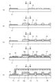
以下、隔壁を有する従来の表示装置について図7を参照して具体的に説明する。図7は、隔壁を有する従来の表示装置の構成の一部を示した模式図であり、図7(a)は、従来の表示装置の平面図、図7(b)は、断面EEにおける従来の表示装置の断面図を示している。 Hereinafter, a conventional display device having a partition wall will be described in detail with reference to FIG. 7A and 7B are schematic views showing a part of the configuration of a conventional display device having a partition wall. FIG. 7A is a plan view of the conventional display device, and FIG. Sectional drawing of the display apparatus of this is shown.
図7に示すように、従来の表示装置1は、基板2と、基板2上にストライプ状に形成された第1電極3と、隣接する第1電極3を画素毎に隔離する隔壁4と、第1電極3上に形成された有機発光層5と、第1電極3の延在方向と直交する方向に有機発光層5上に形成された第2電極6と、第2電極6と接続される迎合電極7とを備えている。
As shown in FIG. 7, a conventional display device 1 includes a
また、従来の表示装置1は、有機発光層5によって画像が表示される表示領域Aと、表示領域Aの外側である表示外領域Bとを有している。第2電極6は、表示領域Aから表示外領域Bに至る領域に亘って形成され、迎合電極7と接続されることにより、迎合電極7を介して外部信号線(図示省略)と接続されるようになっている。
Further, the conventional display device 1 has a display area A in which an image is displayed by the organic
隔壁4は、隣接画素からの光の遮断とインク垂れ防止用壁とを兼ねるために設けられたものであり、フォトリソグラフィ技術によってパターニングされて形成されている。
The
第2電極6は、一般に真空蒸着法によって形成され、例えば図7(b)に示す位置に蒸着源40が設定される。真空蒸着の際に、蒸着源40から放射される電極材料は、ほぼ直線状に進むので、表示外領域Bに設けられた隔壁部4aが障害となり、表示外領域Bにおいて第2電極6を分離する分離領域6aが生じてしまう。特に近年、表示装置の画面サイズの拡大化が図られており、それに伴って基板2の面積が拡大化されている。基板2の面積が拡大されるに従って分離領域6aの発生は顕著になるので、従来の表示装置1は、分離領域6aにおいて抵抗成分の増大や断線が発生しやすくなり、製造歩留が低下して製造コストが増大するという問題があった。
The
この種の問題を解決するための手法としては、例えば特許文献2に示されたものが知られている。特許文献2に示されたものは、パターニングが必要な前述の隔壁とは異なりパターニングが不要の保護層に関するものであり、発光層の上面に設けられる保護層を2層にし、前述の表示領域A及び表示外領域Bにおける保護層の段差を小さくすることによって、保護層上に形成される電極の断線を防止することができるようになっている。
As a technique for solving this type of problem, for example, the technique disclosed in
しかしながら、隔壁を有する表示装置に特許文献2に示された手法を適用しようとすると、隔壁の形成のパターニングに加えてさらに保護層を2層とする工程が必要となるので、製造工数が増大し製造コストが上昇するという問題があった。加えて、隔壁があると、2層に形成された保護層のうち上側の保護層には急峻な面が形成されるので、断線の可能性は依然として解消されず、製造歩留が低下して製造コストが増大するという問題があった。
However, if the technique disclosed in
本発明は、従来の問題を解決するためになされたものであり、従来のものよりも製造コストを低減することができる表示装置を提供するものである。 The present invention has been made to solve the conventional problems, and provides a display device capable of reducing the manufacturing cost as compared with the conventional one.
本発明の表示装置は、基板と、この基板上に設けられた第1電極と、画像が表示される予め定められた表示領域内において前記第1電極上に設けられ画素を形成する発光部と、この発光部上に設けられた第2電極と、前記表示領域とは異なる表示外領域に設けられた第3電極とを備え、前記第2電極は、前記表示外領域に所定の厚さで設けられ前記第3電極と接続する電極接続部を有し、前記電極接続部は、面法線の方向が互いに異なる少なくとも3つの壁面を前記厚さ方向に有し、前記基板から前記第2電極に向かう方向において前記第2電極から所定距離だけ離れた前記表示領域の上方に定められた視点から前記少なくとも3つの壁面を視認した際に、前記少なくとも3つの壁面のうちの少なくとも1つの壁面上に設定された点を起点とする面法線と、前記視点から前記面法線の起点までを結んだ視線とのなす角度が90度以下である構成を有している。 A display device according to the present invention includes a substrate, a first electrode provided on the substrate, and a light emitting unit provided on the first electrode in a predetermined display area in which an image is displayed, and forming a pixel. A second electrode provided on the light emitting portion and a third electrode provided in a display outside region different from the display region, and the second electrode is formed in the display outside region with a predetermined thickness. An electrode connection portion provided to connect to the third electrode, wherein the electrode connection portion includes at least three wall surfaces having different surface normal directions in the thickness direction from the substrate to the second electrode. On at least one of the at least three wall surfaces when the at least three wall surfaces are viewed from a viewpoint defined above the display area that is a predetermined distance away from the second electrode in the direction toward The set point is the starting point That the surface normal, the angle between a sight line that connects to the start point of the surface normal from the viewpoint has a configuration is less than 90 degrees.
この構成により、本発明の表示装置は、第2電極を真空蒸着法によって形成する際の蒸着源が表示領域の上方のいずれに存在しても、第2電極の電極接続部が有する少なくとも3つの壁面のうちの少なくとも1つの壁面が成膜され第2電極と第3電極とを接続することができるので、第2電極と第3電極との間における抵抗成分の増大や断線を防止することができ、従来のものよりも製造コストを低減することができる。 With this configuration, the display device of the present invention has at least three electrode connection portions of the second electrode, regardless of whether the evaporation source for forming the second electrode by the vacuum evaporation method exists above the display region. Since at least one of the wall surfaces is formed and the second electrode and the third electrode can be connected, it is possible to prevent an increase in resistance component or disconnection between the second electrode and the third electrode. The manufacturing cost can be reduced as compared with the conventional one.
また、本発明の表示装置は、前記画素と隣接する画素とを隔離する隔壁を備え、前記隔壁は、前記基板と前記第2電極との間において前記基板上に1μm〜3μm程度の厚さで設けられた構成を有している。 The display device of the present invention includes a partition that separates the pixel from an adjacent pixel, and the partition has a thickness of about 1 μm to 3 μm on the substrate between the substrate and the second electrode. It has a provided configuration.
この構成により、本発明の表示装置は、1μm〜3μm程度の厚さで隣接する画素同士を隔離する隔壁を備えるので、隣接画素からの光を遮断することができ、また、発光部を液体で形成する場合に隣接する画素への液体の流入を防止することができ、さらに、面法線の方向が互いに異なる少なくとも3つの壁面を電極接続部に好適に形成することができる。 With this configuration, the display device of the present invention includes a partition wall that separates adjacent pixels with a thickness of about 1 μm to 3 μm, so that light from the adjacent pixels can be blocked, and the light emitting portion is made of liquid. In the case of forming, it is possible to prevent liquid from flowing into adjacent pixels, and it is possible to suitably form at least three wall surfaces having different surface normal directions from each other in the electrode connection portion.
さらに、本発明の表示装置は、前記第1電極が設けられた前記基板の面と前記少なくとも3つの壁面とがそれぞれなす角度は、40度〜80度程度である構成を有している。 Furthermore, the display device of the present invention has a configuration in which an angle formed between the surface of the substrate on which the first electrode is provided and the at least three wall surfaces is about 40 to 80 degrees.
この構成により、本発明の表示装置は、第2電極を真空蒸着法で形成する場合に安定した膜厚で電極接続部を形成することができるので、第2電極と第3電極との間における抵抗成分の増大や断線を防止することができ、従来のものよりも製造コストを低減することができる。 With this configuration, the display device of the present invention can form the electrode connection portion with a stable film thickness when the second electrode is formed by a vacuum vapor deposition method. Therefore, the display device between the second electrode and the third electrode can be formed. The increase in resistance component and disconnection can be prevented, and the manufacturing cost can be reduced as compared with the conventional one.
さらに、本発明の表示装置は、前記発光部は、印加された電圧によって発光する発光材料を含む溶液が前記第1電極上に塗布されて形成される構成を有している。 Furthermore, the display device of the present invention has a configuration in which the light emitting section is formed by applying a solution containing a light emitting material that emits light by an applied voltage on the first electrode.
この構成により、本発明の表示装置は、真空蒸着法を用いて発光部を形成する従来のものとは異なり、フルカラーの表示機能を持たせる際のシャドーマスクを用いる必要がないので、材料の利用効率を向上させて製造コストの低減化を図ることができ、大画面化や高精細化にも容易に対応することができる。 With this configuration, the display device of the present invention does not need to use a shadow mask for providing a full-color display function, unlike a conventional display device that uses a vacuum evaporation method to form a light emitting portion. The efficiency can be improved and the manufacturing cost can be reduced, and it is possible to easily cope with an increase in screen size and a higher definition.
さらに、本発明の表示装置は、前記発光部は、前記発光材料を含む溶液の液滴が前記第1電極上に吐出されて形成される構成を有している。 Furthermore, in the display device of the present invention, the light emitting section has a configuration in which droplets of a solution containing the light emitting material are formed on the first electrode.
この構成により、本発明の表示装置は、汎用のインクジェット装置を用いて発光部を形成することができるので、材料の利用効率を向上させて製造コストの低減化を図ることができ、大画面化や高精細化にも容易に対応することができる。 With this configuration, the display device of the present invention can form a light-emitting portion using a general-purpose inkjet device, so that the use efficiency of materials can be improved and the manufacturing cost can be reduced, and the screen can be enlarged. And high definition can be easily handled.
さらに、本発明の表示装置は、前記発光部は、リン光発光性を有する材料を含む構成を有している。 Furthermore, in the display device of the present invention, the light emitting section has a configuration including a material having phosphorescence.
この構成により、本発明の表示装置は、蛍光材料を用いる従来のものよりも発光効率を高めることができる。 With this configuration, the display device of the present invention can increase the light emission efficiency as compared with the conventional display using a fluorescent material.
さらに、本発明の表示装置は、前記基板は、可撓性を有すること構成を有している。 Furthermore, the display device of the present invention has a configuration in which the substrate has flexibility.
この構成により、本発明の表示装置は、従来のものよりも製造コストを低減しながら、軽量化、薄型化、フレキシブル化等を図ることができる。 With this configuration, the display device of the present invention can be reduced in weight, thickness, flexibility, etc. while reducing the manufacturing cost as compared with the conventional display device.
さらに、本発明の表示装置は、前記画素毎に少なくとも2つのトランジスタを備えた構成を有している。 Furthermore, the display device of the present invention has a configuration in which at least two transistors are provided for each pixel.
この構成により、本発明の表示装置は、画素の駆動や、発光部の発光制御、トランジスタの特性ばらつきの補正等の機能を複数のトランジスタに持たせることができるので、高い発光効率および輝度を有するフルカラーの高速な動画を表示することができる。 With this structure, the display device of the present invention can have functions such as driving of pixels, light emission control of a light emitting unit, correction of variation in transistor characteristics, and the like in a plurality of transistors, and thus has high light emission efficiency and luminance. Full color high speed video can be displayed.
本発明は、従来のものよりも製造コストを低減することができるという効果を有する表示装置を提供することができるものである。 The present invention can provide a display device having an effect that the manufacturing cost can be reduced as compared with the conventional one.
以下、本発明の実施の形態について図面を用いて説明する。なお、単純マトリクス方式で画素が駆動される表示装置を例に挙げて説明する。 Hereinafter, embodiments of the present invention will be described with reference to the drawings. Note that a display device in which pixels are driven by a simple matrix method will be described as an example.
(第1の実施の形態)
まず、本発明の第1の実施の形態の表示装置の構成について図1を参照して説明する。図1(a)は、本実施の形態に係る表示装置10の断面DDにおける模式的な概略平面図であり、図1(b)は、本実施の形態に係る表示装置10の断面CCにおける模式的な概略断面図である。
(First embodiment)
First, the configuration of the display device according to the first embodiment of the present invention will be described with reference to FIG. Fig.1 (a) is a typical schematic plan view in the cross section DD of the
図1に示すように、本実施の形態に係る表示装置10は、基板11と、基板11上にストライプ状に形成された第1電極12と、隣接する第1電極12を画素毎に隔離する隔壁13と、第1電極12上に形成された有機発光層14と、第1電極12の延在方向と直交する方向に隔壁13及び有機発光層14上に形成された第2電極15と、第2電極15と接続された迎合電極16と、第2電極15上の領域を保護する保護基材17とを備えている。
As shown in FIG. 1, the
また、表示装置10は、有機発光層14によって画像が表示される表示領域Aと、表示領域Aの外側である表示外領域Bとを有している。第2電極15は、表示領域Aから表示外領域Bに至る領域に亘って形成され、迎合電極16と接続されることにより、迎合電極16を介して外部信号線(図示省略)と接続されるようになっている。
In addition, the
なお、以下の記載において、基板11上に第1電極12、有機発光層14及び第2電極15が順次形成される方向を上方向と定義し、上方向の側にある面を上面、その反対側の面を下面という。また、本実施の形態において、第1電極12は、有機発光層14に正孔を注入する陽極とし、また、第2電極15は、有機発光層14に電子を注入する陰極とする。
In the following description, the direction in which the
基板11は、例えばガラスで構成される。また、表示装置10の軽量化、薄型化、フレキシブル化を図る際には、基板11は、例えばポリエーテルスルホンフィルム、ポリカーボネートフィルム等の各種プラスチックフィルムで構成してもよい。各種プラスチックフィルムで基板11を構成することにより、表示装置10は、可撓性を有することとなる。
The
第1電極12は、例えばITO(Indium Tin Oxide:酸化インジウム錫)やIZO(Indium Zinc Oxide:酸化インジウム亜鉛)等の透明電極で構成される。
The
隔壁13は、例えばポリイミド樹脂のような絶縁材料で構成され、表示領域Aにおいて、隣接する画素を隔離するよう基板11上に形成される。一方、表示外領域Bにおいて、隔壁13は、第2電極15と迎合電極16とを接続するために設けられた短冊状隔壁13aを備えている。短冊状隔壁13aは、隔壁13の厚み方向に4つの壁面13b、13c、13d及び13eを備え、壁面13b又は13eと、13cと、13dとは、面法線の方向が互いに異なっている。すなわち、短冊状隔壁13aは、面法線の方向が互いに異なる少なくとも3つの壁面を有する構成となっている。
The
有機発光層14は、例えばポリフェニレンビニレンのような高分子型の有機発光材料で構成されている。なお、例えばジアミン類のような低分子型の有機発光材料で有機発光層14を構成してもよい。有機発光層14は、有機発光材料単体で形成されるもの、又は母体となる有機材料中に発光材料を添加して形成されるものがある。後者の場合は、発光材料の添加率が0.05%〜20%程度であると、発光材料分子間の相互作用により発光効率が極端に低下する濃度消光が起こらず高効率の発光が得られるので好ましい。なお、有機発光層14は、本発明の発光部を構成している。
The organic
また、有機発光層14は、発光効率を高める観点から、リン光発光性を有する材料を用いるのが好ましいが、蛍光材料を用いてもよい。また、有機発光層14は、発光材料と母体材料とを兼ねる、発光成分の基を含む高分子材料(発光性有機化合物、高分子有機化合物)で形成してもよく、このとき、発光成分としてリン光成分を用いるのが、より好ましい。
The organic
第2電極15は、例えばアルミニウム、金、マグネシウム−銀合金等で構成され、表示領域Aにおいて、隔壁13及び有機発光層14の上面に形成される。一方、表示外領域Bにおいて、第2電極15は、表示領域A側の第2電極15と迎合電極16とを電気的に接続する第1接続部15aと第2接続部15fとを備えている。
The
第1接続部15aは、短冊状隔壁13aが有する4つの壁面13b、13c、13d及び13eの上面にそれぞれ形成された第2電極15の4つの壁面15b、15c、15d及び15eを備えている。すなわち、壁面15b又は15eと、15cと、15dとは、面法線の方向が互いに異なっているので、第1接続部15aは、面法線の方向が互いに異なる少なくとも3つの壁面を有する構成となっている。なお、第1接続部15aは、本発明の電極接続部を構成している。
The
第2接続部15fは、第1接続部15aの4つの壁面15b、15c、15d及び15eのうちの少なくとも1つと、迎合電極16とを電気的に接続するようになっている。なお、第2接続部15fは、本発明の電極接続部を構成している。
The
迎合電極16は、例えばアルミニウム、金、マグネシウム−銀合金等で構成される。迎合電極16は、第1接続部15aの4つの壁面15b、15c、15d及び15eのうちの少なくとも1つの壁面を介し、表示領域A側の第2電極15と電気的に接続されるようになっている。なお、迎合電極16は、本発明の第3電極を構成している。
The
保護基材17は、例えばガラスで構成され、表示領域Aの全体を覆って外部からの酸素雰囲気や水蒸気等による有機発光層14の劣化を防止するようになっている。
The
本実施の形態に係る表示装置10は、前述のように構成されており、第1電極12と第2電極15との間に所定の電圧の信号が入力されると、信号が入力された画素位置の有機発光層14に電子と正孔とが注入され、これらが再結合することによって該当する有機発光層14から光が放射され、所定の画像が基板11上に表示される。
The
次に、本実施の形態の表示装置10の製造方法について図1〜図3を参照して説明する。図2(a)〜(e)は、各製造工程における表示装置10の概略断面図である。また、図3は、表示外領域Bにおける第2電極15の概略斜視図である。なお、以下の製造工程の説明において記載した製造上の手法や寸法等は一例であり、本発明はこれらに限定されるものではない。
Next, a method for manufacturing the
まず、表示外領域Bの基板11上に迎合電極16として例えばアルミニウムを100nm〜500nm程度の厚さで形成した後、表示領域Aの基板11上に第1電極12として例えばITOを100nm〜500nm程度の厚さでストライプ状に形成する(図2(a))。迎合電極16及び第1電極12の形成工程は、例えばスパッタリング法、真空蒸着法等を用いることができる。なお、第1電極12を形成した後に迎合電極16を形成する順序としてもよい。
First, after forming aluminum as the
次いで、例えばフォトリソグラフィ技術によって、第1電極12の画素形成に使用する領域以外の領域に、例えばポリイミド樹脂の絶縁膜を成膜し、隣接する画素同士を隔離する隔壁13をパターニングして形成する(図2(b))。このとき、表示外領域Bにおいては、図1(a)に示すように、4つの壁面13b、13c、13d及び13eを含む短冊状隔壁13aをパターニングして形成する。実験結果によれば、隔壁13の膜厚としては、1μm〜3μm程度が好ましく、4つの壁面13b、13c、13d及び13eがそれぞれ基板11の面となす角度は、40度〜80度程度が好ましい。
Next, an insulating film made of, for example, polyimide resin is formed in a region other than the region used for pixel formation of the
続いて、第1電極12上に有機発光層14として例えば高分子型有機材料を10nm〜200nm程度の厚さで形成する(図2(c))。高分子型有機材料で有機発光層14を形成する手法としては、例えばインクジェット装置を用いて高分子型有機材料の溶液を射出するインクジェットプリント法がある。なお、低分子型有機材料を用いて、例えば真空蒸着法により有機発光層14を形成してもよい。
Subsequently, for example, a polymer organic material is formed on the
ここで、有機発光層14は、単一の層であってもよく、また、有機薄膜を有機発光層14の上下に積層した有機薄膜積層構造であってもよい。有機薄膜積層構造の具体例を挙げれば、例えば、陽極としての第1電極12から注入される正孔を中継して輸送する正孔輸送層を有機発光層14の下面に、また、後述する工程で形成される陰極としての第2電極15から注入される電子を中継して輸送する電子輸送層を有機発光層14の上面に設ける構成がある。
Here, the organic
なお、第1電極12と有機発光層14との間に導電性高分子層を形成しておくと、有機発光層14への正孔注入を容易に行わせることができて好適である。導電性高分子層としては、例えばポリアニリン、ポリチオフェン誘導体であるPEDT:PSS(poly(ethylenedioxythiophene):poly(styrenesulfonate))等を挙げることができる。
It is preferable that a conductive polymer layer be formed between the
引き続き、例えば真空蒸着法により、隔壁13及び有機発光層14の上面に、第1電極12と直交するようにストライプ状の第2電極15を100nm〜500nm程度の膜厚で形成する(図2(d))。このとき、表示外領域Bにおいて、第1接続部15a(図1参照)は、面法線の方向が互いに異なる少なくとも3つの壁面を有する短冊状隔壁13a上に形成されるので、図3に示すように、面法線の方向が互いに異なる3つの壁面15b、15c及び15dと、面法線の方向が壁面15bと同じである壁面15eとが形成される。
Subsequently, a striped
すなわち、従来のものは、壁面15eに相当する壁面のみであったが、本実施の形態に係る第2電極15は、第1電極12が形成された基板11の面と平行な面法線成分が壁面15eのものと90度異なる壁面15c及び15dを有している。
That is, although the conventional one is only the wall surface corresponding to the
ここで、図3に示すように、第2電極15を形成するための蒸着源40が表示領域A上に存在する場合、壁面15d上に設定された点P1を起点とする面法線と、蒸着源40を視点として点P1を視認したときの視線とのなす角度をθ1とし、同様に、壁面15c上に設定された点P2を起点とする面法線と、蒸着源40を視点として点P2を視認したときの視線とのなす角度をθ2としたとき、蒸着源40が表示領域Aの上方にあれば、θ1及びθ2のいずれか一方は必ず90度以下になる。
Here, as shown in FIG. 3, when the
したがって、壁面15b及び15eと第2接続部15fとの間において蒸着膜が安定して成膜されない場合でも、壁面15c及び15dのいずれか一方と第2接続部15fとの間は必ず成膜されて電気的に接続されるので、本実施の形態に係る第2電極15は、表示領域A側の第2電極15と迎合電極16との間において、断線や抵抗増加等を発生させることなく安定した電気的接続を行うことができる。
Therefore, even when a vapor deposition film is not stably formed between the wall surfaces 15b and 15e and the
なお、有機発光層14と第2電極15との間に仕事関数の小さい金属及びその金属化合物を例えば0.1nm〜20nm程度の膜厚で形成すれば、第2電極15から有機発光層14への電子の注入が容易になるので好適である。仕事関数の小さい金属としては、例えば、アルカリ金属のLi、Na、K、Rb、Cs等や、アルカリ土類金属のBe、Mg、Ca、Sr、Ba等があり、これらの金属の化合物としては、MgAg、MgO、LiF、LiO2、NaF、CsF等がある。
If a metal having a small work function and its metal compound are formed between the organic
次いで、第2電極15上を覆うように保護基材17を形成し(図2(e))、第2電極15と保護基材17との間の空洞部には例えば窒素及び乾燥剤を充填する。保護基材17の形成には、例えば接着剤を用いて第2電極15と接着する方法や、酸素雰囲気や水蒸気の侵入をブロックするシリコン窒化層(SiNx)、シリコン酸化層(SiOx)又はシリコン窒化酸化層(SiON)等を第2電極15上に直接形成する方法等がある。
Next, the
以上のように、本実施の形態の表示装置10によれば、第2電極15を真空蒸着法によって形成する際の蒸着源40が表示領域Aの上方のいずれに存在しても、第2電極15の第1接続部15aが有する少なくとも3つの壁面のうちの少なくとも1つの壁面が成膜され第2電極15と迎合電極16とを接続する構成としたので、第2電極15と迎合電極16との間における抵抗成分の増大や断線を防止することができ、従来のものよりも製造コストを低減することができる。
As described above, according to the
また、本実施の形態の表示装置10によれば、基板11上に隔壁13を形成して隣接する画素同士を隔離する構成としたので、隣接画素からの光を遮断することができ、また、液体で有機発光層14を形成する際に隣接する画素への液体の流入を防止することができる。また、隔壁13の厚さを1μm〜3μm程度としたので、面法線の方向が互いに異なる少なくとも3つの壁面を電極接続部に好適に形成することができる。
Further, according to the
さらに、本実施の形態の表示装置10によれば、短冊状隔壁13aが有する4つの壁面13b、13c、13d及び13eがそれぞれ基板11の面となす角度を40度〜80度程度とする構成としたので、第2電極15を真空蒸着法等で形成する場合に安定した膜厚で、4つの壁面15b、15c、15d及び15eを成膜することができ、第2電極15と迎合電極16との間における抵抗成分の増大や断線を防止して、従来のものよりも製造コストを低減することができる。
Furthermore, according to the
さらに、本実施の形態の表示装置10によれば、ポリフェニレンビニレンのような高分子型の有機発光材料でインクジェットプリント法を用いて有機発光層14を形成する構成としたので、真空蒸着法を用いて発光部を形成する従来のものとは異なり、フルカラーの表示機能を持たせる際のシャドーマスクを用いる必要がないので、材料の利用効率を向上させて製造コストの低減化を図ることができ、大画面化や高精細化にも容易に対応することができる。
Further, according to the
さらに、本実施の形態の表示装置10によれば、ポリフェニレンビニレンのような高分子型の有機発光材料でインクジェットプリント法を用いて有機発光層14を形成する構成としたので、汎用のインクジェット装置を用いて有機発光層14を形成することができるので、材料の利用効率を向上させて製造コストの低減化を図ることができ、大画面化や高精細化にも容易に対応することができる。
Further, according to the
なお、本実施の形態において、有機発光層14で発光部を構成する例を挙げて説明したが、本発明はこれに限定されるものではなく、印加された電圧によって発光する発光材料を含むもので発光部を構成すれば同様の効果が得られる。
In this embodiment, the example in which the organic
また、本実施の形態において、表示装置10は単純マトリクス方式で駆動されるものとして説明したが、本発明はこれに限定されるものではなく、アクティブマトリクス方式で駆動するものであっても同様の効果が得られる。アクティブマトリクス方式で駆動する場合、TFT(Thin Film Transistor)素子が基板11と隔壁13との間に形成され、第1電極12が画素毎にパターニングされて形成され、且つそれぞれの第1電極12にTFT素子が接続される構成とすることができる。このとき、画素毎に駆動源として少なくとも2個のTFTを設けると、高い発光効率および輝度を有するフルカラーの高速な動画表示を得ることができるので好ましい。
Further, in the present embodiment, the
具体的には、例えば図4に示すように、駆動させる画素をスイッチング動作により制御するTFT41と、有機発光層14を表したダイオード43の駆動をスイッチング動作により制御するTFT42とを備える構成とすることができる。また、TFTをさらに増設してパネル内のTFT特性のばらつきを補正する作用を持たせることにより、より安定した表示を行わせることが可能となる。
Specifically, for example, as shown in FIG. 4, the
(第2の実施の形態)
本発明の第2の実施の形態の表示装置の構成について図5を参照して説明する。図5は、本実施の形態に係る表示装置20の模式的な概略平面図である。
(Second Embodiment)
The configuration of the display device according to the second embodiment of the present invention will be described with reference to FIG. FIG. 5 is a schematic schematic plan view of the
図5に示すように、本実施の形態に係る表示装置20は、本発明の第1の実施の形態に係る表示装置10(図1参照)と比較して、形状が異なる第2電極25を備えたものである。したがって、第2電極25に係る構成以外の説明及び重複する説明は省略する。なお、図5において、基板21及び迎合電極26は、それぞれ、表示装置10の基板11及び迎合電極16と対応するものである。
As shown in FIG. 5, the
第2電極25は、例えばアルミニウム、金、マグネシウム−銀合金等で構成され、表示領域Aにおいて、本発明の第1の実施の形態に係る表示装置10と同様に、隔壁23及び有機発光層(図示省略)の上面に形成される。一方、表示外領域Bにおいて、第2電極25は、表示領域A側の第2電極25と迎合電極26とを電気的に接続する第1接続部25aと第2接続部25fとを備えている。
The
第1接続部25aは、4つの壁面25b、25c、25d及び25eを備えている。壁面25b又は25eと、25cと、25dとは、面法線の方向が互いに異なっているので、第1接続部25aは、面法線の方向が互いに異なる少なくとも3つの壁面を有する構成となっている。
The first connecting
第2接続部25fは、4つの壁面25b、25c、25d及び25eのうちの少なくとも1つと、迎合電極26とを電気的に接続するようになっている。
The second connecting
なお、図5において、第1接続部25aの下面側に形成された短冊状隔壁23aの詳細な図示を省略したが、本実施の形態に係る表示装置20は、図1に示された本発明の第1の実施の形態に係る表示装置10と同様に、第1接続部25aの4つの壁面25b、25c、25d及び25eをそれぞれ形成するための壁面を有する短冊状隔壁23aを備えている。
In FIG. 5, the detailed illustration of the strip-shaped
以上のように、本実施の形態の表示装置20によれば、第2電極25を真空蒸着法によって形成する際の蒸着源が表示領域Aの上方のいずれに存在しても、第2電極25の第1接続部25aが有する少なくとも3つの壁面のうちの少なくとも1つの壁面が成膜され第2電極25と迎合電極26とを接続する構成としたので、第2電極25と迎合電極26との間における抵抗成分の増大や断線を防止することができ、従来のものよりも製造コストを低減することができる。
As described above, according to the
(第3の実施の形態)
本発明の第3の実施の形態の表示装置の構成について図6を参照して説明する。図6は、本実施の形態に係る表示装置30の模式的な概略平面図である。
(Third embodiment)
The configuration of the display device according to the third embodiment of the present invention will be described with reference to FIG. FIG. 6 is a schematic schematic plan view of the
図6に示すように、本実施の形態係る表示装置30は、本発明の第1の実施の形態に係る表示装置10(図1参照)と比較して、形状が異なる第2電極35を備えたものである。したがって、第2電極35に係る構成以外の説明及び重複する説明は省略する。なお、図6において、基板31及び迎合電極36は、それぞれ、表示装置10の基板11及び迎合電極16と対応するものである。
As shown in FIG. 6, the
第2電極35は、例えばアルミニウム、金、マグネシウム−銀合金等で構成され、表示領域Aにおいて、本発明の第1の実施の形態に係る表示装置10と同様に、隔壁33及び有機発光層(図示省略)の上面に形成される。一方、表示外領域Bにおいて、第2電極35は、表示領域A側の第2電極35と迎合電極36とを電気的に接続する第1接続部35aと第2接続部35gとを備えている。
The
第1接続部35aは、5つの壁面35b、35c、35d、35e及び35fを備えている。壁面35b又は35fと、35cと、35dと、35eとは、面法線の方向が互いに異なっているので、第1接続部35aは、面法線の方向が互いに異なる少なくとも4つの壁面を有する構成となっている。
The
第2接続部35gは、5つの壁面35b、35c、35d、35e及び35fのうちの少なくとも1つと、迎合電極36とを電気的に接続するようになっている。
The
なお、図6において、第1接続部35aの下面側に形成された短冊状隔壁33aの詳細な図示を省略したが、本実施の形態に係る表示装置30は、図1に示された本発明の第1の実施の形態に係る表示装置10と同様に、第1接続部35aの5つの壁面35b、35c、35d、35e及び35fをそれぞれ形成するための壁面を有する短冊状隔壁33aを備えている。
In FIG. 6, the detailed illustration of the strip-shaped
以上のように、本実施の形態の表示装置30によれば、第2電極35を真空蒸着法によって形成する際の蒸着源が表示領域Aの上方のいずれに存在しても、第2電極35の第1接続部35aが有する少なくとも3つの壁面のうちの少なくとも1つの壁面が成膜され第2電極35と迎合電極36とを接続する構成としたので、第2電極35と迎合電極36との間における抵抗成分の増大や断線を防止することができ、従来のものよりも製造コストを低減することができる。
As described above, according to the
10、20、30 表示装置
11、21、31 基板
12 第1電極
13、23、33 隔壁
13a、23a、33a 短冊状隔壁
13b〜13e 短冊状隔壁の壁面
14 有機発光層(発光部)
15、25、35 第2電極
15a、25a、35a 第1接続部(電極接続部)
15b〜15e、25b〜25e、35b〜35f 第2電極の壁面
15f、25f、35g 第2接続部(電極接続部)
16、26、36 迎合電極(第3電極)
17 保護基材
40 蒸着源
41、42 TFT(トランジスタ)
43 ダイオード
10, 20, 30
15, 25, 35
15b-15e, 25b-25e, 35b-35f Wall surface of
16, 26, 36 Compliant electrode (third electrode)
17
43 Diode
Claims (8)
前記第2電極は、前記表示外領域に所定の厚さで設けられ前記第3電極と接続する電極接続部を有し、
前記電極接続部は、面法線の方向が互いに異なる少なくとも3つの壁面を前記厚さ方向に有し、
前記基板から前記第2電極に向かう方向において前記第2電極から所定距離だけ離れた前記表示領域の上方に定められた視点から前記少なくとも3つの壁面を視認した際に、前記少なくとも3つの壁面のうちの少なくとも1つの壁面上に設定された点を起点とする面法線と、前記視点から前記面法線の起点までを結んだ視線とのなす角度が90度以下であることを特徴とする表示装置。 A substrate, a first electrode provided on the substrate, a light emitting unit provided on the first electrode in a predetermined display area where an image is displayed, and forming a pixel, and provided on the light emitting unit A second electrode provided, and a third electrode provided in a non-display area different from the display area,
The second electrode has an electrode connection portion provided at a predetermined thickness in the outside display area and connected to the third electrode,
The electrode connecting portion has at least three wall surfaces in the thickness direction, the directions of the surface normals being different from each other,
When the at least three wall surfaces are viewed from a viewpoint defined above the display area that is separated from the second electrode by a predetermined distance in a direction from the substrate toward the second electrode, of the at least three wall surfaces. An angle formed by a surface normal starting from a point set on at least one wall surface of the screen and a line of sight connecting from the viewpoint to the starting point of the surface normal is 90 degrees or less. apparatus.
Priority Applications (1)
| Application Number | Priority Date | Filing Date | Title |
|---|---|---|---|
| JP2005188427A JP4880923B2 (en) | 2005-06-28 | 2005-06-28 | Display device |
Applications Claiming Priority (1)
| Application Number | Priority Date | Filing Date | Title |
|---|---|---|---|
| JP2005188427A JP4880923B2 (en) | 2005-06-28 | 2005-06-28 | Display device |
Publications (2)
| Publication Number | Publication Date |
|---|---|
| JP2007010761A true JP2007010761A (en) | 2007-01-18 |
| JP4880923B2 JP4880923B2 (en) | 2012-02-22 |
Family
ID=37749411
Family Applications (1)
| Application Number | Title | Priority Date | Filing Date |
|---|---|---|---|
| JP2005188427A Expired - Fee Related JP4880923B2 (en) | 2005-06-28 | 2005-06-28 | Display device |
Country Status (1)
| Country | Link |
|---|---|
| JP (1) | JP4880923B2 (en) |
Cited By (3)
| Publication number | Priority date | Publication date | Assignee | Title |
|---|---|---|---|---|
| WO2008126263A1 (en) * | 2007-03-30 | 2008-10-23 | Pioneer Corporation | Organic electroluminescence device and process for manufacturing the same |
| JP2010108623A (en) * | 2008-10-28 | 2010-05-13 | Toppan Forms Co Ltd | Electronic panel |
| JP2013229258A (en) * | 2012-04-26 | 2013-11-07 | Konica Minolta Inc | Organic semiconductor element and method for manufacturing the same |
Citations (4)
| Publication number | Priority date | Publication date | Assignee | Title |
|---|---|---|---|---|
| JPS6192978U (en) * | 1984-11-24 | 1986-06-16 | ||
| JPH1124094A (en) * | 1997-06-30 | 1999-01-29 | Matsushita Electric Ind Co Ltd | Liquid crystal display device |
| JP2002231445A (en) * | 2001-01-31 | 2002-08-16 | Dainippon Printing Co Ltd | El element and method of manufacture |
| JP2002287663A (en) * | 2001-03-28 | 2002-10-04 | Hitachi Ltd | Display device |
-
2005
- 2005-06-28 JP JP2005188427A patent/JP4880923B2/en not_active Expired - Fee Related
Patent Citations (4)
| Publication number | Priority date | Publication date | Assignee | Title |
|---|---|---|---|---|
| JPS6192978U (en) * | 1984-11-24 | 1986-06-16 | ||
| JPH1124094A (en) * | 1997-06-30 | 1999-01-29 | Matsushita Electric Ind Co Ltd | Liquid crystal display device |
| JP2002231445A (en) * | 2001-01-31 | 2002-08-16 | Dainippon Printing Co Ltd | El element and method of manufacture |
| JP2002287663A (en) * | 2001-03-28 | 2002-10-04 | Hitachi Ltd | Display device |
Cited By (5)
| Publication number | Priority date | Publication date | Assignee | Title |
|---|---|---|---|---|
| WO2008126263A1 (en) * | 2007-03-30 | 2008-10-23 | Pioneer Corporation | Organic electroluminescence device and process for manufacturing the same |
| JPWO2008126263A1 (en) * | 2007-03-30 | 2010-07-22 | パイオニア株式会社 | Organic electroluminescence device and manufacturing method thereof |
| JP5015237B2 (en) * | 2007-03-30 | 2012-08-29 | パイオニア株式会社 | Manufacturing method of organic EL display panel |
| JP2010108623A (en) * | 2008-10-28 | 2010-05-13 | Toppan Forms Co Ltd | Electronic panel |
| JP2013229258A (en) * | 2012-04-26 | 2013-11-07 | Konica Minolta Inc | Organic semiconductor element and method for manufacturing the same |
Also Published As
| Publication number | Publication date |
|---|---|
| JP4880923B2 (en) | 2012-02-22 |
Similar Documents
| Publication | Publication Date | Title |
|---|---|---|
| US11963415B2 (en) | Display device including a power supply line that overlaps a driving circuit | |
| JP6218548B2 (en) | Organic light emitting display | |
| KR102166341B1 (en) | Organic Light Emitting Diode Display Having High Aperture Ratio And Method For Manufacturing The Same | |
| KR102081317B1 (en) | High Aperture Ratio Organic Light Emitting Diode Display Having Double Bank Structure | |
| WO2014136149A1 (en) | El display device | |
| US20130257839A1 (en) | Organic Light Emitting Diode Display | |
| US20070200488A1 (en) | Display device | |
| US20140091287A1 (en) | Organic el device, method for manufacturing the same, and electronic apparatus | |
| JP2005258395A (en) | Electroluminescence display device | |
| KR100739065B1 (en) | Organic light emitting display and method for fabricating thereof | |
| US20230209909A1 (en) | Display device and method of manufacturing the same | |
| US7294960B2 (en) | Organic electroluminescent device with HIL/HTL specific to each RGB pixel | |
| JP4880923B2 (en) | Display device | |
| JP2006260950A (en) | Organic el device, manufacturing method of the same, and electronic device | |
| JP2008541393A5 (en) | ||
| KR101577832B1 (en) | Organic Light Emitting Display Device and Shadowmask | |
| US9210764B2 (en) | Organic light emitting diode device and method of manufacturing the same | |
| KR100739651B1 (en) | Organic light emitting diode display device and fabrication method thereof | |
| KR100387722B1 (en) | Organic Electro Luminescence Display with a Double Pixel structure | |
| KR101115974B1 (en) | Transistor, display device, electronic device, and fabrication method for transistor | |
| JP2007188779A (en) | Organic el display device | |
| EP4207974A1 (en) | Organic light emitting display device and method for manufacturing the same | |
| KR101839331B1 (en) | Method for fabricating the organic light emitting display device | |
| KR101613730B1 (en) | Organic Light Emitting Display Device and Manufacturing Method thereof | |
| KR100740134B1 (en) | Organic light emitting diode display device and fabrication method thereof |
Legal Events
| Date | Code | Title | Description |
|---|---|---|---|
| A621 | Written request for application examination |
Free format text: JAPANESE INTERMEDIATE CODE: A621 Effective date: 20080122 |
|
| A977 | Report on retrieval |
Free format text: JAPANESE INTERMEDIATE CODE: A971007 Effective date: 20110302 |
|
| A131 | Notification of reasons for refusal |
Free format text: JAPANESE INTERMEDIATE CODE: A131 Effective date: 20110405 |
|
| A521 | Request for written amendment filed |
Free format text: JAPANESE INTERMEDIATE CODE: A523 Effective date: 20110511 |
|
| A131 | Notification of reasons for refusal |
Free format text: JAPANESE INTERMEDIATE CODE: A131 Effective date: 20110802 |
|
| A521 | Request for written amendment filed |
Free format text: JAPANESE INTERMEDIATE CODE: A523 Effective date: 20110915 |
|
| TRDD | Decision of grant or rejection written | ||
| A01 | Written decision to grant a patent or to grant a registration (utility model) |
Free format text: JAPANESE INTERMEDIATE CODE: A01 Effective date: 20111108 |
|
| A01 | Written decision to grant a patent or to grant a registration (utility model) |
Free format text: JAPANESE INTERMEDIATE CODE: A01 |
|
| A61 | First payment of annual fees (during grant procedure) |
Free format text: JAPANESE INTERMEDIATE CODE: A61 Effective date: 20111202 |
|
| R150 | Certificate of patent or registration of utility model |
Free format text: JAPANESE INTERMEDIATE CODE: R150 |
|
| FPAY | Renewal fee payment (event date is renewal date of database) |
Free format text: PAYMENT UNTIL: 20141209 Year of fee payment: 3 |
|
| R250 | Receipt of annual fees |
Free format text: JAPANESE INTERMEDIATE CODE: R250 |
|
| R250 | Receipt of annual fees |
Free format text: JAPANESE INTERMEDIATE CODE: R250 |
|
| LAPS | Cancellation because of no payment of annual fees |