JP2007227452A - Flexible wiring board, its solder bonding method and optical transmitting package using the same - Google Patents
Flexible wiring board, its solder bonding method and optical transmitting package using the same Download PDFInfo
- Publication number
- JP2007227452A JP2007227452A JP2006044041A JP2006044041A JP2007227452A JP 2007227452 A JP2007227452 A JP 2007227452A JP 2006044041 A JP2006044041 A JP 2006044041A JP 2006044041 A JP2006044041 A JP 2006044041A JP 2007227452 A JP2007227452 A JP 2007227452A
- Authority
- JP
- Japan
- Prior art keywords
- solder
- electrode
- wiring board
- flexible wiring
- film
- Prior art date
- Legal status (The legal status is an assumption and is not a legal conclusion. Google has not performed a legal analysis and makes no representation as to the accuracy of the status listed.)
- Pending
Links
Images


Abstract
Description
この発明は、電子部品の電極間を接続するフレキシブル配線基板と、そのフレキシブル配線基板を電極にはんだ接合するフレキシブル配線基板のはんだ接合方法と、フレキシブル配線基板を用いて発光素子と電極とを接続した光送信パッケージに関するものである。 The present invention relates to a flexible wiring board for connecting electrodes of an electronic component, a soldering method for a flexible wiring board for soldering the flexible wiring board to an electrode, and a light emitting element and an electrode connected using the flexible wiring board. The present invention relates to an optical transmission package.
複数の電子部品間を立体的に配置し、それらを電気的に接続する方法として、可とう性に優れたフレキシブル配線基板を用いて接続する方法がよく用いられる。
フレキシブル配線基板を用いて、電子部品間を接続する方法として、エポキシ樹脂接着剤中に導電性粒子を含有した異方性導電接着フィルムを用いる方法と、はんだを用いる方法とが通常用いられる。
異方性導電接着フィルムを用いる方法は、エポキシ樹脂の接着力で電極と導電粒子が接触することによって電気的接続を得るため、接続の信頼性が低い。それに対し、はんだを用いる方法は、はんだにて電極間を金属接合するので、接続信頼性が高く、接続抵抗も小さい。
はんだで接合する場合、あらかじめ電子部品の電極上またはフレキシブル配線基板の電極上にはんだを形成しておき、電極同士の位置合わせを行った後、フレキシブル配線基板の電極を加熱ツールによって押し当てることによって、はんだを溶融させて、はんだ接合を実現する。はんだを溶融させた時に、はんだが配線に沿って流れ出ないように、配線部分がソルダーレジストと呼ばれる樹脂または接着剤で貼ったポリイミドフィルムで覆われている。
したがって、従来のフレキシブル配線基板の構造は、ポリイミドフィルム上に導体が形成され、導体は信号を伝送するための配線と接合用の電極になり、接合に供する電極を除く配線領域上にはソルダーレジストまたはポリイミドフィルムが接着剤で貼り付けられている。(特許文献1参照)
As a method of arranging a plurality of electronic components in a three-dimensional manner and electrically connecting them, a method of connecting using a flexible wiring board having excellent flexibility is often used.
As a method for connecting electronic components using a flexible wiring board, a method using an anisotropic conductive adhesive film containing conductive particles in an epoxy resin adhesive and a method using solder are usually used.
In the method using the anisotropic conductive adhesive film, since the electrode and the conductive particles are brought into contact with each other by the adhesive force of the epoxy resin, the connection reliability is low. On the other hand, in the method using solder, since the electrodes are metal-bonded with solder, the connection reliability is high and the connection resistance is small.
When joining with solder, by forming solder on the electrodes of the electronic component or the electrodes of the flexible wiring board in advance, aligning the electrodes, and then pressing the electrodes of the flexible wiring board with a heating tool , Solder is melted to realize solder joint. The wiring portion is covered with a polyimide film pasted with a resin called a solder resist or an adhesive so that the solder does not flow along the wiring when the solder is melted.
Therefore, the structure of a conventional flexible wiring board is that a conductor is formed on a polyimide film, and the conductor becomes a wiring for transmitting a signal and an electrode for bonding, and a solder resist is formed on the wiring region excluding the electrode for bonding. Or the polyimide film is affixed with the adhesive agent. (See Patent Document 1)
ところで、パッケージ内の電極間の接続にフレキシブル配線基板を用いる場合、電極からフレキシブル配線基板の配線へのはんだの流れ防止に用いるソルダーレジスト及びポリイミドフィルムを貼り付けた接着剤から、高温時に腐食性のガスが発生することがある。
具体的には、樹脂の硬化に用いたアミン基が水分と結合してアンモニアガスになる。または樹脂中のハロゲンがガス化して腐食要因になる。
ガスが発生すると、他の半導体素子または電子部品または接合部が腐食され、パッケージの信頼性が低下する問題がある。
By the way, when a flexible wiring board is used for the connection between the electrodes in the package, it is corrosive at a high temperature from the adhesive to which the solder resist and the polyimide film used for preventing the flow of solder from the electrodes to the wiring of the flexible wiring board are attached. Gas may be generated.
Specifically, the amine group used for curing the resin is combined with moisture to become ammonia gas. Or the halogen in the resin is gasified to cause corrosion.
When the gas is generated, other semiconductor elements or electronic components or joints are corroded, and there is a problem that the reliability of the package is lowered.
この発明は、上述のような課題を解決するためになされたものであり、腐食性のガスを発生することなく、電極間をはんだ接合できるフレキシブル配線基板及びそのはんだ接合方法並びにこれを用いた光送受信パッケージを得ることを目的にしている。 The present invention has been made to solve the above-described problems, and is a flexible wiring board capable of solder-bonding electrodes without generating corrosive gas, a solder-joining method thereof, and a light using the same. The purpose is to obtain a sending and receiving package.
この発明に係わるフレキシブル配線基板においては、耐熱絶縁フィルム上に形成された導体は、接合に用いられる電極と電極間を接続する配線からなり、配線上には、はんだに濡れない膜が形成されると共に、電極上には、はんだに濡れる膜が形成されているものである。 In the flexible wiring board according to the present invention, the conductor formed on the heat-resistant insulating film is composed of an electrode used for bonding and a wiring connecting the electrodes, and a film that does not wet with solder is formed on the wiring. At the same time, a film that gets wet with solder is formed on the electrode.
この発明は、以上説明したように、耐熱絶縁フィルム上に形成された導体は、接合に用いられる電極と電極間を接続する配線からなり、配線上には、はんだに濡れない膜が形成されると共に、電極上には、はんだに濡れる膜が形成されているので、はんだ接合時に溶融したはんだが配線に流れ出すことがなく、電気的特性が向上すると共に、はんだが配線に流れ出すのを防ぐためのソルダーレジストや耐熱温度の低い接着剤を用いる必要がなく、このため腐食性のガスの発生もない。 In the present invention, as described above, the conductor formed on the heat-resistant insulating film is composed of an electrode used for bonding and a wiring connecting the electrodes, and a film that does not wet with solder is formed on the wiring. At the same time, a film that wets the solder is formed on the electrode, so that the molten solder does not flow out to the wiring at the time of soldering, the electrical characteristics are improved, and the solder is prevented from flowing out to the wiring. It is not necessary to use a solder resist or an adhesive having a low heat resistance temperature, and therefore no corrosive gas is generated.
実施の形態1.
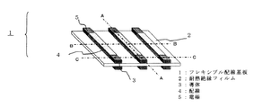
図1は、この発明の実施の形態1によるフレキシブル配線基板を示す斜視図である。
図1において、フレキシブル配線基板1は、耐熱絶縁フィルム2上に直に形成された導体3と、この導体3上をはんだに濡れにくい膜で覆うことによって構成される配線4と、さらに配線4の表面をはんだに濡れやすい膜で覆うことによって形成した電極5(基板側電極)とにより構成される。
1 is a perspective view showing a flexible wiring board according to
In FIG. 1, a
図2は、この発明の実施の形態1によるフレキシブル配線基板を示す断面図であり、図2(a)は、図1のA−A断面図、図2(b)は、図1のB−B断面図、図2(c)は、図1のC−C断面図である。
図2において、1、2、3は図1におけるものと同一のものである。導体3上をはんだに濡れにくい膜41で覆い、配線4の表面をはんだに濡れやすい膜51で覆い、電極としている。
2 is a cross-sectional view showing a flexible wiring board according to
In FIG. 2, 1, 2, and 3 are the same as those in FIG. The
次に、動作について説明する。
導体3は、耐熱絶縁フィルム2上に直に形成される。この形成方法は、耐熱絶縁フィルム2上にスパッタ、蒸着またはめっきなどの方法で形成し、写真製版でパターニングする方法と、金属膜上に耐熱絶縁膜を形成した後で、写真製版によって金属膜をパターニングする方法とがある。
ここで、耐熱絶縁フィルム2の材料としては、可とう性があって、200°C以上の耐熱性を有する樹脂フィルムが用いられ、例えば、ポリイミド、液晶ポリマーなどがある。導体3としては、熱伝導がよく、電気抵抗が小さい材料がよく、例えば銅がよい。
Next, the operation will be described.
The
Here, as a material of the heat-resistant
配線4は、導体3上をはんだに濡れにくい膜41で覆うことによって構成される。このはんだに濡れにくい膜41の材料としては、クロム、アルミニューム、モリブデンなどの金属でもよいが、金属の酸化膜が簡便で安価である。ここでは、ニッケルの酸化膜を用いた。ニッケルの酸化膜は、はんだに濡れにくいだけでなく耐食性もある。具体的には、導体3上にニッケルをめっきで、数μm形成し、空気中で酸化させる方法を用いた。
The
電極5の表面は、はんだに濡れやすい膜51で覆われる。はんだに濡れやすい膜51の材料としては金がある。具体的には、導体3上にニッケルめっきを全面に施した後、配線部分をレジストで覆い、電極部分を露出した後、金めっきを施し、レジストを剥離することによって形成した。したがって、電極5のはんだに濡れやすい膜51は、ニッケル上に金めっきで形成される。
なお、はんだへの濡れ性は、電極の表面と、溶融させたはんだの液滴とのなす角度(接触角)で表される。濡れがよいものは、はんだがよく広がり、接触角が鋭角となる。逆に、はんだに濡れにくいと、はんだが広がらず、球になろうとするため、接触角は鈍角となる。
The surface of the
The wettability to solder is expressed by an angle (contact angle) between the surface of the electrode and a molten solder droplet. In the case of good wettability, the solder spreads well and the contact angle becomes an acute angle. Conversely, if the solder is difficult to wet, the solder does not spread and tends to become a sphere, so the contact angle becomes an obtuse angle.
また、図1と図2では、耐熱絶縁フィルム2の両面に導体3を形成した場合を示したが、導体3は耐熱絶縁フィルム2の片面に形成したものであってもよい。
また、耐熱絶縁フィルム2の表裏の電極5および配線4に、耐熱絶縁フィルム2を貫通して互いに接続するスルーホールを設けてもよい。
1 and 2 show the case where the
Moreover, you may provide the through-hole which penetrates the heat-resistant
実施の形態1によれば、フレキシブル配線基板の材料にソルダーレジストや耐熱温度の低い接着剤を用いないため、150°C以上の高温で腐食性のガスの発生がなくなり、電子機器の信頼性を劣化させない。
また、接合に供する電極表面がはんだにぬれやすい(接触角が鋭角)材料で構成され、電極以外の配線の表面がはんだに濡れない(接触角が鈍角)材料で構成されているため、電極部のはんだ接合時に溶融したはんだが配線方向に流れず、このため、配線の導体厚を一定に保つことができ、インピーダンスに変化なく電気特性の劣化がなくなる効果がある。
According to the first embodiment, since no solder resist or an adhesive having a low heat resistant temperature is used as the material of the flexible wiring board, no corrosive gas is generated at a high temperature of 150 ° C. or higher, and the reliability of the electronic device is improved. Does not deteriorate.
In addition, the electrode surface used for joining is made of a material that easily gets wet by the solder (contact angle is acute), and the surface of the wiring other than the electrode is made of a material that does not get wet with the solder (contact angle is obtuse). The solder melted at the time of soldering does not flow in the wiring direction, so that the conductor thickness of the wiring can be kept constant, and there is an effect that the electrical characteristics are not deteriorated without changing the impedance.
実施の形態2.
図3は、この発明の実施の形態2によるはんだ接続方法を示す断面図である。
図3において、2〜5は、図1におけるものと同一のものであり、4、5には、実施の形態1と同様の膜が形成されている。図3では、電子部品6の電極61と、フレキシブル配線基板1の電極5とが、はんだ7によって接合される。
ここで、フレキシブル配線基板の配線4の長さAは、電子部品6の電極61間の長さBより小さいものとする。また、はんだ7と電極61の表面との接触角αは、鈍角を形成する。
FIG. 3 is a cross-sectional view showing a solder connection method according to
In FIG. 3, 2 to 5 are the same as those in FIG. 1, and films similar to those of the first embodiment are formed on 4 and 5. In FIG. 3, the electrode 61 of the
Here, it is assumed that the length A of the
次に、動作について説明する。
電子部品6の電極61とフレキシブル配線基板1の電極5とが、はんだ7で接合される。二つの電子部品6の電極61間の長さBは、フレキシブル配線基板1の配線4の長さよりも長くしてある。これにより、はんだ7と電極61の表面との接触角αは、鈍角を形成し、応力集中を起こさないので、はんだにクラックが入らなくなり、接合信頼性を向上することができる。因みに、接触角αが鋭角のときは、はんだにクラックが入りやすい。
Next, the operation will be described.
The electrode 61 of the
実施の形態2によれば、電子部品の電極間の長さがフレキシブル配線基板の配線の長さよりも長いため、接合信頼性を向上させることができる効果がある。 According to the second embodiment, since the length between the electrodes of the electronic component is longer than the length of the wiring of the flexible wiring board, it is possible to improve the bonding reliability.
実施の形態3.
図4は、この発明の実施の形態3によるはんだ接続方法を示す断面図である。
図4において、2、5、6、61は図3におけるものと同一のものである。フレキシブル配線基板は、実施の形態1と同様に形成されている。図4の加熱ツール8は、コア材81を、はんだに濡れにくい膜82で覆うことによって形成されている。耐熱絶縁フィルム2に設けられたスルーホール31によって、表裏の電極5が接続されている。
FIG. 4 is a sectional view showing a solder connection method according to
4, 2, 5, 6, 61 are the same as those in FIG. The flexible wiring board is formed in the same manner as in the first embodiment. The
次に、動作について説明する。
図4は、電子部品6の電極61と、フレキシブル配線基板1の電極5とを、はんだで接合する状態を示している。あらかじめ、電子部品6の電極61上または電極5にはんだバンプを形成しておき、電極同士の位置合わせ後、加熱ツール8を電極5に押し当てて、はんだ7を溶融させてはんだ接合を行う。
この場合、加熱ツール8が、はんだに濡れる材料で覆われていると、フレキシブル配線基板1のスルーホール31を経由して這い上がってきたはんだが、加熱ツール8に沿って流れるため、隣接する電極間で短絡が生じる。これに対し、実施の形態3のように、加熱ツール8が、はんだに濡れない膜82で覆われているものでは、はんだの流れが抑えられ、隣接する電極間での短絡が生じない。
加熱ツール8は、はんだを溶融させることが必要なため、熱伝導がよく剛性が必要であり、また、はんだに濡れないことが必要なため、コア材料81に銅を用い、表面のはんだに濡れない膜82として、クロムめっきを用いた。
Next, the operation will be described.
FIG. 4 shows a state in which the electrode 61 of the
In this case, when the
Since the
実施の形態3によれば、フレキシブル配線基板の電極と電子部品の電極とのはんだ接合時に、熱伝導のよい金属表面にはんだに濡れにくい金属膜が形成された加熱ツールを用いるため、電極への熱流入量を劣化させることなく、加熱ツールにはんだが付着せず、隣接する電極間でのはんだの短絡と接合不良を発生させることなく、はんだ接合が実現できる効果がある。 According to the third embodiment, when the electrode of the flexible wiring board and the electrode of the electronic component are soldered together, a heating tool in which a metal film that is difficult to wet with solder is formed on a metal surface with good thermal conductivity is used. There is an effect that the soldering can be realized without deteriorating the heat inflow amount, the solder does not adhere to the heating tool, and the soldering short circuit between the adjacent electrodes and the bonding failure are not generated.
実施の形態4.
図5は、この発明の実施の形態4による光送信パッケージを示す平面図である。
図5において、1、4、5は図1におけるものと同一のものであり、4、5には、実施の形態1と同様の膜が形成されている。パッケージ9は、フレキシブル配線基板1と、外部との接続端子である外部端子91と、外部端子91と接続された電極92と、発光素子93と、発光素子93をダイボンディングした支持ブロック94と、フレキシブル配線基板1の電極5と発光素子93の電極を接続するワイヤ95を有し、フレキシブル配線基板1を介して電極92と発光素子93が接続されている。
FIG. 5 is a plan view showing an optical transmission package according to
In FIG. 5, 1, 4, and 5 are the same as those in FIG. 1, and films similar to those in the first embodiment are formed on 4 and 5. The
次に、動作について説明する。
光送信パッケージは、パッケージ9内に、接地電位の支持ブロック94が形成され、その上に発光素子93がダイボンディングされている。フレキシブル配線基板1の電極5は、電極92と支持ブロック94にはんだで接合され、さらに支持ブロック94にはんだ接合された電極5と耐熱絶縁フィルムを介して反対側のフレキシブル配線基板1の電極5から、発光素子93の電極にワイヤ95にて接続される。
このように、外部端子91に接続された電極92と発光素子93との接続に、フレキシブル配線基板1を用いることにより、腐食性のガスの発生がなく、また、上述のように配線のインピーダンスの制御が容易なため、高性能で信頼性の高い光送信パッケージを実現することができる。
Next, the operation will be described.
In the optical transmission package, a
Thus, by using the
実施の形態4によれば、外部端子に接続された電極と発光素子との接続にフレキシブル配線基板を用いることにより、インピーダンスの整合がとれた信号を伝送でき、電気特性のよい光送受信パッケージを得ることができる。 According to the fourth embodiment, by using a flexible wiring board for connection between the electrode connected to the external terminal and the light emitting element, a signal with impedance matching can be transmitted, and an optical transmission / reception package with good electrical characteristics can be obtained. be able to.
1 フレキシブル配線基板、2 耐熱絶縁フィルム、3 導体、
31 表裏の導体を接続するスルーホール、4 配線、
41 はんだに濡れにくい膜、5 電極、51 はんだに濡れ易い膜、
6 電子部品、61 電子部品の電極、7 はんだ、8 加熱ツール、
81 コア材、82 はんだに濡れにくい膜、9 パッケージ、
91 外部端子、92 外部端子と接続された電極、93 発光素子、
94 支持ブロック、95 ワイヤ。
1 flexible wiring board, 2 heat-resistant insulating film, 3 conductors,
31 Through-holes that connect the front and back conductors, 4 wires,
41 Film that does not easily get wet with solder, 5 electrode, 51 Film that easily gets wet with solder,
6 Electronic components, 61 Electrode electrodes, 7 Solder, 8 Heating tool,
81 Core material, 82 Solder resistant film, 9 package,
91 external terminals, 92 electrodes connected to external terminals, 93 light emitting elements,
94 support block, 95 wires.
Claims (4)
Priority Applications (1)
| Application Number | Priority Date | Filing Date | Title |
|---|---|---|---|
| JP2006044041A JP2007227452A (en) | 2006-02-21 | 2006-02-21 | Flexible wiring board, its solder bonding method and optical transmitting package using the same |
Applications Claiming Priority (1)
| Application Number | Priority Date | Filing Date | Title |
|---|---|---|---|
| JP2006044041A JP2007227452A (en) | 2006-02-21 | 2006-02-21 | Flexible wiring board, its solder bonding method and optical transmitting package using the same |
Publications (1)
| Publication Number | Publication Date |
|---|---|
| JP2007227452A true JP2007227452A (en) | 2007-09-06 |
Family
ID=38549008
Family Applications (1)
| Application Number | Title | Priority Date | Filing Date |
|---|---|---|---|
| JP2006044041A Pending JP2007227452A (en) | 2006-02-21 | 2006-02-21 | Flexible wiring board, its solder bonding method and optical transmitting package using the same |
Country Status (1)
| Country | Link |
|---|---|
| JP (1) | JP2007227452A (en) |
Cited By (4)
| Publication number | Priority date | Publication date | Assignee | Title |
|---|---|---|---|---|
| JP2009152343A (en) * | 2007-12-20 | 2009-07-09 | Casio Comput Co Ltd | Mounting structure of flexible wiring board, and liquid crystal display module employing the same |
| JP2010177429A (en) * | 2009-01-29 | 2010-08-12 | Kyocera Corp | Wiring board, and probe card using the same |
| WO2013153673A1 (en) * | 2012-04-14 | 2013-10-17 | 新電元工業株式会社 | Wiring base material for mounting electronic component thereon, method for manufacturing wiring base material for mounting electronic component thereon, electronic circuit module, and land forming apparatus |
| JPWO2013153673A1 (en) * | 2012-04-14 | 2015-12-17 | 新電元工業株式会社 | Wiring substrate for mounting electronic components, method for manufacturing wiring substrate for mounting electronic components, and electronic circuit module |
-
2006
- 2006-02-21 JP JP2006044041A patent/JP2007227452A/en active Pending
Cited By (4)
| Publication number | Priority date | Publication date | Assignee | Title |
|---|---|---|---|---|
| JP2009152343A (en) * | 2007-12-20 | 2009-07-09 | Casio Comput Co Ltd | Mounting structure of flexible wiring board, and liquid crystal display module employing the same |
| JP2010177429A (en) * | 2009-01-29 | 2010-08-12 | Kyocera Corp | Wiring board, and probe card using the same |
| WO2013153673A1 (en) * | 2012-04-14 | 2013-10-17 | 新電元工業株式会社 | Wiring base material for mounting electronic component thereon, method for manufacturing wiring base material for mounting electronic component thereon, electronic circuit module, and land forming apparatus |
| JPWO2013153673A1 (en) * | 2012-04-14 | 2015-12-17 | 新電元工業株式会社 | Wiring substrate for mounting electronic components, method for manufacturing wiring substrate for mounting electronic components, and electronic circuit module |
Similar Documents
| Publication | Publication Date | Title |
|---|---|---|
| JP6602480B2 (en) | Semiconductor device | |
| JP5001731B2 (en) | Connection structure between printed circuit board and electronic components | |
| US20150312457A1 (en) | Manufacturing method of semiconductor apparatus, semiconductor apparatus, and endoscope | |
| JP2001144206A (en) | Multi-layer structured flexible wiring board and manufacturing method therefor | |
| JP2004228461A (en) | Semiconductor apparatus | |
| JP5240982B2 (en) | Heat conduit | |
| JP2007227452A (en) | Flexible wiring board, its solder bonding method and optical transmitting package using the same | |
| US9426887B2 (en) | Wiring board and electronic device using the same | |
| KR20010082088A (en) | Semiconductor device | |
| KR20070049964A (en) | Power semiconductor module | |
| JP2006253569A (en) | Flexible wiring board and semiconductor device using the same | |
| WO2010070779A1 (en) | Anisotropic conductive resin, substrate connecting structure and electronic device | |
| KR100715410B1 (en) | Hybrid integrated circuit | |
| JP5292827B2 (en) | Semiconductor device manufacturing method and semiconductor device manufacturing apparatus | |
| JPH11135567A (en) | Anisotropic conductive film and manufacture of semiconductor device | |
| JP3879485B2 (en) | How to connect printed circuit boards | |
| JP2005116685A (en) | Printed wiring board, electronic component module and electronic apparatus | |
| JP2005072098A (en) | Semiconductor device | |
| JP2007096054A (en) | Conductive bond structure of flexible wiring board | |
| JP4547987B2 (en) | Substrate connection method and composite substrate manufactured by this method | |
| JP2004311637A (en) | Circuit board for ultrasonic flip chip bonding, and method for manufacturing semiconductor device using the same | |
| CN113725191A (en) | Chip module and power chip package | |
| TW202247716A (en) | Board, circuit board and fixture | |
| JPH0923055A (en) | Electronic circuit board | |
| JPH11274347A (en) | Semiconductor package and method for forming the same |