JP2007221002A - Manufacturing device of electronic component - Google Patents
Manufacturing device of electronic component Download PDFInfo
- Publication number
- JP2007221002A JP2007221002A JP2006041435A JP2006041435A JP2007221002A JP 2007221002 A JP2007221002 A JP 2007221002A JP 2006041435 A JP2006041435 A JP 2006041435A JP 2006041435 A JP2006041435 A JP 2006041435A JP 2007221002 A JP2007221002 A JP 2007221002A
- Authority
- JP
- Japan
- Prior art keywords
- electronic component
- joined
- adhesive
- pressing
- holding plate
- Prior art date
- Legal status (The legal status is an assumption and is not a legal conclusion. Google has not performed a legal analysis and makes no representation as to the accuracy of the status listed.)
- Granted
Links
Images


Classifications
-
- H—ELECTRICITY
- H01—ELECTRIC ELEMENTS
- H01L—SEMICONDUCTOR DEVICES NOT COVERED BY CLASS H10
- H01L24/00—Arrangements for connecting or disconnecting semiconductor or solid-state bodies; Methods or apparatus related thereto
- H01L24/74—Apparatus for manufacturing arrangements for connecting or disconnecting semiconductor or solid-state bodies
- H01L24/741—Apparatus for manufacturing means for bonding, e.g. connectors
- H01L24/743—Apparatus for manufacturing layer connectors
-
- H—ELECTRICITY
- H01—ELECTRIC ELEMENTS
- H01L—SEMICONDUCTOR DEVICES NOT COVERED BY CLASS H10
- H01L2224/00—Indexing scheme for arrangements for connecting or disconnecting semiconductor or solid-state bodies and methods related thereto as covered by H01L24/00
- H01L2224/74—Apparatus for manufacturing arrangements for connecting or disconnecting semiconductor or solid-state bodies and for methods related thereto
- H01L2224/741—Apparatus for manufacturing means for bonding, e.g. connectors
- H01L2224/743—Apparatus for manufacturing layer connectors
Landscapes
- Engineering & Computer Science (AREA)
- Manufacturing & Machinery (AREA)
- Computer Hardware Design (AREA)
- Microelectronics & Electronic Packaging (AREA)
- Power Engineering (AREA)
- Die Bonding (AREA)
Abstract
Description
本願発明は、電子部品の製造装置に関し、詳しくは、例えば、巻線コアにワイヤを巻回した後、巻線コアの両端にフェライト板を接合した巻線型コイル部品などのように、電子部品本体と被接合部材とが接着剤を介して接合された構造を有する電子部品を製造するための電子部品の製造装置に関する。 The present invention relates to an electronic component manufacturing apparatus, and more specifically, for example, an electronic component main body such as a wound coil component in which a wire is wound around a winding core and a ferrite plate is bonded to both ends of the winding core. The present invention relates to an electronic component manufacturing apparatus for manufacturing an electronic component having a structure in which a bonded member and a member to be bonded are bonded via an adhesive.
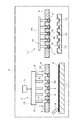
電子部品の1つに、例えば、図8に示すように、両端側にフランジ部53a,53bとを備えたフェライトからなる巻線コア51と、巻線コア51に巻回され、端末がフランジ部53a,53bの下部に配設された電極55に接続されたワイヤ54と、一方側のフランジ部53aから他方側のフランジ部53bにわたるように配設されて一対のフランジ部53a,53bを連結するフェライト板56を備えた構造を有する巻線型コイル部品がある。
For example, as shown in FIG. 8, a winding
そして、このような構造を有する巻線型コイル部品を製造するにあたっては、巻線コア51にワイヤ54を巻回した後、巻線コアの両端側のフランジ部53a,53bの接合面63a,63bにフェライト板56を接着剤57を介して接合することにより製造されている(たとえば特許文献1参照)。
And in manufacturing the winding type coil component which has such a structure, after winding the
なお、この製造方法の場合、電子部品本体である巻線コア51のフェライト板56との接合面63a,63bを、接着剤57に接触させて、該接合面63a,63bに接着剤57を塗布し、巻線コア51の接着剤57が塗布された接合面63a,63bにフェライト板56を押し当てて接着剤57を硬化させることにより、巻線コア51にフェライト板56を接合するようにしている。
In the case of this manufacturing method, the
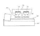
そして、この製造方法においては、巻線コア51の接合面63a,63bに接着剤57を塗布するにあたって、図9に示すように、複数の巻線コア51を一列に並べて収納する、巻線コア51の高さよりも深さが浅い有底の溝71を有し、真空吸引により巻線コア51を溝71内に保持するように構成されたチャック機構70を用い、巻線コア51を溝71に保持した状態で、溝71の開口部を下にし、巻線コア51を下方に突出させた状態でチャック機構70を昇降させることにより、巻線コア51の接合面63a,63bを、塗布テーブル61上に一定厚みに展開された接着剤57に接触させて、巻線コア51の接合面63a,63bに接着剤57を塗布するようにしている。
したがって、巻線コア51は、このチャック機構70の溝71の底部により高さ方向の位置決めがなされた状態で、塗布テーブル61上の接着剤57に接触させられることになる。
And in this manufacturing method, when apply | coating the
Therefore, the
そのため、巻線コア51自体の寸法誤差に加え、チャック機構70の加工精度の誤差により、巻線コア51の接合面63a,63bの高さにばらつきが生じる。この接合面63a,63bの高さ方向のばらつきが許容範囲内にある場合には、接着剤57の塗布が良好に行われるが、巻線コア51の接合面63a,63bが許容範囲を超えて突出したり、突出量が不足したりすると、それが接着剤57の塗布状態のばらつきを招き、組み立て不良を発生する原因になるという問題点がある。
本願発明は、上記課題を解決するものであり、複数の電子部品本体の所定の位置に同時にかつ一様に接着剤を塗布することが可能で、接着剤を介して電子部品本体と被接合部材とが接合された構造を有する電子部品を効率よく製造することが可能な電子部品の製造装置を提供することを目的とする。 The present invention solves the above-described problem, and can apply an adhesive to a predetermined position of a plurality of electronic component main bodies simultaneously and uniformly, and the electronic component main body and the member to be joined via the adhesive. It is an object of the present invention to provide an electronic component manufacturing apparatus capable of efficiently manufacturing an electronic component having a structure in which and are joined.
上記課題を解決するために、請求項1の電子部品の製造装置は、
保持プレートに保持した電子部品本体の接合部に接着剤を塗布し、前記接着剤を介して前記電子部品本体と被接合部材とを接合することにより、前記電子部品本体と被接合部材とが接着剤を介して接合された構造を有する電子部品を製造する電子部品の製造装置であって、
塗布テーブルと、
前記塗布テーブル上に接着剤を一定厚で展開するための接着剤展開手段と、
内周面が弾性材料により構成され、前記内周面により前記電子部品本体を弾性保持する複数の貫通孔が配設された保持プレートと、
前記保持プレートの各貫通孔に対応する位置に、それぞれ独立懸架された状態で配設され、駆動手段により駆動されて、前記貫通孔内に弾性保持された前記電子部品本体を、接着剤を一定厚で展開させた前記塗布テーブルに向かって押圧する押圧ピンを備えた押圧治具と、
前記保持プレートの前記貫通孔に弾性保持された電子部品本体の、前記接着剤が付着した接合部を、前記保持プレートの前記貫通孔に対応する位置に配置された被接合部材に当接させて、前記電子部品本体と前記被接合部材とを接合させる接合機構部と
を具備することを特徴としている。
In order to solve the above-described problem, an electronic component manufacturing apparatus according to
The electronic component main body and the member to be bonded are bonded by applying an adhesive to the joint portion of the electronic component main body held on the holding plate and bonding the electronic component main body and the member to be bonded through the adhesive. An electronic component manufacturing apparatus for manufacturing an electronic component having a structure joined via an agent,
An application table;
An adhesive spreading means for spreading the adhesive on the coating table at a constant thickness;
An inner peripheral surface made of an elastic material, and a holding plate provided with a plurality of through holes for elastically holding the electronic component main body by the inner peripheral surface;
The electronic component main body, which is arranged in a state of being suspended independently from each other in a position corresponding to each through hole of the holding plate and is elastically held in the through hole by being driven by a driving means, is fixed with an adhesive. A pressing jig provided with a pressing pin for pressing toward the coating table developed in thickness;
The joining part of the electronic component main body elastically held in the through hole of the holding plate is attached to a member to be joined disposed at a position corresponding to the through hole of the holding plate. And a joining mechanism portion that joins the electronic component body and the member to be joined.
また、請求項2の電子部品の製造装置は、請求項1の発明の構成において、前記押圧治具が、ゴム状弾性体を用いて形成した基体に、押圧ピンを立設させた構造を有するものであることを特徴としている。 According to a second aspect of the present invention, in the electronic component manufacturing apparatus according to the first aspect of the present invention, the pressing jig has a structure in which a pressing pin is erected on a base formed using a rubber-like elastic body. It is characterized by being.
また、請求項3の電子部品の製造装置は、請求項1または2の発明の構成において、前記押圧治具を構成する前記押圧ピンとして、長さが収縮する方向に応力が加わった場合に、元の長さに戻ろうとする復元力が働くように配設されたバネを備えた押圧ピンが用いられており、前記電子部品本体を、接着剤を一定厚で展開させた前記塗布テーブルに向かって押圧する際に、前記バネによる付勢力により前記電子部品本体に所定の押圧力が加わるように構成されていることを特徴としている。
Further, in the electronic component manufacturing apparatus according to
また、請求項4の電子部品の製造装置は、請求項1〜3のいずれかの発明の構成において、前記接合機構部が、前記保持プレートの上方から、前記貫通孔に弾性保持された前記電子部品本体を下方に押し出す押し出しピンを備えていることを特徴としている。 According to a fourth aspect of the present invention, there is provided the electronic component manufacturing apparatus according to any one of the first to third aspects, wherein the joining mechanism is elastically held in the through hole from above the holding plate. It is characterized by having an extrusion pin that pushes the component body downward.
また、請求項5の電子部品の製造装置は、請求項4の発明の構成において、前記電子部品本体と前記被接合部材とを接合させる際に、前記押し出しピンが、前記電子部品本体の上端面に当接し、前記電子部品本体が前記被接合部材に所定の押圧力をもって当接するように構成されていることを特徴としている。 According to a fifth aspect of the present invention, in the electronic component manufacturing apparatus according to the fourth aspect of the present invention, when the electronic component main body and the member to be bonded are bonded, the push-out pin is an upper end surface of the electronic component main body. The electronic component main body is configured to abut against the member to be joined with a predetermined pressing force.
また、請求項6の電子部品の製造装置は、請求項1〜5のいずれかの発明の構成において、前記接合機構部が、前記保持プレートの貫通孔と略対向する位置に、前記被接合部材が収納保持される複数の有底孔を有する被接合部材収納治具を備えており、前記保持プレートの前記貫通孔に弾性保持された前記電子部品本体のそれぞれが、被接合部材収納治具の有底孔内に収納保持された前記被接合部材のそれぞれと、前記接着剤を介して接合されるように構成されていることを特徴としている。 According to a sixth aspect of the present invention, there is provided the electronic component manufacturing apparatus according to any one of the first to fifth aspects, wherein the joining member is located at a position substantially opposite to the through hole of the holding plate. Each of the electronic component main bodies elastically held in the through-holes of the holding plate is connected to the bonded member storage jig. It is characterized by being configured to be joined to each of the members to be joined housed and held in the bottomed hole via the adhesive.
また、請求項7の電子部品の製造装置は、請求項1〜6のいずれかの発明の構成において、前記電子部品が、ワイヤが巻回された巻線コアの所定の位置にフェライト部材が接合された構造を有する巻線型コイル部品であることを特徴としている。 According to a seventh aspect of the present invention, there is provided the electronic component manufacturing apparatus according to any one of the first to sixth aspects, wherein the electronic component is joined to a predetermined position of the winding core around which the wire is wound. It is a wire-wound coil component having the above-described structure.
請求項1の電子部品の製造装置は、塗布テーブルと、塗布テーブル上に接着剤を一定厚で展開するための接着剤展開手段と、内周面が弾性材料により構成され、内周面により電子部品本体を弾性保持する複数の貫通孔が配設された保持プレートと、保持プレートの各貫通孔に対応する位置に、それぞれ独立懸架された状態で配設され、駆動手段により駆動されて、貫通孔内に弾性保持された電子部品本体を、接着剤を一定厚で展開させた塗布テーブルに向かって押圧する押圧ピンを備えた押圧治具と、保持プレートの貫通孔に弾性保持された電子部品本体の、接着剤が付着した接合部を、保持プレートの貫通孔に対応する位置に配置された被接合部材に当接させて、電子部品本体と被接合部材とを接合させる接合機構部とを備えた構成を有しているので、複数の電子部品本体を保持プレートの貫通孔に保持し、押圧ピンで背後から押圧することにより、各電子部品本体を接着剤が展開された塗布テーブルにほぼ均一な押圧力をもって当接させ、電子部品本体に接着剤を一様に塗布することが可能になり、接合面に一様に接着剤が確実に付着した電子部品本体を被接合部材に当接させることにより、電子部品本体と被接合部材とを確実に接合させることが可能になり、電子部品本体と被接合部材とが接着剤を介して接合された構造を有する電子部品を効率よく製造することが可能になる。 According to another aspect of the invention, there is provided an electronic component manufacturing apparatus comprising: an application table; an adhesive developing means for developing an adhesive on the application table with a constant thickness; and an inner peripheral surface made of an elastic material. A holding plate provided with a plurality of through-holes for elastically holding the component body, and arranged in a state of being suspended independently at positions corresponding to the through-holes of the holding plate, driven by driving means, and passed through. A pressing jig provided with a pressing pin that presses the electronic component main body elastically held in the hole toward the coating table in which the adhesive is spread at a constant thickness, and the electronic component elastically held in the through hole of the holding plate A joining mechanism portion for joining the electronic component body and the joined member by bringing the joined portion of the main body into contact with the joined member arranged at a position corresponding to the through hole of the holding plate. It has a configuration with Therefore, by holding multiple electronic component bodies in the through holes of the holding plate and pressing them from the back with the pressing pins, each electronic component body is brought into contact with the coating table on which the adhesive is spread with a substantially uniform pressing force. The electronic component main body can be applied uniformly to the electronic component main body, and the electronic component main body with the adhesive uniformly adhered to the joining surface is brought into contact with the member to be joined. And the member to be joined can be reliably joined, and an electronic component having a structure in which the electronic component main body and the member to be joined are joined via an adhesive can be efficiently manufactured.
すなわち、本願発明においては、電子部品本体の接合部に接着剤を塗布するにあたって、複数の電子部品本体を保持プレートに設けられた複数の貫通孔の内周面で弾性保持し、かつ独立懸架の押圧ピンで背後から押圧するようにしているので、貫通孔に保持された時点で電子部品本体間に多少の位置ずれがある場合や、保持プレートや各電子部品本体に寸法ばらつきがある場合などにおいても、押圧ピンにより、各電子部品本体の接合部を接着剤層が展開された塗布テーブルにほぼ均一な押圧力をもって当接させることが可能になり、全ての電子部品本体に一様に接着剤を塗布することが可能になる。 That is, in the present invention, when applying the adhesive to the joint portion of the electronic component main body, the plurality of electronic component main bodies are elastically held by the inner peripheral surfaces of the plurality of through holes provided in the holding plate, and are independently suspended. Since it is pressed from behind with a pressing pin, when there is a slight misalignment between the electronic component bodies when they are held in the through holes, or when there are dimensional variations in the holding plate and each electronic component body In addition, the pressing pin makes it possible to bring the joint portion of each electronic component body into contact with the application table on which the adhesive layer is spread with a substantially uniform pressing force, and uniformly adheres to all the electronic component bodies. Can be applied.
その結果、例えば、ワイヤが巻回された巻線コア(電子部品本体)の所定の位置に、フェライト部材(被接合部材)が接着剤を介して接合された構造を有する巻線型コイル部品などの電子部品を製造する場合に、確実にしかも効率よく上述のように構成された電子部品を製造することが可能になる。 As a result, for example, a wound-type coil component having a structure in which a ferrite member (member to be bonded) is bonded to a predetermined position of a winding core (electronic component main body) wound with a wire via an adhesive When manufacturing an electronic component, it is possible to manufacture the electronic component configured as described above reliably and efficiently.
なお、本願発明において、押圧ピンに関し、「独立懸架された状態で配設され」とは、各貫通孔に対応する押圧ピンのそれぞれが、対応する貫通孔に弾性保持された電子部品本体を、所定の押圧力で、接着剤を展開させた塗布テーブルに互いに独立して押圧することができるように配設されていることを意味する概念であり、以下に述べるように、
(a)ゴム状弾性体を用いて形成した基体に、単一または複数の押圧ピンを立設させた構造を有するものや、
(b)押圧ピンの長さが収縮する方向に応力が加わった場合に、元の長さに戻ろうとする復元力が働くように配設されたバネを備えた構造を有するもの
などが、本願発明における、押圧ピンが独立懸架された状態で配設された構成の例として挙げられる。
In the present invention, regarding the pressing pin, `` arranged in an independently suspended state '' means that each of the pressing pins corresponding to each through hole is an electronic component body elastically held in the corresponding through hole, It is a concept that means that it is arranged so that it can be pressed independently from each other on the application table where the adhesive is developed with a predetermined pressing force, as described below,
(a) having a structure in which a single or a plurality of pressing pins are erected on a base formed using a rubber-like elastic body;
(b) When the stress is applied in the direction in which the length of the pressing pin contracts, the one having a structure provided with a spring arranged so that a restoring force to return to the original length is applied. In the invention, an example of a configuration in which the pressing pins are arranged in an independently suspended state is given.
また、請求項2の電子部品の製造装置のように、請求項1の発明の構成において、電子部品本体を押圧する押圧治具として、ゴム状弾性体を用いて形成した基体に、押圧ピンを立設させた構造を有するものを用いるようにした場合、各電子部品本体を押圧する際の、各電子部品本体への押圧力のばらつきを抑制して、各電子部品本体の接合部を、接着剤を一定厚で展開させた塗布テーブルに均一な押圧力で当接させることが可能になり、さらに確実に、保持プレートに保持された複数の電子部品本体のそれぞれに一様に接着剤を塗布することができるようになる。
Further, as in the electronic component manufacturing apparatus according to
また、請求項3の電子部品の製造装置のように、請求項1または2の発明の構成において、押圧治具を構成する押圧ピンとして、長さが収縮する方向に応力が加わった場合に、元の長さに戻ろうとする復元力が働くように配設されたバネを備えた押圧ピンを用いるようにした場合、電子部品本体を、接着剤を一定厚で展開させた塗布テーブルに向かって押圧する際に、バネによる付勢力により電子部品本体を所定の押圧力をもって押圧することが可能になり、各電子部品本体の接合部を、接着剤層が展開された塗布テーブルに均一な押圧力で当接させて、保持プレートに保持された複数の電子部品本体のそれぞれに、さらに確実に、一様に接着剤を塗布することができるようになり、本願発明をより実効あらしめることができる。
Further, as in the electronic component manufacturing apparatus according to
また、請求項4の電子部品の製造装置は、請求項1〜3のいずれかの発明の構成において、接合機構部が、保持プレートの上方から、貫通孔に弾性保持された電子部品本体を下方に押し出す押し出しピンを備えた構成とすることにより、例えば、電子部品本体と被接合部材とを接合させる際に電子部品本体を被接合部に押し付けて電子部品本体と被接合部材との接合をより確実に行うことができるようにしたり、電子部品本体と被接合部材とを接合させた後に、電子部品本体を下方に押し出し、電子部品本体と保持プレートの貫通孔との係合を解除させて次工程に送ったりすることが可能になり、本願発明をさらに実効あらしめることができる。 According to a fourth aspect of the present invention, there is provided the electronic component manufacturing apparatus according to any one of the first to third aspects of the present invention, wherein the joining mechanism portion lowers the electronic component main body elastically held in the through hole from above the holding plate. For example, when the electronic component main body and the member to be bonded are bonded, the electronic component main body is pressed against the bonded portion to bond the electronic component main body and the bonded member more. After the electronic component main body and the member to be joined are bonded, the electronic component main body is pushed downward to release the engagement between the electronic component main body and the through hole of the holding plate. It becomes possible to send it to a process, and the present invention can be further effectively presented.
なお、押し出しピンにより、保持プレートの貫通孔に弾性保持された電子部品本体を下方に押し出す場合、保持プレートを移動させることなく押し出しピンを押し下げるようにしてもよく、また、押し出しピンを移動させることなく保持プレートを上昇させるようにしてもよい。また、保持プレートと押し出しピンの両方を上下方向に移動させるように構成することも可能である。 When the electronic component main body elastically held in the through hole of the holding plate is pushed downward by the push pin, the push pin may be pushed down without moving the hold plate, or the push pin is moved. Alternatively, the holding plate may be raised. It is also possible to configure so that both the holding plate and the push pin are moved in the vertical direction.
また、請求項5の電子部品の製造装置のように、請求項4の発明の構成において、電子部品本体と被接合部材とを接合させる際に、押し出しピンが、電子部品本体の上端面に当接し、電子部品本体が被接合部材に所定の押圧力をもって当接するように構成した場合、電子部品本体と被接合部材とをより確実に接合させることが可能になり、信頼性の高い電子部品をより確実に製造することが可能になる。 Further, as in the electronic component manufacturing apparatus according to the fifth aspect, in the configuration of the invention according to the fourth aspect, when the electronic component main body and the member to be bonded are bonded, the push pin contacts the upper end surface of the electronic component main body. If the electronic component main body is configured to contact the member to be bonded with a predetermined pressing force, the electronic component main body and the member to be bonded can be more reliably bonded, and a highly reliable electronic component can be obtained. It becomes possible to manufacture more reliably.
また、請求項6の電子部品の製造装置のように、請求項1〜5のいずれかの発明の構成において、接合機構部を、保持プレートの貫通孔と略対向する位置に、被接合部材が収納保持される複数の有底孔を有する被接合部材収納治具を備えており、保持プレートの貫通孔に弾性保持された各電子部品本体が、被接合部材収納治具の有底孔内に収納保持された各被接合部材と、接着剤を介して接合されるように構成した場合、複数個の電子部品本体のそれぞれを、対応する位置に保持された被接合部材に効率よくしかも確実に接合させることが可能になり、本願発明をさらに実効あらしめることができる。 Further, as in the electronic component manufacturing apparatus according to the sixth aspect, in the configuration of any one of the first to fifth aspects, the joining member is disposed at a position substantially opposite to the through hole of the holding plate. Each of the electronic component main bodies elastically held in the through holes of the holding plate is provided in the bottomed hole of the bonded member storage jig. When configured to be joined to each member to be joined that is stored and held via an adhesive, each of the plurality of electronic component bodies is efficiently and reliably attached to the member to be joined held at the corresponding position. It becomes possible to make it join, and this invention can be made more effective.
また、本願発明は、請求項7のように、ワイヤが巻回された巻線コアの所定の位置にフェライト部材を接合した構造を有する巻線型コイル部品を製造する場合に、巻線コアの所定の位置にフェライト部材を確実に接合して、上記構成を有する巻線型コイル部品を効率よくしかも確実に製造することが可能になり特に有意義である。 Further, according to the present invention, when manufacturing a wound type coil component having a structure in which a ferrite member is bonded to a predetermined position of a winding core around which a wire is wound, It is particularly significant that the ferrite member is securely joined to the position of the wire-type coil component, and the wire-wound coil component having the above-described configuration can be manufactured efficiently and reliably.
以下に本願発明の実施例を示して、本願発明の特徴とするところをさらに詳しく説明する。 The features of the present invention will be described in more detail below with reference to examples of the present invention.
図1は本願発明の一実施例にかかる電子部品の製造装置の構成を模式的に示す図である。また、図2は、本願発明の一実施例にかかる電子部品の製造装置を用いて製造される電子部品(巻線型コイル部品)の構成を示す図である。 FIG. 1 is a diagram schematically showing the configuration of an electronic component manufacturing apparatus according to an embodiment of the present invention. FIG. 2 is a diagram showing the configuration of an electronic component (winding coil component) manufactured using the electronic component manufacturing apparatus according to one embodiment of the present invention.
この電子部品(巻線型コイル部品)は、図2に示すように、フェライトからなる巻線コア(電子部品本体)4と、巻線コア4の両端側に配設されたフランジ部23a,23bと、巻線コア4に巻回され、端末がフランジ部23a,23bの下部に配設された電極25に接続されたワイヤ24と、一方側のフランジ部23aから他方側のフランジ部23bにわたるように配設されて一対のフランジ部23a,23bを連結するフェライト板(被接合部材)10を備えている。
As shown in FIG. 2, the electronic component (winding coil component) includes a winding core (electronic component body) 4 made of ferrite, and
そして、この巻線型コイル部品においては、フェライト板10とフランジ部23a,23bが接着剤2により接着され、巻線コア4にワイヤ24を巻回した巻線部30には、実質的に接着剤2が塗布されていない構造を有している。
この実施例の電子部品の製造装置Aは、上記巻線型コイル部品を製造するのに用いられるものであって、ワイヤ24が巻回された巻線コア(電子部品本体)4の所定の位置に、フェライト部材(被接合部材)10を接合する工程に用いられるものである。
すなわち、この実施例の電子部品の製造装置Aは、図1に示すように、塗布テーブル1と、塗布テーブル1上に接着剤2を一定厚で展開するための接着剤展開手段であるスキージ3と、巻線コア4を弾性保持する複数の貫通孔5を備えた保持プレート6と、保持プレート6の各貫通孔5に対応する位置に、それぞれ独立懸架された状態で配設され、駆動手段7により駆動されて、貫通孔5内に弾性保持された巻線コア4を、塗布テーブル1に向かって押圧する押圧ピン8を備えた押圧治具9と、巻線コア4の接着剤2が付着した接合部(接合面)4aを、保持プレート6の貫通孔5に対応する位置に配置された被接合部材であるフェライト部材(フェライト板)10に当接させて、巻線コア4とフェライト板10とを接合させるための接合機構部11とを備えている。
In this winding type coil component, the
The electronic component manufacturing apparatus A of this embodiment is used for manufacturing the above-described coiled coil component, and is provided at a predetermined position of a winding core (electronic component main body) 4 around which a
That is, the electronic component manufacturing apparatus A of this embodiment, as shown in FIG. 1, has a coating table 1 and a
また、保持プレート6は貫通孔5の内周面12が弾性材料により構成され、内周面12により、電子部品本体である巻線コア4が弾性保持されるように構成されている。
The holding
さらに、押圧治具9は、図1および図3に示すように、ゴム状弾性体を用いて形成した基体13に、基部18を介して、押圧ピン8を立設することにより構成されている。
Further, as shown in FIGS. 1 and 3, the pressing jig 9 is configured by erecting a
また、押圧ピン8としては、図4(a),(b)に示すように、筒状本体8aと、長さが収縮する方向に応力が加わった場合(図4(a)参照)に、元の長さ(図4(b)参照)に戻ろうとする復元力が働くようなバネ8bを備えた押圧ピンが用いられており、巻線コア4を、接着剤2を一定厚で展開させた塗布テーブル1に向かって押圧する際に、バネ8bによる付勢力により巻線コア4に所定の押圧力が加わるように構成されている。
As shown in FIGS. 4 (a) and 4 (b), as the
また、上記接合機構部11は、図1に示すように、保持プレート6の上方から、貫通孔5に弾性保持された巻線コア4を下方に押し出す押し出しピン14と、押し出しピン14を保持する押し出しピン用基体15を備えている。
なお、この実施例では、押し出しピン14を、保持プレート6の貫通孔5に弾性保持させた巻線コア4の上面に当接させた状態で、保持プレート6を上方に移動させることにより、貫通孔5に弾性保持された巻線コア4が貫通孔5から押し出され、保持プレート6による巻線コア4の保持が解除されるように構成されている。
Further, as shown in FIG. 1, the joining
In this embodiment, the extruding
また、この実施例の電子部品の製造装置Aにおいては、巻線コア4と、フェライト板10とを接合させる際に、押し出しピン14が、巻線コア4の上端面に当接し、巻線コア4がフェライト板10に所定の押圧力をもって当接するように構成されている。
In addition, in the electronic component manufacturing apparatus A of this embodiment, when the winding
さらに、この実施例の電子部品の製造装置Aにおいては、接合機構部11が、保持プレート6の貫通孔5と略対向する位置に、被接合部材であるフェライト10が収納保持される複数の有底孔16を有する板状の被接合部材収納治具17を備えており、保持プレート6と被接合部材収納治具17のいずれか一方、あるいは、両方を相手側に向かって移動させることにより、保持プレート6の複数の貫通孔5に弾性保持された各巻線コア4が、被接合部材収納治具17の複数の有底孔16内に収納保持された各フェライト板10と、接着剤2を介して接合されるように構成されている。
なお、特に図示しないが、被接合部材収納治具17の有底孔16の底部には、フェライト板10が接合された後の巻線コア4を取り出すための取り出しピンを挿入するための挿入孔が配設されている。
Furthermore, in the electronic device manufacturing apparatus A of this embodiment, the
Although not particularly illustrated, an insertion hole for inserting a take-out pin for taking out the winding
次に、上述のように構成された電子部品の製造装置Aを用いて、図2に示すように、ワイヤ24が巻回された巻線コア(電子部品本体)4の所定の位置に、フェライト板(被接合部材)10が接合された構造を有する巻線型コイル部品を製造する方法について説明する。
Next, as shown in FIG. 2, the electronic component manufacturing apparatus A configured as described above is used to place ferrite at a predetermined position of the winding core (electronic component main body) 4 around which the
(1)まず、所定の工程から搬送されてきた、貫通孔5に巻線コア4が保持された保持プレート6を受け取り、巻線コア4の、フェライト板10との接合面4aが保持プレート6の下面側から僅かに下方に突出するように押圧治具9の押圧ピン8により押圧する。
(1) First, the holding
(2)それから、搬送機構(図示せず)により、保持プレート6を、図1に示すように、巻線コア4の接合面4aに接着剤2を塗布するための位置、すなわち、塗布テーブル1の上方の位置に搬送する。
なお、保持プレート6が搬送されるまでの間に、スキージ3により接着剤2を、塗布テーブル1上に一定厚となるように展開し、接着剤を塗布する準備をしておく。
(2) Then, as shown in FIG. 1, the position for applying the adhesive 2 to the
Before the holding
(3)それから、図5に示すように、塗布テーブル1上に、わずかに浮かせて保持プレート6を位置させ、保持プレート6の上面(背面)から、押圧ピン8を貫通孔5に挿入し、個別に巻線コア4を押圧して、巻線コア4の接合面4aを、一定厚で接着剤2を展開させた塗布テーブル1の表面に押し付ける。
(3) Then, as shown in FIG. 5, the holding
(4)そして、接着剤2を塗布した巻線コア4を、保持プレート6の貫通孔5に保持させたまま、巻線コア4とフェライト板10を接合させるべき領域に搬送する(図1)。
このとき、貫通孔5に弾性保持された各巻線コア4が、接合機構部11を構成する被接合部材収納治具17の、複数の有底孔16内に収納保持された各フェライト板10の上方に位置するようにする。
(4) Then, the winding
At this time, the winding
(5)そして、図6に示すように、保持プレート6の貫通孔5と、被接合部材収納治具17の有底孔16とが互いに対向するように位置決めされた状態で、保持プレート6の上面側から、押し出しピン14を挿入し、貫通孔5内の巻線コア4をフェライト板10に押し付ける。
(5) Then, as shown in FIG. 6, in a state where the through
(6)その後、図7に示すように、押し出しピン14により、巻線コア4をフェライト板10に所定の押圧力で押圧した状態で、保持プレート6のみを上昇させ、被接合部材収納治具17の有底孔16内にフェライト板10が接合された巻線コア4が載置された状態とする。
(6) Thereafter, as shown in FIG. 7, only the holding
(7)次いで、フェライト板10が接合された巻線コア4を、被接合部材収納治具17ごと、接着剤2を硬化させるための領域(例えば、加熱手段を備えた熱処理装置)に搬送し、接着剤2を硬化させる。
(7) Next, the winding
(8)それから、接着剤2が硬化し、フェライト板10が固着された巻線コア4(すなわち製品である巻線型コイル部品)を、被接合部材収納治具17上に保持したまま部品排出領域に搬送し、被接合部材収納治具17の有底孔16の底部に形成された挿入孔(図示せず)から、取り出しピン(図示せず)を挿入し、製品である巻線型コイル部品を取り出す。
(8) Then, the
上記実施例では、巻線コア(電子部品本体)4の接合面4aに接着剤2を塗布するにあたって、複数の巻線コア(電子部品本体)4を保持プレート6に設けられた複数の貫通孔5の内周面で弾性保持し、かつ独立懸架の押圧ピン8で背後から押圧するようにしているので、貫通孔5に弾性保持された時点で各巻線コア(電子部品本体)4間に多少の位置ずれがあるような場合や、保持プレート6や各巻線コア(電子部品本体)4に寸法ばらつきがあるような場合にも、押圧ピン8により、各巻線コア(電子部品本体)4の接合面4aを接着剤2が展開された塗布テーブル1にほぼ均一な押圧力をもって当接させることが可能になり、複数の巻線コア(電子部品本体)4に一様に接着剤2を塗布することが可能になる。
In the above embodiment, when the adhesive 2 is applied to the
なお、具体的には、上述の特許文献1の方法では、接着剤2の塗布不良率が0.1〜0.2%であったものを、上記実施例の方法では実質的に塗布不良率が0%となるようにすることができることを確認している。
Specifically, in the method of
したがって、上記実施例の製造方法によれば、ワイヤ24が巻回された巻線コア(電子部品本体)4の接合面4aに、フェライト部材(被接合部材)10が接着剤2を介して接合された構造を有する巻線型コイル部品(電子部品)を確実にしかも効率よく製造することができる。
Therefore, according to the manufacturing method of the above embodiment, the ferrite member (member to be joined) 10 is joined via the adhesive 2 to the joining
なお、上記実施例では、巻線型コイル部品を製造する場合を例にとって説明したが、本願発明を適用することにより、巻線型コイル部品に限らず、電子部品本体と被接合部材とが接着剤を介して接合された構造を有する電子部品(例えば、保護ケース付き電子部品(ケースと電子部品本体とを接着するもの))などを効率よく製造することができる。 In the above embodiment, the case of manufacturing a wound coil component has been described as an example. However, by applying the present invention, not only the wound coil component but also the electronic component main body and the member to be joined have an adhesive. Thus, it is possible to efficiently manufacture an electronic component (for example, an electronic component with a protective case (that adheres the case and the electronic component main body)) having a structure joined through the two.
また、上記実施例では、押圧治具9として、ゴム状弾性体を用いて形成した基体13に、長さが収縮する方向に応力が加わった場合に、元の長さに戻ろうとする復元力が働くバネ8bを備えた押圧ピン8を立設することにより形成された押圧治具を用いているが、この実施例のように、ゴム状弾性体からなる基体13を用いた場合には、上述のようなバネを備えていない、剛性を有する材料からなる押圧ピンを用いることも可能であり、また、上記のようにバネを備えた押圧ピン8を用いた場合には、基体13として、金属などの剛体からなる基体を用いることも可能である。
Moreover, in the said Example, when the stress is applied to the base |
本願発明はさらにその他の点においても上記実施例に限定されるものではなく、保持プレートの具体的な構造、保持プレートに配設される貫通孔の配設数や配設位置、貫通孔の具体的な形状、貫通孔の内周面を構成する材料の種類、接合機構部を構成する押し出しピンの具体的な形状、接合機構部が備える、被接合部材収納治具やそれに配設される有底孔の具体的な構造などに関し、発明の範囲内において、種々の応用、変形を加えることが可能である。 The invention of the present application is not limited to the above embodiment in other points as well. The specific structure of the holding plate, the number and positions of the through holes provided in the holding plate, and the specifics of the through holes. Shape, the type of material constituting the inner peripheral surface of the through-hole, the specific shape of the push pin constituting the joining mechanism, the member to be joined storage jig provided in the joining mechanism, and the With respect to the specific structure of the bottom hole, various applications and modifications can be made within the scope of the invention.
上述のように、本願発明によれば、電子部品本体を保持プレートに設けられた複数の貫通孔の内周面で弾性保持し、かつ独立懸架の押圧ピンで背後から押圧するようにしているので、貫通孔に弾性保持された時点で電子部品本体間に多少の位置ずれがある場合や、保持プレートや電子部品本体に寸法ばらつきがあるような場合にも、押圧ピンにより、電子部品本体の接合面を接着剤にほぼ均一な押圧力をもって当接させることが可能になり、電子部品本体に接着剤を介して被接合部材が接合された構造を有する電子部品を効率よく製造することができる。
したがって、本願発明は、例えば、巻線コアなどの電子部品本体の接合面に、フェライト部材などの被接合部材が接着剤を介して接合された構造を有する巻線型コイル部品などの電子部品を製造する場合に広く適用することが可能である。
As described above, according to the present invention, the electronic component main body is elastically held by the inner peripheral surfaces of the plurality of through holes provided in the holding plate, and is pressed from behind by the independent suspension pressing pins. Even when there is a slight misalignment between the electronic component bodies when they are elastically held in the through holes, or when there is a dimensional variation in the holding plate or electronic component body, The surface can be brought into contact with the adhesive with a substantially uniform pressing force, and an electronic component having a structure in which a member to be bonded is bonded to the electronic component main body via the adhesive can be efficiently manufactured.
Therefore, the present invention manufactures an electronic component such as a wound coil component having a structure in which a bonded member such as a ferrite member is bonded to the bonding surface of an electronic component main body such as a winding core via an adhesive. It is possible to apply widely when doing.
A 電子部品の製造装置
1 塗布テーブル
2 接着剤
3 スキージ
4 巻線コア(電子部品本体)
4a 接合部(接合面)
5 貫通孔
6 保持プレート
7 駆動手段
8 押圧ピン
8a 筒状本体
8b バネ
9 押圧治具
10 フェライト板(フェライト部材、被接合部材)
11 接合機構部
12 貫通孔の内周面
13 基体
14 押し出しピン
15 押し出しピン用基体
16 有底孔
17 被接合部材収納治具
18 基部
23a,23b フランジ部
24 ワイヤ
25 電極
30 巻線部
A Electronic
4a Joint (joint surface)
DESCRIPTION OF
DESCRIPTION OF
Claims (7)
塗布テーブルと、
前記塗布テーブル上に接着剤を一定厚で展開するための接着剤展開手段と、
内周面が弾性材料により構成され、前記内周面により前記電子部品本体を弾性保持する複数の貫通孔が配設された保持プレートと、
前記保持プレートの各貫通孔に対応する位置に、それぞれ独立懸架された状態で配設され、駆動手段により駆動されて、前記貫通孔内に弾性保持された前記電子部品本体を、接着剤を一定厚で展開させた前記塗布テーブルに向かって押圧する押圧ピンを備えた押圧治具と、
前記保持プレートの前記貫通孔に弾性保持された電子部品本体の、前記接着剤が付着した接合部を、前記保持プレートの前記貫通孔に対応する位置に配置された被接合部材に当接させて、前記電子部品本体と前記被接合部材とを接合させる接合機構部と
を具備することを特徴とする電子部品の製造装置。 The electronic component main body and the member to be bonded are bonded by applying an adhesive to the joint portion of the electronic component main body held on the holding plate and bonding the electronic component main body and the member to be bonded through the adhesive. An electronic component manufacturing apparatus for manufacturing an electronic component having a structure joined via an agent,
An application table;
An adhesive spreading means for spreading the adhesive on the coating table at a constant thickness;
An inner peripheral surface made of an elastic material, and a holding plate provided with a plurality of through holes for elastically holding the electronic component main body by the inner peripheral surface;
The electronic component main body, which is arranged in a state of being suspended independently from each other in a position corresponding to each through hole of the holding plate and is elastically held in the through hole by being driven by a driving means, is fixed with an adhesive. A pressing jig provided with a pressing pin for pressing toward the coating table developed in thickness;
The joining part of the electronic component main body elastically held in the through hole of the holding plate is attached to a member to be joined disposed at a position corresponding to the through hole of the holding plate. An electronic component manufacturing apparatus comprising: a joining mechanism unit that joins the electronic component body and the member to be joined.
Priority Applications (1)
| Application Number | Priority Date | Filing Date | Title |
|---|---|---|---|
| JP2006041435A JP4779693B2 (en) | 2006-02-17 | 2006-02-17 | Electronic component manufacturing equipment |
Applications Claiming Priority (1)
| Application Number | Priority Date | Filing Date | Title |
|---|---|---|---|
| JP2006041435A JP4779693B2 (en) | 2006-02-17 | 2006-02-17 | Electronic component manufacturing equipment |
Publications (2)
| Publication Number | Publication Date |
|---|---|
| JP2007221002A true JP2007221002A (en) | 2007-08-30 |
| JP4779693B2 JP4779693B2 (en) | 2011-09-28 |
Family
ID=38497925
Family Applications (1)
| Application Number | Title | Priority Date | Filing Date |
|---|---|---|---|
| JP2006041435A Active JP4779693B2 (en) | 2006-02-17 | 2006-02-17 | Electronic component manufacturing equipment |
Country Status (1)
| Country | Link |
|---|---|
| JP (1) | JP4779693B2 (en) |
Citations (3)
| Publication number | Priority date | Publication date | Assignee | Title |
|---|---|---|---|---|
| JPH06176992A (en) * | 1992-12-04 | 1994-06-24 | Murata Mfg Co Ltd | Electrode formation system of chip component |
| JPH0922854A (en) * | 1995-07-07 | 1997-01-21 | Taiyo Yuden Co Ltd | External electrode formation method for electronic parts |
| JP2003086442A (en) * | 2001-09-12 | 2003-03-20 | Murata Mfg Co Ltd | Method for manufacturing wound coil component and coil component |
-
2006
- 2006-02-17 JP JP2006041435A patent/JP4779693B2/en active Active
Patent Citations (3)
| Publication number | Priority date | Publication date | Assignee | Title |
|---|---|---|---|---|
| JPH06176992A (en) * | 1992-12-04 | 1994-06-24 | Murata Mfg Co Ltd | Electrode formation system of chip component |
| JPH0922854A (en) * | 1995-07-07 | 1997-01-21 | Taiyo Yuden Co Ltd | External electrode formation method for electronic parts |
| JP2003086442A (en) * | 2001-09-12 | 2003-03-20 | Murata Mfg Co Ltd | Method for manufacturing wound coil component and coil component |
Also Published As
| Publication number | Publication date |
|---|---|
| JP4779693B2 (en) | 2011-09-28 |
Similar Documents
| Publication | Publication Date | Title |
|---|---|---|
| JP2682250B2 (en) | Electronic component chip holder and electronic component chip handling method | |
| US11217389B2 (en) | Method and apparatus for manufacturing coil component | |
| US10395824B2 (en) | Method of manufacturing winding-type coil component | |
| JP2001118755A (en) | Holder for chip component and method for handling chip component | |
| JPWO2016027659A1 (en) | Method for manufacturing wire-wound coil component | |
| JP4779693B2 (en) | Electronic component manufacturing equipment | |
| KR20030023471A (en) | Manufacturing method of wound coil component, and the coil component | |
| JP2009272446A (en) | Method of manufacturing coil part | |
| US6877542B2 (en) | Systems and methods for bonding a heat sink to a printed circuit assembly | |
| JP5228887B2 (en) | Manufacturing method of electronic parts | |
| KR101524975B1 (en) | Tool for chip-removal | |
| CN110416176B (en) | Semiconductor device and manufacturing method thereof, semiconductor assembly and metal connecting piece | |
| JP6268558B2 (en) | Method for manufacturing wire-wound coil component | |
| KR100959689B1 (en) | A method for forming a electrode | |
| CN110246681B (en) | Method for manufacturing coil component and apparatus for manufacturing coil component | |
| JP5671378B2 (en) | Connector and method for connecting capacitor and terminal metal fitting constituting connector | |
| JP2018115050A (en) | Member affixing apparatus | |
| JPWO2016125763A1 (en) | Mounting apparatus and mounting method | |
| JP2008288324A (en) | Bonding apparatus and bonding method | |
| JP2008016690A (en) | Connection structure for connecting electrode of substrate and connection method | |
| US9566764B1 (en) | Fast cure conductive epoxy attach methodology for high speed automated processes | |
| JPH0464451B2 (en) | ||
| JP2001028315A (en) | Manufacture of high-accuracy thermally stable electromagnetic coil plate | |
| JP2017199805A (en) | Shaking-in jig and method for manufacturing electronic component using the same | |
| JP2014045199A (en) | Bonding apparatus, and bonding method |
Legal Events
| Date | Code | Title | Description |
|---|---|---|---|
| A621 | Written request for application examination |
Free format text: JAPANESE INTERMEDIATE CODE: A621 Effective date: 20081016 |
|
| A131 | Notification of reasons for refusal |
Free format text: JAPANESE INTERMEDIATE CODE: A131 Effective date: 20100928 |
|
| A521 | Written amendment |
Free format text: JAPANESE INTERMEDIATE CODE: A523 Effective date: 20101129 |
|
| TRDD | Decision of grant or rejection written | ||
| A01 | Written decision to grant a patent or to grant a registration (utility model) |
Free format text: JAPANESE INTERMEDIATE CODE: A01 Effective date: 20110607 |
|
| A01 | Written decision to grant a patent or to grant a registration (utility model) |
Free format text: JAPANESE INTERMEDIATE CODE: A01 |
|
| A61 | First payment of annual fees (during grant procedure) |
Free format text: JAPANESE INTERMEDIATE CODE: A61 Effective date: 20110620 |
|
| FPAY | Renewal fee payment (event date is renewal date of database) |
Free format text: PAYMENT UNTIL: 20140715 Year of fee payment: 3 |
|
| R150 | Certificate of patent or registration of utility model |
Free format text: JAPANESE INTERMEDIATE CODE: R150 Ref document number: 4779693 Country of ref document: JP Free format text: JAPANESE INTERMEDIATE CODE: R150 |