JP2007201192A - Organic electroluminescence device - Google Patents
Organic electroluminescence device Download PDFInfo
- Publication number
- JP2007201192A JP2007201192A JP2006018154A JP2006018154A JP2007201192A JP 2007201192 A JP2007201192 A JP 2007201192A JP 2006018154 A JP2006018154 A JP 2006018154A JP 2006018154 A JP2006018154 A JP 2006018154A JP 2007201192 A JP2007201192 A JP 2007201192A
- Authority
- JP
- Japan
- Prior art keywords
- charge transporting
- light emitting
- emitting layer
- transition
- light
- Prior art date
- Legal status (The legal status is an assumption and is not a legal conclusion. Google has not performed a legal analysis and makes no representation as to the accuracy of the status listed.)
- Pending
Links
- 238000005401 electroluminescence Methods 0.000 title abstract description 12
- 229920000570 polyether Polymers 0.000 claims abstract description 115
- 239000004721 Polyphenylene oxide Substances 0.000 claims abstract description 100
- 230000007704 transition Effects 0.000 claims abstract description 54
- 150000002894 organic compounds Chemical class 0.000 claims abstract description 47
- 125000000217 alkyl group Chemical group 0.000 claims abstract description 19
- 125000003118 aryl group Chemical group 0.000 claims abstract description 17
- 125000004435 hydrogen atom Chemical group [H]* 0.000 claims abstract description 15
- 239000004215 Carbon black (E152) Substances 0.000 claims abstract description 14
- 229930195733 hydrocarbon Natural products 0.000 claims abstract description 14
- 150000002430 hydrocarbons Chemical class 0.000 claims abstract description 14
- 125000003545 alkoxy group Chemical group 0.000 claims abstract description 9
- 239000000463 material Substances 0.000 claims description 152
- 230000005283 ground state Effects 0.000 claims description 52
- 150000003384 small molecules Chemical class 0.000 claims description 51
- 230000005525 hole transport Effects 0.000 claims description 49
- 238000002347 injection Methods 0.000 claims description 39
- 239000007924 injection Substances 0.000 claims description 39
- 125000004432 carbon atom Chemical group C* 0.000 claims description 20
- 125000003710 aryl alkyl group Chemical group 0.000 claims description 10
- OKTJSMMVPCPJKN-UHFFFAOYSA-N Carbon Chemical group [C] OKTJSMMVPCPJKN-UHFFFAOYSA-N 0.000 claims description 4
- 229910052799 carbon Inorganic materials 0.000 claims description 4
- 230000005284 excitation Effects 0.000 abstract description 3
- 230000003252 repetitive effect Effects 0.000 abstract 1
- 239000010410 layer Substances 0.000 description 240
- 150000001875 compounds Chemical class 0.000 description 65
- 239000002904 solvent Substances 0.000 description 64
- YXFVVABEGXRONW-UHFFFAOYSA-N Toluene Chemical compound CC1=CC=CC=C1 YXFVVABEGXRONW-UHFFFAOYSA-N 0.000 description 42
- 239000000243 solution Substances 0.000 description 36
- 239000010408 film Substances 0.000 description 33
- 238000006243 chemical reaction Methods 0.000 description 31
- 238000000034 method Methods 0.000 description 31
- MVPPADPHJFYWMZ-UHFFFAOYSA-N chlorobenzene Chemical compound ClC1=CC=CC=C1 MVPPADPHJFYWMZ-UHFFFAOYSA-N 0.000 description 30
- 229920000642 polymer Polymers 0.000 description 30
- UHOVQNZJYSORNB-UHFFFAOYSA-N Benzene Chemical compound C1=CC=CC=C1 UHOVQNZJYSORNB-UHFFFAOYSA-N 0.000 description 24
- 239000000178 monomer Substances 0.000 description 22
- -1 poly (p-phenylene vinylene) Polymers 0.000 description 22
- 238000006116 polymerization reaction Methods 0.000 description 18
- 238000004528 spin coating Methods 0.000 description 18
- 239000000758 substrate Substances 0.000 description 18
- XLYOFNOQVPJJNP-UHFFFAOYSA-N water Substances O XLYOFNOQVPJJNP-UHFFFAOYSA-N 0.000 description 18
- 239000004810 polytetrafluoroethylene Substances 0.000 description 17
- 229920001343 polytetrafluoroethylene Polymers 0.000 description 17
- PPBRXRYQALVLMV-UHFFFAOYSA-N Styrene Chemical compound C=CC1=CC=CC=C1 PPBRXRYQALVLMV-UHFFFAOYSA-N 0.000 description 16
- 238000009835 boiling Methods 0.000 description 16
- YMWUJEATGCHHMB-UHFFFAOYSA-N Dichloromethane Chemical compound ClCCl YMWUJEATGCHHMB-UHFFFAOYSA-N 0.000 description 15
- SCYULBFZEHDVBN-UHFFFAOYSA-N 1,1-Dichloroethane Chemical compound CC(Cl)Cl SCYULBFZEHDVBN-UHFFFAOYSA-N 0.000 description 14
- 238000010549 co-Evaporation Methods 0.000 description 14
- 238000005227 gel permeation chromatography Methods 0.000 description 14
- 239000011521 glass Substances 0.000 description 14
- 125000002887 hydroxy group Chemical group [H]O* 0.000 description 14
- 229910019015 Mg-Ag Inorganic materials 0.000 description 13
- 229910045601 alloy Inorganic materials 0.000 description 13
- 239000000956 alloy Substances 0.000 description 13
- ZMXDDKWLCZADIW-UHFFFAOYSA-N N,N-Dimethylformamide Chemical compound CN(C)C=O ZMXDDKWLCZADIW-UHFFFAOYSA-N 0.000 description 12
- WYURNTSHIVDZCO-UHFFFAOYSA-N Tetrahydrofuran Chemical compound C1CCOC1 WYURNTSHIVDZCO-UHFFFAOYSA-N 0.000 description 12
- ZMANZCXQSJIPKH-UHFFFAOYSA-N Triethylamine Chemical compound CCN(CC)CC ZMANZCXQSJIPKH-UHFFFAOYSA-N 0.000 description 12
- 239000003054 catalyst Substances 0.000 description 10
- 238000005530 etching Methods 0.000 description 9
- 238000001771 vacuum deposition Methods 0.000 description 9
- OCJBOOLMMGQPQU-UHFFFAOYSA-N 1,4-dichlorobenzene Chemical compound ClC1=CC=C(Cl)C=C1 OCJBOOLMMGQPQU-UHFFFAOYSA-N 0.000 description 8
- IAZDPXIOMUYVGZ-UHFFFAOYSA-N Dimethylsulphoxide Chemical compound CS(C)=O IAZDPXIOMUYVGZ-UHFFFAOYSA-N 0.000 description 8
- JUJWROOIHBZHMG-UHFFFAOYSA-N Pyridine Chemical compound C1=CC=NC=C1 JUJWROOIHBZHMG-UHFFFAOYSA-N 0.000 description 8
- 238000000576 coating method Methods 0.000 description 8
- 230000000052 comparative effect Effects 0.000 description 8
- 229940117389 dichlorobenzene Drugs 0.000 description 8
- 238000001035 drying Methods 0.000 description 8
- 238000004519 manufacturing process Methods 0.000 description 8
- LQNUZADURLCDLV-UHFFFAOYSA-N nitrobenzene Chemical compound [O-][N+](=O)C1=CC=CC=C1 LQNUZADURLCDLV-UHFFFAOYSA-N 0.000 description 8
- 239000002861 polymer material Substances 0.000 description 8
- GETQZCLCWQTVFV-UHFFFAOYSA-N trimethylamine Chemical compound CN(C)C GETQZCLCWQTVFV-UHFFFAOYSA-N 0.000 description 8
- 239000002253 acid Substances 0.000 description 7
- 239000006185 dispersion Substances 0.000 description 7
- 239000012212 insulator Substances 0.000 description 7
- 229910052751 metal Inorganic materials 0.000 description 7
- 239000002184 metal Substances 0.000 description 7
- 229920000728 polyester Polymers 0.000 description 7
- JTPNRXUCIXHOKM-UHFFFAOYSA-N 1-chloronaphthalene Chemical compound C1=CC=C2C(Cl)=CC=CC2=C1 JTPNRXUCIXHOKM-UHFFFAOYSA-N 0.000 description 6
- ZWEHNKRNPOVVGH-UHFFFAOYSA-N 2-Butanone Chemical compound CCC(C)=O ZWEHNKRNPOVVGH-UHFFFAOYSA-N 0.000 description 6
- WFDIJRYMOXRFFG-UHFFFAOYSA-N Acetic anhydride Chemical compound CC(=O)OC(C)=O WFDIJRYMOXRFFG-UHFFFAOYSA-N 0.000 description 6
- RTZKZFJDLAIYFH-UHFFFAOYSA-N Diethyl ether Chemical compound CCOCC RTZKZFJDLAIYFH-UHFFFAOYSA-N 0.000 description 6
- OKKJLVBELUTLKV-UHFFFAOYSA-N Methanol Chemical compound OC OKKJLVBELUTLKV-UHFFFAOYSA-N 0.000 description 6
- KWYUFKZDYYNOTN-UHFFFAOYSA-M Potassium hydroxide Chemical compound [OH-].[K+] KWYUFKZDYYNOTN-UHFFFAOYSA-M 0.000 description 6
- HEMHJVSKTPXQMS-UHFFFAOYSA-M Sodium hydroxide Chemical compound [OH-].[Na+] HEMHJVSKTPXQMS-UHFFFAOYSA-M 0.000 description 6
- 239000003960 organic solvent Substances 0.000 description 6
- 125000001997 phenyl group Chemical group [H]C1=C([H])C([H])=C(*)C([H])=C1[H] 0.000 description 6
- 238000001226 reprecipitation Methods 0.000 description 6
- 238000001308 synthesis method Methods 0.000 description 6
- YLQBMQCUIZJEEH-UHFFFAOYSA-N tetrahydrofuran Natural products C=1C=COC=1 YLQBMQCUIZJEEH-UHFFFAOYSA-N 0.000 description 6
- XLJMAIOERFSOGZ-UHFFFAOYSA-N anhydrous cyanic acid Natural products OC#N XLJMAIOERFSOGZ-UHFFFAOYSA-N 0.000 description 5
- 230000018044 dehydration Effects 0.000 description 5
- 238000006297 dehydration reaction Methods 0.000 description 5
- OCKFCYARHPIGDV-UHFFFAOYSA-N tetraphenylene-1,2-diamine Chemical class C1=CC=C2C3=C(N)C(N)=CC=C3C3=CC=CC=C3C3=CC=CC=C3C2=C1 OCKFCYARHPIGDV-UHFFFAOYSA-N 0.000 description 5
- 239000010409 thin film Substances 0.000 description 5
- 238000007740 vapor deposition Methods 0.000 description 5
- CYSGHNMQYZDMIA-UHFFFAOYSA-N 1,3-Dimethyl-2-imidazolidinon Chemical compound CN1CCN(C)C1=O CYSGHNMQYZDMIA-UHFFFAOYSA-N 0.000 description 4
- GSLTVFIVJMCNBH-UHFFFAOYSA-N 2-isocyanatopropane Chemical compound CC(C)N=C=O GSLTVFIVJMCNBH-UHFFFAOYSA-N 0.000 description 4
- CSCPPACGZOOCGX-UHFFFAOYSA-N Acetone Chemical compound CC(C)=O CSCPPACGZOOCGX-UHFFFAOYSA-N 0.000 description 4
- LFQSCWFLJHTTHZ-UHFFFAOYSA-N Ethanol Chemical compound CCO LFQSCWFLJHTTHZ-UHFFFAOYSA-N 0.000 description 4
- VEXZGXHMUGYJMC-UHFFFAOYSA-N Hydrochloric acid Chemical compound Cl VEXZGXHMUGYJMC-UHFFFAOYSA-N 0.000 description 4
- SECXISVLQFMRJM-UHFFFAOYSA-N N-Methylpyrrolidone Chemical compound CN1CCCC1=O SECXISVLQFMRJM-UHFFFAOYSA-N 0.000 description 4
- KEAYESYHFKHZAL-UHFFFAOYSA-N Sodium Chemical compound [Na] KEAYESYHFKHZAL-UHFFFAOYSA-N 0.000 description 4
- QAOWNCQODCNURD-UHFFFAOYSA-N Sulfuric acid Chemical compound OS(O)(=O)=O QAOWNCQODCNURD-UHFFFAOYSA-N 0.000 description 4
- YTPLMLYBLZKORZ-UHFFFAOYSA-N Thiophene Chemical compound C=1C=CSC=1 YTPLMLYBLZKORZ-UHFFFAOYSA-N 0.000 description 4
- DTQVDTLACAAQTR-UHFFFAOYSA-N Trifluoroacetic acid Chemical compound OC(=O)C(F)(F)F DTQVDTLACAAQTR-UHFFFAOYSA-N 0.000 description 4
- 239000003377 acid catalyst Substances 0.000 description 4
- 125000000609 carbazolyl group Chemical group C1(=CC=CC=2C3=CC=CC=C3NC12)* 0.000 description 4
- 239000003795 chemical substances by application Substances 0.000 description 4
- 239000011248 coating agent Substances 0.000 description 4
- 238000009833 condensation Methods 0.000 description 4
- 230000005494 condensation Effects 0.000 description 4
- KQWGXHWJMSMDJJ-UHFFFAOYSA-N cyclohexyl isocyanate Chemical compound O=C=NC1CCCCC1 KQWGXHWJMSMDJJ-UHFFFAOYSA-N 0.000 description 4
- 238000010586 diagram Methods 0.000 description 4
- 150000004820 halides Chemical class 0.000 description 4
- 239000012442 inert solvent Substances 0.000 description 4
- 238000010030 laminating Methods 0.000 description 4
- PSHKMPUSSFXUIA-UHFFFAOYSA-N n,n-dimethylpyridin-2-amine Chemical compound CN(C)C1=CC=CC=N1 PSHKMPUSSFXUIA-UHFFFAOYSA-N 0.000 description 4
- 230000000704 physical effect Effects 0.000 description 4
- BASFCYQUMIYNBI-UHFFFAOYSA-N platinum Chemical compound [Pt] BASFCYQUMIYNBI-UHFFFAOYSA-N 0.000 description 4
- UMJSCPRVCHMLSP-UHFFFAOYSA-N pyridine Natural products COC1=CC=CN=C1 UMJSCPRVCHMLSP-UHFFFAOYSA-N 0.000 description 4
- 229910052761 rare earth metal Inorganic materials 0.000 description 4
- 150000002910 rare earth metals Chemical class 0.000 description 4
- 239000011347 resin Substances 0.000 description 4
- 229920005989 resin Polymers 0.000 description 4
- JOXIMZWYDAKGHI-UHFFFAOYSA-N toluene-4-sulfonic acid Chemical compound CC1=CC=C(S(O)(=O)=O)C=C1 JOXIMZWYDAKGHI-UHFFFAOYSA-N 0.000 description 4
- 229910052723 transition metal Inorganic materials 0.000 description 4
- 150000003624 transition metals Chemical class 0.000 description 4
- JIAARYAFYJHUJI-UHFFFAOYSA-L zinc dichloride Chemical compound [Cl-].[Cl-].[Zn+2] JIAARYAFYJHUJI-UHFFFAOYSA-L 0.000 description 4
- IUVCFHHAEHNCFT-INIZCTEOSA-N 2-[(1s)-1-[4-amino-3-(3-fluoro-4-propan-2-yloxyphenyl)pyrazolo[3,4-d]pyrimidin-1-yl]ethyl]-6-fluoro-3-(3-fluorophenyl)chromen-4-one Chemical compound C1=C(F)C(OC(C)C)=CC=C1C(C1=C(N)N=CN=C11)=NN1[C@@H](C)C1=C(C=2C=C(F)C=CC=2)C(=O)C2=CC(F)=CC=C2O1 IUVCFHHAEHNCFT-INIZCTEOSA-N 0.000 description 3
- DDTHMESPCBONDT-UHFFFAOYSA-N 4-(4-oxocyclohexa-2,5-dien-1-ylidene)cyclohexa-2,5-dien-1-one Chemical class C1=CC(=O)C=CC1=C1C=CC(=O)C=C1 DDTHMESPCBONDT-UHFFFAOYSA-N 0.000 description 3
- ZYASLTYCYTYKFC-UHFFFAOYSA-N 9-methylidenefluorene Chemical class C1=CC=C2C(=C)C3=CC=CC=C3C2=C1 ZYASLTYCYTYKFC-UHFFFAOYSA-N 0.000 description 3
- OWIKHYCFFJSOEH-UHFFFAOYSA-N Isocyanic acid Chemical compound N=C=O OWIKHYCFFJSOEH-UHFFFAOYSA-N 0.000 description 3
- 125000004429 atom Chemical group 0.000 description 3
- 150000001716 carbazoles Chemical class 0.000 description 3
- 239000012948 isocyanate Substances 0.000 description 3
- 239000003446 ligand Substances 0.000 description 3
- SMBBZHGTZJNSRQ-UHFFFAOYSA-N n'-(6,6-dichlorohexyl)methanediimine Chemical compound ClC(Cl)CCCCCN=C=N SMBBZHGTZJNSRQ-UHFFFAOYSA-N 0.000 description 3
- 150000004866 oxadiazoles Chemical class 0.000 description 3
- 150000004032 porphyrins Chemical class 0.000 description 3
- 239000011241 protective layer Substances 0.000 description 3
- 238000005215 recombination Methods 0.000 description 3
- 230000006798 recombination Effects 0.000 description 3
- 238000000926 separation method Methods 0.000 description 3
- PJANXHGTPQOBST-UHFFFAOYSA-N stilbene Chemical class C=1C=CC=CC=1C=CC1=CC=CC=C1 PJANXHGTPQOBST-UHFFFAOYSA-N 0.000 description 3
- 125000006617 triphenylamine group Chemical group 0.000 description 3
- UGMKNMPRUHJNQK-UHFFFAOYSA-N (4-methylphenyl) cyanate Chemical compound CC1=CC=C(OC#N)C=C1 UGMKNMPRUHJNQK-UHFFFAOYSA-N 0.000 description 2
- RJUIDDKTATZJFE-NSCUHMNNSA-N (e)-but-2-enoyl chloride Chemical compound C\C=C\C(Cl)=O RJUIDDKTATZJFE-NSCUHMNNSA-N 0.000 description 2
- ODIGIKRIUKFKHP-UHFFFAOYSA-N (n-propan-2-yloxycarbonylanilino) acetate Chemical compound CC(C)OC(=O)N(OC(C)=O)C1=CC=CC=C1 ODIGIKRIUKFKHP-UHFFFAOYSA-N 0.000 description 2
- UOCLXMDMGBRAIB-UHFFFAOYSA-N 1,1,1-trichloroethane Chemical compound CC(Cl)(Cl)Cl UOCLXMDMGBRAIB-UHFFFAOYSA-N 0.000 description 2
- VFWCMGCRMGJXDK-UHFFFAOYSA-N 1-chlorobutane Chemical compound CCCCCl VFWCMGCRMGJXDK-UHFFFAOYSA-N 0.000 description 2
- SUVCZZADQDCIEQ-UHFFFAOYSA-N 1-isocyanato-2-methoxybenzene Chemical compound COC1=CC=CC=C1N=C=O SUVCZZADQDCIEQ-UHFFFAOYSA-N 0.000 description 2
- CPPGZWWUPFWALU-UHFFFAOYSA-N 1-isocyanato-3-methylbenzene Chemical compound CC1=CC=CC(N=C=O)=C1 CPPGZWWUPFWALU-UHFFFAOYSA-N 0.000 description 2
- FMDGXCSMDZMDHZ-UHFFFAOYSA-N 1-isocyanato-4-methoxybenzene Chemical compound COC1=CC=C(N=C=O)C=C1 FMDGXCSMDZMDHZ-UHFFFAOYSA-N 0.000 description 2
- QWDQYHPOSSHSAW-UHFFFAOYSA-N 1-isocyanatooctadecane Chemical compound CCCCCCCCCCCCCCCCCCN=C=O QWDQYHPOSSHSAW-UHFFFAOYSA-N 0.000 description 2
- 125000001637 1-naphthyl group Chemical group [H]C1=C([H])C([H])=C2C(*)=C([H])C([H])=C([H])C2=C1[H] 0.000 description 2
- NFKAWBGFIMBUMB-UHFFFAOYSA-N 1-phenylpentan-2-one Chemical compound CCCC(=O)CC1=CC=CC=C1 NFKAWBGFIMBUMB-UHFFFAOYSA-N 0.000 description 2
- NGNBDVOYPDDBFK-UHFFFAOYSA-N 2-[2,4-di(pentan-2-yl)phenoxy]acetyl chloride Chemical compound CCCC(C)C1=CC=C(OCC(Cl)=O)C(C(C)CCC)=C1 NGNBDVOYPDDBFK-UHFFFAOYSA-N 0.000 description 2
- OFTKFKYVSBNYEC-UHFFFAOYSA-N 2-furoyl chloride Chemical compound ClC(=O)C1=CC=CO1 OFTKFKYVSBNYEC-UHFFFAOYSA-N 0.000 description 2
- 125000001622 2-naphthyl group Chemical group [H]C1=C([H])C([H])=C2C([H])=C(*)C([H])=C([H])C2=C1[H] 0.000 description 2
- VMZCDNSFRSVYKQ-UHFFFAOYSA-N 2-phenylacetyl chloride Chemical compound ClC(=O)CC1=CC=CC=C1 VMZCDNSFRSVYKQ-UHFFFAOYSA-N 0.000 description 2
- 125000000094 2-phenylethyl group Chemical group [H]C1=C([H])C([H])=C(C([H])=C1[H])C([H])([H])C([H])([H])* 0.000 description 2
- VQGHOUODWALEFC-UHFFFAOYSA-N 2-phenylpyridine Chemical compound C1=CC=CC=C1C1=CC=CC=N1 VQGHOUODWALEFC-UHFFFAOYSA-N 0.000 description 2
- YHOYYHYBFSYOSQ-UHFFFAOYSA-N 3-methylbenzoyl chloride Chemical compound CC1=CC=CC(C(Cl)=O)=C1 YHOYYHYBFSYOSQ-UHFFFAOYSA-N 0.000 description 2
- NQUVCRCCRXRJCK-UHFFFAOYSA-N 4-methylbenzoyl chloride Chemical compound CC1=CC=C(C(Cl)=O)C=C1 NQUVCRCCRXRJCK-UHFFFAOYSA-N 0.000 description 2
- MGYGFNQQGAQEON-UHFFFAOYSA-N 4-tolyl isocyanate Chemical compound CC1=CC=C(N=C=O)C=C1 MGYGFNQQGAQEON-UHFFFAOYSA-N 0.000 description 2
- IJGRMHOSHXDMSA-UHFFFAOYSA-N Atomic nitrogen Chemical compound N#N IJGRMHOSHXDMSA-UHFFFAOYSA-N 0.000 description 2
- 241000284156 Clerodendrum quadriloculare Species 0.000 description 2
- 239000002841 Lewis acid Substances 0.000 description 2
- CPLXHLVBOLITMK-UHFFFAOYSA-N Magnesium oxide Chemical compound [Mg]=O CPLXHLVBOLITMK-UHFFFAOYSA-N 0.000 description 2
- 229920000144 PEDOT:PSS Polymers 0.000 description 2
- KDLHZDBZIXYQEI-UHFFFAOYSA-N Palladium Chemical compound [Pd] KDLHZDBZIXYQEI-UHFFFAOYSA-N 0.000 description 2
- 239000004698 Polyethylene Substances 0.000 description 2
- SMWDFEZZVXVKRB-UHFFFAOYSA-N Quinoline Chemical compound N1=CC=CC2=CC=CC=C21 SMWDFEZZVXVKRB-UHFFFAOYSA-N 0.000 description 2
- DRUIESSIVFYOMK-UHFFFAOYSA-N Trichloroacetonitrile Chemical compound ClC(Cl)(Cl)C#N DRUIESSIVFYOMK-UHFFFAOYSA-N 0.000 description 2
- XLOMVQKBTHCTTD-UHFFFAOYSA-N Zinc monoxide Chemical compound [Zn]=O XLOMVQKBTHCTTD-UHFFFAOYSA-N 0.000 description 2
- AHZMUXQJTGRNHT-UHFFFAOYSA-N [4-[2-(4-cyanatophenyl)propan-2-yl]phenyl] cyanate Chemical compound C=1C=C(OC#N)C=CC=1C(C)(C)C1=CC=C(OC#N)C=C1 AHZMUXQJTGRNHT-UHFFFAOYSA-N 0.000 description 2
- 150000008065 acid anhydrides Chemical class 0.000 description 2
- HFBMWMNUJJDEQZ-UHFFFAOYSA-N acryloyl chloride Chemical compound ClC(=O)C=C HFBMWMNUJJDEQZ-UHFFFAOYSA-N 0.000 description 2
- 125000002252 acyl group Chemical group 0.000 description 2
- 230000010933 acylation Effects 0.000 description 2
- 238000005917 acylation reaction Methods 0.000 description 2
- 150000001298 alcohols Chemical class 0.000 description 2
- 150000001351 alkyl iodides Chemical class 0.000 description 2
- 150000008051 alkyl sulfates Chemical class 0.000 description 2
- 150000001412 amines Chemical class 0.000 description 2
- 125000003277 amino group Chemical group 0.000 description 2
- MWPLVEDNUUSJAV-UHFFFAOYSA-N anthracene Chemical compound C1=CC=CC2=CC3=CC=CC=C3C=C21 MWPLVEDNUUSJAV-UHFFFAOYSA-N 0.000 description 2
- 150000004982 aromatic amines Chemical class 0.000 description 2
- 230000008901 benefit Effects 0.000 description 2
- PASDCCFISLVPSO-UHFFFAOYSA-N benzoyl chloride Chemical compound ClC(=O)C1=CC=CC=C1 PASDCCFISLVPSO-UHFFFAOYSA-N 0.000 description 2
- 125000001797 benzyl group Chemical group [H]C1=C([H])C([H])=C(C([H])=C1[H])C([H])([H])* 0.000 description 2
- 230000015572 biosynthetic process Effects 0.000 description 2
- 239000003153 chemical reaction reagent Substances 0.000 description 2
- 238000010668 complexation reaction Methods 0.000 description 2
- 150000004696 coordination complex Chemical class 0.000 description 2
- 229920001577 copolymer Polymers 0.000 description 2
- 239000013078 crystal Substances 0.000 description 2
- RVOJTCZRIKWHDX-UHFFFAOYSA-N cyclohexanecarbonyl chloride Chemical compound ClC(=O)C1CCCCC1 RVOJTCZRIKWHDX-UHFFFAOYSA-N 0.000 description 2
- XWVGXTYHPCKSLV-UHFFFAOYSA-N dibutyltin;dodecanoic acid Chemical compound CCCC[Sn]CCCC.CCCCCCCCCCCC(O)=O.CCCCCCCCCCCC(O)=O XWVGXTYHPCKSLV-UHFFFAOYSA-N 0.000 description 2
- DENRZWYUOJLTMF-UHFFFAOYSA-N diethyl sulfate Chemical compound CCOS(=O)(=O)OCC DENRZWYUOJLTMF-UHFFFAOYSA-N 0.000 description 2
- 229940008406 diethyl sulfate Drugs 0.000 description 2
- VAYGXNSJCAHWJZ-UHFFFAOYSA-N dimethyl sulfate Chemical compound COS(=O)(=O)OC VAYGXNSJCAHWJZ-UHFFFAOYSA-N 0.000 description 2
- 125000001495 ethyl group Chemical group [H]C([H])([H])C([H])([H])* 0.000 description 2
- WUDNUHPRLBTKOJ-UHFFFAOYSA-N ethyl isocyanate Chemical compound CCN=C=O WUDNUHPRLBTKOJ-UHFFFAOYSA-N 0.000 description 2
- 238000001914 filtration Methods 0.000 description 2
- 239000010419 fine particle Substances 0.000 description 2
- 125000002541 furyl group Chemical group 0.000 description 2
- 229910052737 gold Inorganic materials 0.000 description 2
- 239000010931 gold Substances 0.000 description 2
- 125000005843 halogen group Chemical group 0.000 description 2
- UCVODTZQZHMTPN-UHFFFAOYSA-N heptanoyl chloride Chemical compound CCCCCCC(Cl)=O UCVODTZQZHMTPN-UHFFFAOYSA-N 0.000 description 2
- 125000000623 heterocyclic group Chemical group 0.000 description 2
- 125000002768 hydroxyalkyl group Chemical group 0.000 description 2
- 229910052738 indium Inorganic materials 0.000 description 2
- HVTICUPFWKNHNG-UHFFFAOYSA-N iodoethane Chemical compound CCI HVTICUPFWKNHNG-UHFFFAOYSA-N 0.000 description 2
- INQOMBQAUSQDDS-UHFFFAOYSA-N iodomethane Chemical compound IC INQOMBQAUSQDDS-UHFFFAOYSA-N 0.000 description 2
- 150000002500 ions Chemical class 0.000 description 2
- YDNLNVZZTACNJX-UHFFFAOYSA-N isocyanatomethylbenzene Chemical compound O=C=NCC1=CC=CC=C1 YDNLNVZZTACNJX-UHFFFAOYSA-N 0.000 description 2
- 238000006317 isomerization reaction Methods 0.000 description 2
- 125000001449 isopropyl group Chemical group [H]C([H])([H])C([H])(*)C([H])([H])[H] 0.000 description 2
- GIWKOZXJDKMGQC-UHFFFAOYSA-L lead(2+);naphthalene-2-carboxylate Chemical compound [Pb+2].C1=CC=CC2=CC(C(=O)[O-])=CC=C21.C1=CC=CC2=CC(C(=O)[O-])=CC=C21 GIWKOZXJDKMGQC-UHFFFAOYSA-L 0.000 description 2
- 150000007517 lewis acids Chemical class 0.000 description 2
- 239000007788 liquid Substances 0.000 description 2
- 150000002736 metal compounds Chemical class 0.000 description 2
- VHRYZQNGTZXDNX-UHFFFAOYSA-N methacryloyl chloride Chemical compound CC(=C)C(Cl)=O VHRYZQNGTZXDNX-UHFFFAOYSA-N 0.000 description 2
- 125000002496 methyl group Chemical group [H]C([H])([H])* 0.000 description 2
- 239000012046 mixed solvent Substances 0.000 description 2
- 238000002156 mixing Methods 0.000 description 2
- HNHVTXYLRVGMHD-UHFFFAOYSA-N n-butyl isocyanate Chemical compound CCCCN=C=O HNHVTXYLRVGMHD-UHFFFAOYSA-N 0.000 description 2
- WCPAKWJPBJAGKN-UHFFFAOYSA-N oxadiazole Chemical group C1=CON=N1 WCPAKWJPBJAGKN-UHFFFAOYSA-N 0.000 description 2
- 230000000737 periodic effect Effects 0.000 description 2
- 238000005191 phase separation Methods 0.000 description 2
- 239000003444 phase transfer catalyst Substances 0.000 description 2
- DGTNSSLYPYDJGL-UHFFFAOYSA-N phenyl isocyanate Chemical compound O=C=NC1=CC=CC=C1 DGTNSSLYPYDJGL-UHFFFAOYSA-N 0.000 description 2
- 229910052697 platinum Inorganic materials 0.000 description 2
- 229920003227 poly(N-vinyl carbazole) Polymers 0.000 description 2
- 229920003229 poly(methyl methacrylate) Polymers 0.000 description 2
- 229920000172 poly(styrenesulfonic acid) Polymers 0.000 description 2
- 229920000573 polyethylene Polymers 0.000 description 2
- 230000000379 polymerizing effect Effects 0.000 description 2
- 239000004926 polymethyl methacrylate Substances 0.000 description 2
- 229940005642 polystyrene sulfonic acid Drugs 0.000 description 2
- 230000008569 process Effects 0.000 description 2
- 125000001436 propyl group Chemical group [H]C([*])([H])C([H])([H])C([H])([H])[H] 0.000 description 2
- 150000003242 quaternary ammonium salts Chemical class 0.000 description 2
- 238000012827 research and development Methods 0.000 description 2
- 238000007086 side reaction Methods 0.000 description 2
- 229910052709 silver Inorganic materials 0.000 description 2
- 239000002356 single layer Substances 0.000 description 2
- 239000012312 sodium hydride Substances 0.000 description 2
- 229910000104 sodium hydride Inorganic materials 0.000 description 2
- 239000007787 solid Substances 0.000 description 2
- 238000003756 stirring Methods 0.000 description 2
- 125000001424 substituent group Chemical group 0.000 description 2
- 125000003107 substituted aryl group Chemical group 0.000 description 2
- 150000003512 tertiary amines Chemical class 0.000 description 2
- DPKBAXPHAYBPRL-UHFFFAOYSA-M tetrabutylazanium;iodide Chemical compound [I-].CCCC[N+](CCCC)(CCCC)CCCC DPKBAXPHAYBPRL-UHFFFAOYSA-M 0.000 description 2
- 125000001544 thienyl group Chemical group 0.000 description 2
- 229930192474 thiophene Natural products 0.000 description 2
- 125000005425 toluyl group Chemical group 0.000 description 2
- 125000003944 tolyl group Chemical group 0.000 description 2
- 238000012546 transfer Methods 0.000 description 2
- JOYRKODLDBILNP-UHFFFAOYSA-N urethane group Chemical group NC(=O)OCC JOYRKODLDBILNP-UHFFFAOYSA-N 0.000 description 2
- 239000011592 zinc chloride Substances 0.000 description 2
- 235000005074 zinc chloride Nutrition 0.000 description 2
- BDQNKCYCTYYMAA-UHFFFAOYSA-N 1-isocyanatonaphthalene Chemical compound C1=CC=C2C(N=C=O)=CC=CC2=C1 BDQNKCYCTYYMAA-UHFFFAOYSA-N 0.000 description 1
- CMSGUKVDXXTJDQ-UHFFFAOYSA-N 4-(2-naphthalen-1-ylethylamino)-4-oxobutanoic acid Chemical compound C1=CC=C2C(CCNC(=O)CCC(=O)O)=CC=CC2=C1 CMSGUKVDXXTJDQ-UHFFFAOYSA-N 0.000 description 1
- NBPGPQJFYXNFKN-UHFFFAOYSA-N 4-methyl-2-(4-methylpyridin-2-yl)pyridine Chemical compound CC1=CC=NC(C=2N=CC=C(C)C=2)=C1 NBPGPQJFYXNFKN-UHFFFAOYSA-N 0.000 description 1
- ROFVEXUMMXZLPA-UHFFFAOYSA-N Bipyridyl Chemical compound N1=CC=CC=C1C1=CC=CC=N1 ROFVEXUMMXZLPA-UHFFFAOYSA-N 0.000 description 1
- 0 CC(C(C(C)=C1)=O)=CC1=C(C=C1*)C=C(*)C1=O Chemical compound CC(C(C(C)=C1)=O)=CC1=C(C=C1*)C=C(*)C1=O 0.000 description 1
- OAICVXFJPJFONN-UHFFFAOYSA-N Phosphorus Chemical compound [P] OAICVXFJPJFONN-UHFFFAOYSA-N 0.000 description 1
- 239000004793 Polystyrene Substances 0.000 description 1
- 229920002396 Polyurea Polymers 0.000 description 1
- CZPWVGJYEJSRLH-UHFFFAOYSA-N Pyrimidine Chemical compound C1=CN=CN=C1 CZPWVGJYEJSRLH-UHFFFAOYSA-N 0.000 description 1
- 229910004298 SiO 2 Inorganic materials 0.000 description 1
- 229910010413 TiO 2 Inorganic materials 0.000 description 1
- DGEZNRSVGBDHLK-UHFFFAOYSA-N [1,10]phenanthroline Chemical compound C1=CN=C2C3=NC=CC=C3C=CC2=C1 DGEZNRSVGBDHLK-UHFFFAOYSA-N 0.000 description 1
- 125000005595 acetylacetonate group Chemical group 0.000 description 1
- 229910052782 aluminium Inorganic materials 0.000 description 1
- QVGXLLKOCUKJST-UHFFFAOYSA-N atomic oxygen Chemical compound [O] QVGXLLKOCUKJST-UHFFFAOYSA-N 0.000 description 1
- 230000004888 barrier function Effects 0.000 description 1
- 125000000484 butyl group Chemical group [H]C([*])([H])C([H])([H])C([H])([H])C([H])([H])[H] 0.000 description 1
- 239000000969 carrier Substances 0.000 description 1
- 238000005266 casting Methods 0.000 description 1
- 230000015556 catabolic process Effects 0.000 description 1
- 238000005229 chemical vapour deposition Methods 0.000 description 1
- NEHMKBQYUWJMIP-NJFSPNSNSA-N chloro(114C)methane Chemical compound [14CH3]Cl NEHMKBQYUWJMIP-NJFSPNSNSA-N 0.000 description 1
- 229920001940 conductive polymer Polymers 0.000 description 1
- 229910052802 copper Inorganic materials 0.000 description 1
- 239000004643 cyanate ester Substances 0.000 description 1
- 150000001913 cyanates Chemical class 0.000 description 1
- VBWIZSYFQSOUFQ-UHFFFAOYSA-N cyclohexanecarbonitrile Chemical compound N#CC1CCCCC1 VBWIZSYFQSOUFQ-UHFFFAOYSA-N 0.000 description 1
- 230000007547 defect Effects 0.000 description 1
- 238000007598 dipping method Methods 0.000 description 1
- 230000008030 elimination Effects 0.000 description 1
- 238000003379 elimination reaction Methods 0.000 description 1
- 150000002148 esters Chemical class 0.000 description 1
- 238000011156 evaluation Methods 0.000 description 1
- 238000000605 extraction Methods 0.000 description 1
- 239000007850 fluorescent dye Substances 0.000 description 1
- PCHJSUWPFVWCPO-UHFFFAOYSA-N gold Chemical compound [Au] PCHJSUWPFVWCPO-UHFFFAOYSA-N 0.000 description 1
- APFVFJFRJDLVQX-UHFFFAOYSA-N indium atom Chemical compound [In] APFVFJFRJDLVQX-UHFFFAOYSA-N 0.000 description 1
- 229910003437 indium oxide Inorganic materials 0.000 description 1
- PJXISJQVUVHSOJ-UHFFFAOYSA-N indium(iii) oxide Chemical compound [O-2].[O-2].[O-2].[In+3].[In+3] PJXISJQVUVHSOJ-UHFFFAOYSA-N 0.000 description 1
- AMGQUBHHOARCQH-UHFFFAOYSA-N indium;oxotin Chemical compound [In].[Sn]=O AMGQUBHHOARCQH-UHFFFAOYSA-N 0.000 description 1
- 230000003993 interaction Effects 0.000 description 1
- 150000002503 iridium Chemical class 0.000 description 1
- 229910052741 iridium Inorganic materials 0.000 description 1
- GKOZUEZYRPOHIO-UHFFFAOYSA-N iridium atom Chemical compound [Ir] GKOZUEZYRPOHIO-UHFFFAOYSA-N 0.000 description 1
- 229910052745 lead Inorganic materials 0.000 description 1
- 229910044991 metal oxide Inorganic materials 0.000 description 1
- 150000004706 metal oxides Chemical class 0.000 description 1
- 150000002739 metals Chemical class 0.000 description 1
- LYIXRFRBQFWQBI-UHFFFAOYSA-N n,n'-dichloromethanediimine Chemical compound ClN=C=NCl LYIXRFRBQFWQBI-UHFFFAOYSA-N 0.000 description 1
- 125000001624 naphthyl group Chemical group 0.000 description 1
- 230000003472 neutralizing effect Effects 0.000 description 1
- 150000002825 nitriles Chemical class 0.000 description 1
- 229910052757 nitrogen Inorganic materials 0.000 description 1
- WWZKQHOCKIZLMA-UHFFFAOYSA-M octanoate Chemical compound CCCCCCCC([O-])=O WWZKQHOCKIZLMA-UHFFFAOYSA-M 0.000 description 1
- 125000002347 octyl group Chemical group [H]C([*])([H])C([H])([H])C([H])([H])C([H])([H])C([H])([H])C([H])([H])C([H])([H])C([H])([H])[H] 0.000 description 1
- ZMHZSHHZIKJFIR-UHFFFAOYSA-N octyltin Chemical compound CCCCCCCC[Sn] ZMHZSHHZIKJFIR-UHFFFAOYSA-N 0.000 description 1
- 150000002902 organometallic compounds Chemical class 0.000 description 1
- 239000001301 oxygen Substances 0.000 description 1
- 229910052760 oxygen Inorganic materials 0.000 description 1
- 239000003973 paint Substances 0.000 description 1
- 229910052763 palladium Inorganic materials 0.000 description 1
- IEQIEDJGQAUEQZ-UHFFFAOYSA-N phthalocyanine Chemical compound N1C(N=C2C3=CC=CC=C3C(N=C3C4=CC=CC=C4C(=N4)N3)=N2)=C(C=CC=C2)C2=C1N=C1C2=CC=CC=C2C4=N1 IEQIEDJGQAUEQZ-UHFFFAOYSA-N 0.000 description 1
- 239000002985 plastic film Substances 0.000 description 1
- 229920006255 plastic film Polymers 0.000 description 1
- 150000003057 platinum Chemical class 0.000 description 1
- 229920000553 poly(phenylenevinylene) Polymers 0.000 description 1
- 229920002627 poly(phosphazenes) Polymers 0.000 description 1
- 229920000548 poly(silane) polymer Polymers 0.000 description 1
- 229920013716 polyethylene resin Polymers 0.000 description 1
- 229920001721 polyimide Polymers 0.000 description 1
- 239000009719 polyimide resin Substances 0.000 description 1
- 229920002223 polystyrene Polymers 0.000 description 1
- 230000005610 quantum mechanics Effects 0.000 description 1
- 238000011160 research Methods 0.000 description 1
- 230000004044 response Effects 0.000 description 1
- 239000004576 sand Substances 0.000 description 1
- 238000004904 shortening Methods 0.000 description 1
- 239000004332 silver Substances 0.000 description 1
- 241000894007 species Species 0.000 description 1
- 238000004544 sputter deposition Methods 0.000 description 1
- 238000012360 testing method Methods 0.000 description 1
- 229910052718 tin Inorganic materials 0.000 description 1
- XOLBLPGZBRYERU-UHFFFAOYSA-N tin dioxide Chemical compound O=[Sn]=O XOLBLPGZBRYERU-UHFFFAOYSA-N 0.000 description 1
- 229910001887 tin oxide Inorganic materials 0.000 description 1
- IUTCEZPPWBHGIX-UHFFFAOYSA-N tin(2+) Chemical compound [Sn+2] IUTCEZPPWBHGIX-UHFFFAOYSA-N 0.000 description 1
- 150000003918 triazines Chemical class 0.000 description 1
- 150000003852 triazoles Chemical class 0.000 description 1
- ODHXBMXNKOYIBV-UHFFFAOYSA-N triphenylamine Chemical compound C1=CC=CC=C1N(C=1C=CC=CC=1)C1=CC=CC=C1 ODHXBMXNKOYIBV-UHFFFAOYSA-N 0.000 description 1
- 238000005406 washing Methods 0.000 description 1
- 239000011701 zinc Substances 0.000 description 1
- 239000011787 zinc oxide Substances 0.000 description 1
Images


Abstract
Description
本発明は、有機電界発光素子(以下、有機EL素子と称す場合がある)に関し、詳しくは、特定の電荷輸送性高分子を用いた有機電界発光素子に関するものである。 The present invention relates to an organic electroluminescent element (hereinafter sometimes referred to as an organic EL element), and more particularly to an organic electroluminescent element using a specific charge transporting polymer.
電界発光素子(以下、「EL素子」と記述する)は、自発光性の全固体素子であり、視認性が高く衝撃にも強いため、広く応用が期待されている。現在は無機螢光体を用いたものが主流であるが、200V以上の交流電圧が駆動に必要なため製造コストが高く、また輝度が不十分等の問題点を有している。 An electroluminescent element (hereinafter referred to as an “EL element”) is a self-luminous all-solid-state element, and is highly visible and resistant to impacts. At present, the one using an inorganic phosphor is the mainstream, but since an AC voltage of 200 V or more is required for driving, there are problems such as high manufacturing cost and insufficient brightness.
一方、有機化合物を用いたEL素子研究は、最初アントラセン等の単結晶を用いて始まったが、単結晶の場合、膜厚が1mm程度と厚く100V以上の駆動電圧が必要であった。そのため蒸着法による薄膜化が試みられている(例えば、非特許文献1参照)。しかしながら、この方法で得られた薄膜は、駆動電圧が30Vと未だ高く、また、膜中における電子・正孔キャリアの密度が低く、キャリアの再結合によるフォトンの生成確率が低いため十分な輝度が得られなかった。 On the other hand, research on EL devices using organic compounds started with a single crystal such as anthracene, but in the case of a single crystal, a film thickness of about 1 mm and a driving voltage of 100 V or more were necessary. For this reason, attempts have been made to reduce the thickness by vapor deposition (see, for example, Non-Patent Document 1). However, the thin film obtained by this method still has a high driving voltage of 30 V, a low density of electron / hole carriers in the film, and a low probability of photon generation due to carrier recombination. It was not obtained.
ところが、近年、正孔輸送性有機低分子化合物と電子輸送能を持つ螢光性有機低分子化合物の薄膜を真空蒸着法により順次積層した機能分離型のEL素子において、10V程度の低電圧で1000cd/m2以上の高輝度が得られるものが報告されており(例えば、非特許文献2参照)、以来、積層型のEL素子の研究・開発が活発に行われている。これら積層型の素子は、電極から電荷輸送性の有機化合物からなる電荷輸送層を介して正孔と電子のキャリアバランスを保ちながら螢光性有機化合物からなる発光層に注入され、発光層中に閉じ込められた正孔と電子が再結合することにより高輝度の発光を実現している。 However, in recent years, in a function-separated EL element in which a thin film of a hole-transporting organic low-molecular compound and a fluorescent organic low-molecular compound having an electron-transporting capability are sequentially stacked by a vacuum deposition method, a 1000 cd is obtained at a low voltage of about 10V. A high luminance of / m 2 or more has been reported (for example, see Non-Patent Document 2), and research and development of stacked EL elements have been actively conducted since then. These stacked devices are injected from the electrode through a charge transport layer made of a charge transporting organic compound into a light emitting layer made of a fluorescent organic compound while maintaining the carrier balance of holes and electrons, High-luminance light emission is realized by recombination of the confined holes and electrons.
しかしながら、このタイプのEL素子では実用化に向けて以下のような大きく3つの課題が示されている。 However, this type of EL device has the following three major problems for practical use.
(1)素子が数mA/cm2という高い電流密度で駆動されるため、大量のジュール熱を発生する。このため、蒸着によってアモルファスガラス状態で成膜された正孔輸送性低分子化合物や螢光性有機低分子化合物が次第に結晶化して最後には融解し、輝度の低下や絶縁破壊が生じるという現象が多く見られ、その結果素子の寿命が低下するという問題を有している。 (1) Since the element is driven at a high current density of several mA / cm 2 , a large amount of Joule heat is generated. For this reason, there is a phenomenon that the hole transporting low molecular weight compound or the fluorescent organic low molecular weight compound formed into a film in an amorphous glass state by vapor deposition is gradually crystallized and finally melted, resulting in a decrease in luminance and dielectric breakdown. It is often observed, and as a result, the lifetime of the device is reduced.
(2)素子の作製時に低分子有機化合物を蒸着する複数の蒸着工程において、膜厚が0.1μm以下の薄膜を形成していくため、ピンホールを生じ易く、十分な性能を得るためには厳しく管理された条件下で膜厚の制御を行うことが必要である。従って、生産性が低くかつ大面積化が困難である。 (2) To form a thin film with a film thickness of 0.1 μm or less in a plurality of vapor deposition steps in which a low molecular organic compound is vapor-deposited at the time of device fabrication, in order to obtain pinholes easily and to obtain sufficient performance It is necessary to control the film thickness under strictly controlled conditions. Therefore, productivity is low and it is difficult to increase the area.
(3)発光材料で利用されているのは励起一重項状態からの発光、すなわち蛍光である。ところが、発光層中で正孔と電子とが再結合して生成する励起一重項状態と励起三重項状態の励起子の生成比が量子力学に基づくスピン統計則から1:3であることから、有機ELにおける発光の内部量子効率は理論的には25%が上限とされている。 (3) Emission from the excited singlet state, that is, fluorescence is used in the luminescent material. However, the generation ratio of excitons in the excited singlet state and excited triplet state generated by recombination of holes and electrons in the light emitting layer is 1: 3 from the spin statistic rule based on quantum mechanics. The upper limit of the internal quantum efficiency of light emission in the organic EL is theoretically 25%.
上記(1)に示す課題の解決のためには、正孔輸送材料として安定なアモルファスガラス状態が得られるスターバーストアミンを用いたり、ポリフォスファゼンの側鎖にトリフェニルアミンを導入したポリマーを用いたりしたEL素子が報告されている(例えば、非特許文献3、4参照)。しかし、これら単独では正孔輸送材料のイオン化ポテンシャルに起因するエネルギー障壁が存在するため、陽極からの正孔注入性或いは発光層への正孔注入性を満足するものではない。また、前者のスターバーストアミンの場合、溶解性が小さいために精製が難しく純度を上げることが困難であることや、後者のポリマーの場合、高い電流密度が得られず十分な輝度が得られてない等の問題も存在する。 In order to solve the problem shown in (1) above, a starburst amine capable of obtaining a stable amorphous glass state is used as a hole transport material, or a polymer in which triphenylamine is introduced into the side chain of polyphosphazene is used. There have been reports of EL devices that have been used (for example, see Non-Patent Documents 3 and 4). However, since these materials alone have an energy barrier due to the ionization potential of the hole transport material, they do not satisfy the hole injection property from the anode or the hole injection property to the light emitting layer. In the case of the former starburst amine, it is difficult to purify because of its low solubility, and in the case of the latter polymer, a high current density cannot be obtained and sufficient luminance is obtained. There is also a problem such as not.
次に、上記(2)に示す課題の解決のためには、工程を短縮できる単層構造の有機電界発光素子について研究・開発が進められ、ポリ(p−フェニレンビニレン)等の導電性高分子を用いた素子や、正孔輸送性ポリビニルカルバゾール中に電子輸送材料と螢光色素とを混入した素子が提案されているが(例えば、非特許文献5,6参照)、未だ輝度、発光効率等が有機低分子化合物を用いた積層型有機電界発光素子には及ばない。さらに、作製法という観点から、製造の簡略化、加工性、大面積化、コスト等の観点から湿式による塗布方式が検討されており、キャステイング法によっても素子が得られることが報告されている(例えば、非特許文献7、8参照)。しかし、電荷輸送材料の溶剤や樹脂に対する溶解性や相溶性が悪いため結晶化しやすく、製造上あるいは特性上に問題があった。
Next, in order to solve the problem shown in (2) above, research and development of an organic electroluminescent device having a single layer structure capable of shortening the process has been promoted, and a conductive polymer such as poly (p-phenylene vinylene). There are proposals for devices using ED and devices in which an electron transport material and a fluorescent dye are mixed in hole transporting polyvinyl carbazole (for example, see Non-Patent Documents 5 and 6). However, it does not reach the stacked organic electroluminescence device using the low molecular weight organic compound. Furthermore, from the viewpoint of manufacturing methods, wet application methods have been studied from the viewpoints of manufacturing simplification, workability, large area, cost, etc., and it has been reported that elements can also be obtained by casting methods ( For example, refer
次に、上記(3)に示す課題の解決のためには、励起子生成確率の高い励起三重項状態、すなわち燐光による発光材料を用いることが有効である。燐光による発光材料としては白金錯体を用いた素子(例えば、非特許文献9参照)が最初に提案され、さらに燐光発光するイリジウム錯体を用いることにより外部量子効率7.5%(外部取り出し効率を20%と仮定すると内部量子効率は37.5%)が得られ、従来上限値とされてきた外部量子効率5%という値を上回ることが可能なことが示されている(例えば、非特許文献10、特許文献1を参照)。
しかし、燐光による発光材料を用いる場合には、高い外部量子効率を得るために特定のホスト材料と組み合わせて用いる必要があり、上述したようなケースではホスト材料として特定の低分子有機化合物にドープして使用することとなるため、蛍光による発光材料と同様の上記(1)や(2)に示す課題を有している。
However, when using a phosphorescent light emitting material, it is necessary to use it in combination with a specific host material in order to obtain a high external quantum efficiency. In the case described above, a specific low molecular organic compound is doped as a host material. Therefore, it has the same problems as the above (1) and (2), which are the same as those of the fluorescent light emitting material.
本発明は、前記従来における諸問題を解決し、以下の目的を達成することを課題とする。すなわち、本発明の目的は、十分な輝度を有し、安定性及び耐久性に優れ、かつ大面積化可能であり製造容易な有機電界発光素子を提供することにある。 An object of the present invention is to solve the conventional problems and achieve the following objects. That is, an object of the present invention is to provide an organic electroluminescence device that has sufficient luminance, is excellent in stability and durability, can be increased in area, and can be easily manufactured.
上記目的を達成するため電荷輸送材料及び発光材料に関し鋭意検討した結果、下記一般式(AI−1)および(AI−2)、または下記一般式(BI−1)および(BI−2)で示される構造より選択された少なくとも1種を部分構造として含む電荷輸送性ポリエーテルが、有機電界発光素子として好適な電荷注入特性、電荷移動度、薄膜形成能を有し、かつ、前記電荷輸送性ポリエーテルと、電子エネルギー準位の励起三重項状態から基底状態への遷移あるいは励起三重項状態を経由して基底状態への遷移により発光する発光性低分子とを組み合わせることで、有機電界発光素子の耐久性と発光効率に優れるだけでなく、生産性の高い素子となることを見出し、本発明を完成するに至った。
すなわち、本発明の有機電界発光素子は、
As a result of intensive studies on charge transport materials and light-emitting materials to achieve the above object, the following general formulas (AI-1) and (AI-2), or the following general formulas (BI-1) and (BI-2) are shown. A charge transporting polyether containing at least one selected from the structures as a partial structure has charge injection characteristics, charge mobility, and thin film forming ability suitable for an organic electroluminescence device, and the charge transporting poly By combining ether with a light-emitting small molecule that emits light by transition from the excited triplet state to the ground state of the electron energy level or from the ground state via the excited triplet state, The inventors have found that not only the durability and light emission efficiency are excellent but also a highly productive element, and the present invention has been completed.
That is, the organic electroluminescent element of the present invention is
<1> 少なくとも一方が透明または半透明である一対の電極間に挾持された、1つまたは複数の有機化合物層より構成される有機電界発光素子において、
前記有機化合物層の少なくとも1層が、下記一般式(AI−1)および(AI−2)で示される構造から選択された少なくとも1種を部分構造として含む繰り返し単位よりなる電荷輸送性ポリエーテルを1種以上と、電子エネルギー準位の励起三重項状態から基底状態への遷移によりあるいは励起三重項状態を経由して基底状態への遷移により発光する発光性低分子とを含有することを特徴とする有機電界発光素子である。
<1> In an organic electroluminescent device composed of one or a plurality of organic compound layers sandwiched between a pair of electrodes, at least one of which is transparent or translucent,
A charge transporting polyether comprising at least one organic compound layer comprising a repeating unit containing at least one selected from the structures represented by the following general formulas (AI-1) and (AI-2) as a partial structure: It contains at least one kind and a light emitting small molecule that emits light by a transition from an excited triplet state to a ground state of an electron energy level or through a transition to a ground state via an excited triplet state. It is an organic electroluminescent element.
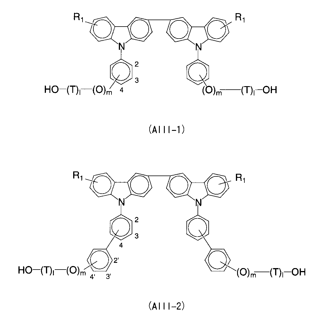
〔一般式(AI−1)および(AI−2)中、R1は水素原子、炭素数1〜8のアルキル基、アルコキシ基、または、置換もしくは未置換の芳香族基を表し、Tは炭素数1〜6の2価の直鎖状炭化水素、または、炭素数2〜10の分枝状炭化水素を表し、l、mは0または1を表す。〕 [In general formulas (AI-1) and (AI-2), R 1 represents a hydrogen atom, an alkyl group having 1 to 8 carbon atoms, an alkoxy group, or a substituted or unsubstituted aromatic group, and T represents carbon. A divalent linear hydrocarbon having 1 to 6 carbon atoms or a branched hydrocarbon having 2 to 10 carbon atoms is represented, and l and m represent 0 or 1. ]
<2> 前記有機化合物層が、少なくとも発光層と、電子輸送層および/または電子注入層とから構成され、
少なくとも前記発光層が、前記一般式(AI−1)および(AI−2)で示される構造から選択された少なくとも1種を部分構造として含む繰り返し単位よりなる電荷輸送性ポリエーテルを1種以上含有し、且つ、
前記発光層が、電子エネルギー準位の励起三重項状態から基底状態への遷移によりあるいは励起三重項状態を経由して基底状態への遷移により発光する発光性低分子を1種以上含有することを特徴とする<1>に記載の有機電界発光素子である。
<2> The organic compound layer is composed of at least a light emitting layer, an electron transport layer and / or an electron injection layer,
At least the light-emitting layer contains one or more charge transporting polyethers composed of repeating units containing at least one selected from the structures represented by the general formulas (AI-1) and (AI-2) as a partial structure And
The light emitting layer contains one or more luminescent small molecules that emit light by transition from an excited triplet state of an electron energy level to a ground state or by transition to a ground state via an excited triplet state. It is an organic electroluminescent element as described in <1> characterized.
<3> 前記発光層が、電荷輸送性材料を含むことを特徴とする<2>に記載の有機電界発光素子である。 <3> The organic electroluminescent element according to <2>, wherein the light emitting layer contains a charge transporting material.
<4> 前記有機化合物層が、少なくとも正孔輸送層および/または正孔注入層と、発光層と、電子輸送層および/または電子注入層とから構成され、
少なくとも前記発光層が、前記一般式(AI−1)および(AI−2)で示される構造から選択された少なくとも1種を部分構造として含む繰り返し単位よりなる電荷輸送性ポリエーテルを1種以上含有し、且つ、
前記発光層が、電子エネルギー準位の励起三重項状態から基底状態への遷移により、あるいは励起三重項状態を経由して基底状態への遷移により発光する発光性低分子を1種以上含有することを特徴とする<1>に記載の有機電界発光素子である。
<4> The organic compound layer is composed of at least a hole transport layer and / or a hole injection layer, a light emitting layer, an electron transport layer and / or an electron injection layer,
At least the light-emitting layer contains one or more charge transporting polyethers composed of repeating units containing at least one selected from the structures represented by the general formulas (AI-1) and (AI-2) as a partial structure And
The light-emitting layer contains one or more luminescent small molecules that emit light by transition from an excited triplet state to a ground state of an electron energy level or by transition from the excited triplet state to a ground state. The organic electroluminescent element according to <1>, wherein
<5> 前記発光層が、電荷輸送性材料を含むことを特徴とする<4>に記載の有機電界発光素子である。 <5> The organic electroluminescent element as described in <4>, wherein the light emitting layer contains a charge transporting material.
<6> 前記有機化合物層が、少なくとも正孔輸送層および/または正孔注入層と、発光層とから構成され、
少なくとも前記発光層が、前記一般式(AI−1)および(AI−2)で示される構造から選択された少なくとも1種を部分構造として含む繰り返し単位よりなる電荷輸送性ポリエーテルを1種以上含有し、且つ、
前記発光層が、電子エネルギー準位の励起三重項状態から基底状態への遷移により、あるいは励起三重項状態を経由して基底状態への遷移により発光する発光性低分子を1種以上含有することを特徴とする<1>に記載の有機電界発光素子である。
<6> The organic compound layer is composed of at least a hole transport layer and / or a hole injection layer, and a light emitting layer,
At least the light-emitting layer contains one or more charge transporting polyethers composed of repeating units containing at least one selected from the structures represented by the general formulas (AI-1) and (AI-2) as a partial structure And
The light-emitting layer contains one or more luminescent small molecules that emit light by transition from an excited triplet state to a ground state of an electron energy level or by transition from the excited triplet state to a ground state. The organic electroluminescent element according to <1>, wherein
<7> 前記発光層が、電荷輸送性材料を含むことを特徴とする<6>に記載の有機電界発光素子である。 <7> The organic electroluminescent element according to <6>, wherein the light emitting layer contains a charge transporting material.
<8> 前記有機化合物層が、少なくとも電荷輸送能を有する発光層から構成され、
前記発光層が、前記一般式(AI−1)および(AI−2)で示される構造から選択された少なくとも1種を部分構造として含む繰り返し単位よりなる電荷輸送性ポリエーテルを1種以上と、電子エネルギー準位の励起三重項状態から基底状態への遷移によりあるいは励起三重項状態を経由して基底状態への遷移により発光する発光性低分子とを含有することを特徴とする<1>に記載の有機電界発光素子である。
<8> The organic compound layer is composed of a light emitting layer having at least a charge transporting capability,
The light emitting layer includes at least one charge transporting polyether comprising a repeating unit containing at least one selected from the structures represented by the general formulas (AI-1) and (AI-2) as a partial structure; <1> characterized by containing a light-emitting small molecule that emits light by a transition from an excited triplet state to a ground state of an electron energy level or a transition to a ground state via an excited triplet state. It is an organic electroluminescent element of description.
<9> 前記発光層が、電荷輸送性材料を含むことを特徴とする<8>に記載の有機電界発光素子である。 <9> The organic electroluminescent element according to <8>, wherein the light emitting layer contains a charge transporting material.
<10> 前記一般式(AI−1)及び(AI−2)で示される構造から選択された少なくとも1種を部分構造として含む繰り返し単位よりなる電荷輸送性ポリエーテルが、下記一般式(AII)で示される電荷輸送性ポリエーテルであることを特徴とする<1>に記載の有機電界発光素子である。 <10> A charge transporting polyether comprising a repeating unit containing at least one selected from the structures represented by the general formulas (AI-1) and (AI-2) as a partial structure is represented by the following general formula (AII): <1> The organic electroluminescence device according to <1>, which is a charge transporting polyether represented by the formula:
(一般式(AII)中、Aは上記一般式(AI−1)及び(AI−2)で示される構造から選択された少なくとも1種を表し、Rは水素原子、アルキル基、置換もしくは未置換のアリール基、又は置換もしくは未置換のアラルキル基を表し、pは5〜5000の整数を表す。) (In the general formula (AII), A represents at least one selected from the structures represented by the general formulas (AI-1) and (AI-2), and R represents a hydrogen atom, an alkyl group, substituted or unsubstituted. Of the aryl group, or a substituted or unsubstituted aralkyl group, and p represents an integer of 5 to 5000.)
<11> 少なくとも一方が透明または半透明である一対の電極間に挾持された、1つまたは複数の有機化合物層より構成される有機電界発光素子において、前記有機化合物層の少なくとも1層が、下記一般式(BI−1)および(BI−2)で示される構造から選択された少なくとも1種を部分構造として含む繰り返し単位よりなる電荷輸送性ポリエーテルを1種以上と、電子エネルギー準位の励起三重項状態から基底状態への遷移によりあるいは励起三重項状態を経由して基底状態への遷移により発光する発光性低分子とを含有することを特徴とする有機電界発光素子である。 <11> In an organic electroluminescent element composed of one or more organic compound layers sandwiched between a pair of electrodes, at least one of which is transparent or translucent, at least one of the organic compound layers is: Excitation of electron energy level with at least one charge transporting polyether comprising a repeating unit containing at least one selected from structures represented by general formulas (BI-1) and (BI-2) as a partial structure An organic electroluminescence device comprising a light-emitting small molecule that emits light by transition from a triplet state to a ground state or by transition to a ground state via an excited triplet state.
〔一般式(BI−1)および(BI−2)中、R1は水素原子、炭素数1〜8のアルキル基、アルコキシ基、または、置換もしくは未置換の芳香族基を表し、Tは炭素数1〜6の2価の直鎖状炭化水素、または、炭素数2〜10の分枝状炭化水素を表し、l、mは0または1を表す。〕 [In General Formulas (BI-1) and (BI-2), R 1 represents a hydrogen atom, an alkyl group having 1 to 8 carbon atoms, an alkoxy group, or a substituted or unsubstituted aromatic group, and T represents carbon. A divalent linear hydrocarbon having 1 to 6 carbon atoms or a branched hydrocarbon having 2 to 10 carbon atoms is represented, and l and m represent 0 or 1. ]
<12> 前記有機化合物層が、少なくとも発光層と、電子輸送層および/または電子注入層とから構成され、
少なくとも前記発光層が、前記一般式(BI−1)および(BI−2)で示される構造から選択された少なくとも1種を部分構造として含む繰り返し単位よりなる電荷輸送性ポリエーテルを1種以上含有し、且つ、
前記発光層が、電子エネルギー準位の励起三重項状態から基底状態への遷移によりあるいは励起三重項状態を経由して基底状態への遷移により発光する発光性低分子を1種以上含有することを特徴とする<11>に記載の有機電界発光素子である。
<12> The organic compound layer is composed of at least a light emitting layer, an electron transport layer and / or an electron injection layer,
At least the light emitting layer contains one or more charge transporting polyethers composed of a repeating unit containing at least one selected from the structures represented by the general formulas (BI-1) and (BI-2) as a partial structure. And
The light emitting layer contains one or more luminescent small molecules that emit light by transition from an excited triplet state of an electron energy level to a ground state or by transition to a ground state via an excited triplet state. <11> characterized in that it is an organic electroluminescent element.
<13> 前記発光層が、電荷輸送性材料を含むことを特徴とする<12>に記載の有機電界発光素子である。 <13> The organic electroluminescent element according to <12>, wherein the light emitting layer contains a charge transporting material.
<14> 前記有機化合物層が、少なくとも正孔輸送層および/または正孔注入層と、発光層と、電子輸送層および/または電子注入層とから構成され、
少なくとも前記発光層が、前記一般式(BI−1)および(BI−2)で示される構造から選択された少なくとも1種を部分構造として含む繰り返し単位よりなる電荷輸送性ポリエーテルを1種以上含有し、且つ、
前記発光層が、電子エネルギー準位の励起三重項状態から基底状態への遷移によりあるいは励起三重項状態を経由して基底状態への遷移により発光する発光性低分子を1種以上含有することを特徴とする<11>に記載の有機電界発光素子である。
<14> The organic compound layer is composed of at least a hole transport layer and / or a hole injection layer, a light emitting layer, an electron transport layer and / or an electron injection layer,
At least the light emitting layer contains one or more charge transporting polyethers composed of a repeating unit containing at least one selected from the structures represented by the general formulas (BI-1) and (BI-2) as a partial structure. And
The light emitting layer contains one or more luminescent small molecules that emit light by transition from an excited triplet state of an electron energy level to a ground state or by transition to a ground state via an excited triplet state. <11> characterized in that it is an organic electroluminescent element.
<15> 前記発光層が、電荷輸送性材料を含むことを特徴とする<14>に記載の有機電界発光素子である。 <15> The organic electroluminescent element as described in <14>, wherein the light emitting layer contains a charge transporting material.
<16> 前記有機化合物層が、少なくとも正孔輸送層および/または正孔注入層と、発光層とから構成され、
少なくとも前記発光層が、前記一般式(BI−1)および(BI−2)で示される構造から選択された少なくとも1種を部分構造として含む繰り返し単位よりなる電荷輸送性ポリエーテルを1種以上含有し、且つ、
前記発光層が、電子エネルギー準位の励起三重項状態から基底状態への遷移により、あるいは励起三重項状態を経由して基底状態への遷移により発光する発光性低分子を1種以上含有することを特徴とする<11>に記載の有機電界発光素子である。
<16> The organic compound layer is composed of at least a hole transport layer and / or a hole injection layer, and a light emitting layer,
At least the light emitting layer contains one or more charge transporting polyethers composed of a repeating unit containing at least one selected from the structures represented by the general formulas (BI-1) and (BI-2) as a partial structure. And
The light-emitting layer contains one or more luminescent small molecules that emit light by transition from an excited triplet state to a ground state of an electron energy level or by transition from the excited triplet state to a ground state. <11> The organic electroluminescence device according to <11>.
<17> 前記発光層が、電荷輸送性材料を含むことを特徴とする<16>に記載の有機電界発光素子である。 <17> The organic electroluminescent element according to <16>, wherein the light emitting layer contains a charge transporting material.
<18> 前記有機化合物層が、少なくとも電荷輸送能を有する発光層から構成され、該発光層が、前記一般式(BI−1)および(BI−2)で示される構造から選択された少なくとも1種を部分構造として含む繰り返し単位よりなる電荷輸送性ポリエーテルを1種以上含有し、さらに、前記発光層が、電子エネルギー準位の励起三重項状態から基底状態への遷移によりあるいは励起三重項状態を経由して基底状態への遷移により発光する発光性低分子を含有することを特徴とする<11>に記載の有機電界発光素子である。 <18> The organic compound layer includes at least a light emitting layer having charge transporting ability, and the light emitting layer is at least one selected from the structures represented by the general formulas (BI-1) and (BI-2). Containing at least one charge transporting polyether comprising a repeating unit containing a species as a partial structure, and the light-emitting layer is formed by transition from an excited triplet state of an electron energy level to a ground state or an excited triplet state The organic electroluminescent device according to <11>, which contains a light-emitting small molecule that emits light by transition to a ground state via.
<19> 前記発光層が、電荷輸送性材料を含むことを特徴とする<18>に記載の有機電界発光素子である。 <19> The organic electroluminescent element as described in <18>, wherein the light emitting layer contains a charge transporting material.
<20> 前記一般式(BI−1)及び(BI−2)で示される構造から選択された少なくとも1種を部分構造として含む繰り返し単位よりなる電荷輸送性ポリエーテルが、下記一般式(BII)で示される電荷輸送性ポリエーテルであることを特徴とする<11>に記載の有機電界発光素子である。
(一般式(BII)中、Aは上記一般式(BI−1)及び(BI−2)で示される構造から選択された少なくとも1種を表し、Rは水素原子、アルキル基、置換もしくは未置換のアリール基、又は置換もしくは未置換のアラルキル基を表し、pは5〜5000の整数を表す。) (In the general formula (BII), A represents at least one selected from the structures represented by the general formulas (BI-1) and (BI-2), and R represents a hydrogen atom, an alkyl group, substituted or unsubstituted. Of the aryl group, or a substituted or unsubstituted aralkyl group, and p represents an integer of 5 to 5000.)
以上に説明したように本発明によれば、十分な輝度を有し、安定性及び耐久性に優れ、かつ大面積化可能であり製造容易な有機電界発光素子を提供することができる。 As described above, according to the present invention, it is possible to provide an organic electroluminescence device that has sufficient luminance, is excellent in stability and durability, can be increased in area, and can be easily manufactured.
本発明の有機EL素子は、少なくとも一方が透明または半透明である一対の電極間に挾持された、1つまたは複数の有機化合物層より構成される有機電界発光素子において、
前記有機化合物層の少なくとも1層が、下記一般式(AI−1)および(AI−2)、または、下記一般式(BI−1)および(BI−2)で示される構造から選択された少なくとも1種を部分構造として含む繰り返し単位よりなる電荷輸送性ポリエーテルを1種以上と、電子エネルギー準位の励起三重項状態から基底状態への遷移によりあるいは励起三重項状態を経由して基底状態への遷移により発光する発光性低分子(以下、「発光性低分子」と略す場合がある)とを含有することを特徴とする。
The organic EL device of the present invention is an organic electroluminescent device comprising one or more organic compound layers sandwiched between a pair of electrodes, at least one of which is transparent or translucent.
At least one of the organic compound layers is at least selected from the following general formulas (AI-1) and (AI-2) or structures represented by the following general formulas (BI-1) and (BI-2) One or more charge-transporting polyethers composed of repeating units containing one type as a partial structure, and transition to the ground state through the transition from the excited triplet state to the ground state of the electron energy level or via the excited triplet state It contains a light-emitting small molecule that emits light by the transition of (hereinafter sometimes abbreviated as “light-emitting low molecule”).
本発明の有機EL素子は、発光性低分子と、この発光性低分子のホスト材料としても機能する前記電荷輸送性ポリエーテルとを含有する層を有することで、十分な輝度を有し、安定性及び耐久性に優れる。さらに、前記電荷輸送性ポリエーテルを用いることで、大面積化可能であり、容易に製造可能である。
特に本発明では、前記電荷輸送性ポリエーテル及び前記発光性低分子を含有する層を湿式による塗布方式で形成することができるため、前述のような従来の素子に比べ、製造プロセスを大幅に簡易化することができる。
The organic EL device of the present invention has a layer containing a light-emitting low molecule and the charge transporting polyether that also functions as a host material of the light-emitting low molecule, so that it has sufficient luminance and is stable. Excellent in durability and durability. Further, by using the charge transporting polyether, the area can be increased and the production can be easily performed.
In particular, in the present invention, since the layer containing the charge transporting polyether and the light emitting low molecule can be formed by a wet coating method, the manufacturing process is greatly simplified compared to the conventional device as described above. Can be
なお、本発明では、下記一般式(AI−1)、一般式(AI−2)、一般式(BI−1)、あるいは、一般式(BI−2)で示されるようなカルバゾール構造を含む電荷輸送性ポリエーテルを用いるが、このようなカルバゾール構造を含む電荷輸送性ポリエーテルとしては、特開2005−259441号公報に記載のカルバゾール構造(いわゆる、4,4’−dicarbazoly−1,1’−biphenyl(CBP)類似の構造)を含む電荷輸送性ポリエーテルも挙げられる。
しかしながら、本発明で用いるカルバゾール構造を含む電荷輸送性ポリエーテルは、CBP構造を含む電荷輸送性ポリエーテルと比較して、溶媒に対する溶解性が優れていることから製膜が容易で形成された膜の均一性も良好である。また、混合する発光性低分子との相分離が生じにくい利点も有する。
In the present invention, a charge including a carbazole structure represented by the following general formula (AI-1), general formula (AI-2), general formula (BI-1), or general formula (BI-2) A transporting polyether is used. As the charge transporting polyether including such a carbazole structure, a carbazole structure described in JP-A-2005-259441 (so-called 4,4′-dicarbazoly-1,1′- Biphenyl (CBP) -like structure) is also included.
However, since the charge transporting polyether containing a carbazole structure used in the present invention is superior in solubility in a solvent as compared with the charge transporting polyether containing a CBP structure, the film can be formed easily. The uniformity is also good. In addition, there is an advantage that phase separation with the light emitting small molecule to be mixed hardly occurs.
次に、本発明の有機電界発光素子における、下記一般式(AI−1)および(AI−2)で示される構造から選択された少なくとも1種を部分構造として含む繰り返し単位よりなる電荷輸送性ポリエーテルについて説明する。 Next, in the organic electroluminescent device of the present invention, a charge transporting poly- mer comprising a repeating unit containing at least one selected from the structures represented by the following general formulas (AI-1) and (AI-2) as a partial structure. The ether will be described.
上記一般式(AI−1)および(AI−2)中、R1は炭素数1〜8のアルキル基、アルコキシ基、または、置換もしくは未置換の芳香族基を表す。
ここでいう芳香族基としては、フェニル基、トリル基、メトキシフェニル基のようなフェニル基誘導体、1−ナフチル基、2−ナフチル基、9−アントラニル基のような縮環系誘導体、チエニル基、メチルチエニル基、フラニル基、オキサジアゾール基のような複素環系誘導体が好適に用いられる。
また、Tは炭素数1〜6の2価の直鎖状炭化水素、または、炭素数2〜10の分枝状炭化水素を表し、l、mは0または1を表す。Tの具体的な構造としては、以下を挙げることができる。
In the general formulas (AI-1) and (AI-2), R 1 represents an alkyl group having 1 to 8 carbon atoms, an alkoxy group, or a substituted or unsubstituted aromatic group.
Examples of the aromatic group include phenyl group derivatives such as phenyl group, tolyl group and methoxyphenyl group, condensed ring derivatives such as 1-naphthyl group, 2-naphthyl group and 9-anthranyl group, thienyl group, Heterocyclic derivatives such as methylthienyl group, furanyl group and oxadiazole group are preferably used.
T represents a divalent linear hydrocarbon having 1 to 6 carbon atoms or a branched hydrocarbon having 2 to 10 carbon atoms, and l and m represent 0 or 1. Specific examples of T include the following.
一般式(AI−1)及び(AI−2)で示される構造から選択された少なくとも1種を部分構造として含む繰り返し単位よりなる電荷輸送性ポリエーテルとしては、下記一般式(AII)で示されるものが好適に使用される。 The charge transporting polyether comprising a repeating unit containing at least one selected from the structures represented by the general formulas (AI-1) and (AI-2) as a partial structure is represented by the following general formula (AII). Those are preferably used.
上記一般式(AII)式中、Aは上記一般式(AI−1)及び(AI−2)で示される構造から選択された少なくとも1種を表し、一つのポリマー中に2種類以上の構造Aが含まれていてもよい。 In the general formula (AII), A represents at least one selected from the structures represented by the general formulas (AI-1) and (AI-2), and two or more types of structures A are included in one polymer. May be included.
一般式(AII)式中、Rは水素原子、アルキル基、置換もしくは未置換のアリール基、又は置換もしくは未置換のアラルキル基を表す。アルキル基としては、炭素数1〜10のものが好ましく、例えば、メチル基、エチル基、プロピル基、イソプロピル基等が挙げられる。アリール基としては、炭素6〜20のものが好ましく、例えば、フェニル基、トルイル基等が挙げられる。アラルキル基としては、炭素数7〜20のものが好ましく、例えば、ベンジル基、フェネチル基等が挙げられる。また、置換アリール基、置換アラルキル基の置換基としては、水素原子、アルキル基、アルコキシ基、置換アミノ基、ハロゲン原子等が挙げられる。 In the general formula (AII), R represents a hydrogen atom, an alkyl group, a substituted or unsubstituted aryl group, or a substituted or unsubstituted aralkyl group. As an alkyl group, a C1-C10 thing is preferable, for example, a methyl group, an ethyl group, a propyl group, an isopropyl group etc. are mentioned. As the aryl group, those having 6 to 20 carbon atoms are preferable, and examples thereof include a phenyl group and a toluyl group. As the aralkyl group, those having 7 to 20 carbon atoms are preferable, and examples thereof include a benzyl group and a phenethyl group. In addition, examples of the substituent of the substituted aryl group and the substituted aralkyl group include a hydrogen atom, an alkyl group, an alkoxy group, a substituted amino group, and a halogen atom.
一般式(AII)式中、重合度を表わすpは5〜5000の範囲であるが、好ましくは10〜3000、より好ましくは15〜1000の範囲である。 In the general formula (AII), p representing the degree of polymerization is in the range of 5 to 5000, preferably 10 to 3000, and more preferably 15 to 1000.
電荷輸送性ポリエーテルの重合度pが、5未満であると、成膜性に劣り強固な膜が得られにくいという問題がある。また、電荷輸送性ポリエーテルの重合度pが5000より高いと、溶剤への溶解度が低くなり、加工性が悪くなる。 When the degree of polymerization p of the charge transporting polyether is less than 5, there is a problem that it is difficult to obtain a strong film due to inferior film formability. On the other hand, when the degree of polymerization p of the charge transporting polyether is higher than 5000, the solubility in a solvent is lowered and the processability is deteriorated.
また、本発明の電荷輸送性ポリエーテルの重量平均分子量Mwは5000〜1000000の範囲であるが、10000〜300000の範囲にあるのが好ましい。 The weight average molecular weight Mw of the charge transporting polyether of the present invention is in the range of 5,000 to 1,000,000, but is preferably in the range of 10,000 to 300,000.
本発明の、上記一般式(AI−1)及び(AI−2)で示される構造から選択された少なくとも1種を部分構造として含む繰り返し単位よりなる電荷輸送性ポリエーテルは、下記構造式(AIII−1)又は(AIII−2)で示される電荷輸送性モノマーを、例えば、第4版実験化学講座第28巻(丸善、1992)等に記載された公知の方法で重合させることによって合成することができる。なお、構造式(AIII−1)又は(AIII−2)中、R1、T、l、mは、前記一般式(AI−1)又は(AI−2)におけるR1、T、l、mと各々同様であるため詳細な説明を省略する。 The charge transporting polyether comprising a repeating unit containing at least one selected from the structures represented by the general formulas (AI-1) and (AI-2) as a partial structure of the present invention is represented by the following structural formula (AIII -1) or (AIII-2) is synthesized by polymerizing a charge transporting monomer represented by, for example, a known method described in the 4th edition, Experimental Chemistry Course Vol. 28 (Maruzen, 1992). Can do. Incidentally, in the structural formula (AIII-1) or (AIII-2), R 1 , T, l, m is, R 1 in the general formula (AI-1) or (AI-2), T, l, m Since these are the same as each other, detailed description is omitted.
上記一般式(AII)で示される電荷輸送性ポリエーテルは、次のようにして合成することができる。 The charge transporting polyether represented by the general formula (AII) can be synthesized as follows.
1)上記電荷輸送性ポリエーテルは、上記一般式(AIII−1)及び(AIII−2)のうち2個のヒドロキシアルキル基を有する電荷輸送性化合物(電荷輸送性モノマー)を加熱脱水縮合する方法によって合成することができる。この場合、無溶媒で電荷輸送性モノマーを加熱溶融し、水の脱離による重合反応を促進させるため減圧下で反応させることが望ましい。 1) The charge transporting polyether is a method of subjecting a charge transporting compound (charge transporting monomer) having two hydroxyalkyl groups in the general formulas (AIII-1) and (AIII-2) to heat dehydration condensation. Can be synthesized. In this case, it is desirable that the charge transporting monomer is heated and melted without a solvent and reacted under reduced pressure in order to promote a polymerization reaction due to elimination of water.
また、溶媒を使用する場合は、水の除去のため、水と共沸する溶媒、例えば、トリクロロエタン、トルエン、クロロベンゼン、ジクロロベンゼン、ニトロベンゼン、1−クロロナフタレン等が有効であり、電荷輸送性モノマー1当量に対して、1当量〜100当量、好ましくは2当量〜50当量の範囲で用いられる。反応温度は任意に設定できるが、重合中に生成する水を除去するために、溶媒の沸点で反応させるのが好ましい。重合が進まない場合には、反応系から溶媒を除去し、粘ちょう状態で加熱撹拌してもよい。
When a solvent is used, a solvent azeotroped with water, for example, trichloroethane, toluene, chlorobenzene, dichlorobenzene, nitrobenzene, 1-chloronaphthalene, etc. is effective for removing water, and the
2)上記電荷輸送性ポリエーテルは、酸触媒として、p−トルエンスルホン酸、塩酸、硫酸、トリフルオロ酢酸等のプロトン酸、あるいは塩化亜鉛等のルイス酸を用い脱水縮合する方法によって合成することもできる。この場合、電荷輸送性モノマー1当量に対して、酸触媒を1/10000当量〜1/10当量、好ましくは1/1000当量〜1/50当量の範囲で用いる。重合中に生成する水を除去するために、水と共沸可能な溶剤を用いるのが好ましい。 2) The above charge transporting polyether may be synthesized by a dehydration condensation method using a protonic acid such as p-toluenesulfonic acid, hydrochloric acid, sulfuric acid, trifluoroacetic acid or a Lewis acid such as zinc chloride as an acid catalyst. it can. In this case, the acid catalyst is used in the range of 1/10000 equivalent to 1/10 equivalent, preferably 1/1000 equivalent to 1/50 equivalent, per equivalent of charge transporting monomer. In order to remove water generated during the polymerization, it is preferable to use a solvent azeotropic with water.
溶剤としては、トルエン、クロロベンゼン、ジクロロベンゼン、ニトロベンゼン、1−クロロナフタレン等が有効であり、電荷輸送性モノマー1当量に対して、1当量〜100当量、好ましくは2当量〜50当量の範囲で用いられる。反応温度は任意に設定できるが、重合中に生成する水を除去するために、溶剤の沸点で反応させることが好ましい。 As the solvent, toluene, chlorobenzene, dichlorobenzene, nitrobenzene, 1-chloronaphthalene and the like are effective, and they are used in the range of 1 equivalent to 100 equivalents, preferably 2 equivalents to 50 equivalents with respect to 1 equivalent of the charge transporting monomer. It is done. The reaction temperature can be arbitrarily set, but it is preferable to carry out the reaction at the boiling point of the solvent in order to remove water generated during the polymerization.
3)上記電荷輸送性ポリエーテルは、イソシアン化シクロヘキシル等のイソシアン化アルキル、シアンン化シクロヘキシル等のイソシアン化アルキル、シアン酸p−トリルや2,2−ビス(4−シアナートフェニル)プロパン等のシアン酸エステル、ジクロロヘキシルカルボジイミド(DCC)、トリクロロアセトニトリル等の縮合剤を用いる方法によっても合成することができる。この場合、縮合剤は、電荷輸送性モノマー1当量に対して、1/2当量〜10当量、好ましくは1当量〜3当量の範囲で用いられる。 3) The above charge transporting polyethers include alkyl isocyanates such as cyclohexyl isocyanate, alkyl isocyanates such as cyclohexyl cyanide, and cyanides such as p-tolyl cyanate and 2,2-bis (4-cyanatophenyl) propane. It can also be synthesized by a method using a condensing agent such as acid ester, dichlorohexylcarbodiimide (DCC), or trichloroacetonitrile. In this case, the condensing agent is used in a range of 1/2 equivalent to 10 equivalents, preferably 1 equivalent to 3 equivalents, relative to 1 equivalent of the charge transporting monomer.
溶剤として、トルエン、クロロベンゼン、ジクロロベンゼン、1−クロロナフタレン等が有効であり、電荷輸送性モノマー1当量に対して、1当量〜100当量、好ましくは2〜50当量の範囲で用いられる。反応温度は任意に設定できるが、室温から溶剤の沸点で反応させることが好ましい。 As the solvent, toluene, chlorobenzene, dichlorobenzene, 1-chloronaphthalene and the like are effective, and 1 to 100 equivalents, preferably 2 to 50 equivalents, are used with respect to 1 equivalent of the charge transporting monomer. Although reaction temperature can be set arbitrarily, it is preferable to make it react from the room temperature to the boiling point of a solvent.
上記1)、2)及び3)の合成法のうち、異性化や副反応が起こりにくいことから、合成法1)又は3)が好ましい。特に、合成法3)が、反応条件がより穏和なことからより好ましい。 Of the synthesis methods 1), 2) and 3), the synthesis method 1) or 3) is preferred because isomerization and side reactions are unlikely to occur. In particular, the synthesis method 3) is more preferable because the reaction conditions are milder.
反応終了後、溶剤を用いなかった場合は溶解可能な溶剤に溶解させる。溶剤を用いた場合には、そのまま、メタノール、エタノール等のアルコール類や、アセトン等の電荷輸送性ポリマーが溶解しにくい貧溶剤中に滴下し、電荷輸送性ポリマーを析出させ、電荷輸送性ポリマーを分離した後、水や有機溶剤で十分に洗浄し、乾燥させる。 If the solvent is not used after completion of the reaction, it is dissolved in a soluble solvent. When a solvent is used, it is dropped as it is in a poor solvent in which alcohols such as methanol and ethanol and charge transporting polymers such as acetone are difficult to dissolve, to precipitate the charge transporting polymer, After separation, wash thoroughly with water or organic solvent and dry.
さらに必要であれば、適当な有機溶剤に溶解させ、貧溶剤中に滴下し、電荷輸送性ポリマーを析出させる再沈澱処理を繰り返してもよい。 Furthermore, if necessary, the reprecipitation treatment may be repeated in which it is dissolved in a suitable organic solvent and dropped into a poor solvent to precipitate the charge transporting polymer.
再沈澱処理の際には、メカニカルスターラー等で、効率よく撹拌しながら行うことが好ましい。再沈澱処理の際に電荷輸送性ポリマーを溶解させる溶剤は、電荷輸送性ポリマー1当量に対して、1当量〜100当量、好ましくは2当量〜50当量の範囲で用いられる。また、貧溶剤は電荷輸送性ポリマー1当量に対して、1当量〜1000当量、好ましくは10当量〜500当量の範囲で用いられる。さらに、上記反応において、電荷輸送性モノマーを2種以上、好ましくは2種〜5種、さらに好ましくは2種〜3種用いることにより、共重合ポリマーの合成も可能である。異種の電荷輸送性モノマーを共重合することによって、電気特性、成膜性、溶解性を制御することができる。 The reprecipitation treatment is preferably carried out with efficient stirring using a mechanical stirrer or the like. The solvent for dissolving the charge transporting polymer in the reprecipitation treatment is used in the range of 1 to 100 equivalents, preferably 2 to 50 equivalents, per 1 equivalent of the charge transporting polymer. The poor solvent is used in the range of 1 equivalent to 1000 equivalents, preferably 10 equivalents to 500 equivalents, relative to 1 equivalent of the charge transporting polymer. Furthermore, in the above reaction, a copolymer can be synthesized by using two or more charge transporting monomers, preferably 2 to 5 kinds, more preferably 2 to 3 kinds. By copolymerizing different kinds of charge transporting monomers, it is possible to control electrical characteristics, film formability, and solubility.
電荷輸送性ポリマーの末端基は、電荷輸送性モノマーと同様にヒドロキシル基、すなわちRが水素原子であってよいが、溶解性、成膜性、モビリティー等のポリマー物性に影響を及ぼす場合には、末端基Rを修飾し物性を制御することができる。例えば、末端のヒドロキシル基を、硫酸アルキル、ヨウ化アルキル等でアルキルエーテル化することができる。 The terminal group of the charge transporting polymer may be a hydroxyl group, that is, R may be a hydrogen atom, as in the case of the charge transporting monomer, but when the polymer physical properties such as solubility, film formability, and mobility are affected, The end group R can be modified to control the physical properties. For example, the terminal hydroxyl group can be alkyl etherified with alkyl sulfate, alkyl iodide or the like.
具体的な試薬としては、硫酸ジメチル、硫酸ジエチル、ヨウ化メチル、ヨウ化エチル等から任意に選ぶことができ、末端のヒドロキシル基1当量に対し1当量〜3当量、好ましくは1当量〜2当量の範囲で用いる。その際、塩基触媒を用いることができるが、塩基触媒として、水酸化ナトリウム、水酸化カリウム、水素化ナトリウム、ナトリウム金属等から任意に選ぶことができ、末端のヒドロキシル基1等量に対し1当量〜3当量、好ましくは1当量〜2当量の範囲で用いる。 The specific reagent can be arbitrarily selected from dimethyl sulfate, diethyl sulfate, methyl iodide, ethyl iodide, etc., and 1 equivalent to 3 equivalents, preferably 1 equivalent to 2 equivalents, per 1 equivalent of the terminal hydroxyl group. Use within the range. In this case, a base catalyst can be used, but the base catalyst can be arbitrarily selected from sodium hydroxide, potassium hydroxide, sodium hydride, sodium metal, etc., and 1 equivalent with respect to 1 equivalent of the terminal hydroxyl group. -3 equivalents, preferably 1 equivalent to 2 equivalents.
反応温度は、0℃から使用する溶剤の沸点で行うことができる。また、その際用いる溶剤として、ベンゼン、トルエン、塩化メチレン、テトラヒドロフラン、N,N-ジメチルホルムアミド、ジメチルスルホキシド、N−メチルピロリドン、1,3−ジメチル−2−イミダゾリジノン等の不活性溶剤から選んだ単独溶剤、あるいは2〜3種の混合溶剤が使用できる。 The reaction temperature can be from 0 ° C. to the boiling point of the solvent used. In addition, the solvent used at that time is selected from inert solvents such as benzene, toluene, methylene chloride, tetrahydrofuran, N, N-dimethylformamide, dimethyl sulfoxide, N-methylpyrrolidone, and 1,3-dimethyl-2-imidazolidinone. However, a single solvent or a mixed solvent of 2 to 3 types can be used.
また、反応によっては、相間移動触媒としてテトラ−n−ブチルアンモニウムアイオダイド等の第4級アンモニウム塩を使用することもできる。また、末端のヒドロキシル基を、酸ハロゲン化物を用いアシル化して、基Rをアシル基にすることもできる。酸ハロゲン化物は特に限定するものではないが、例えばアクリロイルクロリド、クロトノイルクロリド、メタクリロイルクロリド、n−ブチルクロリド、2−フロイルクロリド、ベンゾイルクロリド、シクロヘキサンカルボニルクロリド、エナンチルクロリド、フェニルアセチルクロリド、o-トルオイルクロリド、m-トルオイルクロリド、p−トルオイルクロリド等があげられ、末端のヒドロキシル基1当量に対し1当量〜3当量、好ましくは1当量〜2当量の範囲で用いる。その際、塩基触媒を用いることができるが、塩基触媒としては、ピリジン、ジメチルアミノピリジン、トリメチルアミン、トリエチルアミン等から任意に選ぶことができ、酸クロリドに対し1当量〜3当量、好ましくは1当量〜2当量の範囲で用いる。その際用いる溶剤として、ベンゼン、トルエン、塩化メチルン、テトラヒドロフラン、メチルエチルケトン等があげられる。 Depending on the reaction, a quaternary ammonium salt such as tetra-n-butylammonium iodide can be used as a phase transfer catalyst. It is also possible to acylate the terminal hydroxyl group using an acid halide to convert the group R into an acyl group. The acid halide is not particularly limited. For example, acryloyl chloride, crotonoyl chloride, methacryloyl chloride, n-butyl chloride, 2-furoyl chloride, benzoyl chloride, cyclohexanecarbonyl chloride, enanthyl chloride, phenylacetyl chloride, o -Toluoyl chloride, m-toluoyl chloride, p-toluoyl chloride, etc. are mentioned, and it is used in the range of 1 to 3 equivalents, preferably 1 to 2 equivalents with respect to 1 equivalent of the terminal hydroxyl group. In this case, a base catalyst can be used, and the base catalyst can be arbitrarily selected from pyridine, dimethylaminopyridine, trimethylamine, triethylamine and the like, and is 1 to 3 equivalents, preferably 1 to 3 equivalents with respect to the acid chloride. Used in the range of 2 equivalents. Examples of the solvent used at that time include benzene, toluene, methyl chloride, tetrahydrofuran, and methyl ethyl ketone.
反応は、0℃から溶剤の沸点で行うことができる。好ましくは、0℃から30℃の範囲で行う。さらに、無水酢酸等の酸無水物を用いてもアシル化することができる。溶剤を用いる場合は、具体的には、ベンゼン、トルエン、クロロベンゼン等の不活性溶剤を使用することができる。反応は、0℃から溶剤の沸点で行うことができる。好ましくは、50℃から溶剤の沸点で行えばよい。 The reaction can be carried out from 0 ° C. to the boiling point of the solvent. Preferably, it is performed in the range of 0 ° C to 30 ° C. Furthermore, acylation can also be performed using an acid anhydride such as acetic anhydride. When using a solvent, specifically, an inert solvent such as benzene, toluene or chlorobenzene can be used. The reaction can be carried out from 0 ° C. to the boiling point of the solvent. Preferably, it may be carried out from 50 ° C. to the boiling point of the solvent.
そのほか、モノイソシアネートを用い、末端にウレタン残基(―CONH―R’)を導入することができる。具体的なモノイソシアネートとしては、イソシアン酸ベンジルエステル、イソシアン酸n−ブチルエステル、イソシアン酸t−ブチルエステル、イソシアン酸シクロヘキシルエステル、イソシアン酸2,6−ジメチルエステル、イソシアン酸エチルエステル、イソシアン酸イソプロピルエステル、イソシアン酸2−メトキシフェニルエステル、イソシアン酸4−メトキシフェニルエステル、イソシアン酸n−オクタデシルエステル、イソシアン酸フェニルエステル、イソシアン酸i−プロピルエステル、イソシアン酸m−トリルエステル、イソシアン酸p−トリルエステル、イソシアン酸1−ナフチルエステル等から任意に選ぶことができ、末端のヒドロキシル基1当量に対し1当量〜3当量、好ましくは1当量〜2当量の範囲で用いる。
In addition, a urethane residue (—CONH—R ′) can be introduced at the terminal using monoisocyanate. Specific monoisocyanates include isocyanic acid benzyl ester, isocyanic acid n-butyl ester, isocyanic acid t-butyl ester, isocyanic acid cyclohexyl ester,
その際用いる溶剤として、ベンゼン、トルエン、クロロベンゼン、ジクロロベンゼン、塩化メチレン、テトラヒドロフラン、N,N−ジメチルホルムアミド、ジメチルスルホキシド、N−メチルピロリドン、1,3−ジメチル−2−イミダゾリジノン等をあげることができる。 Examples of solvents used in this case include benzene, toluene, chlorobenzene, dichlorobenzene, methylene chloride, tetrahydrofuran, N, N-dimethylformamide, dimethyl sulfoxide, N-methylpyrrolidone, 1,3-dimethyl-2-imidazolidinone and the like. Can do.
反応温度は、0℃から使用溶剤の沸点で行うことができる。反応が進みにくい場合は、ジラウリン酸ジブチルスズ(II)、オクチル酸スズ(II)、ナフテン酸鉛等の金属化合物、あるいはトリエチルアミン、トリメチルアミン、ピリジン、ジメチルアミノピリジン等の3級アミンを触媒として添加することもできる。 The reaction temperature can be from 0 ° C. to the boiling point of the solvent used. If the reaction is difficult to proceed, add a metal compound such as dibutyltin (II) dilaurate, tin (II) octylate, lead naphthenate, or tertiary amines such as triethylamine, trimethylamine, pyridine, dimethylaminopyridine as a catalyst. You can also.
次に、本発明の有機電界発光素子における、下記一般式(BI−1)および(BI−2)で示される構造から選択された少なくとも1種を部分構造として含む繰り返し単位よりなる電荷輸送性ポリエーテルについて説明する。 Next, in the organic electroluminescent element of the present invention, a charge transporting poly- mer comprising a repeating unit containing at least one selected from the structures represented by the following general formulas (BI-1) and (BI-2) as a partial structure. The ether will be described.
上記一般式(BI−1)および(BI−2)中、R1は炭素数1〜8のアルキル基、アルコキシ基、または、置換もしくは未置換の芳香族基を表す。
ここでいう芳香族基としては、フェニル基、トリル基、メトキシフェニル基のようなフェニル基誘導体、1−ナフチル基、2−ナフチル基、9−アントラニル基のような縮環系誘導体、チエニル基、メチルチエニル基、フラニル基、オキサジアゾール基のような複素環系誘導体が好適に用いられる。
また、Tは炭素数1〜6の2価の直鎖状炭化水素、または、炭素数2〜10の分枝状炭化水素を表し、l、mは0または1を表す。Tの具体的な構造としては、以下を挙げることができる。
In the general formulas (BI-1) and (BI-2), R 1 represents an alkyl group having 1 to 8 carbon atoms, an alkoxy group, or a substituted or unsubstituted aromatic group.
Examples of the aromatic group include phenyl group derivatives such as phenyl group, tolyl group and methoxyphenyl group, condensed ring derivatives such as 1-naphthyl group, 2-naphthyl group and 9-anthranyl group, thienyl group, Heterocyclic derivatives such as methylthienyl group, furanyl group and oxadiazole group are preferably used.
T represents a divalent linear hydrocarbon having 1 to 6 carbon atoms or a branched hydrocarbon having 2 to 10 carbon atoms, and l and m represent 0 or 1. Specific examples of T include the following.
上記一般式(BI−1)及び(BI−2)で示される構造から選択された少なくとも1種を部分構造として含む繰り返し単位よりなるホール輸送性ポリエーテル(電荷輸送性ポリエーテル)としては、下記一般式(BII)で示されるものが好適に使用される。 As a hole transporting polyether (charge transporting polyether) comprising a repeating unit containing at least one selected from the structures represented by the general formulas (BI-1) and (BI-2) as a partial structure, Those represented by the general formula (BII) are preferably used.
上記一般式(BII)中、Aは前記一般式(BI−1)及び(BI−2)で示される構造から選択された少なくとも1種を表し、一つのポリマー中に2種類以上の構造のAが含まれてもよい。 In the general formula (BII), A represents at least one selected from the structures represented by the general formulas (BI-1) and (BI-2), and one polymer has two or more types of A. May be included.
また、一般式(BII)中、Rは水素原子、アルキル基、置換もしくは未置換のアリール基、又は置換もしくは未置換のアラルキル基を表す。上記アルキル基としては、炭素数が1〜10のものが好ましく、例えば、メチル基、エチル基、プロピル基、イソプロピル基、ブチル基、オクチル基、2-エチル−ヘキシル基等が挙げられる。前記アリール基としては、炭素数が6〜20のものが好ましく、例えば、フェニル基、トルイル基等が挙げられる。前記アラルキル基としては、炭素数が7〜20のものが好ましく、例えば、ベンジル基、フェネチル基等が挙げられる。また、前記置換アリール基、置換アラルキル基の置換基としては、水素原子、アルキル基、アルコキシ基、置換アミノ基、ハロゲン原子等が挙げられる。 In general formula (BII), R represents a hydrogen atom, an alkyl group, a substituted or unsubstituted aryl group, or a substituted or unsubstituted aralkyl group. As said alkyl group, a C1-C10 thing is preferable, For example, a methyl group, an ethyl group, a propyl group, an isopropyl group, a butyl group, an octyl group, 2-ethyl-hexyl group etc. are mentioned. As said aryl group, a C6-C20 thing is preferable, For example, a phenyl group, a toluyl group, etc. are mentioned. As said aralkyl group, a C7-C20 thing is preferable, For example, a benzyl group, a phenethyl group, etc. are mentioned. Examples of the substituent for the substituted aryl group and the substituted aralkyl group include a hydrogen atom, an alkyl group, an alkoxy group, a substituted amino group, and a halogen atom.
一般式(BII)中、電荷輸送性ポリマーの重合度を表すpは、5〜5000の範囲に設定され、好ましくは、10〜3000、より好ましくは15〜1000の範囲に設定される。
電荷輸送性ポリエーテルの重合度pが、5未満であると、成膜性に劣り強固な膜が得られにくいという問題がある。また、電荷輸送性ポリエーテルの重合度pが5000より高いと、溶剤への溶解度が低くなり、加工性が悪くなる。
In general formula (BII), p representing the degree of polymerization of the charge transporting polymer is set in the range of 5 to 5000, preferably 10 to 3000, and more preferably 15 to 1000.
When the degree of polymerization p of the charge transporting polyether is less than 5, there is a problem that it is difficult to obtain a strong film due to inferior film formability. On the other hand, when the degree of polymerization p of the charge transporting polyether is higher than 5000, the solubility in a solvent is lowered and the processability is deteriorated.
また、本発明の電荷輸送性ポリエーテルの重量平均分子量Mwは5000〜1000000の範囲であるが、10000〜300000の範囲にあるのが好ましい。 The weight average molecular weight Mw of the charge transporting polyether of the present invention is in the range of 5,000 to 1,000,000, but is preferably in the range of 10,000 to 300,000.
一般式(BI−1)又は一般式(BI−2)に示される構造から選択された少なくとも一種を部分構造として含む繰返し単位よりなる電荷輸送性ポリエーテルは、下記構造式(BIII−1)又は(BIII−2)で示される電荷輸送性モノマーを、例えば、第4版実験化学講座第28巻(丸善、1993)等に記載された公知の方法で重合させることによって合成することができる。なお、下記構造式(BIII−1)又は(BIII−2)中、T、l、mは、前記一般式(BI−1)及び一般式(BI−2)におけるT、l、mと各々同様である。また、下記構造式(BIII−1)又は(BIII−2)中、R1、R2は、前記一般式(BI−1)及び一般式(BI−2)におけるR1と同様である。
The charge transporting polyether comprising a repeating unit containing at least one selected from the structure represented by the general formula (BI-1) or the general formula (BI-2) as a partial structure is represented by the following structural formula (BIII-1) or The charge transporting monomer represented by (BIII-2) can be synthesized by polymerizing by a known method described in, for example, the 4th edition Experimental Chemistry Course Vol. 28 (Maruzen, 1993). In the following structural formula (BIII-1) or (BIII-2), T, l, and m are the same as T, l, and m in the general formula (BI-1) and general formula (BI-2), respectively. It is. Further, in the following structural formula (BIII-1) or (BIII-2), R 1 ,
上記一般式(BII)で示される電荷輸送性ポリエーテルは、次のようにして合成することができる。 The charge transporting polyether represented by the general formula (BII) can be synthesized as follows.
1)上記電荷輸送性ポリエーテルは、上記2個のヒドロキシアルキル基を有する電荷輸送性化合物(電荷輸送性モノマー)を加熱脱水縮合する方法によって合成することができる。この場合、無溶剤で電荷輸送性モノマーを加熱溶融し、水の脱水による重合反応促進させるために減圧下で反応させることが望ましい。また、溶媒を使用する場合は、水の除去のため、水と共沸する溶媒、例えばトリクロロエタン、トルエン、クロロベンゼン、ジクロロベンゼン、ニトロベンゼン、1−クロロナフタレン等が有効であり、電荷輸送性モノマー1当量に対して、1当量〜100当量、好ましくは2当量〜50当量の範囲で用いられる。反応温度は任意に設定できるが、重合中に生成する水を除去するために、溶媒の沸点で反応させるのが好ましい。重合が進まない場合には、反応系から溶媒を除去し、粘ちょう状態で加熱攪拌してもよい。
1) The charge transporting polyether can be synthesized by a method in which the charge transporting compound (charge transporting monomer) having the two hydroxyalkyl groups is subjected to heat dehydration condensation. In this case, it is desirable to heat and melt the charge transporting monomer without solvent and to react under reduced pressure in order to promote the polymerization reaction by dehydration of water. In the case of using a solvent, a solvent azeotropic with water, for example, trichloroethane, toluene, chlorobenzene, dichlorobenzene, nitrobenzene, 1-chloronaphthalene, etc. is effective for removing water, and 1 equivalent of a
2)上記電荷輸送性ポリエーテルは、酸触媒として、p−トルエンスルホン酸、塩酸、硫酸、トリフルオロ酢酸等のプロトン酸、或いは、塩化亜鉛等のルイス酸を用い脱水縮合する方法によって合成することもできる。この場合、電荷輸送性モノマー1当量に対して、酸触媒を1/10000当量〜1/10当量、好ましくは1/1000当量〜1/50当量の範囲で用いる。重合中に生成する水を除去するために、水と共沸可能な溶剤を用いるのが好ましい。溶媒としては、トルエン、クロロベンゼン、ジクロロベンゼン、ニトロベンゼン、1−クロロナフタレン等が有効であり、電荷輸送性モノマー1当量に対して、1当量〜100当量、好ましくは2当量〜50当量の範囲で用いられる。反応温度は任意に設定できるが、重合中に生成する水を除去するために、溶媒の沸点で反応させるのが好ましい。 2) The charge transporting polyether is synthesized by a dehydration condensation method using a protonic acid such as p-toluenesulfonic acid, hydrochloric acid, sulfuric acid, trifluoroacetic acid or a Lewis acid such as zinc chloride as an acid catalyst. You can also. In this case, the acid catalyst is used in the range of 1/10000 equivalent to 1/10 equivalent, preferably 1/1000 equivalent to 1/50 equivalent, per equivalent of the charge transporting monomer. In order to remove water generated during the polymerization, it is preferable to use a solvent azeotropic with water. As the solvent, toluene, chlorobenzene, dichlorobenzene, nitrobenzene, 1-chloronaphthalene and the like are effective, and they are used in a range of 1 equivalent to 100 equivalents, preferably 2 equivalents to 50 equivalents with respect to 1 equivalent of the charge transporting monomer. It is done. The reaction temperature can be arbitrarily set, but it is preferable to carry out the reaction at the boiling point of the solvent in order to remove water generated during the polymerization.
3)上記電荷輸送性ポリエーテルは、イソシアン化シクロヘキシル等のイソシアン化アルキル、シアン酸p−トリルや2,2−ビス(4−シアナートフェニル)プロパン等のシアン酸エステル、ジクロロヘキシルカルボジイミド(DCC)、トリクロロアセトニトリル等の縮合剤を用いる方法によっても合成することができる。この場合、縮合剤は、電荷輸送性モノマー1当量に対して、1/2当量〜10当量、好ましくは、1当量〜3当量の範囲で用いられる。溶媒として、トルエン、クロロベンゼン、ジクロロベンゼン、1−クロロナフタレン等が有効であり、電荷輸送性モノマー1当量に対して、1当量〜100当量、好ましくは2当量〜50当量の範囲で用いられる。反応温度は任意に設定できるが、室温から溶剤の沸点で反応させるのが好ましい。 3) The above charge transporting polyethers are alkyl isocyanates such as cyclohexyl isocyanate, cyanate esters such as p-tolyl cyanate and 2,2-bis (4-cyanatophenyl) propane, and dichlorocarbodiimide (DCC). It can also be synthesized by a method using a condensing agent such as trichloroacetonitrile. In this case, the condensing agent is used in a range of 1/2 equivalent to 10 equivalents, preferably 1 equivalent to 3 equivalents, relative to 1 equivalent of the charge transporting monomer. As the solvent, toluene, chlorobenzene, dichlorobenzene, 1-chloronaphthalene and the like are effective, and they are used in the range of 1 equivalent to 100 equivalents, preferably 2 equivalents to 50 equivalents, relative to 1 equivalent of the charge transporting monomer. Although reaction temperature can be set arbitrarily, it is preferable to make it react by the boiling point of a solvent from room temperature.
上記1)、2)、及び3)の合成法のうち、異性化や副反応が起こりにくいことから、合成法1)又は3)が好ましい。特に合成法3)は反応条件が穏和なことからより好ましい。 Of the synthesis methods 1), 2), and 3), the synthesis method 1) or 3) is preferable because isomerization and side reactions hardly occur. In particular, the synthesis method 3) is more preferable because the reaction conditions are mild.
反応終了後、溶剤を用いなかった場合は溶解可能な溶剤に溶解させる。溶剤を用いた場合には、そのまま、メタノール、エタノール等のアルコール類や、アセトン等の電荷輸送性ポリマーが溶解しにくい貧溶剤中に滴下し、電荷輸送性ポリマーを析出させ、電荷輸送性ポリマーを分離した後、水や有機溶剤で十分に洗浄し、乾燥させる。さらに必要であれば、適当な有機溶剤に溶解させ、貧溶剤中に滴下し、電荷輸送性ポリマーを析出させる再沈澱処理を繰り返してもよい。 If the solvent is not used after completion of the reaction, it is dissolved in a soluble solvent. When a solvent is used, it is dropped as it is in a poor solvent in which alcohols such as methanol and ethanol and charge transporting polymers such as acetone are difficult to dissolve, to precipitate the charge transporting polymer, After separation, wash thoroughly with water or organic solvent and dry. Furthermore, if necessary, the reprecipitation treatment may be repeated in which it is dissolved in a suitable organic solvent and dropped into a poor solvent to precipitate the charge transporting polymer.
再沈澱処理の際には、メカニカルスターラー等で効率よく攪拌しながら行うことが好ましい。再沈殿処理の際に、電荷輸送性ポリマーを溶解させる溶剤は、電荷輸送性ポリマー1当量に対して、1当量〜100当量、好ましくは2当量〜50当量の範囲で用いられる。また、貧溶剤は電荷輸送性ポリマー1当量に対して、1当量〜1000当量、好ましくは10当量〜500当量の範囲で用いられる。さらに上記反応において、電荷輸送性モノマーを2種以上、好ましくは2種〜5種、さらに好ましくは2種〜3種用いることにより、共重合ポリマーの合成も可能である。異種の電荷輸送性モノマーを共重合することによって、電気特性、成膜性、溶解性を制御することができる。 The reprecipitation treatment is preferably performed while stirring efficiently with a mechanical stirrer or the like. In the reprecipitation treatment, the solvent for dissolving the charge transporting polymer is used in the range of 1 equivalent to 100 equivalents, preferably 2 equivalents to 50 equivalents, relative to 1 equivalent of the charge transporting polymer. The poor solvent is used in the range of 1 equivalent to 1000 equivalents, preferably 10 equivalents to 500 equivalents, relative to 1 equivalent of the charge transporting polymer. Furthermore, in the above reaction, a copolymer can be synthesized by using two or more charge transporting monomers, preferably 2 to 5 types, more preferably 2 to 3 types. By copolymerizing different kinds of charge transporting monomers, it is possible to control electrical characteristics, film formability, and solubility.
電荷輸送性ポリマーの末端基は、電荷輸送性モノマーと同様に、ヒドロキシル基、すなわちRが水素原子であってよいが、溶解性、成膜性、モビリティー等のポリマー物性に影響を及ぼす場合には、末端基Rを修飾し物性を制御することができる。 The terminal group of the charge transporting polymer may be a hydroxyl group, that is, R may be a hydrogen atom, as in the case of the charge transporting monomer, but in the case of affecting the polymer physical properties such as solubility, film formability, and mobility. The end group R can be modified to control the physical properties.
例えば、末端のヒドロキシル基を、硫酸アルキル、ヨウ化アルキル等でアルキルエーテル化することができる。具体的な試薬としては、硫酸ジメチル、硫酸ジエチル、ヨウ化メチル、ヨウ化エチル等から任意に選ぶことができ、末端のヒドロキシル基に対して、1当量〜3当量、好ましくは、1当量〜2当量の範囲で用いる。その際、塩基触媒を用いることができるが、塩基触媒として、水酸化ナトリウム、水酸化カリウム、水素化ナトリウム、ナトリウム金属等から任意に選ぶことができ、末端のヒドロキシル基に対し、0.9当量〜3当量、好ましくは、1当量〜2当量の範囲で用いられる。 For example, the terminal hydroxyl group can be alkyl etherified with alkyl sulfate, alkyl iodide or the like. The specific reagent can be arbitrarily selected from dimethyl sulfate, diethyl sulfate, methyl iodide, ethyl iodide and the like, and is 1 equivalent to 3 equivalents, preferably 1 equivalent to 2 equivalents with respect to the terminal hydroxyl group. Use within an equivalent range. In this case, a base catalyst can be used, but the base catalyst can be arbitrarily selected from sodium hydroxide, potassium hydroxide, sodium hydride, sodium metal, etc., and 0.9 equivalent to the terminal hydroxyl group. -3 equivalents, preferably 1 equivalent to 2 equivalents.
反応温度は、0℃から使用する溶剤の沸点で行うことができる。また、その際用いる溶剤として、ベンゼン、トルエン、塩化メチレン、テトラヒドロフラン、N,N−ジメチルホルムアミド、ジメチルスルホキシド、N−メチルピロリドン、1,3−ジメチル−2−イミダゾリジノン等の不活性溶剤から選んだ単独溶剤、あるいは2種〜3種の混合溶剤が使用できる。
また、反応によっては、相間移動触媒としてテトラ−n−ブチルアンモニウムアイオダイド等の第4級アンモニウム塩を使用することもできる。また、末端のヒドロキシル基を、酸ハロゲン化物を用いてアシル化し、基Rをアシル基にすることもできる
The reaction temperature can be from 0 ° C. to the boiling point of the solvent used. In addition, the solvent used at that time is selected from inert solvents such as benzene, toluene, methylene chloride, tetrahydrofuran, N, N-dimethylformamide, dimethyl sulfoxide, N-methylpyrrolidone, 1,3-dimethyl-2-imidazolidinone. However, a single solvent or a mixed solvent of 2 to 3 types can be used.
Depending on the reaction, a quaternary ammonium salt such as tetra-n-butylammonium iodide may be used as a phase transfer catalyst. It is also possible to acylate the terminal hydroxyl group with an acid halide to make the group R an acyl group.
酸ハロゲン化物は特に限定するものではないが、例えば、アクリロイルクロリド、クロトノイルクロリド、メタクリロイルクロリド、n−ブチルクロリド、2−フロイルクロリド、ベンゾイルクロリド、シクロヘキサンカルボニルクロライド、エナンチルクロリド、フェニルアセチルクロリド、o−トルオイルクロリド、m−トルオイルクロリド、p−トルオイルクロリド等が挙げられ、末端のヒドロキシル基に対して、1当量〜3当量、好ましくは、1当量〜2当量の範囲で用いる。 Although the acid halide is not particularly limited, for example, acryloyl chloride, crotonoyl chloride, methacryloyl chloride, n-butyl chloride, 2-furoyl chloride, benzoyl chloride, cyclohexanecarbonyl chloride, enanthyl chloride, phenylacetyl chloride, o-Toluoyl chloride, m-toluoyl chloride, p-toluoyl chloride and the like can be mentioned, and it is used in the range of 1 to 3 equivalents, preferably 1 to 2 equivalents with respect to the terminal hydroxyl group.
その際、塩基触媒を用いることができるが、塩基触媒をしては、ピリジン、ジメチルアミノピリジン、トリメチルアミン、トリエチルアミン等から任意に選ぶことができ、酸クロリドに対し1当量〜3当量、好ましくは1当量〜2当量の範囲で用いる。その際用いる溶剤として、ベンゼン、トルエン、塩化メチレン、テトラヒドロフラン、メチルエチルケトン等が挙げられる。反応は、0℃から使用する溶剤の沸点で行うことができる。好ましくは、0℃から30℃の範囲で用いる。 In this case, a base catalyst can be used, and the base catalyst can be arbitrarily selected from pyridine, dimethylaminopyridine, trimethylamine, triethylamine, and the like, and is 1 to 3 equivalents, preferably 1 to the acid chloride. Used in the range of equivalent to 2 equivalents. Examples of the solvent used at that time include benzene, toluene, methylene chloride, tetrahydrofuran, and methyl ethyl ketone. The reaction can be carried out from 0 ° C. at the boiling point of the solvent used. Preferably, it is used in the range of 0 ° C to 30 ° C.
さらに、無水酢酸等の酸無水物を用いてもアシル化することができる。溶剤を用いる場合は、具体的には、ベンゼン、トルエン、クロロベンゼン等の不活性溶剤を使用することができる。反応は、0℃から溶剤の沸点で行うことができる。好ましくは、50℃から溶剤の沸点で行えばよい。そのほか、モノイソシアネートを用い、末端にウレタン残基(−CONH−R’)を導入することができる。具体的なモノイソシアネートとしてはイソシアン酸ベンジルエステル、イソシアン酸n−ブチルエステル、イソシアン酸t−ブチルエステル、イソシアン酸シクロヘキシルエステル、イソシアン酸2,6−ジメチルエステル、イソシアン酸エチルエステル、イソシアン酸イソプロピルエステル、イソシアン酸2−メトキシフェニルエステル、イソシアン酸4−メトキシフェニルエステル、イソシアン酸n−オクタデシルエステル、イソシアン酸フェニルエステル、イソシアン酸イソプロピルエステル、イソシアン酸m−トリルエステル、イソシアン酸p−トリルエステル、イソシアン酸1−ナフチルエステル等から任意に選ぶことができ、末端のヒドロキシル基に対し、1当量〜3当量、好ましくは1当量〜2当量の範囲で用いる。その際用いる溶剤として、ベンゼン、トルエン、クロロベンゼン、ジクロロベンゼン、塩化メチレン、テトラヒドロフラン、N,N−ジメチルホルムアミド、ジメチルスルホキシド、N−メチルピロリドン、1,3−ジメチル−2−イミダゾリジノン等を挙げることができる。
Furthermore, acylation can also be performed using an acid anhydride such as acetic anhydride. When using a solvent, specifically, an inert solvent such as benzene, toluene or chlorobenzene can be used. The reaction can be carried out from 0 ° C. to the boiling point of the solvent. Preferably, it may be carried out from 50 ° C. to the boiling point of the solvent. In addition, a urethane residue (—CONH—R ′) can be introduced at the terminal using monoisocyanate. Specific monoisocyanates include isocyanic acid benzyl ester, isocyanic acid n-butyl ester, isocyanic acid t-butyl ester, isocyanic acid cyclohexyl ester,
反応温度は、0℃から使用溶剤の沸点で行うことができる。反応が進みにくい場合は、ジラウリン酸ジブチルスズ(II)、オクチルスズ(II)、ナフテン酸鉛等の金属化合物、あるいは、トリエチルアミン、トリメチルアミン、ピリジン、ジメチルアミノピリジン等の3級アミンを触媒として添加することもできる。 The reaction temperature can be from 0 ° C. to the boiling point of the solvent used. If the reaction is difficult to proceed, a metal compound such as dibutyltin (II) dilaurate, octyltin (II), lead naphthenate, or a tertiary amine such as triethylamine, trimethylamine, pyridine, dimethylaminopyridine may be added as a catalyst. it can.
次に、発光性低分子について説明する。
本発明に用いられる発光性低分子には、固体状態で電子エネルギー準位の励起三重項状態から基底状態への遷移あるいは励起三重項状態を経由して基底状態への遷移により発光を示す化合物が用いられる。なお、本発明において「発光性低分子」とは、高分子のような重合により連結された繰り返し構造を持たない発光性の分子を意味する。
Next, the luminescent small molecule will be described.
The light-emitting small molecule used in the present invention includes a compound that emits light by transition from an excited triplet state of an electronic energy level to a ground state in a solid state or from a ground state via an excited triplet state. Used. In the present invention, the “light-emitting small molecule” means a light-emitting molecule that does not have a repeating structure linked by polymerization such as a polymer.
ここでいう励起三重項状態を経由して基底状態への遷移により発光を示す化合物とは、特開2002−050483に開示されている燐光発光性の第1の有機化合物に当たる部分の励起三重項状態から蛍光発光性の第2の有機化合物に当たる部分の励起三重項状態へのエネルギー移動が起こり、第2の有機化合物の部分から蛍光発光が起こるような2種類の成分から成るものを指す。 The compound which emits light by transition to the ground state via the excited triplet state here refers to the excited triplet state of the portion corresponding to the phosphorescent first organic compound disclosed in JP-A-2002-050483. In this case, energy transfer from the portion corresponding to the fluorescent organic luminescent second organic compound to the excited triplet state occurs, and the fluorescent light emission occurs from the second organic compound portion.
上記燐光発光性の部分における励起三重項状態の量子効率の値としては0.1以上が好ましく、更に好ましくは0.3以上であり、より一層好ましくは0.5以上である。これらの燐光発光性の部分に適用できる励起三重項状態の量子効率が高い化合物としては金属錯体を挙げられるが、何らこれに限定されるものではない。上記金属錯体の具体的な例としては、(1)イリジウム錯体や白金錯体等の遷移金属錯体及びこれらの誘導体等の遷移金属錯体、(2)希土類金属錯体を挙げることができる。これらは高温でも比較的安定な励起三重項状態を有する点で好ましい。 The value of the quantum efficiency of the excited triplet state in the phosphorescent part is preferably 0.1 or more, more preferably 0.3 or more, and still more preferably 0.5 or more. Examples of compounds having high quantum efficiency in the excited triplet state that can be applied to these phosphorescent moieties include metal complexes, but are not limited thereto. Specific examples of the metal complex include (1) transition metal complexes such as iridium complexes and platinum complexes and derivatives thereof, and (2) rare earth metal complexes. These are preferable in that they have an excited triplet state that is relatively stable even at high temperatures.
上記の遷移金属錯体に使用される遷移金属としては、周期表において第1遷移元素系列は原子番号21のScから原子番号30のZnまでを、第2遷移元素系列は原子番号39のYから原子番号48のCdまでを、第3遷移元素系列は原子番号72のHfから原子番号80のHgまでを含める。また、上記の希土類金属錯体に使用される希土類金属としては、周期表において原子番号57のLaから原子番号71のLuまでを含める。
本発明に用いられる発光性低分子の発光性部分は非イオン性である。これは、発光性低分子がイオン性である場合には、発光性低分子を含む発光層に電圧を印加した場合には電気化学発光が起こり、この発光は応答速度が例えば分オーダーと極めて遅く、ディスプレイ用途には好ましくないためである。
As the transition metal used in the above transition metal complex, in the periodic table, the first transition element series is from Sc of atomic number 21 to Zn of atomic number 30, and the second transition element series is from Y of atomic number 39 to atoms. Up to Cd of number 48, the third transition element series includes from Hf of atomic number 72 to Hg of atomic number 80. In addition, the rare earth metal used in the rare earth metal complex includes La of atomic number 57 to Lu of atomic number 71 in the periodic table.
The luminescent portion of the luminescent small molecule used in the present invention is nonionic. This is because, when the light emitting small molecule is ionic, electrochemiluminescence occurs when a voltage is applied to the light emitting layer containing the light emitting small molecule, and the response speed is very slow, for example, on the order of minutes. This is because it is not preferable for display applications.
また、上記の遷移金属錯体および希土類金属錯体に配位される配位子としては、アセチルアセトナト、2,2’−ビピリジン、4,4’−ジメチル−2,2’−ビピリジン、1,10−フェナントロリン、2−フェニルピリジン、ポルフィリン、フタロシアニン、ピリミジン、キノリン及び/またはこれらの誘導体などを例示することができるが、何らこれらに限定されるものではない。これらの配位子は、1つの錯体について1種類または複数種類が配位される。また、上記の錯体化合物として二核錯体あるいは多核錯体や、2種類以上の錯体の複錯体を使用することもできる。
発光性低分子の発光性部分において、金属錯体の中心金属となる金属原子は配位子の1つ以上の部位で拘束される。これを達成する方法は特に限定はされないが、上述したような配位結合による錯体化を始め、電荷移動による錯体化、イオン結合、共有結合等が挙げられる。中心金属となる金属原子がイオンの場合には、前述の理由により発光性部分を中性とする方法が採られ、例えば、配位結合と共にイオンの価数を中和するに足りる共有結合を有する有機金属化合物とする方法などが挙げられるが、何らこれに限定されるものではない。
Examples of the ligand coordinated to the above transition metal complex and rare earth metal complex include acetylacetonato, 2,2′-bipyridine, 4,4′-dimethyl-2,2′-bipyridine, 1,10 -Phenanthroline, 2-phenylpyridine, porphyrin, phthalocyanine, pyrimidine, quinoline and / or a derivative thereof can be exemplified, but is not limited thereto. One or more kinds of these ligands are coordinated with respect to one complex. In addition, a binuclear complex, a polynuclear complex, or a complex of two or more types of complexes can be used as the complex compound.
In the light-emitting portion of the light-emitting small molecule, the metal atom serving as the central metal of the metal complex is constrained at one or more sites of the ligand. A method for achieving this is not particularly limited, and examples thereof include complexation by coordination bond as described above, complexation by charge transfer, ionic bond, and covalent bond. When the metal atom serving as the central metal is an ion, a method of neutralizing the light-emitting moiety is adopted for the above-described reason, and for example, it has a covalent bond sufficient to neutralize the valence of the ion together with the coordination bond Although the method of using an organometallic compound is mentioned, it is not limited to this at all.
本発明に用いられる発光性低分子は、高分子材料中に分散して用いるが、この高分子材料としては、少なくとも前記電荷輸送性ポリエステルが用いられる。なお、必要に応じてその他の高分子材料を併用してもよく、例えば、絶縁性高分子材料や、前記電荷輸送性ポリエステル以外の電荷輸送性高分子材料を用いることもできる。
前記電荷輸送性ポリエステル以外の電荷輸送性高分子の場合、ポリビニルカルバゾール、芳香族アミンを側鎖に有するポリメチルメタアクリレート、芳香族アミンを主鎖に有するポリエステル、ポリエーテルあるいはポリシランなどがあげられるが、これらに限るものではない。また、絶縁性高分子材料に分散する場合は、テトラフェニレンジアミン誘導体、トリフェニルアミン誘導体、カルバゾール誘導体、スチルベン誘導体、アリールヒドラゾン誘導体、ポルフィリン系化合物などの正孔輸送性ホスト材料あるいはオキサジアゾール誘導体、トリアジン誘導体、トリアゾール誘導体、ニトロ置換フルオレノン誘導体、ジフェノキノン誘導体、チオピランジオキシド誘導体、フルオレニリデンメタン誘導体等などの電子輸送性ホスト材料を併せて含有することが望ましい。ここで、絶縁性高分子材料としては、ポリスチレン、ポリエーテル、ポリエーテル、ポリメチルメタアクリレートなどがあげられるが、これらに限るものではない。
The light-emitting small molecule used in the present invention is used by being dispersed in a polymer material. As the polymer material, at least the charge transporting polyester is used. Other polymer materials may be used in combination as necessary. For example, an insulating polymer material or a charge transporting polymer material other than the charge transporting polyester may be used.
Examples of the charge transporting polymer other than the charge transporting polyester include polyvinyl carbazole, polymethyl methacrylate having an aromatic amine in the side chain, polyester having an aromatic amine in the main chain, polyether, or polysilane. However, it is not limited to these. In addition, when dispersed in an insulating polymer material, a hole-transporting host material such as a tetraphenylenediamine derivative, a triphenylamine derivative, a carbazole derivative, a stilbene derivative, an aryl hydrazone derivative, or a porphyrin-based compound, or an oxadiazole derivative, It is desirable to contain an electron transporting host material such as a triazine derivative, a triazole derivative, a nitro-substituted fluorenone derivative, a diphenoquinone derivative, a thiopyrandioxide derivative, a fluorenylidenemethane derivative, or the like. Here, examples of the insulating polymer material include, but are not limited to, polystyrene, polyether, polyether, polymethyl methacrylate, and the like.
次に、本発明の有機EL素子の層構成について詳記する。
本発明の有機EL素子は、少なくとも一方が透明または半透明である一対の電極と、それら電極間に挾持された発光層を含む1つまたは複数の有機化合物層より構成され、該有機化合物層の少なくとも該有機化合物層の少なくとも1層が、少なくとも1種の前記電荷輸送性ポリエーテルと、電子エネルギー準位の励起三重項状態から基底状態への遷移によりあるいは励起三重項状態を経由して基底状態への遷移により発光する発光性低分子とを含有する。
Next, the layer structure of the organic EL element of the present invention will be described in detail.
The organic EL device of the present invention comprises a pair of electrodes, at least one of which is transparent or translucent, and one or a plurality of organic compound layers including a light emitting layer sandwiched between the electrodes. At least one of the organic compound layers includes at least one kind of the charge transporting polyether and a ground state by a transition from an excited triplet state of an electronic energy level to a ground state or via an excited triplet state. And a light-emitting small molecule that emits light upon transition to.
本発明の有機電界発光素子において、有機化合物層が複数層構成の場合(即ち、各層が異なる機能を有する機能分離型の場合)は、少なくともいずれか一層が発光層からなり、この発光層は電荷輸送機能を持つ発光層であってもよい。この場合、前記発光層あるいは前記電荷輸送機能を持つ発光層と、その他の層からなる層構成の具体例としては、発光層と電子輸送層および/または電子注入層とから構成される層構成(1)、正孔輸送層および/または正孔注入層と発光層と電子輸送層および/または電子注入層とから構成される層構成(2)、正孔輸送層および/または正孔注入層と発光層とから形成される層構成(3)が挙げられ、これら層構成(1)〜(3)の発光層及び電荷輸送機能を持つ発光層以外の層は電荷輸送層や電荷注入層としての機能を有する。 In the organic electroluminescence device of the present invention, when the organic compound layer has a multi-layer structure (that is, in the case of a function separation type in which each layer has a different function), at least one of the layers consists of a light emitting layer. A light emitting layer having a transport function may be used. In this case, as a specific example of the layer structure composed of the light-emitting layer or the light-emitting layer having the charge transport function and other layers, a layer structure including a light-emitting layer, an electron transport layer and / or an electron injection layer ( 1) Layer configuration composed of a hole transport layer and / or a hole injection layer, a light emitting layer, an electron transport layer and / or an electron injection layer (2), a hole transport layer and / or a hole injection layer The layer structure (3) formed from the light emitting layer is mentioned, and the layers other than the light emitting layer and the light emitting layer having the charge transport function of these layer structures (1) to (3) are used as a charge transport layer and a charge injection layer. It has a function.
一方、有機化合物層が単層の場合は、有機化合物層が電荷輸送機能を持つ発光層を意味し、この電荷輸送機能を持つ発光層が前記電荷輸送性ポリエーテルと発光性低分子とを含有する。
なお、層構成(1)〜(3)のいずれの層構成においても、発光性低分子を含む発光層にホスト材料としての機能も有する前記電荷輸送性ポリエーテルが含まれていればよく、必要に応じて、他の層に前記電荷輸送性ポリエーテルが含まれていてもよい。また、本発明の有機EL素子においては、発光層、正孔輸送層、正孔注入層、電子輸送層、電子注入層は、電荷輸送性材料(前記電荷輸送性ポリエーテル以外の正孔輸送性材料、電子輸送性材料)を含有してもよい。詳しくは後述する。以下、図面を参照しつつ、より詳細に説明するが、本発明はこれらに限定されるわけではない。
図1〜図4は、本発明の有機EL素子の層構成を説明するための模式的断面図であって、図1、図2、図3は、有機化合物層が複数の場合の一例であり、図4は、有機化合物層が1つの場合の例を示す。なお、図1〜図4において、同様の機能を有するものは同じ符号を付して説明する。
On the other hand, when the organic compound layer is a single layer, the organic compound layer means a light emitting layer having a charge transporting function, and the light emitting layer having the charge transporting function contains the charge transporting polyether and the light emitting small molecule. To do.
In any of the layer configurations (1) to (3), the light-emitting layer containing a light-emitting low molecule only needs to contain the charge transporting polyether having a function as a host material, and is necessary. Depending on the above, the charge transporting polyether may be contained in another layer. In the organic EL device of the present invention, the light emitting layer, the hole transport layer, the hole injection layer, the electron transport layer, and the electron injection layer are formed of a charge transport material (hole transport property other than the charge transport polyether). Material, electron transporting material). Details will be described later. Hereinafter, although it demonstrates in detail, referring drawings, this invention is not necessarily limited to these.
1 to 4 are schematic cross-sectional views for explaining the layer structure of the organic EL element of the present invention, and FIGS. 1, 2, and 3 are examples of a plurality of organic compound layers. FIG. 4 shows an example in the case of one organic compound layer. In FIG. 1 to FIG. 4, components having similar functions are described with the same reference numerals.
図1に示す有機EL素子は、透明絶縁体基板1上に、透明電極2、発光層4、電子輸送層5及び背面電極7を順次積層してなる。図2に示す有機EL素子は、透明絶縁体基板1上に、透明電極2、正孔輸送層3、発光層4、電子輸送層5及び背面電極7を順次積層してなる。図3に示す有機EL素子は、透明絶縁体基板1上に、透明電極2、正孔輸送層3、発光層4及び背面電極7を順次積層してなる。図4に示す有機EL素子は、透明絶縁体基板1上に、透明電極2、電荷輸送能を有する発光層6及び背面電極7を順次積層してなる。なお、これらの層以外にも必要に応じて正孔注入層、電子注入層などが設けられる。以下、各々を詳しく説明する。
The organic EL element shown in FIG. 1 is formed by sequentially laminating a
本発明における前記電荷輸送性ポリエーテルを含有する有機化合物層は、その構造によっては、例えば、図1に示される有機EL素子の層構成の場合、電子輸送層5、発光層4(この場合には、電荷輸送能を有する発光層となる)としていずれも作用することができるし、また、図2に示される有機EL素子の層構成の場合、正孔輸送層3、電子輸送層5としていずれも作用することができ、図3に示される有機EL素子の層構成の場合、正孔輸送層3、発光層4(この場合には、電荷輸送能を有する発光層となる)としていずれも作用することができ、図4に示される有機EL素子の層構成の場合、電荷輸送能を有する発光層6として作用することができる。 Depending on the structure of the organic compound layer containing the charge transporting polyether in the present invention, for example, in the case of the layer structure of the organic EL device shown in FIG. 1, the electron transport layer 5 and the light emitting layer 4 (in this case) Can be used as a light emitting layer having a charge transporting ability), and in the case of the layer structure of the organic EL device shown in FIG. 2, any of the hole transporting layer 3 and the electron transporting layer 5 can be used. In the case of the layer structure of the organic EL element shown in FIG. 3, both of them function as a hole transport layer 3 and a light emitting layer 4 (in this case, a light emitting layer having charge transporting ability). In the case of the layer configuration of the organic EL element shown in FIG. 4, it can act as the light emitting layer 6 having charge transporting ability.
以下、電極や各層の材料、製造方法について説明する。
図1〜図4に示される有機EL素子の層構成の場合、透明絶縁体基板1は、発光を取り出すため透明なものが好ましく、ガラス、プラスチックフィルム等が用いられる。また、透明電極2は、透明絶縁体基板と同様に発光を取り出すため透明であって、かつ正孔の注入を行うため仕事関数の大きなものが好ましく、酸化スズインジウム(ITO)、酸化スズ(NESA)、酸化インジウム、酸化亜鉛等の酸化膜、及び蒸着あるいはスパッタされた金、白金、パラジウム等が好ましく用いられる。
図1及び図2に示される有機EL素子の層構成の場合、電子輸送層5は、目的に応じて機能(電子輸送能)が付与された前記電荷輸送性ポリエーテル単独で形成されていてもよいが、電気的特性をさらに改善する等の目的で、電子移動度を調節するために、電荷輸送性ポリエーテル以外の電子輸送材料を、電子輸送層5を構成する材料全体の重量に対して1〜50重量%の範囲で混合分散して形成されていてもよい。このような電子輸送材料としては、好適にはオキサジアゾール誘導体、ニトロ置換フルオレノン誘導体、ジフェノキノン誘導体、チオピランジオキシド誘導体、フルオレニリデンメタン誘導体等が挙げられる。
Hereinafter, the material of the electrode and each layer and the manufacturing method will be described.
In the case of the layer structure of the organic EL element shown in FIGS. 1 to 4, the
In the case of the layer structure of the organic EL element shown in FIGS. 1 and 2, the electron transport layer 5 may be formed of the charge transporting polyether alone provided with a function (electron transport ability) according to the purpose. In order to adjust the electron mobility for the purpose of further improving the electrical characteristics, the electron transporting material other than the charge transporting polyether is used with respect to the total weight of the material constituting the electron transporting layer 5. It may be formed by mixing and dispersing in the range of 1 to 50% by weight. As such an electron transporting material, an oxadiazole derivative, a nitro-substituted fluorenone derivative, a diphenoquinone derivative, a thiopyrandioxide derivative, a fluorenylidenemethane derivative, and the like are preferable.
前記電子輸送材料の好適な具体例として、下記例示化合物(V−1)〜(V−4)が挙げられるが、これらに限定されるものではない。なお、前記電荷輸送性ポリエーテルを用いない場合、電子輸送層5はこれら電子輸送性材料を単独で用いて形成されることとなる。 Specific examples of the electron transport material include, but are not limited to, the following exemplary compounds (V-1) to (V-4). When the charge transporting polyether is not used, the electron transport layer 5 is formed using these electron transporting materials alone.
なお、陰極からの電子注入性を改善することを目的として、電子輸送層5と背面電極7との間に前記電子注入層を形成する場合の材料は、陰極から電子を注入する機能を有しているものであればよく、前記電子輸送材料と同様の材料を用いることができる。
図2及び図3に示される有機EL素子の層構成の場合、正孔輸送層3は、目的に応じて機能(正孔輸送能)が付与された電荷輸送性ポリエーテル単独で形成されていてもよいが、正孔移動度を調節するために電荷輸送性ポリエーテル以外の正孔輸送材料を、正孔輸送層3を構成する材料全体の重量に対して1〜50重量%の範囲で混合分散して形成されていてもよい。
For the purpose of improving the electron injection property from the cathode, the material for forming the electron injection layer between the electron transport layer 5 and the
In the case of the layer structure of the organic EL element shown in FIGS. 2 and 3, the hole transport layer 3 is formed of a charge transporting polyether having a function (hole transport ability) according to the purpose. However, in order to adjust the hole mobility, a hole transport material other than the charge transporting polyether is mixed in the range of 1 to 50% by weight with respect to the total weight of the material constituting the hole transport layer 3. It may be formed in a dispersed manner.
このような正孔輸送材料としては、テトラフェニレンジアミン誘導体、トリフェニルアミン誘導体、カルバゾール誘導、スチルベン誘導体、アリールヒドラゾン誘導体、ポルフィリン系化合物等が好ましく用いられる。特に好適な具体例として下記例示化合物(VI−1)〜(VI−9)が挙げられるが、これらの中では、電荷輸送性ポリエーテルとの相容性が良いことから、テトラフェニレンジアミン誘導体が好ましい。また、他の汎用の樹脂等との混合で用いてもよい。なお、前記電荷輸送性ポリエーテルを用いない場合、正孔輸送層3はこれら正孔輸送性材料を単独で用いて形成されることとなる。 As such a hole transport material, a tetraphenylenediamine derivative, a triphenylamine derivative, a carbazole derivative, a stilbene derivative, an aryl hydrazone derivative, a porphyrin-based compound, or the like is preferably used. Particularly preferred specific examples include the following exemplified compounds (VI-1) to (VI-9). Among these, the tetraphenylenediamine derivative is used because of its good compatibility with the charge transporting polyether. preferable. Moreover, you may use it by mixing with other general purpose resin etc. When the charge transporting polyether is not used, the hole transport layer 3 is formed by using these hole transporting materials alone.
なお、陽極からの正孔注入性を改善することを目的として、透明電極2と正孔輸送層3との間に前記正孔注入層を形成する場合の材料は、陽極から正孔を注入する機能を有しているものであればよく、前記正孔輸送材料と同様の材料を用いることができるが、特に好適な具体例としては下記例示化合物(VII−1)または(VII−2)が挙げられる。なお、上記例示化合物(V−4)、(VI−7)〜(VI−9)及び(VII−2)中、nは1以上の整数を示す。
For the purpose of improving the hole injection property from the anode, the material for forming the hole injection layer between the
図1、図2及び図3に示される有機EL素子の層構成の場合、発光層4は、前述したように、少なくとも前記電荷輸送性ポリエーテルを含む発光層4を構成する材料全体に対して前記発光性低分子を0.1〜50重量%の範囲で分散させて形成する。
なお、発光層4を構成する材料としては前記電荷輸送性ポリエーテルおよび前記発光性低分子以外にも、必要に応じて前記電荷輸送性ポリエーテル以外の電荷輸送性高分子材料や絶縁性高分子材料を併用することができる。
In the case of the layer structure of the organic EL element shown in FIGS. 1, 2 and 3, the
In addition to the charge transporting polyether and the light emitting low molecule, the material constituting the
図4に示される有機EL素子の層構成において、電荷輸送能を有する発光層6は、例えば目的に応じて機能(正孔輸送能、あるいは電子輸送能)が付与された前記電荷輸送性ポリエーテル中に、発光材料として前記発光性低分子が電荷輸送能を有する発光層6を構成する材料全体の重量に対して0.1〜50重量%の範囲で分散された有機化合物層であるが、有機EL素子に注入される正孔と電子とのバランスを調節するために、前記電荷輸送性ポリエーテル以外の電荷輸送材料を10〜50重量%の範囲で分散させてもよい。 In the layer structure of the organic EL element shown in FIG. 4, the light-emitting layer 6 having charge transporting capability is, for example, the charge transporting polyether provided with a function (hole transporting capability or electron transporting capability) according to the purpose. In the organic compound layer, the light emitting small molecule is dispersed in the range of 0.1 to 50% by weight with respect to the total weight of the material constituting the light emitting layer 6 having a charge transporting ability as the light emitting material. In order to adjust the balance between holes and electrons injected into the organic EL element, a charge transport material other than the charge transport polyether may be dispersed in a range of 10 to 50% by weight.
このような電荷輸送材料としては、電子移動度を調節する場合には、電子輸送材料として好適にはオキサジアゾール誘導体、ニトロ置換フルオレノン誘導体、ジフェノキノン誘導体、チオピランジオキシド誘導体、フルオレニリデンメタン誘導体等が挙げられ、好適な具体例としては、前記例示化合物(V−1)〜(V−4)が挙げられる。また、前記電荷輸送性ポリエーテルと強い電子相互作用を示さない有機化合物が用いられることが好ましく、より好ましくは下記例示化合物(VIII)が用いられるが、これに限定されるものではない。 As such a charge transport material, when adjusting the electron mobility, the electron transport material is preferably an oxadiazole derivative, a nitro-substituted fluorenone derivative, a diphenoquinone derivative, a thiopyrandioxide derivative, a fluorenylidenemethane derivative. As specific examples, the exemplary compounds (V-1) to (V-4) are exemplified. In addition, it is preferable to use an organic compound that does not exhibit a strong electron interaction with the charge transporting polyether. More preferably, the following exemplified compound (VIII) is used, but it is not limited thereto.
同様に正孔移動度を調節する場合には、正孔輸送材料として好適にはテトラフェニレンジアミン誘導体、トリフェニルアミン誘導体、カルバゾール誘導、スチルベン誘導体、アリールヒドラゾン誘導体、ポルフィリン系化合物等が挙げられ、特に好適な具体例としては、前記例示化合物(VI−1)〜(VI−9)が挙げられ、電荷輸送性ポリエーテルとの相容性が良いことから、テトラフェニレンジアミン誘導体が好ましい。
図1〜図4に示される有機EL素子の層構成の場合、背面電極7には、真空蒸着可能で、電子注入を行うため仕事関数の小さな金属が使用されるが、特に好ましくはマグネシウム、アルミニウム、銀、インジウム及びこれらの合金である。また、背面電極7上には、さらに素子の水分や酸素による劣化を防ぐために保護層を設けてもよい。
具体的な保護層の材料としては、In、Sn、Pb、Au、Cu、Ag、Alなどの金属、MgO、SiO2、TiO2等の金属酸化物、ポリエチレン樹脂、ポリウレア樹脂、ポリイミド樹脂等の樹脂が挙げられる。保護層の形成には、真空蒸着法、スパッタリング法、プラズマ重合法、CVD法、コーティング法が適用できる。
Similarly, when adjusting the hole mobility, the hole transport material preferably includes a tetraphenylenediamine derivative, a triphenylamine derivative, a carbazole derivative, a stilbene derivative, an aryl hydrazone derivative, a porphyrin compound, and the like. Preferable specific examples include the exemplified compounds (VI-1) to (VI-9), and a tetraphenylenediamine derivative is preferable because of compatibility with the charge transporting polyether.
In the case of the layer structure of the organic EL element shown in FIGS. 1 to 4, the
Specific examples of the protective layer material include metals such as In, Sn, Pb, Au, Cu, Ag, and Al, metal oxides such as MgO, SiO 2 , and TiO 2 , polyethylene resins, polyurea resins, and polyimide resins. Resin. For forming the protective layer, a vacuum deposition method, a sputtering method, a plasma polymerization method, a CVD method, or a coating method can be applied.
これら図1〜図4に示される有機EL素子の各層形成は以下のように行われる。まず、透明電極2の上に各有機EL素子の層構成に応じて、正孔輸送層3や発光層4、あるいは電荷輸送能を有する発光層6を形成する。正孔輸送層3、発光層4及び電荷輸送能を有する発光層6は、前記各材料を真空蒸着法、もしくは有機溶媒中に溶解あるいは分散し、得られた塗布液を用いて前記透明電極2上にスピンコーティング法、ディップ法等を用いて製膜することにより形成する。
Each layer formation of the organic EL element shown in FIGS. 1 to 4 is performed as follows. First, the hole transport layer 3, the
次に、各有機EL素子の層構成に応じて、発光層4、電子輸送層5は、前記各材料を、真空蒸着法、もしくは有機溶媒中に溶解あるいは分散し、得られた塗布液を用いて前記正孔輸送層3や発光層4の表面にスピンコーティング法、ディップ法等を用いて製膜することによって形成される。
なお、本発明においては、電荷輸送材料として高分子を含むため、各層の形成は塗布液を用いた製膜法により行うことが好ましい。
Next, according to the layer configuration of each organic EL element, the
In the present invention, since a polymer is included as the charge transport material, each layer is preferably formed by a film forming method using a coating solution.
形成される正孔輸送層3、発光層4及び電子輸送層5の膜厚は、各々0.1μm以下であることが好ましく、特に、0.03〜0.08μmの範囲であることが好ましい。また、電荷輸送能を有する発光層6の膜厚は、0.03〜0.2μmの範囲程度が好ましい。なお、前記正孔注入層、電子注入層を形成する場合の膜厚は、各々前記正孔輸送層3、電子輸送層5と同程度もしくは薄い膜厚であることが好ましい。
The film thicknesses of the hole transport layer 3, the
前記各材料(前記電荷輸送性ポリエーテル、発光材料等)の層中での分散状態は分子分散状態でも微粒子分散状態でも構わない。塗布液を用いた製膜法の場合、分子分散状態とするためには、分散溶媒は前記各材料の共通溶媒を用いる必要があり、微粒子分散状態とするためには、分散溶媒は前記各材料の分散性及び溶解性を考慮して選択する必要がある。微粒子状に分散するためには、ボールミル、サンドミル、ペイントシェイカー、アトライター、ボールミル、ホモジェナイザー、超音波法等が利用できる。
そして、最後に、電子輸送層5や発光層4、あるいは電荷輸送能を有する発光層6の上に背面電極7を真空蒸着法により形成することにより素子が完成される。
本発明の有機EL素子は、一対の電極間に、例えば、4〜20Vで、電流密度が1〜200mA/cm2の範囲の直流電圧を印加することによって、充分発光させることができる。
The dispersion state of each material (the charge transporting polyether, the light emitting material, etc.) in the layer may be a molecular dispersion state or a fine particle dispersion state. In the case of a film forming method using a coating solution, it is necessary to use a common solvent for each material as a dispersion solvent in order to obtain a molecular dispersion state. It is necessary to select it in consideration of the dispersibility and solubility. In order to disperse into fine particles, a ball mill, a sand mill, a paint shaker, an attritor, a ball mill, a homogenizer, an ultrasonic method, or the like can be used.
Finally, the
The organic EL device of the present invention can emit light sufficiently by applying a DC voltage between a pair of electrodes, for example, at 4 to 20 V and a current density in the range of 1 to 200 mA / cm 2 .
以下、実施例によって本発明を説明するが、本発明はこれらの実施例に制限されるものではない。まず、実施例に用いた電荷輸送性ポリエーテルは、例えば以下のようにして得た。 EXAMPLES Hereinafter, although an Example demonstrates this invention, this invention is not restrict | limited to these Examples. First, the charge transporting polyether used in the examples was obtained as follows, for example.
(実施例A1)
電荷輸送材料兼ホスト材料として電荷輸送性ポリエーテル(AIX)〔GPC(ゲルパーミエーションクロマトグラフィー)にて測定した重量平均分子量(Mw)は6.9×10⁴(スチレン換算)、重量平均分子量/数平均分子量(Mw/Mn)は2.8〕を1重量部と、発光性低分子として下記例示化合物(XIII)を0.1重量部とを混合し、10重量%ジクロロエタン溶液として調製し、0.1μmのPTFEフィルターで濾過した。この溶液を用いて、洗浄後乾燥させた2mm幅の短冊型ITO電極をエッチングにより形成したガラス基板上に、スピンコート法により塗布して、膜厚が0.15μmの電荷輸送能を有する発光層を形成した。
十分乾燥させた後、電子輸送性材料として前記電荷輸送性材料(V−4)を5重量%ジクロロエタン溶液として調整し、0.1μmのPTFEフィルターで濾過し、この溶液を前記発光層上にスピンコート法により塗布し、膜厚が0.1μmの電子輸送層を形成した。最後にMg−Ag合金を共蒸着により蒸着して、2mm幅、0.15μm厚の背面電極を前記ITO電極と交差するように形成した。作製された有機EL素子の有効面積は0.04cm2であった。
(Example A1)
Charge transporting polyether (AIX) as charge transporting material and host material [weight average molecular weight (Mw) measured by GPC (gel permeation chromatography) is 6.9 × 10 4 (styrene equivalent), weight average molecular weight / A number average molecular weight (Mw / Mn) of 2.8] was mixed with 1 part by weight, and 0.1 parts by weight of the following exemplified compound (XIII) as a light-emitting low molecule was mixed to prepare a 10% by weight dichloroethane solution. Filtration through a 0.1 μm PTFE filter. Using this solution, a 2 mm wide strip-shaped ITO electrode, which has been washed and dried, is applied by spin coating to a light emitting layer having a thickness of 0.15 μm and a charge transporting capability. Formed.
After sufficiently drying, the charge transporting material (V-4) as an electron transporting material is prepared as a 5 wt% dichloroethane solution, filtered through a 0.1 μm PTFE filter, and this solution is spun onto the light emitting layer. Application was performed by a coating method to form an electron transport layer having a thickness of 0.1 μm. Finally, a Mg—Ag alloy was deposited by co-evaporation to form a back electrode having a width of 2 mm and a thickness of 0.15 μm so as to intersect the ITO electrode. The effective area of the produced organic EL element was 0.04 cm 2 .
(実施例A2)
正孔輸送性材料として前記電荷輸送性材料(VI−9)〔GPC(ゲルパーミエーションクロマトグラフィー)にて測定した重量平均分子量(MW)は、1.04×10⁵(スチレン換算)、重量平均分子量/数平均分子量(Mw/Mn)は1.87〕を5重量%クロロベンゼン溶液として調整し、0.1μmのPTFEフィルターで濾過した。この溶液を用いて、洗浄後乾燥させた2mm幅の短冊型ITO電極をエッチングにより形成したガラス基板上に、スピンコート法により塗布して膜厚が0.1μmの正孔輸送層を形成した。
十分乾燥させた後、電荷輸送材料兼ホスト材料として電荷輸送性ポリエーテル(AIX)を1重量部と、発光性低分子として下記例示化合物(XIII)を0.1重量部とを混合し、10重量%ジクロロエタン溶液として調製し、0.1μmPTFEフィルターで濾過し、この溶液を前記正孔輸送層上にスピンコート法により塗布して膜厚が0.15μmの電荷輸送能を有する発光層を形成した。
さらに十分乾燥させた後、電子輸送性材料として電荷輸送性ポリエーテル(AXI)〔GPC(ゲルパーミエーションクロマトグラフィー)にて測定した重量平均分子量(Mw)は1.03×10⁵(スチレン換算)、重量平均分子量/数平均分子量(Mw/Mn)は3.2〕を5重量%ジクロロエタン溶液として調整し、0.1μmのPTFEフィルターで濾過し、この溶液を前記発光層上にスピンコート法により塗布し、膜厚が0.1μmの電子輸送層を形成した。最後にMg−Ag合金を共蒸着により蒸着して、2mm幅、0.15μm厚の背面電極を前記ITO電極と交差するように形成した。作製された有機EL素子の有効面積は0.04cm2であった。
(Example A2)
Charge transporting material (VI-9) as a hole transporting material [weight average molecular weight (M w ) measured by GPC (gel permeation chromatography) is 1.04 × 10 5 (in terms of styrene), weight The average molecular weight / number average molecular weight (Mw / Mn) was 1.87] as a 5 wt% chlorobenzene solution, and filtered through a 0.1 μm PTFE filter. Using this solution, a 2 mm wide strip-shaped ITO electrode, which had been washed and dried, was applied by spin coating on a glass substrate formed by etching to form a hole transport layer having a thickness of 0.1 μm.
After sufficiently drying, 1 part by weight of a charge transporting polyether (AIX) as a charge transporting material and host material and 0.1 part by weight of the following exemplary compound (XIII) as a light emitting low molecule are mixed. Prepared as a wt% dichloroethane solution, filtered through a 0.1 μm PTFE filter, and applied this solution on the hole transport layer by spin coating to form a light emitting layer having a thickness of 0.15 μm and having a charge transport ability. .
After sufficiently drying, charge transporting polyether (AXI) as an electron transporting material [weight average molecular weight (Mw) measured by GPC (gel permeation chromatography) is 1.03 × 10 5 (in terms of styrene)] The weight average molecular weight / number average molecular weight (Mw / Mn) is 3.2] as a 5 wt% dichloroethane solution, filtered through a 0.1 μm PTFE filter, and this solution is spin coated onto the light emitting layer. This was applied to form an electron transport layer having a thickness of 0.1 μm. Finally, a Mg—Ag alloy was deposited by co-evaporation to form a back electrode having a width of 2 mm and a thickness of 0.15 μm so as to intersect the ITO electrode. The effective area of the produced organic EL element was 0.04 cm 2 .
(実施例A3)
正孔輸送性材料として前記電荷輸送性材料(VI−9)を5重量%クロロベンゼン溶液として調整し、0.1μmのPTFEフィルターで濾過した。この溶液を用いて、洗浄後乾燥させた2mm幅の短冊型ITO電極をエッチングにより形成したガラス基板上に、スピンコート法により塗布して膜厚が0.1μmの正孔輸送層を形成した。
十分乾燥させた後、電荷輸送材料兼ホスト材料として電荷輸送性ポリエーテル(AIX)を1重量部と、発光性低分子として下記例示化合物(XIII)を0.1重量部とを混合し、10重量%ジクロロエタン溶液として調製し、0.1μmPTFEフィルターで濾過し、この溶液を前記正孔輸送層上にスピンコート法により塗布して膜厚が0.15μmの電荷輸送能を有する発光層を形成した。最後にMg−Ag合金を共蒸着により蒸着して、2mm幅、0.15μm厚の背面電極を前記ITO電極と交差するように形成した。作製された有機EL素子の有効面積は0.04cm2であった。
(Example A3)
The charge transporting material (VI-9) was prepared as a 5 wt% chlorobenzene solution as a hole transporting material and filtered through a 0.1 μm PTFE filter. Using this solution, a 2 mm wide strip-shaped ITO electrode, which had been washed and dried, was applied by spin coating on a glass substrate formed by etching to form a hole transport layer having a thickness of 0.1 μm.
After sufficiently drying, 1 part by weight of a charge transporting polyether (AIX) as a charge transporting material and host material and 0.1 part by weight of the following exemplary compound (XIII) as a light emitting low molecule are mixed. Prepared as a wt% dichloroethane solution, filtered through a 0.1 μm PTFE filter, and applied this solution on the hole transport layer by spin coating to form a light emitting layer having a thickness of 0.15 μm and having a charge transport ability. . Finally, a Mg—Ag alloy was deposited by co-evaporation to form a back electrode having a width of 2 mm and a thickness of 0.15 μm so as to intersect the ITO electrode. The effective area of the produced organic EL element was 0.04 cm 2 .
(実施例A4)
実施例A3において、正孔輸送層を形成する前に、短冊型ITO電極を形成したガラス基板上にバイトロン(Baytron)P(バイエル株式会社製、ポリエチレンジオキサイドチオフェン、前記例示化合物(VII−2))とポリスチレンスルホン酸とのポリマーの混合水分散液)をスピンコート法により塗布して、ITO電極と正孔輸送層との間に膜厚が0.05μmの正孔注入層を形成した以外は、実施例A3と同様にして素子を作製した。
(Example A4)
In Example A3, before forming the hole transport layer, on the glass substrate on which the strip-shaped ITO electrode was formed, Baytron P (manufactured by Bayer Co., Ltd., polyethylene dioxide thiophene, the exemplified compound (VII-2)) ) And polystyrenesulfonic acid polymer mixed water dispersion) was applied by spin coating, and a hole injection layer having a thickness of 0.05 μm was formed between the ITO electrode and the hole transport layer. A device was fabricated in the same manner as in Example A3.
(実施例A5)
電荷輸送材料として電荷輸送性ポリエステル(VI−9)を0.5重量部と、電荷輸送材料兼ホスト材料として電荷輸送性ポリエーテル(AIX)を0.5重量部と、発光性低分子として下記例示化合物(XIII)を0.1重量部とを混合し、10重量%ジクロロエタン溶液として調製し、0.1μmのPTFEフィルターで濾過した。この溶液を用いて、洗浄後乾燥させた2mm幅の短冊型ITO電極をエッチングにより形成したガラス基板上にスピンコート法により塗布して、膜厚が0.15μmの電荷輸送能を有する発光層を形成した。最後にMg−Ag合金を共蒸着により蒸着して、2mm幅、0.15μm厚の背面電極をITO電極と交差するように形成した。作製された有機EL素子の有効面積は0.04cm2であった。
(Example A5)
0.5 parts by weight of charge transporting polyester (VI-9) as a charge transporting material, 0.5 parts by weight of charge transporting polyether (AIX) as a charge transporting and host material, The exemplified compound (XIII) was mixed with 0.1 part by weight, prepared as a 10 wt% dichloroethane solution, and filtered through a 0.1 µm PTFE filter. Using this solution, a 2 mm wide strip-shaped ITO electrode, which has been washed and dried, is applied by spin coating to a glass substrate formed by etching to form a light-emitting layer having a thickness of 0.15 μm and having a charge transporting ability. Formed. Finally, a Mg—Ag alloy was vapor-deposited by co-evaporation to form a back electrode having a width of 2 mm and a thickness of 0.15 μm so as to cross the ITO electrode. The effective area of the produced organic EL element was 0.04 cm 2 .
(実施例A6)
発光性低分子として下記例示化合物(XIV)を使用したこと以外は、実施例A3と同様に素子を作製した。
(Example A6)
A device was produced in the same manner as in Example A3, except that the following exemplary compound (XIV) was used as the light-emitting small molecule.
(実施例A7)
発光性低分子として下記例示化合物(XV)を使用したこと以外は、実施例A3と同様に素子を作製した。
(Example A7)
A device was fabricated in the same manner as in Example A3 except that the following exemplary compound (XV) was used as the light-emitting small molecule.
(実施例A8)
電荷輸送材料兼ホスト材料として電荷輸送性ポリエーテル(AX)〔GPC(ゲルパーミエーションクロマトグラフィー)にて測定した重量平均分子量(Mw)は8.1×10⁴(スチレン換算)、重量平均分子量/数平均分子量(Mw/Mn)は3.3〕を使用したこと以外は、実施例A1と同様に素子を作製した。
(Example A8)
Charge transporting polyether (AX) as charge transporting material and host material [weight average molecular weight (Mw) measured by GPC (gel permeation chromatography) is 8.1 × 10 4 (styrene conversion), weight average molecular weight / A device was fabricated in the same manner as in Example A1, except that 3.3] was used as the number average molecular weight (Mw / Mn).
(実施例A9)
電荷輸送材料兼ホスト材料として電荷輸送性ポリエーテル(AX)を使用したこと以外は、実施例A2と同様に素子を作製した。
(Example A9)
A device was fabricated in the same manner as in Example A2 except that charge transporting polyether (AX) was used as the charge transporting material and host material.
(実施例A10)
電荷輸送材料兼ホスト材料として電荷輸送性ポリエーテル(AX)を使用したこと以外は、実施例A3と同様に素子を作製した。
(Example A10)
A device was produced in the same manner as in Example A3 except that charge transporting polyether (AX) was used as the charge transporting material and host material.
(実施例A11)
電荷輸送材料兼ホスト材料として電荷輸送性ポリエーテル(AX)を使用したこと以外は、実施例A4と同様に素子を作製した。
(Example A11)
A device was fabricated in the same manner as in Example A4 except that charge transporting polyether (AX) was used as the charge transporting material and host material.
(実施例A12)
電荷輸送材料兼ホスト材料として電荷輸送性ポリエーテル(AX)を使用したこと以外は、実施例A5と同様に素子を作製した。
(Example A12)
A device was fabricated in the same manner as in Example A5 except that charge transporting polyether (AX) was used as the charge transporting material and host material.
(実施例A13)
発光性低分子として下記例示化合物(XIV)を使用したこと以外は、実施例A10と同様に素子を作製した。
(Example A13)
A device was produced in the same manner as in Example A10, except that the following exemplary compound (XIV) was used as the light-emitting small molecule.
(実施例A14)
発光性低分子として下記例示化合物(XV)を使用したこと以外は、実施例A10と同様に素子を作製した。
(Example A14)
A device was fabricated in the same manner as in Example A10, except that the following exemplary compound (XV) was used as the light-emitting small molecule.
(実施例A15)
電荷輸送材料兼ホスト材料として電荷輸送性ポリエーテル(AXI)を使用したこと以外は、実施例A1と同様に素子を作製した。
(Example A15)
A device was fabricated in the same manner as in Example A1, except that charge transporting polyether (AXI) was used as the charge transporting material and host material.
(実施例A16)
電荷輸送材料兼ホスト材料として電荷輸送性ポリエーテル(AXI)を使用したこと以外は、実施例A2と同様に素子を作製した。
(Example A16)
A device was fabricated in the same manner as in Example A2, except that charge transporting polyether (AXI) was used as the charge transporting material and host material.
(実施例A17)
電荷輸送材料兼ホスト材料として電荷輸送性ポリエーテル(AXI)を使用したこと以外は、実施例A3と同様に素子を作製した。
(Example A17)
A device was produced in the same manner as in Example A3 except that charge transporting polyether (AXI) was used as the charge transporting material and host material.
(実施例A18)
電荷輸送材料兼ホスト材料として電荷輸送性ポリエーテル(AXI)を使用したこと以外は、実施例A4と同様に素子を作製した。
(Example A18)
A device was fabricated in the same manner as in Example A4 except that charge transporting polyether (AXI) was used as the charge transporting material and host material.
(実施例A19)
電荷輸送材料兼ホスト材料として電荷輸送性ポリエーテル(AXI)を使用したこと以外は、実施例A5と同様に素子を作製した。
(Example A19)
A device was fabricated in the same manner as in Example A5 except that charge transporting polyether (AXI) was used as the charge transporting material and host material.
(実施例A20)
発光性低分子として下記例示化合物(XIV)を使用したこと以外は、実施例A17と同様に素子を作製した。
(Example A20)
A device was produced in the same manner as in Example A17 except that the following exemplary compound (XIV) was used as the light-emitting small molecule.
(実施例A21)
発光性低分子として下記例示化合物(XV)を使用したこと以外は、実施例A17と同様に素子を作製した。
(Example A21)
A device was fabricated in the same manner as in Example A17, except that the following exemplary compound (XV) was used as the light-emitting small molecule.
(実施例B1)
電荷輸送材料兼ホスト材料として電荷輸送性ポリエーテル(BIX)〔GPC(ゲルパーミエーションクロマトグラフィー)にて測定した重量平均分子量(Mw)は5.9×10⁴(スチレン換算)、重量平均分子量/数平均分子量(Mw/Mn)は2.8〕を1重量部と、発光性低分子として下記例示化合物(XIII)を0.1重量部とを混合し、10重量%ジクロロエタン溶液として調製し、0.1μmのPTFEフィルターで濾過した。この溶液を用いて、洗浄後乾燥させた2mm幅の短冊型ITO電極をエッチングにより形成したガラス基板上に、スピンコート法により塗布して、膜厚が0.15μmの電荷輸送能を有する発光層を形成した。
十分乾燥させた後、電子輸送性材料として前記電荷輸送性材料(V−4)を5重量%ジクロロエタン溶液として調整し、0.1μmのPTFEフィルターで濾過し、この溶液を前記発光層上にスピンコート法により塗布し、膜厚が0.1μmの電子輸送層を形成した。最後にMg−Ag合金を共蒸着により蒸着して、2mm幅、0.15μm厚の背面電極を前記ITO電極と交差するように形成した。作製された有機EL素子の有効面積は0.04cm2であった。
(Example B1)
Charge transporting polyether (BIX) [weight average molecular weight (Mw) measured by GPC (gel permeation chromatography) is 5.9 × 10 4 (styrene equivalent), weight average molecular weight / A number average molecular weight (Mw / Mn) of 2.8] was mixed with 1 part by weight, and 0.1 parts by weight of the following exemplified compound (XIII) as a light-emitting low molecule was mixed to prepare a 10% by weight dichloroethane solution. Filtration through a 0.1 μm PTFE filter. Using this solution, a 2 mm wide strip-shaped ITO electrode, which has been washed and dried, is applied by spin coating to a light emitting layer having a thickness of 0.15 μm and a charge transporting capability. Formed.
After sufficiently drying, the charge transporting material (V-4) as an electron transporting material is prepared as a 5 wt% dichloroethane solution, filtered through a 0.1 μm PTFE filter, and this solution is spun onto the light emitting layer. Application was performed by a coating method to form an electron transport layer having a thickness of 0.1 μm. Finally, a Mg—Ag alloy was deposited by co-evaporation to form a back electrode having a width of 2 mm and a thickness of 0.15 μm so as to intersect the ITO electrode. The effective area of the produced organic EL element was 0.04 cm 2 .
(実施例B2)
正孔輸送性材料として前記電荷輸送性材料(VI−9)を5重量%クロロベンゼン溶液として調整し、0.1μmのPTFEフィルターで濾過した。この溶液を用いて、洗浄後乾燥させた2mm幅の短冊型ITO電極をエッチングにより形成したガラス基板上に、スピンコート法により塗布して膜厚が0.1μmの正孔輸送層を形成した。
十分乾燥させた後、電荷輸送材料兼ホスト材料として電荷輸送性ポリエーテル(BIX)を1重量部と、発光性低分子として下記例示化合物(XIII)を0.1重量部とを混合し、10重量%ジクロロエタン溶液として調製し、0.1μmPTFEフィルターで濾過し、この溶液を前記正孔輸送層上にスピンコート法により塗布して膜厚が0.15μmの電荷輸送能を有する発光層を形成した。
さらに十分乾燥させた後、電子輸送性材料として電荷輸送性ポリエーテル(BXI)〔GPC(ゲルパーミエーションクロマトグラフィー)にて測定した重量平均分子量(Mw)は8.1×10⁴(スチレン換算)、重量平均分子量/数平均分子量(Mw/Mn)は3.0〕を5重量%ジクロロエタン溶液として調整し、0.1μmのPTFEフィルターで濾過し、この溶液を前記発光層上にスピンコート法により塗布し、膜厚が0.1μmの電子輸送層を形成した。最後にMg−Ag合金を共蒸着により蒸着して、2mm幅、0.15μm厚の背面電極を前記ITO電極と交差するように形成した。作製された有機EL素子の有効面積は0.04cm2であった。
(Example B2)
The charge transporting material (VI-9) was prepared as a 5 wt% chlorobenzene solution as a hole transporting material and filtered through a 0.1 μm PTFE filter. Using this solution, a 2 mm wide strip-shaped ITO electrode, which had been washed and dried, was applied by spin coating on a glass substrate formed by etching to form a hole transport layer having a thickness of 0.1 μm.
After sufficiently drying, 1 part by weight of charge transporting polyether (BIX) as a charge transporting material and host material and 0.1 part by weight of the following exemplary compound (XIII) as a light emitting low molecule are mixed together. Prepared as a wt% dichloroethane solution, filtered through a 0.1 μm PTFE filter, and applied this solution on the hole transport layer by spin coating to form a light emitting layer having a thickness of 0.15 μm and having a charge transport ability. .
After sufficiently drying, charge transporting polyether (BXI) [weight average molecular weight (Mw) measured by GPC (gel permeation chromatography) is 8.1 × 10 4 (converted to styrene) as an electron transporting material] The weight average molecular weight / number average molecular weight (Mw / Mn) is 3.0] as a 5 wt% dichloroethane solution, filtered through a 0.1 μm PTFE filter, and this solution is spin coated on the light emitting layer. This was applied to form an electron transport layer having a thickness of 0.1 μm. Finally, a Mg—Ag alloy was deposited by co-evaporation to form a back electrode having a width of 2 mm and a thickness of 0.15 μm so as to intersect the ITO electrode. The effective area of the produced organic EL element was 0.04 cm 2 .
(実施例B3)
正孔輸送性材料として前記電荷輸送性材料(VI−9)を5重量%クロロベンゼン溶液として調整し、0.1μmのPTFEフィルターで濾過した。この溶液を用いて、洗浄後乾燥させた2mm幅の短冊型ITO電極をエッチングにより形成したガラス基板上に、スピンコート法により塗布して膜厚が0.1μmの正孔輸送層を形成した。
十分乾燥させた後、電荷輸送材料兼ホスト材料として電荷輸送性ポリエーテル(BIX)を1重量部と、発光性低分子として下記例示化合物(XIII)を0.1重量部とを混合し、10重量%ジクロロエタン溶液として調製し、0.1μmPTFEフィルターで濾過し、この溶液を前記正孔輸送層上にスピンコート法により塗布して膜厚が0.15μmの電荷輸送能を有する発光層を形成した。最後にMg−Ag合金を共蒸着により蒸着して、2mm幅、0.15μm厚の背面電極を前記ITO電極と交差するように形成した。作製された有機EL素子の有効面積は0.04cm2であった。
(Example B3)
The charge transporting material (VI-9) was prepared as a 5 wt% chlorobenzene solution as a hole transporting material and filtered through a 0.1 μm PTFE filter. Using this solution, a 2 mm wide strip-shaped ITO electrode, which had been washed and dried, was applied by spin coating on a glass substrate formed by etching to form a hole transport layer having a thickness of 0.1 μm.
After sufficiently drying, 1 part by weight of charge transporting polyether (BIX) as a charge transporting material and host material and 0.1 part by weight of the following exemplary compound (XIII) as a light emitting low molecule are mixed together. Prepared as a wt% dichloroethane solution, filtered through a 0.1 μm PTFE filter, and applied this solution on the hole transport layer by spin coating to form a light emitting layer having a thickness of 0.15 μm and having a charge transport ability. . Finally, a Mg—Ag alloy was deposited by co-evaporation to form a back electrode having a width of 2 mm and a thickness of 0.15 μm so as to intersect the ITO electrode. The effective area of the produced organic EL element was 0.04 cm 2 .
(実施例B4)
実施例B3において、正孔輸送層を形成する前に、短冊型ITO電極を形成したガラス基板上にバイトロン(Baytron)P(バイエル株式会社製、ポリエチレンジオキサイドチオフェン、前記例示化合物(VII−2))とポリスチレンスルホン酸とのポリマーの混合水分散液)をスピンコート法により塗布して、ITO電極と正孔輸送層との間に膜厚が0.05μmの正孔注入層を形成した以外は、実施例B3と同様にして素子を作製した。
(Example B4)
In Example B3, before forming the hole transport layer, on the glass substrate on which the strip-shaped ITO electrode was formed, Baytron P (manufactured by Bayer Co., Ltd., polyethylene dioxide thiophene, the exemplified compound (VII-2)) ) And polystyrenesulfonic acid polymer mixed water dispersion) was applied by spin coating, and a hole injection layer having a thickness of 0.05 μm was formed between the ITO electrode and the hole transport layer. A device was fabricated in the same manner as in Example B3.
(実施例B5)
電荷輸送材料として電荷輸送性ポリエステル(VI−9)を0.5重量部と、電荷輸送材料兼ホスト材料として電荷輸送性ポリエーテル(BIX)を0.5重量部と、発光性低分子として下記例示化合物(XIII)を0.1重量部とを混合し、10重量%ジクロロエタン溶液として調製し、0.1μmのPTFEフィルターで濾過した。この溶液を用いて、洗浄後乾燥させた2mm幅の短冊型ITO電極をエッチングにより形成したガラス基板上にスピンコート法により塗布して、膜厚が0.15μmの電荷輸送能を有する発光層を形成した。最後にMg−Ag合金を共蒸着により蒸着して、2mm幅、0.15μm厚の背面電極をITO電極と交差するように形成した。作製された有機EL素子の有効面積は0.04cm2であった。
(Example B5)
0.5 parts by weight of a charge transporting polyester (VI-9) as a charge transporting material, 0.5 parts by weight of a charge transporting polyether (BIX) as a charge transporting and host material, The exemplified compound (XIII) was mixed with 0.1 part by weight, prepared as a 10 wt% dichloroethane solution, and filtered through a 0.1 µm PTFE filter. Using this solution, a 2 mm wide strip-shaped ITO electrode, which has been washed and dried, is applied by spin coating to a glass substrate formed by etching to form a light-emitting layer having a thickness of 0.15 μm and having a charge transporting ability. Formed. Finally, a Mg—Ag alloy was vapor-deposited by co-evaporation to form a back electrode having a width of 2 mm and a thickness of 0.15 μm so as to cross the ITO electrode. The effective area of the produced organic EL element was 0.04 cm 2 .
(実施例B6)
発光性低分子として下記例示化合物(XIV)を使用したこと以外は、実施例B3と同様に素子を作製した。
(Example B6)
A device was produced in the same manner as in Example B3 except that the following exemplary compound (XIV) was used as the light-emitting small molecule.
(実施例B7)
発光性低分子として下記例示化合物(XV)を使用したこと以外は、実施例B3と同様に素子を作製した。
(Example B7)
A device was produced in the same manner as in Example B3 except that the following exemplary compound (XV) was used as the light-emitting small molecule.
(実施例B8)
電荷輸送材料兼ホスト材料として電荷輸送性ポリエーテル(BX)〔GPC(ゲルパーミエーションクロマトグラフィー)にて測定した重量平均分子量(Mw)は7.9×10⁴(スチレン換算)、重量平均分子量/数平均分子量(Mw/Mn)は2.9〕を使用したこと以外は、実施例B1と同様に素子を作製した。
(Example B8)
Charge transporting polyether (BX) as charge transporting material and host material [weight average molecular weight (Mw) measured by GPC (gel permeation chromatography) is 7.9 × 10 4 (in terms of styrene), weight average molecular weight / A device was fabricated in the same manner as in Example B1, except that the number average molecular weight (Mw / Mn) was 2.9].
(実施例B9)
電荷輸送材料兼ホスト材料として電荷輸送性ポリエーテル(BX)を使用したこと以外は、実施例B2と同様に素子を作製した。
(Example B9)
A device was fabricated in the same manner as in Example B2, except that charge transporting polyether (BX) was used as the charge transporting material and host material.
(実施例B10)
電荷輸送材料兼ホスト材料として電荷輸送性ポリエーテル(BX)を使用したこと以外は、実施例B3と同様に素子を作製した。
(Example B10)
A device was fabricated in the same manner as in Example B3 except that charge transporting polyether (BX) was used as the charge transporting material and host material.
(実施例B11)
電荷輸送材料兼ホスト材料として電荷輸送性ポリエーテル(BX)を使用したこと以外は、実施例B4と同様に素子を作製した。
(Example B11)
A device was fabricated in the same manner as in Example B4, except that charge transporting polyether (BX) was used as the charge transporting material and host material.
(実施例B12)
電荷輸送材料兼ホスト材料として電荷輸送性ポリエーテル(BX)を使用したこと以外は、実施例B5と同様に素子を作製した。
(Example B12)
A device was fabricated in the same manner as in Example B5 except that charge transporting polyether (BX) was used as the charge transporting material and host material.
(実施例B13)
発光性低分子として下記例示化合物(XIV)を使用したこと以外は、実施例B10と同様に素子を作製した。
(Example B13)
A device was produced in the same manner as in Example B10, except that the following exemplary compound (XIV) was used as the light-emitting small molecule.
(実施例B14)
発光性低分子として下記例示化合物(XV)を使用したこと以外は、実施例B10と同様に素子を作製した。
(Example B14)
A device was produced in the same manner as in Example B10, except that the following exemplary compound (XV) was used as the light-emitting small molecule.
(実施例B15)
電荷輸送材料兼ホスト材料として電荷輸送性ポリエーテル(BXI)を使用したこと以外は、実施例B1と同様に素子を作製した。
(Example B15)
A device was fabricated in the same manner as in Example B1, except that charge transporting polyether (BXI) was used as the charge transporting material and host material.
(実施例B16)
電荷輸送材料兼ホスト材料として電荷輸送性ポリエーテル(BXI)を使用したこと以外は、実施例B2と同様に素子を作製した。
(Example B16)
A device was fabricated in the same manner as in Example B2, except that charge transporting polyether (BXI) was used as the charge transporting material and host material.
(実施例B17)
電荷輸送材料兼ホスト材料として電荷輸送性ポリエーテル(BXI)を使用したこと以外は、実施例B3と同様に素子を作製した。
(Example B17)
A device was fabricated in the same manner as in Example B3 except that charge transporting polyether (BXI) was used as the charge transporting material and host material.
(実施例B18)
電荷輸送材料兼ホスト材料として電荷輸送性ポリエーテル(BXI)を使用したこと以外は、実施例B4と同様に素子を作製した。
(Example B18)
A device was fabricated in the same manner as in Example B4, except that charge transporting polyether (BXI) was used as the charge transporting material and host material.
(実施例B19)
電荷輸送材料兼ホスト材料として電荷輸送性ポリエーテル(BXI)を使用したこと以外は、実施例B5と同様に素子を作製した。
(Example B19)
A device was fabricated in the same manner as in Example B5 except that charge transporting polyether (BXI) was used as the charge transporting material and host material.
(実施例B20)
発光性低分子として下記例示化合物(XIV)を使用したこと以外は、実施例B17と同様に素子を作製した。
(Example B20)
A device was produced in the same manner as in Example B17 except that the following exemplary compound (XIV) was used as the light-emitting small molecule.
(実施例B21)
発光性低分子として下記例示化合物(XV)を使用したこと以外は、実施例B17と同様に素子を作製した。
(Example B21)
A device was produced in the same manner as in Example B17 except that the following exemplary compound (XV) was used as the light-emitting small molecule.
(比較例1)
洗浄後乾燥させた2mm幅の短冊型ITO電極をエッチングにより形成したガラス基板上に、ホスト材料として下記例示化合物(XVI)と発光性低分子として下記例示化合物(XIII)とを用いて、共蒸着により膜中の化合物(XIII)の量が膜全体の化合物の重量に対して5重量%となるように蒸着して、膜厚が0.065μmの発光層を形成した。次いで、この発光層上に電子輸送材料として前記例示化合物(V−1)を用い、真空蒸着法により厚さが0.05μmの電子輸送層を形成した。最後にMg−Ag合金を共蒸着により蒸着して、2mm幅、0.15μm厚の背面電極をITO電極と交差するように形成した。作製された有機EL素子の有効面積は0.04cm2であった。
(Comparative Example 1)
Using the following exemplified compound (XVI) as a host material and the following exemplified compound (XIII) as a light-emitting small molecule, co-evaporated on a glass substrate formed by etching a 2 mm wide strip-shaped ITO electrode that was dried after washing. Was deposited so that the amount of the compound (XIII) in the film was 5% by weight with respect to the weight of the compound in the whole film to form a light emitting layer having a film thickness of 0.065 μm. Next, an electron transport layer having a thickness of 0.05 μm was formed on the light emitting layer by vacuum deposition using the exemplified compound (V-1) as an electron transport material. Finally, a Mg—Ag alloy was vapor-deposited by co-evaporation to form a back electrode having a width of 2 mm and a thickness of 0.15 μm so as to cross the ITO electrode. The effective area of the produced organic EL element was 0.04 cm 2 .
(比較例2)
洗浄後乾燥させた2mm幅の短冊型ITO電極をエッチングにより形成したガラス基板上に、正孔輸送材料として前記例示化合物(VI−2)を用いて真空蒸着法により厚さが0.05μmの正孔輸送層を形成した。さらに、この正孔輸送層上に、ホスト材料として下記例示化合物(XVI)と発光性低分子として下記例示化合物(XIII)とを用いて、共蒸着により膜中の化合物(XIII)の量が膜全体の化合物の重量に対して5重量%となるように蒸着して、膜厚が0.065μmの発光層を形成した。次いで、この発光層上に、電子輸送材料として前記例示化合物(V−1)を用い真空蒸着法により厚さが0.05μmの電子輸送層を形成した。最後にMg−Ag合金を共蒸着により蒸着して、2mm幅、0.15μm厚の背面電極をITO電極と交差するように形成した。作製された有機EL素子の有効面積は0.04cm2であった。
(Comparative Example 2)
A positive electrode having a thickness of 0.05 μm is formed on a glass substrate formed by etching a 2 mm-wide strip-shaped ITO electrode, which has been washed and dried, by a vacuum deposition method using the exemplified compound (VI-2) as a hole transport material. A hole transport layer was formed. Further, on this hole transport layer, the following exemplary compound (XVI) as the host material and the following exemplary compound (XIII) as the light emitting low molecule are used, and the amount of the compound (XIII) in the film is reduced by co-evaporation. Vapor deposition was performed so as to be 5% by weight with respect to the weight of the whole compound to form a light emitting layer having a film thickness of 0.065 μm. Next, an electron transport layer having a thickness of 0.05 μm was formed on the light emitting layer by vacuum deposition using the exemplified compound (V-1) as an electron transport material. Finally, a Mg—Ag alloy was vapor-deposited by co-evaporation to form a back electrode having a width of 2 mm and a thickness of 0.15 μm so as to cross the ITO electrode. The effective area of the produced organic EL element was 0.04 cm 2 .
(比較例3)
洗浄後乾燥させた2mm幅の短冊型ITO電極をエッチングにより形成したガラス基板上に、正孔輸送材料として前記例示化合物(VII−2)を用いて真空蒸着法により厚さが0.05μmの正孔輸送層を形成した。さらに、この正孔輸送層上に、ホスト材料として下記例示化合物(XVI)と発光性低分子として下記例示化合物(XIII)とを用いて、共蒸着により膜中の化合物(XIII)の量が膜全体の化合物の重量に対して5重量%となるように蒸着して、膜厚が0.065μmの発光層を形成した。最後にMg−Ag合金を共蒸着により蒸着して、2mm幅、0.15μm厚の背面電極をITO電極と交差するように形成した。作製された有機EL素子の有効面積は0.04cm2であった。
(Comparative Example 3)
A positive electrode having a thickness of 0.05 μm is formed on a glass substrate formed by etching a 2 mm-wide strip-shaped ITO electrode, which has been washed and dried, by a vacuum deposition method using the exemplified compound (VII-2) as a hole transport material. A hole transport layer was formed. Further, on this hole transport layer, the following exemplary compound (XVI) as the host material and the following exemplary compound (XIII) as the light emitting low molecule are used, and the amount of the compound (XIII) in the film is reduced by co-evaporation. Vapor deposition was performed so as to be 5% by weight with respect to the weight of the whole compound to form a light emitting layer having a film thickness of 0.065 μm. Finally, a Mg—Ag alloy was vapor-deposited by co-evaporation to form a back electrode having a width of 2 mm and a thickness of 0.15 μm so as to cross the ITO electrode. The effective area of the produced organic EL element was 0.04 cm 2 .
(比較例4)
電荷輸送材料として前記例示化合物(VI−6)を1重量部と、ホスト材料として下記例示化合物(XVI)0.5重量部と、発光性低分子として下記例示化合物(XIII)0.05重量部とを混合し、5重量%ジクロロエタン溶液として調整し、0.1μmのPTFEフィルターで濾過した。この溶液を用いて、洗浄後乾燥させた2mm幅の短冊型ITO電極をエッチングにより形成したガラス基板上に、スピンコート法により塗布して、膜厚が0.15μmの電荷輸送能を有する発光層を形成した。その後、Mg−Ag合金を共蒸着により蒸着して、2mm幅、0.15μm厚の背面電極をITO電極と交差するように形成した。作製された有機EL素子の有効面積は0.04cm2であった。
(Comparative Example 4)
1 part by weight of the exemplified compound (VI-6) as a charge transport material, 0.5 part by weight of the following exemplified compound (XVI) as a host material, and 0.05 part by weight of the following exemplified compound (XIII) as a light emitting low molecule Were mixed to prepare a 5% by weight dichloroethane solution, and filtered through a 0.1 μm PTFE filter. Using this solution, a 2 mm wide strip-shaped ITO electrode, which has been washed and dried, is applied by spin coating to a light emitting layer having a thickness of 0.15 μm and a charge transporting capability. Formed. Thereafter, a Mg—Ag alloy was deposited by co-evaporation to form a back electrode having a width of 2 mm and a thickness of 0.15 μm so as to cross the ITO electrode. The effective area of the produced organic EL element was 0.04 cm 2 .
(比較例5)
電荷輸送材料兼ホスト材料として下記例示化合物の電荷輸送性ポリエステル(XVII)(Mw=6.13×10⁴(スチレン換算)、Mw/Mn=2.34)を使用したこと以外は、実施例A5およびB5と同様に素子を作製した。
(Comparative Example 5)
Example A5 except that charge transporting polyester (XVII) (Mw = 6.13 × 10 4 (styrene equivalent), Mw / Mn = 2.34) of the following exemplary compound was used as the charge transporting material and host material. And the element was produced like B5.
なお、以下に実施例/比較例で用いた例示化合物(XIII)、例示化合物(XIV)、例示化合物(XV)、例示化合物(XVI)、例示化合物(XVII)を示す。 In addition, the exemplary compound (XIII), the exemplary compound (XIV), the exemplary compound (XV), the exemplary compound (XVI), and the exemplary compound (XVII) used in Examples / Comparative Examples are shown below.
以上のように作製した有機EL素子を、真空中(1.33×10⁻¹Pa)でITO電極側をプラス、Mg−Ag背面電極をマイナスとして10Vの直流電圧を印加し、発光について測定を行い、このときの最高輝度、及び発光色を評価した。それらの結果を表1〜表3に示す。また、乾燥窒素中で有機EL素子の発光寿命の測定を行った。発光寿命の評価は、初期輝度が50cd/m2となるように電流値を設定し、定電流駆動により輝度が初期値から半減するまでの時間を素子寿命(hour)とした。この時の駆動電流密度を素子寿命と共に表1〜表3に示す。
また、実施例および比較例で用いたホスト材料兼電荷輸送性ポリエーテルの各種溶媒に対する溶解性を表4に示す。なお、表4中には、実施例/比較例で用いたジクロロエタン・クロロベンゼンに加えて、有機EL素子の作製に際して実用上好適なその他の溶媒の結果についても示した。溶解性試験については溶媒100ml中に化合物5gを溶解し、その状況を目視により観察することで行った。
The organic EL device manufactured as described above was measured for light emission by applying a DC voltage of 10 V in vacuum (1.33 × 10 −1 Pa) with the ITO electrode side plus and the Mg—Ag back electrode minus. The maximum brightness and emission color at this time were evaluated. The results are shown in Tables 1 to 3. Moreover, the light emission lifetime of the organic EL element was measured in dry nitrogen. In the evaluation of the light emission lifetime, the current value was set so that the initial luminance was 50 cd / m 2, and the time until the luminance was reduced by half from the initial value by constant current driving was defined as the element lifetime. The driving current density at this time is shown in Tables 1 to 3 together with the element lifetime.
In addition, Table 4 shows the solubility of the host material / charge transporting polyether used in Examples and Comparative Examples in various solvents. In addition to the dichloroethane / chlorobenzene used in Examples / Comparative Examples, Table 4 also shows the results of other solvents that are practically suitable for producing organic EL devices. The solubility test was performed by dissolving 5 g of the compound in 100 ml of the solvent and visually observing the situation.
上記実施例に示すように、前記一般式(AI−1)及び(AI−2)、または前記一般式(BI−1)及び(BI−2)で示される構造から選択された少なくとも1種を部分構造として含む繰り返し構造単位からなる電荷輸送性ポリエーテルは、有機EL素子に好適なイオン化ポテンシャル及び電荷移動度を持ち、スピンコーティング法、ディップ法等湿式プロセスを用いて良好な薄膜を形成することが可能であった。また、電子エネルギー準位の励起三重項状態から基底状態への遷移あるいは励起三重項状態を経由して基底状態への遷移により発光する発光性低分子を併せて用いることで十分に高い輝度を示した。さらに本発明においては、良好な製膜性を有する発光性低分子のホスト材料として発光層に用いているため、素子全体としての作製が容易であり、得られる有機EL素子はピンホール等の不良も少なく、大面積化も容易であり、しかも優れた耐久性と発光特性を有していた。 As shown in the above examples, at least one selected from the structures represented by the general formulas (AI-1) and (AI-2) or the general formulas (BI-1) and (BI-2) is used. Charge transporting polyether consisting of repeating structural units included as a partial structure has an ionization potential and charge mobility suitable for organic EL devices, and forms a good thin film using a wet process such as spin coating or dipping. Was possible. In addition, a sufficiently high luminance can be obtained by using a light-emitting small molecule that emits light by transition from the excited triplet state to the ground state of the electron energy level or from the ground state via the excited triplet state. It was. Further, in the present invention, since the light emitting layer is used as a light emitting low molecular weight host material having a good film forming property, it is easy to produce the entire device, and the obtained organic EL device has a defect such as a pinhole. However, it was easy to increase the area, and had excellent durability and light emission characteristics.
また、本発明の電荷輸送性ポリエーテルは、他の高分子系燐光発光用ホスト材料に比べ、溶媒に対する溶解性が優れていることから製膜が容易で形成された膜の均一性も良好であり、混合する発光性低分子との相分離が生じにくい利点も有する。 In addition, the charge transporting polyether of the present invention is superior in solubility in a solvent as compared with other polymer phosphorescent light-emitting host materials, so that the film formation is easy and the uniformity of the formed film is also good. In addition, there is an advantage that phase separation from the light-emitting small molecule to be mixed hardly occurs.
1 透明絶縁体基板
2 透明電極
3 正孔輸送層および/または正孔注入層
4 発光層
5 電子輸送層および/または電子注入層
6 電荷輸送機能を有する発光層
7 背面電極
DESCRIPTION OF
Claims (20)
前記有機化合物層の少なくとも1層が、下記一般式(AI−1)および(AI−2)で示される構造から選択された少なくとも1種を部分構造として含む繰り返し単位よりなる電荷輸送性ポリエーテルを1種以上と、電子エネルギー準位の励起三重項状態から基底状態への遷移によりあるいは励起三重項状態を経由して基底状態への遷移により発光する発光性低分子とを含有することを特徴とする有機電界発光素子。
A charge transporting polyether comprising at least one organic compound layer comprising a repeating unit containing at least one selected from the structures represented by the following general formulas (AI-1) and (AI-2) as a partial structure: It contains at least one kind and a light emitting small molecule that emits light by a transition from an excited triplet state to a ground state of an electron energy level or through a transition to a ground state via an excited triplet state. Organic electroluminescent device.
少なくとも前記発光層が、前記一般式(AI−1)および(AI−2)で示される構造から選択された少なくとも1種を部分構造として含む繰り返し単位よりなる電荷輸送性ポリエーテルを1種以上含有し、且つ、
前記発光層が、電子エネルギー準位の励起三重項状態から基底状態への遷移によりあるいは励起三重項状態を経由して基底状態への遷移により発光する発光性低分子を1種以上含有することを特徴とする請求項1に記載の有機電界発光素子。 The organic compound layer is composed of at least a light emitting layer, an electron transport layer and / or an electron injection layer,
At least the light-emitting layer contains one or more charge transporting polyethers composed of repeating units containing at least one selected from the structures represented by the general formulas (AI-1) and (AI-2) as a partial structure And
The light emitting layer contains one or more luminescent small molecules that emit light by transition from an excited triplet state of an electron energy level to a ground state or by transition to a ground state via an excited triplet state. The organic electroluminescent element according to claim 1, wherein
少なくとも前記発光層が、前記一般式(AI−1)および(AI−2)で示される構造から選択された少なくとも1種を部分構造として含む繰り返し単位よりなる電荷輸送性ポリエーテルを1種以上含有し、且つ、
前記発光層が、電子エネルギー準位の励起三重項状態から基底状態への遷移により、あるいは励起三重項状態を経由して基底状態への遷移により発光する発光性低分子を1種以上含有することを特徴とする請求項1に記載の有機電界発光素子。 The organic compound layer is composed of at least a hole transport layer and / or a hole injection layer, a light emitting layer, an electron transport layer and / or an electron injection layer,
At least the light-emitting layer contains one or more charge transporting polyethers composed of repeating units containing at least one selected from the structures represented by the general formulas (AI-1) and (AI-2) as a partial structure And
The light-emitting layer contains one or more luminescent small molecules that emit light by transition from an excited triplet state to a ground state of an electron energy level or by transition from the excited triplet state to a ground state. The organic electroluminescent element according to claim 1.
少なくとも前記発光層が、前記一般式(AI−1)および(AI−2)で示される構造から選択された少なくとも1種を部分構造として含む繰り返し単位よりなる電荷輸送性ポリエーテルを1種以上含有し、且つ、
前記発光層が、電子エネルギー準位の励起三重項状態から基底状態への遷移により、あるいは励起三重項状態を経由して基底状態への遷移により発光する発光性低分子を1種以上含有することを特徴とする請求項1に記載の有機電界発光素子。 The organic compound layer is composed of at least a hole transport layer and / or a hole injection layer, and a light emitting layer,
At least the light-emitting layer contains one or more charge transporting polyethers composed of repeating units containing at least one selected from the structures represented by the general formulas (AI-1) and (AI-2) as a partial structure And
The light-emitting layer contains one or more luminescent small molecules that emit light by transition from an excited triplet state to a ground state of an electron energy level or by transition from the excited triplet state to a ground state. The organic electroluminescent element according to claim 1.
前記発光層が、前記一般式(AI−1)および(AI−2)で示される構造から選択された少なくとも1種を部分構造として含む繰り返し単位よりなる電荷輸送性ポリエーテルを1種以上と、電子エネルギー準位の励起三重項状態から基底状態への遷移によりあるいは励起三重項状態を経由して基底状態への遷移により発光する発光性低分子とを含有することを特徴とする請求項1に記載の有機電界発光素子。 The organic compound layer is composed of a light emitting layer having at least a charge transporting capability,
The light emitting layer includes at least one charge transporting polyether comprising a repeating unit containing at least one selected from the structures represented by the general formulas (AI-1) and (AI-2) as a partial structure; 2. A light-emitting small molecule that emits light by transition from an excited triplet state to a ground state of an electron energy level or by transition to a ground state via an excited triplet state. The organic electroluminescent element as described.
少なくとも前記発光層が、前記一般式(BI−1)および(BI−2)で示される構造から選択された少なくとも1種を部分構造として含む繰り返し単位よりなる電荷輸送性ポリエーテルを1種以上含有し、且つ、
前記発光層が、電子エネルギー準位の励起三重項状態から基底状態への遷移によりあるいは励起三重項状態を経由して基底状態への遷移により発光する発光性低分子を1種以上含有することを特徴とする請求項11に記載の有機電界発光素子。 The organic compound layer is composed of at least a light emitting layer, an electron transport layer and / or an electron injection layer,
At least the light emitting layer contains one or more charge transporting polyethers composed of a repeating unit containing at least one selected from the structures represented by the general formulas (BI-1) and (BI-2) as a partial structure. And
The light emitting layer contains one or more luminescent small molecules that emit light by transition from an excited triplet state of an electron energy level to a ground state or by transition to a ground state via an excited triplet state. The organic electroluminescent element according to claim 11.
少なくとも前記発光層が、前記一般式(BI−1)および(BI−2)で示される構造から選択された少なくとも1種を部分構造として含む繰り返し単位よりなる電荷輸送性ポリエーテルを1種以上含有し、且つ、
前記発光層が、電子エネルギー準位の励起三重項状態から基底状態への遷移によりあるいは励起三重項状態を経由して基底状態への遷移により発光する発光性低分子を1種以上含有することを特徴とする請求項11に記載の有機電界発光素子。 The organic compound layer is composed of at least a hole transport layer and / or a hole injection layer, a light emitting layer, an electron transport layer and / or an electron injection layer,
At least the light emitting layer contains one or more charge transporting polyethers composed of a repeating unit containing at least one selected from the structures represented by the general formulas (BI-1) and (BI-2) as a partial structure. And
The light emitting layer contains one or more luminescent small molecules that emit light by transition from an excited triplet state of an electron energy level to a ground state or by transition to a ground state via an excited triplet state. The organic electroluminescent element according to claim 11.
少なくとも前記発光層が、前記一般式(BI−1)および(BI−2)で示される構造から選択された少なくとも1種を部分構造として含む繰り返し単位よりなる電荷輸送性ポリエーテルを1種以上含有し、且つ、
前記発光層が、電子エネルギー準位の励起三重項状態から基底状態への遷移により、あるいは励起三重項状態を経由して基底状態への遷移により発光する発光性低分子を1種以上含有することを特徴とする請求項11に記載の有機電界発光素子。 The organic compound layer is composed of at least a hole transport layer and / or a hole injection layer, and a light emitting layer,
At least the light emitting layer contains one or more charge transporting polyethers composed of a repeating unit containing at least one selected from the structures represented by the general formulas (BI-1) and (BI-2) as a partial structure. And
The light-emitting layer contains one or more luminescent small molecules that emit light by transition from an excited triplet state to a ground state of an electron energy level or by transition from the excited triplet state to a ground state. The organic electroluminescent element according to claim 11.
Priority Applications (1)
| Application Number | Priority Date | Filing Date | Title |
|---|---|---|---|
| JP2006018154A JP2007201192A (en) | 2006-01-26 | 2006-01-26 | Organic electroluminescence device |
Applications Claiming Priority (1)
| Application Number | Priority Date | Filing Date | Title |
|---|---|---|---|
| JP2006018154A JP2007201192A (en) | 2006-01-26 | 2006-01-26 | Organic electroluminescence device |
Publications (1)
| Publication Number | Publication Date |
|---|---|
| JP2007201192A true JP2007201192A (en) | 2007-08-09 |
Family
ID=38455467
Family Applications (1)
| Application Number | Title | Priority Date | Filing Date |
|---|---|---|---|
| JP2006018154A Pending JP2007201192A (en) | 2006-01-26 | 2006-01-26 | Organic electroluminescence device |
Country Status (1)
| Country | Link |
|---|---|
| JP (1) | JP2007201192A (en) |
Cited By (2)
| Publication number | Priority date | Publication date | Assignee | Title |
|---|---|---|---|---|
| JP2007262219A (en) * | 2006-03-28 | 2007-10-11 | Mitsubishi Chemicals Corp | Polymer compound, composition for organic electroluminescent element, thin film for organic electroluminescent elements, and organic electroluminescent element |
| WO2013069338A1 (en) * | 2011-11-11 | 2013-05-16 | 三菱化学株式会社 | Organic electroluminescent element and organic electroluminescent device |
-
2006
- 2006-01-26 JP JP2006018154A patent/JP2007201192A/en active Pending
Cited By (4)
| Publication number | Priority date | Publication date | Assignee | Title |
|---|---|---|---|---|
| JP2007262219A (en) * | 2006-03-28 | 2007-10-11 | Mitsubishi Chemicals Corp | Polymer compound, composition for organic electroluminescent element, thin film for organic electroluminescent elements, and organic electroluminescent element |
| WO2013069338A1 (en) * | 2011-11-11 | 2013-05-16 | 三菱化学株式会社 | Organic electroluminescent element and organic electroluminescent device |
| JPWO2013069338A1 (en) * | 2011-11-11 | 2015-04-02 | 三菱化学株式会社 | Organic electroluminescent device and organic electroluminescent device |
| US9525009B2 (en) | 2011-11-11 | 2016-12-20 | Mitsubishi Chemical Corporation | Organic electroluminescent element and organic electroluminescent device |
Similar Documents
| Publication | Publication Date | Title |
|---|---|---|
| JP4122901B2 (en) | Organic electroluminescence device | |
| JP2004111206A (en) | Organic electroluminescent element | |
| JP4314771B2 (en) | Organic electroluminescence device | |
| JP4140323B2 (en) | Organic electroluminescence device | |
| JP2007201193A (en) | Organic electroluminescence device | |
| JP4238506B2 (en) | Organic electroluminescence device | |
| JP4956885B2 (en) | Organic electroluminescence device | |
| JP4649842B2 (en) | Organic electroluminescence device | |
| JP4321012B2 (en) | Organic electroluminescence device | |
| JP2007201189A (en) | Organic electroluminescence device | |
| JP2007201192A (en) | Organic electroluminescence device | |
| JP4254170B2 (en) | Organic electroluminescence device | |
| JP4649843B2 (en) | Organic electroluminescence device | |
| JP4265184B2 (en) | Organic electroluminescence device | |
| JP2007201190A (en) | Organic electroluminescence element | |
| JP2007201194A (en) | Organic electroluminescence device | |
| JP2005158561A (en) | Organic electroluminescent element | |
| JP4134535B2 (en) | Organic electroluminescence device | |
| JP4352736B2 (en) | Organic electroluminescence device | |
| JP4284994B2 (en) | Organic electroluminescence device | |
| JP2007180072A (en) | Organic electroluminescence element | |
| JP4122722B2 (en) | Organic electroluminescence device | |
| JP2004111335A (en) | Organic electroluminescent element | |
| JP4639611B2 (en) | Organic electroluminescence device | |
| JP4192436B2 (en) | Organic electroluminescence device |