JP2007200916A - Fixing member and fixing structure - Google Patents
Fixing member and fixing structure Download PDFInfo
- Publication number
- JP2007200916A JP2007200916A JP2006013923A JP2006013923A JP2007200916A JP 2007200916 A JP2007200916 A JP 2007200916A JP 2006013923 A JP2006013923 A JP 2006013923A JP 2006013923 A JP2006013923 A JP 2006013923A JP 2007200916 A JP2007200916 A JP 2007200916A
- Authority
- JP
- Japan
- Prior art keywords
- wiring board
- printed wiring
- fixing member
- solder land
- fixed
- Prior art date
- Legal status (The legal status is an assumption and is not a legal conclusion. Google has not performed a legal analysis and makes no representation as to the accuracy of the status listed.)
- Granted
Links
Images


Classifications
-
- H—ELECTRICITY
- H01—ELECTRIC ELEMENTS
- H01R—ELECTRICALLY-CONDUCTIVE CONNECTIONS; STRUCTURAL ASSOCIATIONS OF A PLURALITY OF MUTUALLY-INSULATED ELECTRICAL CONNECTING ELEMENTS; COUPLING DEVICES; CURRENT COLLECTORS
- H01R12/00—Structural associations of a plurality of mutually-insulated electrical connecting elements, specially adapted for printed circuits, e.g. printed circuit boards [PCB], flat or ribbon cables, or like generally planar structures, e.g. terminal strips, terminal blocks; Coupling devices specially adapted for printed circuits, flat or ribbon cables, or like generally planar structures; Terminals specially adapted for contact with, or insertion into, printed circuits, flat or ribbon cables, or like generally planar structures
- H01R12/70—Coupling devices
- H01R12/7005—Guiding, mounting, polarizing or locking means; Extractors
- H01R12/7011—Locking or fixing a connector to a PCB
- H01R12/707—Soldering or welding
-
- H—ELECTRICITY
- H01—ELECTRIC ELEMENTS
- H01R—ELECTRICALLY-CONDUCTIVE CONNECTIONS; STRUCTURAL ASSOCIATIONS OF A PLURALITY OF MUTUALLY-INSULATED ELECTRICAL CONNECTING ELEMENTS; COUPLING DEVICES; CURRENT COLLECTORS
- H01R12/00—Structural associations of a plurality of mutually-insulated electrical connecting elements, specially adapted for printed circuits, e.g. printed circuit boards [PCB], flat or ribbon cables, or like generally planar structures, e.g. terminal strips, terminal blocks; Coupling devices specially adapted for printed circuits, flat or ribbon cables, or like generally planar structures; Terminals specially adapted for contact with, or insertion into, printed circuits, flat or ribbon cables, or like generally planar structures
- H01R12/70—Coupling devices
- H01R12/7005—Guiding, mounting, polarizing or locking means; Extractors
- H01R12/7011—Locking or fixing a connector to a PCB
- H01R12/7017—Snap means
- H01R12/7029—Snap means not integral with the coupling device
-
- H—ELECTRICITY
- H05—ELECTRIC TECHNIQUES NOT OTHERWISE PROVIDED FOR
- H05K—PRINTED CIRCUITS; CASINGS OR CONSTRUCTIONAL DETAILS OF ELECTRIC APPARATUS; MANUFACTURE OF ASSEMBLAGES OF ELECTRICAL COMPONENTS
- H05K3/00—Apparatus or processes for manufacturing printed circuits
- H05K3/30—Assembling printed circuits with electric components, e.g. with resistor
- H05K3/306—Lead-in-hole components, e.g. affixing or retention before soldering, spacing means
- H05K3/308—Adaptations of leads
-
- H—ELECTRICITY
- H05—ELECTRIC TECHNIQUES NOT OTHERWISE PROVIDED FOR
- H05K—PRINTED CIRCUITS; CASINGS OR CONSTRUCTIONAL DETAILS OF ELECTRIC APPARATUS; MANUFACTURE OF ASSEMBLAGES OF ELECTRICAL COMPONENTS
- H05K2201/00—Indexing scheme relating to printed circuits covered by H05K1/00
- H05K2201/10—Details of components or other objects attached to or integrated in a printed circuit board
- H05K2201/10007—Types of components
- H05K2201/10189—Non-printed connector
-
- H—ELECTRICITY
- H05—ELECTRIC TECHNIQUES NOT OTHERWISE PROVIDED FOR
- H05K—PRINTED CIRCUITS; CASINGS OR CONSTRUCTIONAL DETAILS OF ELECTRIC APPARATUS; MANUFACTURE OF ASSEMBLAGES OF ELECTRICAL COMPONENTS
- H05K2201/00—Indexing scheme relating to printed circuits covered by H05K1/00
- H05K2201/10—Details of components or other objects attached to or integrated in a printed circuit board
- H05K2201/10431—Details of mounted components
- H05K2201/10598—Means for fastening a component, a casing or a heat sink whereby a pressure is exerted on the component towards the PCB
-
- H—ELECTRICITY
- H05—ELECTRIC TECHNIQUES NOT OTHERWISE PROVIDED FOR
- H05K—PRINTED CIRCUITS; CASINGS OR CONSTRUCTIONAL DETAILS OF ELECTRIC APPARATUS; MANUFACTURE OF ASSEMBLAGES OF ELECTRICAL COMPONENTS
- H05K2201/00—Indexing scheme relating to printed circuits covered by H05K1/00
- H05K2201/10—Details of components or other objects attached to or integrated in a printed circuit board
- H05K2201/10613—Details of electrical connections of non-printed components, e.g. special leads
- H05K2201/10742—Details of leads
- H05K2201/1075—Shape details
- H05K2201/10856—Divided leads, e.g. by slot in length direction of lead, or by branching of the lead
-
- H—ELECTRICITY
- H05—ELECTRIC TECHNIQUES NOT OTHERWISE PROVIDED FOR
- H05K—PRINTED CIRCUITS; CASINGS OR CONSTRUCTIONAL DETAILS OF ELECTRIC APPARATUS; MANUFACTURE OF ASSEMBLAGES OF ELECTRICAL COMPONENTS
- H05K3/00—Apparatus or processes for manufacturing printed circuits
- H05K3/30—Assembling printed circuits with electric components, e.g. with resistor
- H05K3/32—Assembling printed circuits with electric components, e.g. with resistor electrically connecting electric components or wires to printed circuits
- H05K3/34—Assembling printed circuits with electric components, e.g. with resistor electrically connecting electric components or wires to printed circuits by soldering
- H05K3/3447—Lead-in-hole components
Abstract
Description
本発明は、被固定部材をプリント配線基板に固定するのに用いられる固定部材、及び、固定構造に関する。 The present invention relates to a fixing member used for fixing a member to be fixed to a printed wiring board, and a fixing structure.
プリント配線基板(PCB)には多数の電子部品が実装されている。この電子部品は、プリント配線基板に固定されている必要があり、このため、電子部品に固定部材を取付け、この固定部材をプリント配線基板にはんだ付けにより固定していることが多い(例えば特許文献1〜7参照)。以下、例を挙げ、従来技術を説明する。 A large number of electronic components are mounted on a printed wiring board (PCB). This electronic component needs to be fixed to the printed wiring board. For this reason, a fixing member is attached to the electronic component, and the fixing member is often fixed to the printed wiring board by soldering (for example, Patent Documents). 1-7). Hereinafter, an example is given and a prior art is demonstrated.
図8に示すように、従来、電子部品84をプリント配線基板82に固定するには、固定部材80を電子部品84に取付け、この固定部材80をプリント配線基板82にはんだ付けで固定することにより行っている。
As shown in FIG. 8, conventionally, in order to fix the
やや詳細に説明すると、この固定部材80には、プリント配線基板82の差込用の開口90に挿入される雄コネクタ部88が、固定部材本体86からアーム状に延び出している。この雄コネクタ部88の先端には、開口90に挿入されると開口縁90Eで係止される爪部99が形成されている。そして、雄コネクタ部88を開口90に挿入して爪部99が開口縁90Eで係止された後、はんだ付けにより爪部99をプリント配線基板82にはんだ接合させることによって固定部材80を固定している。
More specifically, in the
しかし、雄コネクタ部88はアーム状であり、しかも先端の爪部99でプリント配線基板82に固定されているので、プリント配線基板82からのコネクタ抜けは発生しないものの、雄コネクタ部88が撓むことが可能になっている。このため、雄コネクタ部88のこの撓みによって、固定部材本体86や雄コネクタ部88に各方向への移動が生じ、不具合が発生するという問題があった。
本発明は、上記事実を考慮して、はんだ付け後の撓みが抑制されるようにプリント配線基板に固定される固定部材、及び、固定構造を提供することを課題とする。 In view of the above fact, an object of the present invention is to provide a fixing member and a fixing structure that are fixed to a printed wiring board so that bending after soldering is suppressed.
請求項1に記載の発明は、プリント配線基板に固定される被固定部材に取付け可能で、前記被固定部材を前記プリント配線基板に固定するのに用いられる固定部材であって、アーム状に延び、前記プリント配線基板の差込用の開口に挿入されると前記開口の開口縁で係止される爪部を先端に有する雄コネクタ部と、前記爪部が前記開口縁で係止されると前記プリント配線基板に形成されているはんだランドに当接し、はんだ付けによって前記はんだランドに接合される当接部と、が設けられたことを特徴とする。 The invention according to claim 1 is a fixing member that can be attached to a fixed member fixed to a printed wiring board and is used to fix the fixed member to the printed wiring board, and extends in an arm shape. A male connector portion having a claw portion at the tip which is locked at the opening edge of the opening when inserted into the insertion opening of the printed wiring board, and the claw portion locked at the opening edge. And a contact portion that contacts the solder land formed on the printed wiring board and is joined to the solder land by soldering.
このように、請求項1に記載の発明では、爪部と当接部との両者がはんだ付けでプリント配線基板に接合されるので、雄コネクタ部がアーム状であってもはんだ付け後に雄コネクタ部が撓むことが抑制されている。 Thus, in the invention according to claim 1, since both the claw portion and the abutting portion are joined to the printed wiring board by soldering, the male connector after soldering even if the male connector portion is arm-shaped. It is suppressed that a part bends.
請求項2に記載の発明は、板金を所定形状に切断してなる板状部材を曲げ加工することによって前記当接部が形成され、前記当接部は前記はんだランドに面接触していることを特徴とする。 According to a second aspect of the present invention, the contact portion is formed by bending a plate-like member formed by cutting a sheet metal into a predetermined shape, and the contact portion is in surface contact with the solder land. It is characterized by.
これにより、はんだランドと当接部との接触状態を著しく良好にすることができる。また、固定部材の製造が容易であり、固定部材の製造時間の短縮を図ることができる。 Thereby, the contact state between the solder land and the contact portion can be remarkably improved. In addition, the fixing member can be easily manufactured, and the manufacturing time of the fixing member can be shortened.
請求項3に記載の発明は、請求項1又は2に記載の固定部材が前記被固定部材に取付けられ、前記当接面が前記はんだランドにはんだ接合されることによって前記被固定部材が前記プリント配線基板に固定されていることを特徴とする。 According to a third aspect of the present invention, the fixing member according to the first or second aspect is attached to the fixed member, and the abutting surface is soldered to the solder land, so that the fixed member is the print. It is fixed to the wiring board.
これにより、撓みを抑制するように固定部材がプリント配線基板に固定され得る固定構造とすることができる。 Thereby, it can be set as the fixing structure which can fix a fixing member to a printed wiring board so that bending may be suppressed.
請求項4に記載の発明は、前記はんだランドは前記開口の周囲に配置された当接部用はんだランドであり、前記プリント配線基板には、前記爪部の突出側に、前記爪部とはんだ接合される爪部用はんだランドが形成され、前記当接部用はんだランドと前記爪部用はんだランドとが同一部材で構成されていることを特徴とする。 According to a fourth aspect of the present invention, the solder land is a solder land for a contact portion disposed around the opening, and the printed wiring board is provided with the nail portion and the solder on the protruding side of the nail portion. The nail | claw part solder land to join is formed, and the said contact part solder land and the said nail | claw part solder land are comprised by the same member, It is characterized by the above-mentioned.
これにより、爪部用はんだランドに塗布されたはんだが、上記当接面が当接しているはんだランドにまで流れていく。従って、はんだ付けの作業が著しく容易になり、その上、製造時間が短縮される。 Thereby, the solder applied to the solder land for the claw part flows to the solder land with which the contact surface is in contact. Therefore, the soldering operation is remarkably facilitated, and the manufacturing time is shortened.
本発明によれば、はんだ付け後の撓みが抑制されるようにプリント配線基板に固定される固定部材、及び、固定構造とすることができる。 ADVANTAGE OF THE INVENTION According to this invention, it can be set as the fixing member fixed to a printed wiring board, and a fixing structure so that the bending after soldering may be suppressed.
以下、実施形態を挙げ、本発明の実施の形態について説明する。なお、第2実施形態以下では、既に説明した構成要素と同様のものには同じ符号を付して、その説明を省略する。 Hereinafter, embodiments will be described and embodiments of the present invention will be described. In the second and subsequent embodiments, the same components as those already described are denoted by the same reference numerals, and description thereof is omitted.
[第1実施形態]
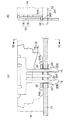
まず、第1実施形態について説明する。図1、図2に示すように、本実施形態に係る固定部材10は、プリント配線基板12に固定される電子部品14に取付け可能になっている。
[First Embodiment]
First, the first embodiment will be described. As shown in FIGS. 1 and 2, the
この固定部材10は、固定部材本体16と、固定部材本体16からアーム状に延びている雄コネクタ部18と、を備えている。雄コネクタ部18の先端には、プリント配線基板12の差込用の開口20に挿入されると開口20の開口縁20Eで係止される爪部19が形成されている。
The
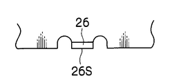
また、プリント配線基板12の開口20の周囲には当接部用はんだランド24Sが形成されており、固定部材本体16には当接部26が曲げ加工によって形成されている。この当接部26には、爪部19が開口縁20Eで係止されると当接部用はんだランド24Sに当接する当接面26Sが形成されている。
A contact
更に、プリント配線基板12には、爪部19の突出側に、爪部19とはんだ接合される爪部用はんだランド24Tが形成されている。そして、当接部用はんだランド24Sと爪部用はんだランド24Tとは同一部材で構成されている。
Further, on the printed
固定部材10を製造するには、板金を所定形状に切断して板状部材を製造し、この板状部材を曲げ加工することによって製造する。その際、図3に示すように、当接部26を形成するための切出し部(延出し部)28を板状部材に形成しておき、この切出し部28に90°の曲げ加工を施すことによって当接部26(図4参照)を形成する。これにより、固定部材10の製造が容易であり、固定部材10の製造時間の短縮を図ることができる。また、板金面によって当接面26Sを形成することができ、面状に加工する工程が不要である。
In order to manufacture the
本実施形態では、電子部品14に固定部材10を取付け、固定部材10の雄コネクタ部18を開口20に挿入し、雄コネクタ部18を爪部19で開口縁20Eに係止させる。そして、爪部19が突出した側からはんだ付けを行う。ここで、当接部用はんだランド24Sと爪部用はんだランド24Tとは同一部材で構成されている。このため、爪部用はんだランド24Tに塗布されたはんだが当接部用はんだランド24Sにまで流れるので、爪部19が爪部用はんだランド24Tに接合されるとともに、当接部26が当接部用はんだランド24Sに接合される。従って、はんだ付けの作業が著しく容易になり、その上、製造時間が短縮される。
In the present embodiment, the
当接部26、爪部用はんだランド24T、及び当接部用はんだランド24Sの寸法は、良好なはんだ接合が得られるように、開口20や雄コネクタ部18の寸法を考慮して予め決めておく。
The dimensions of the
以上説明したように、本実施形態に係る固定部材10では、爪部19と当接部26との両者がはんだ付けでプリント配線基板12に接合されるので、雄コネクタ部18がアーム状であっても雄コネクタ部18が撓むことが規制されている。
As described above, in the
また、固定部材10が電子部品14に取付けられ、上記当接面26Sが当接部用はんだランド24Sにはんだ29で接合されることによって電子部品14がプリント配線基板12に固定された固定構造30を形成している。これにより、撓みを抑制するように固定部材10がプリント配線基板12に固定され得る固定構造30とすることができる。
The
更に、当接部用はんだランド24Sに当接するのは当接部26の当接面26Sであり、面接触しているので、当接部用はんだランド24Sと当接部26との接触状態を著しく良好にすることができる。
Further, the
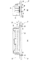
なお、図5、図6に示すような固定部材40を用い、これに合わせた当接部用はんだランド34S及び爪部用はんだランド34Tをプリント配線基板12に形成しておき、電子部品44をプリント配線基板12に固定する形態であってもよい。
5 and 6, the contact portion solder lands 34 </ b> S and the claw portion solder lands 34 </ b> T are formed on the printed
[第2実施形態]
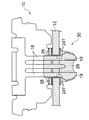
次に、第2実施形態について説明する。図7に示すように、本実施形態に係る固定部材50は、プリント配線基板52に固定される電子部品54に取付け可能になっている。
[Second Embodiment]
Next, a second embodiment will be described. As shown in FIG. 7, the fixing
この固定部材50は、側面が概略L字状であり、電子部品54に取付けられる上部56と、プリント配線基板52に固定される下部57とを有する。そして、電子部品54に取付けられてプリント配線基板52に固定された状態では、固定部材50の下部57がはんだHによってプリント配線基板52にはんだ付けで固定されるようになっている。なお、プリント配線基板52には、下部57をはんだ付けするための下部用はんだランドが形成されている。
The fixing
また、プリント配線基板52には2つの挿通孔60が形成されており、下部57には、挿通孔60にそれぞれ挿通する2つの雄コネクタ部58が突設されている。そして、この2つの雄コネクタ部58には、挿通孔60に挿入されると挿通孔60の開口縁60Eで係止される爪部59がそれぞれ形成されている。
In addition, two
これにより、固定部材50を用いて電子部品54をプリント配線基板52に固定した固定構造70では、下部57がはんだ付けで固定されるとともに、爪部59によって雄コネクタ部58がプリント配線基板52に係止される。従って、固定部材50を大きくすることなく固定強度を従来よりも上げることができる。また、はんだ付け後のプリント配線基板52の撓みが従来よりも抑制される。
Thus, in the fixing
以上、実施形態を挙げて本発明の実施の形態を説明したが、上記実施形態は一例であり、要旨を逸脱しない範囲内で種々変更して実施できる。また、本発明の権利範囲が上記実施形態に限定されないことは言うまでもない。 The embodiments of the present invention have been described with reference to the embodiments. However, the above embodiments are merely examples, and various modifications can be made without departing from the scope of the invention. Needless to say, the scope of rights of the present invention is not limited to the above embodiment.
10 固定部材
12 プリント配線基板
14 電子部品(被固定部材)
18 雄コネクタ部
19 爪部
20 開口
20E 開口縁
24S 当接部用はんだランド
24T 爪部用はんだランド
26 当接部
30 固定構造
34S 当接部用はんだランド
34T 爪部用はんだランド
40 固定部材
44 電子部品(被固定部材)
50 固定部材
52 プリント配線基板
54 電子部品(被固定部材)
58 雄コネクタ部
59 爪部
60 挿通孔(開口)
60E 開口縁
70 固定構造
80 固定部材
82 プリント配線基板
84 電子部品(被固定部材)
88 雄コネクタ部
90 開口
90E 開口縁
99 爪部
DESCRIPTION OF
18
50 fixing
58
88 Male connector part 90 Opening 90E Opening edge 99 Claw part
Claims (4)
アーム状に延び、前記プリント配線基板の差込用の開口に挿入されると前記開口の開口縁で係止される爪部を先端に有する雄コネクタ部と、
前記爪部が前記開口縁で係止されると前記プリント配線基板に形成されているはんだランドに当接し、はんだ付けによって前記はんだランドに接合される当接部と、
が設けられたことを特徴とする固定部材。 A fixing member that can be attached to a fixed member fixed to a printed wiring board, and is used to fix the fixed member to the printed wiring board,
A male connector portion that extends in an arm shape and has a claw portion at the tip that is locked at the opening edge of the opening when inserted into the insertion opening of the printed wiring board;
When the claw portion is locked at the opening edge, it contacts a solder land formed on the printed wiring board, and a contact portion joined to the solder land by soldering;
The fixing member characterized by the above-mentioned.
前記当接面が前記はんだランドにはんだ接合されることによって前記被固定部材が前記プリント配線基板に固定されていることを特徴とする固定構造。 The fixing member according to claim 1 or 2 is attached to the fixed member,
The fixing structure is characterized in that the fixed member is fixed to the printed wiring board by soldering the contact surface to the solder land.
前記プリント配線基板には、前記爪部の突出側に、前記爪部とはんだ接合される爪部用はんだランドが形成され、
前記当接部用はんだランドと前記爪部用はんだランドとが同一部材で構成されていることを特徴とする請求項3に記載の固定構造。 The solder land is a solder land for contact portions arranged around the opening,
In the printed circuit board, a solder land for a nail part to be soldered to the nail part is formed on the protruding side of the nail part,
The fixing structure according to claim 3, wherein the solder land for contact portion and the solder land for claw portion are formed of the same member.
Priority Applications (3)
| Application Number | Priority Date | Filing Date | Title |
|---|---|---|---|
| JP2006013923A JP4805683B2 (en) | 2006-01-23 | 2006-01-23 | Fixing member and fixing structure |
| US11/623,039 US7364460B2 (en) | 2006-01-23 | 2007-01-12 | Fixing member and fixing structure |
| CNB2007100043469A CN100438218C (en) | 2006-01-23 | 2007-01-23 | Fixing member and fixing structure |
Applications Claiming Priority (1)
| Application Number | Priority Date | Filing Date | Title |
|---|---|---|---|
| JP2006013923A JP4805683B2 (en) | 2006-01-23 | 2006-01-23 | Fixing member and fixing structure |
Publications (2)
| Publication Number | Publication Date |
|---|---|
| JP2007200916A true JP2007200916A (en) | 2007-08-09 |
| JP4805683B2 JP4805683B2 (en) | 2011-11-02 |
Family
ID=38286134
Family Applications (1)
| Application Number | Title | Priority Date | Filing Date |
|---|---|---|---|
| JP2006013923A Active JP4805683B2 (en) | 2006-01-23 | 2006-01-23 | Fixing member and fixing structure |
Country Status (3)
| Country | Link |
|---|---|
| US (1) | US7364460B2 (en) |
| JP (1) | JP4805683B2 (en) |
| CN (1) | CN100438218C (en) |
Cited By (2)
| Publication number | Priority date | Publication date | Assignee | Title |
|---|---|---|---|---|
| JP2009259439A (en) * | 2008-04-11 | 2009-11-05 | Tdk-Lambda Corp | Sheet metal with terminal, and connection structure between substrate and sheet metal with terminal |
| JP2017022043A (en) * | 2015-07-14 | 2017-01-26 | 住友電装株式会社 | Connector packaging board |
Families Citing this family (6)
| Publication number | Priority date | Publication date | Assignee | Title |
|---|---|---|---|---|
| JP2007128772A (en) * | 2005-11-04 | 2007-05-24 | Tyco Electronics Amp Kk | Support member, mounting structure, and electronic component |
| CN100508697C (en) * | 2007-08-21 | 2009-07-01 | 无锡荣志电子有限公司 | Technique for placing connectors on printing circuit board |
| TWI453994B (en) * | 2010-04-09 | 2014-09-21 | Hon Hai Prec Ind Co Ltd | Electrical connector |
| JP5236707B2 (en) * | 2010-09-22 | 2013-07-17 | 日立オートモティブシステムズ株式会社 | Electronic equipment control device |
| US8790133B2 (en) * | 2012-10-02 | 2014-07-29 | Tyco Electronics Corporation | Header connector |
| JP6582678B2 (en) * | 2015-07-27 | 2019-10-02 | 三菱電機株式会社 | Semiconductor device |
Citations (6)
| Publication number | Priority date | Publication date | Assignee | Title |
|---|---|---|---|---|
| JPS61156264U (en) * | 1985-03-18 | 1986-09-27 | ||
| JPS6252966U (en) * | 1985-09-24 | 1987-04-02 | ||
| JPS63117064U (en) * | 1987-01-23 | 1988-07-28 | ||
| JPH0257572U (en) * | 1988-10-05 | 1990-04-25 | ||
| JPH07312473A (en) * | 1994-05-18 | 1995-11-28 | Toshiba Fa Syst Eng Kk | Wiring board unit and manufacture of wiring board unit |
| JPH11273797A (en) * | 1998-03-23 | 1999-10-08 | Harness Syst Tech Res Ltd | Connector structure of electric connecting box |
Family Cites Families (9)
| Publication number | Priority date | Publication date | Assignee | Title |
|---|---|---|---|---|
| JPH0479507A (en) * | 1990-07-20 | 1992-03-12 | Amp Japan Ltd | Filter and electric connector with filter |
| JP2890933B2 (en) * | 1991-12-09 | 1999-05-17 | 株式会社村田製作所 | connector |
| US5186634A (en) * | 1991-12-20 | 1993-02-16 | John Fluke Mfg. Co., Inc. | Electrical contact having spring-biased tabs for mounting to a circuit board |
| US6095872A (en) | 1998-10-21 | 2000-08-01 | Molex Incorporated | Connector having terminals with improved soldier tails |
| TW430174U (en) * | 1999-02-02 | 2001-04-11 | Hon Hai Prec Ind Co Ltd | Electrical connector |
| CN2454931Y (en) * | 2000-11-08 | 2001-10-17 | 富士康(昆山)电脑接插件有限公司 | Electric connector |
| US6454588B1 (en) * | 2001-12-13 | 2002-09-24 | Hon Hai Precision Ind. Co., Ltd. | Contact of socket connector |
| US6638106B1 (en) * | 2002-09-27 | 2003-10-28 | Hon Hai Precision Ind. Co., Ltd. | Multi-port electrical connector having improved board locks |
| JP4007970B2 (en) * | 2004-03-30 | 2007-11-14 | 日本航空電子工業株式会社 | Connector fixing member and connector using the same |
-
2006
- 2006-01-23 JP JP2006013923A patent/JP4805683B2/en active Active
-
2007
- 2007-01-12 US US11/623,039 patent/US7364460B2/en active Active
- 2007-01-23 CN CNB2007100043469A patent/CN100438218C/en active Active
Patent Citations (6)
| Publication number | Priority date | Publication date | Assignee | Title |
|---|---|---|---|---|
| JPS61156264U (en) * | 1985-03-18 | 1986-09-27 | ||
| JPS6252966U (en) * | 1985-09-24 | 1987-04-02 | ||
| JPS63117064U (en) * | 1987-01-23 | 1988-07-28 | ||
| JPH0257572U (en) * | 1988-10-05 | 1990-04-25 | ||
| JPH07312473A (en) * | 1994-05-18 | 1995-11-28 | Toshiba Fa Syst Eng Kk | Wiring board unit and manufacture of wiring board unit |
| JPH11273797A (en) * | 1998-03-23 | 1999-10-08 | Harness Syst Tech Res Ltd | Connector structure of electric connecting box |
Cited By (2)
| Publication number | Priority date | Publication date | Assignee | Title |
|---|---|---|---|---|
| JP2009259439A (en) * | 2008-04-11 | 2009-11-05 | Tdk-Lambda Corp | Sheet metal with terminal, and connection structure between substrate and sheet metal with terminal |
| JP2017022043A (en) * | 2015-07-14 | 2017-01-26 | 住友電装株式会社 | Connector packaging board |
Also Published As
| Publication number | Publication date |
|---|---|
| US20070173134A1 (en) | 2007-07-26 |
| JP4805683B2 (en) | 2011-11-02 |
| CN101009408A (en) | 2007-08-01 |
| CN100438218C (en) | 2008-11-26 |
| US7364460B2 (en) | 2008-04-29 |
Similar Documents
| Publication | Publication Date | Title |
|---|---|---|
| JP4805683B2 (en) | Fixing member and fixing structure | |
| JP2005317701A (en) | Structure for connecting flexible printed board to printed board | |
| JP4626680B2 (en) | Holding member, electronic component, and electronic device | |
| JP2012033435A (en) | Fitting fixture for component mounted on circuit board | |
| JP4560727B2 (en) | Board connector | |
| JP6943959B2 (en) | Electronic circuit board | |
| JP2007141592A (en) | Connector | |
| JP2006031944A (en) | Surface mounting connector | |
| JP4020149B1 (en) | Electronic component module | |
| JP4797781B2 (en) | Reinforcing tab, reinforcing tab manufacturing method, and connector mounting structure | |
| JP5293688B2 (en) | Holding member | |
| JP2010258190A (en) | Connection body for printed board | |
| JP7050718B2 (en) | Positioning jig for soldering | |
| JP2007059679A (en) | Printed wiring board | |
| JP2012129491A (en) | Connection structure of printed circuit board and connection method therefor | |
| JP2009064911A (en) | Electronic circuit module | |
| JP2007005225A (en) | Connector fixing structure | |
| JP4844260B2 (en) | Electronic component and manufacturing method thereof | |
| JP2007165252A (en) | Electric connector | |
| JP2006237176A (en) | Connection structure of printed circuit board | |
| JP2006108436A (en) | Connection structure of printed wiring board | |
| JP2019047032A (en) | Printed board | |
| JP2008217995A (en) | Board terminal aligning plate and board mounting connector | |
| JP2006310567A (en) | Electronic component for reflow soldering | |
| JP2008066332A (en) | Printed-circuit board |
Legal Events
| Date | Code | Title | Description |
|---|---|---|---|
| A621 | Written request for application examination |
Free format text: JAPANESE INTERMEDIATE CODE: A621 Effective date: 20080523 |
|
| A977 | Report on retrieval |
Free format text: JAPANESE INTERMEDIATE CODE: A971007 Effective date: 20101101 |
|
| A131 | Notification of reasons for refusal |
Free format text: JAPANESE INTERMEDIATE CODE: A131 Effective date: 20101109 |
|
| A521 | Request for written amendment filed |
Free format text: JAPANESE INTERMEDIATE CODE: A523 Effective date: 20110111 |
|
| TRDD | Decision of grant or rejection written | ||
| A01 | Written decision to grant a patent or to grant a registration (utility model) |
Free format text: JAPANESE INTERMEDIATE CODE: A01 Effective date: 20110809 |
|
| A01 | Written decision to grant a patent or to grant a registration (utility model) |
Free format text: JAPANESE INTERMEDIATE CODE: A01 |
|
| A61 | First payment of annual fees (during grant procedure) |
Free format text: JAPANESE INTERMEDIATE CODE: A61 Effective date: 20110811 |
|
| R150 | Certificate of patent or registration of utility model |
Ref document number: 4805683 Country of ref document: JP Free format text: JAPANESE INTERMEDIATE CODE: R150 Free format text: JAPANESE INTERMEDIATE CODE: R150 |
|
| FPAY | Renewal fee payment (event date is renewal date of database) |
Free format text: PAYMENT UNTIL: 20140819 Year of fee payment: 3 |
|
| R250 | Receipt of annual fees |
Free format text: JAPANESE INTERMEDIATE CODE: R250 |
|
| R250 | Receipt of annual fees |
Free format text: JAPANESE INTERMEDIATE CODE: R250 |
|
| R250 | Receipt of annual fees |
Free format text: JAPANESE INTERMEDIATE CODE: R250 |
|
| R250 | Receipt of annual fees |
Free format text: JAPANESE INTERMEDIATE CODE: R250 |
|
| R250 | Receipt of annual fees |
Free format text: JAPANESE INTERMEDIATE CODE: R250 |
|
| R250 | Receipt of annual fees |
Free format text: JAPANESE INTERMEDIATE CODE: R250 |
|
| R250 | Receipt of annual fees |
Free format text: JAPANESE INTERMEDIATE CODE: R250 |
|
| R250 | Receipt of annual fees |
Free format text: JAPANESE INTERMEDIATE CODE: R250 |
|
| R250 | Receipt of annual fees |
Free format text: JAPANESE INTERMEDIATE CODE: R250 |