JP2007200626A - Organic electroluminescent element - Google Patents
Organic electroluminescent element Download PDFInfo
- Publication number
- JP2007200626A JP2007200626A JP2006015670A JP2006015670A JP2007200626A JP 2007200626 A JP2007200626 A JP 2007200626A JP 2006015670 A JP2006015670 A JP 2006015670A JP 2006015670 A JP2006015670 A JP 2006015670A JP 2007200626 A JP2007200626 A JP 2007200626A
- Authority
- JP
- Japan
- Prior art keywords
- organic
- layer
- light emitting
- transparent electrode
- electrode
- Prior art date
- Legal status (The legal status is an assumption and is not a legal conclusion. Google has not performed a legal analysis and makes no representation as to the accuracy of the status listed.)
- Withdrawn
Links
Images


Abstract
Description
本発明は、有機EL素子に係り、詳しくは、透明電極とその対向電極の間に挟持された有機発光層を含む有機EL層の膜厚分布に起因した発光ムラを低減する有機EL素子に関する。 The present invention relates to an organic EL element, and more particularly to an organic EL element that reduces light emission unevenness due to a film thickness distribution of an organic EL layer including an organic light emitting layer sandwiched between a transparent electrode and a counter electrode.
近年、有機薄膜のエレクトロルミネセンス(EL)現象を利用して、透明電極を含む一対の電極間に有機発光層を含有する有機EL層を挟み、その電極間に電圧を印加し有機EL層に電流を流して発光させる有機EL素子は、その高性能化に向けた検討が精力的に進められている。この有機EL素子は、フラットパネルディスプレイ(FPD;Flat Panel Display)あるいは有機LED(Light Emitting Diode)のような表示装置、非自発光素子で成る液晶表示装置の面光源バックライトあるいは照明灯のような照明装置に好適な自発光素子である。以下、この有機EL素子を用いた表示装置および照明装置を有機EL発光装置と総称する。 In recent years, by utilizing the electroluminescence (EL) phenomenon of an organic thin film, an organic EL layer containing an organic light emitting layer is sandwiched between a pair of electrodes including a transparent electrode, and a voltage is applied between the electrodes to form an organic EL layer. With respect to organic EL elements that emit light by passing an electric current, studies for improving the performance thereof are energetically advanced. The organic EL element is a display device such as a flat panel display (FPD) or an organic LED (Light Emitting Diode), or a surface light source backlight or a illuminating lamp of a liquid crystal display device including a non-self light emitting element. It is a self-luminous element suitable for a lighting device. Hereinafter, a display device and an illumination device using the organic EL element are collectively referred to as an organic EL light emitting device.
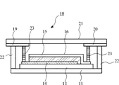
以下に従来の有機EL素子が適用された有機EL発光装置について、図8,9を参照して説明する。図8は上記従来の有機EL発光装置の構造の一例を示す模式的な断面図であり、図9は有機発光層の膜厚分布の一例を示す膜厚マップ図である。 Hereinafter, an organic EL light emitting device to which a conventional organic EL element is applied will be described with reference to FIGS. FIG. 8 is a schematic cross-sectional view showing an example of the structure of the conventional organic EL light emitting device, and FIG. 9 is a film thickness map showing an example of the film thickness distribution of the organic light emitting layer.
図8に示すように、有機EL発光装置100では、透明ガラス基板101上に例えばAl(アルミニウム)の金属材料により、第1の電極取り出し配線102および第2の電極取り出し配線103が形成されている。そして、例えば透光性材料のITO(インジウム錫酸化物)等により透明電極104が形成される。更に、上記透明電極104上に膜厚が100nm〜300nm程度になる有機EL層105が形成され、この有機EL層105を挟んで例えばAl金属から成る対向電極106が形成されている。
As shown in FIG. 8, in the organic EL
ここで、上記有機EL層105は、例えば4,4’−ビス[N−(2−ナフチル)−N−フェニル−アミノ]ビフェニル(α−NPDとも言う)から成る正孔輸送層、例えばトリス(8−キノリノラト)アルミニウム錯体(Alq3とも言う)のような有機発光層の電子輸送性発光層、および極薄(1nm程度)の電子注入層から成る。この電子注入層は、通常、仕事関数の小さい(例えば3eV以下)、アルカリ金属、アルカリ土類金属、これ等金属の合金、上記金属のハロゲン化合物、あるいは、これ等の金属と有機物の混合層により形成される。
Here, the
そして、透明電極104は第1の電極取り出し配線102を通して電源に接続するようになっており、上記対向電極106は第2の電極取り出し配線103を通して別の電源につながっている。また、接着剤107による接合を通して、ガラス製あるいはステンレス製であって非透湿性の封止缶108により全体が気密封止されている。
The
上記有機EL発光装置100において、透明電極104、有機EL層105および対向電極106により有機EL素子が構成される。そして、有機発光層である電子輸送性発光層に生じるEL光が透明ガラス基板101から出射する。ここで、有機EL層105は、特に酸素あるいは水分によって劣化し易いことから、上記封止缶108による気密封止が必要になる。図示していないが、この酸素ガスあるいは水分等を吸着するように、更に封止缶108内に例えば酸化バリウム粉末等の乾燥剤が封入される。
In the organic EL
また、上記有機EL層105は、透明電極104上における膜厚のバラツキが不可避である。図9は、通常の真空蒸着法により成膜される有機発光層である電子輸送性発光層の膜厚バラツキの一例である。例えば発光面が5cm×5cmの正方形パターンにおいて、その中央部の膜厚を100%とすると、その周辺に行くに従い膜厚は98%、96%および94%と薄くなっていく。そして、上記パターンの角隅部における膜厚は92%程度になる。このように、真空蒸着法により成膜される有機発光層あるいは正孔輸送層のような有機材料膜は通常において発光面内で+/−5%程度の膜厚分布を有し、有機EL層105も同程度の膜厚バラツキを有することになる。
Further, the
ここで、上記有機EL素子の高性能化において、発光の高輝度化、高効率化あるいは発光面の面積の増大化が進んでくると、上記有機EL層の膜厚分布、例えば有機発光層の膜厚分布に起因した発光ムラ(輝度ムラ、色ムラ)の問題が顕在化してくる。そして、有機EL素子における駆動の低電圧化のために有機EL層の膜厚が薄くなると共に、発光素子内での有機EL層の僅かな膜厚バラツキによって顕著な発光面の輝度ムラあるいは色ムラが生じるようになってくる。 Here, in the enhancement of the performance of the organic EL element, when the luminance of light emission is increased, the efficiency is increased, or the area of the light emitting surface is increased, the film thickness distribution of the organic EL layer, for example, of the organic light emitting layer is increased. The problem of light emission unevenness (brightness unevenness, color unevenness) due to the film thickness distribution becomes obvious. In addition, the organic EL layer is thinned to reduce the driving voltage in the organic EL element, and the luminance unevenness or color unevenness of the light emitting surface due to slight film thickness variation of the organic EL layer in the light emitting element. Comes to occur.
本発明は、上述の事情に鑑みてなされたものであって、有機EL素子における有機EL層の膜厚分布に起因する発光ムラを簡便に低減させることのできる有機EL素子を提供することを目的とする。 The present invention has been made in view of the above-described circumstances, and an object thereof is to provide an organic EL element that can easily reduce light emission unevenness due to the film thickness distribution of an organic EL layer in an organic EL element. And
上記目的を達成するために、本発明の有機EL素子は、少なくとも有機発光層を含む有機EL層と、該有機EL層を挟持する透明電極およびその対向電極と、を有する構造の複数の有機EL素子が一基板上に張り付けられ、前記複数の有機EL素子により構成された発光面における輝度ムラが低減するように、前記基板上において前記複数の有機EL素子が配置されている、構成になっている。 In order to achieve the above object, the organic EL device of the present invention includes a plurality of organic EL elements having a structure having at least an organic EL layer including an organic light emitting layer, a transparent electrode sandwiching the organic EL layer, and a counter electrode thereof. The plurality of organic EL elements are arranged on the substrate so that the element is attached on one substrate and the luminance unevenness on the light emitting surface composed of the plurality of organic EL elements is reduced. Yes.
上記発明において、前記複数の有機EL素子において膜厚分布を有する前記有機EL層の膜厚の薄くなる領域が前記一基板上の中央部に位置するように、前記複数の有機EL素子が配置される。 In the above invention, the plurality of organic EL elements are arranged such that a region where the thickness of the organic EL layer having a film thickness distribution in the plurality of organic EL elements is thin is located at a central portion on the one substrate. The
そして、好適な一態様では、前記複数の有機EL素子は、少なくとも有機発光層を含む有機EL層と、該有機EL層を挟持する透明電極およびその対向電極とを有する1個の有機EL素子が切断され分割されたものである。ここで、前記1個の有機EL素子は、前記有機EL層の厚さに前記透明電極の厚さを加算した厚さが前記1個の有機EL素子の発光面において均一になるように形成されていると更に好ましい。 In a preferred embodiment, the plurality of organic EL elements include an organic EL layer including at least an organic light emitting layer, a transparent electrode sandwiching the organic EL layer, and a counter electrode thereof. It has been cut and divided. Here, the one organic EL element is formed such that the thickness obtained by adding the thickness of the transparent electrode to the thickness of the organic EL layer is uniform on the light emitting surface of the one organic EL element. More preferably.
上記発明により、有機EL層が膜厚分布を有しその膜厚が発光の面内で大きくばらつくことがあっても、有機EL素子における発光面の輝度ムラおよび色ムラを簡便に低減させることができる。そして、有機EL素子における有機EL層の薄膜化あるいは発光面の面積の増大化が容易になる。 According to the above invention, even when the organic EL layer has a film thickness distribution and the film thickness varies greatly in the plane of light emission, it is possible to easily reduce luminance unevenness and color unevenness of the light emitting surface in the organic EL element. it can. And it becomes easy to make the organic EL layer thinner or increase the area of the light emitting surface in the organic EL element.
あるいは、本発明の有機EL素子は、少なくとも有機発光層を含む有機EL層と、該有機EL層を挟持する透明電極および対向電極とを有する有機EL素子であって、前記有機EL層の厚さに前記透明電極の厚さを加算した厚さが前記有機EL素子の発光面において均一になるように形成されている、構成になっている。 Alternatively, the organic EL element of the present invention is an organic EL element having at least an organic EL layer including an organic light emitting layer, and a transparent electrode and a counter electrode sandwiching the organic EL layer, and the thickness of the organic EL layer Further, the thickness obtained by adding the thickness of the transparent electrode to the light emitting surface of the organic EL element is uniform.
上記発明において、膜厚分布を有する前記有機EL層の膜厚が厚くなる領域に、前記透明電極よりシート抵抗の小さい補助電極が前記透明電極に電気接続して配設される。 In the above invention, in the region where the film thickness of the organic EL layer having a film thickness distribution is increased, an auxiliary electrode having a sheet resistance smaller than that of the transparent electrode is electrically connected to the transparent electrode.
上記発明により、有機EL発光装置において、低抵抗の補助電極が有機EL層を流れる電流値を調整するようになる。そして、有機EL層の発光輝度は上記電流値に強く依存することから、上記補助電極による抵抗調整により上記有機EL素子の発光面の色ムラと共に輝度ムラが低減する。 According to the above invention, in the organic EL light emitting device, the value of the current flowing through the organic EL layer by the low-resistance auxiliary electrode is adjusted. Since the light emission luminance of the organic EL layer strongly depends on the current value, the luminance unevenness is reduced together with the color unevenness of the light emitting surface of the organic EL element by adjusting the resistance by the auxiliary electrode.
本発明の構成によれば、有機EL素子における有機EL層の膜厚分布に起因する発光面の発光ムラが簡便に低減される。 According to the structure of this invention, the light emission nonuniformity of the light emission surface resulting from the film thickness distribution of the organic EL layer in an organic EL element is reduced easily.
以下、本発明の好適な実施形態のいくつかを図面を参照して説明する。この図面では、互いに同一または類似の部分には共通の符号を付す。
(実施の形態1)
本発明の第1の実施形態について図1ないし5を参照して説明する。この実施形態では、本発明の有機EL素子を備えた有機EL発光装置について説明する。図1はこの有機EL発光装置の封止缶を除いたところの概略平面図である。そして、図2は有機EL発光装置の断面図である。
Several preferred embodiments of the present invention will be described below with reference to the drawings. In this drawing, the same or similar parts are denoted by common reference numerals.
(Embodiment 1)
A first embodiment of the present invention will be described with reference to FIGS. In this embodiment, an organic EL light emitting device including the organic EL element of the present invention will be described. FIG. 1 is a schematic plan view of the organic EL light emitting device excluding the sealing can. FIG. 2 is a cross-sectional view of the organic EL light emitting device.
図1に示すように、有機EL発光装置10では、例えば透明ガラス基板11上に4個の集積した有機EL素子12が張り付けられている。この集積した有機EL素子12は、第1の有機EL素子12a、第2の有機EL素子12b、第3の有機EL素子12cおよび第4の有機EL素子12dから構成される。そして、第1の有機EL素子12aには、例えば透光性材料から成る基材13a上に透光性材料から成る透明電極14a、有機EL層15aおよび対向電極16aがこの順に積層して形成してある。同様にして、第2の有機EL素子12bには、透光性材料から成る基材13b上に透明電極14b、有機EL層15bおよび対向電極16bが積層して形成してある。また、第3の有機EL素子12cには、透光性材料から成る基材13c上に透明電極14c、有機EL層15cおよび対向電極16cが積層して形成してある。更に、第4の有機EL素子12dには、透光性材料から成る基材13d上に透明電極14d、有機EL層15dおよび対向電極16dが積層して形成してある。
As shown in FIG. 1, in the organic EL
そして、上記第1の有機EL素子12a、第2の有機EL素子12b、第3の有機EL素子12cおよび第4の有機EL素子12dは、図1に示すように、第1の縁端17と第2の縁端18において互いに結合し、上述したように透明ガラス基板11に張り付けられている。このようにして、集積した有機EL素子12は、上記基材13a、13b、13c、13dの集積する基材13、上記透明電極14a、14b、14c、14dの集積する透明電極14、上記有機EL層15a、15b、15c、15dの集積する有機EL層15、および上記対向電極16a、16b、16c、16dの集積する対向電極16から成り、その発光面の面積が拡張した有機EL素子となる。
The first
図2に示すように、この面積拡張する集積した有機EL素子12から成る有機EL発光装置10では、透明ガラス基板11上に上記集積する基材13が張り付けて形成され、更に、この基材13上に上記集積する透明電極14が形成され、この集積する透明電極14上に有機発光層を含み集積する有機EL層15が積層されている。そして、この有機EL層15上に上記透明電極14に対向して集積する対向電極16が設けられている。
As shown in FIG. 2, in the organic EL light-emitting
そして、第1の電極取り出し配線19および第2の電極取り出し配線20が配設され、絶縁材料から成る封止部材21が、例えばUV硬化樹脂22により透明ガラス基板11に接合され全体を気密封止している。ここで、上記透明電極14は、例えば接続部材23により第1の電極取り出し配線19に電気接続している。同様に、上記対向電極16は、接続部材23により第2の電極取り出し配線20に電気接続している。
Then, the first electrode lead-
このような有機EL発光装置10において、上記基材13は例えば厚さが0.5mm以下の石英ガラスから成る。そして、上記透明電極14は例えば厚さが150nm程度のITO、ZnO(酸化亜鉛)のような透光性材料から成る。また、上記有機EL層15は、従来の技術で説明したのと同様に、例えばα−NPDの正孔輸送層、Alq3の電子輸送性発光層および電子注入層から成る。そして、その積層した全膜厚は100nm以下であり、この有機EL発光装置では、5V以下の低電圧駆動が可能となる。
In such an organic EL
その他に、上記有機EL層15は、有機発光層のみの単層であってもよい。また、この有機EL層15は、正孔注入層、正孔輸送層、正孔阻止層、電子注入層、電子輸送層、電子阻止層の一層以上と有機発光層との積層した多層構造であってもよい。更には、複数の有機EL層を中間導電層を介して積層させる、マルチフォトンエミッション(MPE;Multi-Photo-Emission)といわれる構造になっていてもよい。この場合は、有機EL素子の高輝度化が容易になる。なお、上記集積した有機EL素子12における有機EL層15は正方形パターン(矩形パターン)になっているが、他の形状パターン例えば円形パターンに形成されていてもよい。
In addition, the
そして、上記対向電極16は、透光性材料により形成することは必要でなく、例えば膜厚が150nm程度のAl金属膜により形成される。また、上記封止部材21は、例えば非透湿性ガラスから成り、特に酸素あるいは水分によって劣化し易い有機EL素子12を気密封止する。あるいは、図示しないが、封止部材21内には、例えば酸化バリウム粉末等の乾燥剤が封入され、酸素ガスあるいは水分等を吸着するようになっている。
The
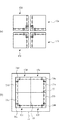
次に、上記有機EL発光装置10の製造方法について、図1、図2、および図3、図4を参照して説明する。図3は有機EL発光装置の製造方法を示す製造工程別平面図である。そして、図4は図3に引き続く製造工程別平面図である。ここで、図中において成膜したパターンを明確にするために斜線が施されている。
Next, a method for manufacturing the organic EL
上記製造方法では、例えば板厚は0.5mm程度の石英ガラスの基材13を洗浄した後に、例えばスパッタリング法によりITOのような透光性金属材料を全面に成膜する。そして、公知のフォトリソグラフィとウェットエッチングにより上記成膜したITO膜を所定の斜線を施したようなパターンに加工する。このようにして、図3(a)に示すように、基材13上に透明電極14を形成する。
In the above manufacturing method, for example, after a
次に、有機物成膜用金属マスクを用いた真空蒸着法により、図3(b)に示すように、透明電極14上に斜線を施すパターンの有機EL層15を形成する。ここで、上記有機EL層15の形成では、例えば膜厚が60nm程度の正孔輸送層と40nm程度の電子輸送性発光層を連続して成膜する。そして、上記電子輸送性発光層上に膜厚が0.5nm程度の電子注入層を成膜し有機EL層15とする。ここで、有機EL層15の正孔輸送層、電子輸送性発光層および電子注入層は、同じ真空蒸着装置内において、例えばα−NPD入りの抵抗加熱ボート、Alq3入りの抵抗加熱ボート、金属LiあるいはLiF等の蒸着源をそれぞれ順番に加熱して成膜される。上記有機EL層15の成膜においては、その膜厚分布が図9に説明したように中央部で厚く周辺部で薄くなる。
Next, as shown in FIG. 3B, the
次に、図3(c)に示すように、金属物成膜用金属マスクを用いたスパッタリング法により、上記有機EL層15上に斜線を施したパターンのAl金属膜から成る対向電極16を形成する。ここで、Al金属膜の成膜は、上記真空蒸着装置に連結したスパッタリング装置内において、Alスパッタリングターゲットを用いAr(アルゴン)雰囲気で行われる。
Next, as shown in FIG. 3C, a
次に、図4(a)に示すように、図3(c)状態の基材13を例えばスクライバーにより十文字に切断して分割する。このようにして4個から成る第1の有機EL素子12a、第2の有機EL素子12b、第3の有機EL素子12c、第4の有機EL素子12dを形成する。この切断においては、積層する透明電極13、有機EL層15および対向電極16の接合部における損傷を生じさせないようにすることが極めて重要である。
Next, as shown in FIG. 4A, the
次に、図4(b)に示すように、上記切断し分離・分割した第1の有機EL素子12a、第2の有機EL素子12b、第3の有機EL素子12c、第4の有機EL素子12dをそれぞれに並べ替えて透明ガラス基板11上に配置する。そして、これ等の有機EL素子を第1の縁端17および第2の縁端18において結合させ、透明な接着剤により透明ガラス基板11表面に張り付ける。このようにして、図1で説明した集積した有機EL素子12が透明ガラス基板11上に形成される。
Next, as shown in FIG. 4B, the first
このようにした後に、図4(b)に示した透明電極パッド24a、24b、24c、24dおよび対向電極パッド25a、25b、25c、25dのそれぞれに図2に示した接続部材23を配置する。ここで、接続部材23は、例えば低融点の半田ボールバンプあるいは例えばバネのような弾性のある導電体により構成される。更に、図2に示すように透明ガラス基板11の縁端部にUV硬化樹脂22を塗布する。
After this, the
そして、上記UV硬化樹脂22を介して、図2に示した封止部材21、第1の電極取り出し配線19および第2の電極取り出し配線20の表面を透明ガラス基板11に接合させる。また、上記接続部材23を介して、第1の電極取り出し配線19と透明電極パッド24a、24b、24c、24dを接続させる。同様に、第2の電極取り出し配線20と対向電極パッド25a、25b、25c、25dを接続させる。ここで、UV光が有機EL層15を照射しないようにしてUV硬化樹脂22をUVキュアーする。
Then, the surfaces of the sealing
このようにして、例えば非透湿性ガラスから成る封止部材21により、図2に示したように全体を気密封止する。ここで、図示しないが、封止部材21内面には、予め例えば酸化バリウム粉末等の乾燥剤を取り付けておき、酸素ガスあるいは水分等が吸着されるようする。
In this manner, the whole is hermetically sealed as shown in FIG. 2 by the sealing
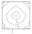
次に、図5を参照して上記有機EL発光装置10における発光面の輝度ムラについて説明する。図5は、横軸に図1で説明した正方形パターンの集積した有機EL層15上の中央部から角隅部にわたる径をとり、縦軸に上記発光装置の相対的輝度をとっている。ここで、最外部の角隅の輝度を1とした。また、比較対象とした従来技術の有機EL素子を用いた有機EL発光装置は図8に示した従来の構造にし、有機EL層105は図9に示したように全面に成膜されている。そして、上記有機EL層105の成膜、透明電極104および対向電極106の成膜は、上記実施形態の場合と同じ真空蒸着装置およびスパッタリング装置において同一条件に行っている。更に、透明ガラス基板101の厚さが本実施形態の透明ガラス基板11と基材13の厚さと同じになるようにしている。
Next, the luminance unevenness of the light emitting surface in the organic EL
図5において、本実施形態の場合には、最も輝度の高くなる角隅部に対して、中央部の相対輝度は0.8程度になり、集積した有機EL層15上での発光面の輝度ムラは大きく向上するようになる。これに対して、比較対象にした図5で説明した従来技術の場合には、同様に最も輝度の高くなる角隅部に対する中央部の相対輝度は0.4程度である。図1に示した本実施形態の集積した有機EL素子における効果は、図3、図4で説明したように有機EL素子の切断/分割とその再配列により生じる。
In FIG. 5, in the case of the present embodiment, the relative luminance of the central portion is about 0.8 with respect to the corner portion where the luminance is highest, and the luminance of the light emitting surface on the integrated
第1の実施形態では、有機EL層15の成膜で生じる膜厚分布において膜厚の薄くなる領域が、上記集積した有機EL素子12の中央部に配置され、膜厚の厚くなる領域が上記集積した有機EL素子12の周辺部である角隅部に配置される。このようにして、複数個の集積した有機EL素子における発光面の発光の輝度ムラは大きく低減するようになる。この効果は、有機EL層の薄膜化あるいは発光面の面積の増大化において顕著になってくる。
In the first embodiment, in the film thickness distribution generated by the film formation of the
図3、図4で説明した集積した有機EL素子は、一度作製した有機EL素子が切断/分割され発光ムラの低減するように再配列されて製造されるが、図1に示した集積した有機EL素子はこのような製造方法に限定されるものではない。第1の有機EL素子12a、第2の有機EL素子12b、第3の有機EL素子12c、第4の有機EL素子12dをそれぞれ別々の工程を通して作製してからこれ等の有機EL素子を一基板上に配置し張り付け集積するようにしてもよい。また、集積する有機EL素子は4個に限らない複数個であってもよい。
The integrated organic EL elements described with reference to FIGS. 3 and 4 are manufactured by cutting / dividing the once manufactured organic EL elements and rearranging them so as to reduce light emission unevenness. However, the integrated organic EL elements shown in FIG. The EL element is not limited to such a manufacturing method. The first
(実施の形態2)
次に、本発明の第2の実施形態について図6、図7を参照して説明する。本実施形態は、特に有機EL層の膜厚分布に起因して生じる発光面における発光の色ムラを効果的に低減させることを特徴とする。ここで、具体的には、有機EL素子において有機EL層の膜厚分布にあわせて透明電極の膜厚を調整する。図6はこの有機EL素子を備える有機EL発光装置の断面図であり、図7はその変形例となる有機EL発光装置の平面図である。
(Embodiment 2)
Next, a second embodiment of the present invention will be described with reference to FIGS. The present embodiment is characterized in that color unevenness of light emission on the light emitting surface caused by the film thickness distribution of the organic EL layer is effectively reduced. Here, specifically, the film thickness of the transparent electrode is adjusted in accordance with the film thickness distribution of the organic EL layer in the organic EL element. FIG. 6 is a cross-sectional view of an organic EL light-emitting device including the organic EL element, and FIG. 7 is a plan view of an organic EL light-emitting device that is a modification thereof.
図6に示すように、有機EL発光装置30では、透明ガラス基板11上に例えばAl金属材料により、第1の電極取り出し配線31および第2の電極取り出し配線32が形成されている。そして、例えばITOから成る透明電極33が形成されている。ここで、透明電極33の中央部の領域で膜厚が薄くその周辺部で膜厚が厚くなっている。更に、上記透明電極33上に有機EL層34が形成され、この有機EL層34を挟んで例えばAl金属から成る対向電極35が形成されている。
As shown in FIG. 6, in the organic EL
ここで、上記有機EL層34は、例えばα−NPDから成る正孔輸送層、Alq3のような有機発光層の電子輸送性発光層および電子注入層から成る。この有機EL層34は、第1の実施形態で説明した真空蒸着法およびスパッタリング法により成膜され、図9で説明したようにその中央部で膜厚が厚く周辺部で薄くなる。上記互いに逆の膜厚分布を有する透明電極33と有機EL層34とを積層することにより、これら積層した膜の膜厚分布が発光面において一様になる。このようにすることにより、光の干渉に伴う有機EL素子の色ムラが大幅に低減するようになる。
Here, the
そして、透明電極33は第1の電極取り出し配線31を通して電源に接続し、対向電極35は第2の電極取り出し配線32を通して別の電源につながっている。また、UV硬化樹脂22による接合を通して、非透湿性ガラス製あるいはステンレス製の封止部材21により全体が気密封止されている。そして、図示していないが、この酸素ガスあるいは水分等を吸着するように、更に封止部材21内に例えば酸化バリウム粉末等の乾燥剤が封入される。
The
上記有機EL発光装置30において、有機EL層34は、有機発光層のみの単層であってもよい。あるいは、正孔注入層、正孔輸送層、正孔阻止層、電子注入層、電子輸送層、電子阻止層の一層以上と有機発光層との積層した多層になる構造であってもよい。更には、複数の有機EL層を中間導電層を介して積層させる、MPEの構造になっていてもよい。
In the organic EL
次に、図7に示す変形例である有機EL発光装置40では、例えば透明ガラス基板11上に、図6で説明したような透明電極33が形成される。ここで、上述したように透明電極33の中央部の領域で膜厚が薄くその周辺部で膜厚が厚くなっている。そして、所定パターンの補助電極36が、透明電極33よりも抵抗率の小さい金属材料によって、透明電極33上に電気接続して配設されている。更に、上記補助電極36を被覆する層間絶縁層(不図示)が設けられ、透明電極33上に有機EL層34が積層されている。そして、上記有機EL層34上に透明電極33に対向して対向電極35が設けられている。
Next, in the organic EL
一般的に、透光性材料から成る透明電極はその導電率が充分に大きくないために、有機EL発光装置において電源から近い部分と遠い部分で電流パスの抵抗値の差が大きくなり、有機EL層の電流値についても発光面上の場所による差が大きくなる。そして、有機EL層の発光輝度が上記電流値に強く依存することから、有機EL素子においてその発光の輝度ムラが生じ易くなっていた。しかし、上述したような低抵抗の補助電極36の配設により、上記有機EL素子の発光の色ムラと共に輝度ムラも低減するようになる。
In general, since the conductivity of a transparent electrode made of a translucent material is not sufficiently large, the difference in resistance value of the current path between the portion near and far from the power source in the organic EL light-emitting device becomes large, and the organic EL The difference in the current value of the layer also depends on the location on the light emitting surface. Since the light emission luminance of the organic EL layer strongly depends on the current value, the luminance unevenness of the light emission is likely to occur in the organic EL element. However, the provision of the low-
更に、上記補助電極36は第1の電極取り出し端子36aを通して一電源に接続するようになっている。同様に、上記対向電極35の端部が第2の電極取り出し端子として他電源につながるようになっている。そして、二点鎖線で記した封止部材21により全体が気密封止されている。
Further, the
第2の実施形態では、有機EL層34の膜厚分布に対応して透明電極33の膜厚分布を調整する。そして、これ等の積層した膜の膜厚が発光面において均一になるようにする。あるいは、透明電極33パターンの中央部にシート抵抗の小さな補助電極36を配設し接続させる。このようにすることにより、有機EL素子における有機EL層に膜厚分布が生じても、その発光面における発光ムラである発光の色ムラおよび輝度ムラが大幅に低減するようになる。
In the second embodiment, the film thickness distribution of the
本発明の実施形態は、その他に、上記第1の実施形態と第2の実施形態を組み合わせた態様であってもよい。この場合には、第2の実施形態の図6で説明した1個の有機EL素子を図3および図4に示したように切断/分割し複数の有機EL素子にした後にこれ等の有機EL素子を同一基板に再配列し張り付ける。ここで、図3および図4に示した製造工程において、図3(a)の透明電極13の成膜は、図6において説明したように、透明電極13に積層する有機EL層15の膜厚分布と逆の膜厚分布を有するように行う。そして、上記互いに逆の膜厚分布を有する透明電極13と有機EL層15とを積層することにより、これら積層した膜の膜厚分布が発光面において均一になるようにする。
In addition, the embodiment of the present invention may be a mode in which the first embodiment and the second embodiment are combined. In this case, one organic EL element described in FIG. 6 of the second embodiment is cut / divided into a plurality of organic EL elements as shown in FIG. 3 and FIG. The elements are rearranged and pasted on the same substrate. Here, in the manufacturing process shown in FIGS. 3 and 4, the film formation of the
このようにすることにより、有機EL層の膜厚分布を有する有機EL素子の形成において、その発光面における発光の色ムラおよび発光の輝度ムラが大幅に低減する。そして、有機EL素子の発光面の面積の増大化が極めて容易になる。 By doing so, in the formation of an organic EL element having a film thickness distribution of the organic EL layer, the color unevenness of light emission and the luminance unevenness of light emission on the light emitting surface are greatly reduced. And it becomes very easy to increase the area of the light emitting surface of the organic EL element.
以上、本発明の好適な実施形態について説明したが、上述した実施形態は本発明を限定するものでない。当業者にあっては、具体的な実施態様において本発明の技術思想および技術範囲から逸脱せずに種々の変形・変更を加えることが可能である。 As mentioned above, although preferred embodiment of this invention was described, embodiment mentioned above does not limit this invention. Those skilled in the art can make various modifications and changes in specific embodiments without departing from the technical idea and technical scope of the present invention.
上記実施形態では、透明電極14を陽極にして対向電極16を陰極にする構造にして説明しているが、逆に透明電極14を陰極にして対向電極16を陽極にする構造の有機EL素子であっても、本発明は同様に適用できる。この場合には、有機EL層15の多層構造が上記実施形態と異なってくる。更に、有機EL層15からのEL光が封止部材21から出射する構造であってもよい。
In the embodiment described above, the
また、上記実施形態の補助電極36は透明電極14の上部に配置されていたが、上記補助電極36は透明電極14の下部に配置するようにしてもよい。そして、上記補助電極36は、Al以外にアルミ銅合金、Cu、Auで構成されてもよく、あるいは補助電極のシート抵抗を低減させるように厚く形成するようにしてもよい。
Further, although the
そして、本発明の有機EL素子を適用する有機EL発光装置としては、本実施形態で概略説明したようなもの以外であっても全く同様に適用できる。 And as an organic electroluminescent light emitting device to which the organic electroluminescent element of this invention is applied, it can apply in the same way even if it is except what was roughly demonstrated by this embodiment.
10,30,40 有機EL発光装置
11 透明ガラス基板
12 集積した有機EL素子
12a 第1の有機EL素子
12b 第2の有機EL素子
12c 第3の有機EL素子
12d 第4の有機EL素子
13、13a、13b、13c、13d 基材
14、14a、14b、14c、14d、33 透明電極
15、15a、15b、15c、15d、34 有機EL層
16、16a、16b、16c、16d、35 対向電極
17 第1の縁端
18 第2の縁端
19,31 第1の電極取り出し配線
20,32 第2の電極取り出し配線
21 封止部材
22 UV硬化樹脂
23 接続部材
24a、24b、24c、24d 透明電極パッド
25a、25b、25c、25d 対向電極パッド
36 補助電極
36a 第1の電極取り出し端子
10, 30, 40 Organic EL light emitting
Claims (3)
前記複数の有機EL素子により構成された発光面における輝度ムラが低減するように、前記基板上において前記複数の有機EL素子が配置されていることを特徴とする有機EL素子。 A plurality of organic EL elements having a structure having at least an organic EL layer including an organic light emitting layer, a transparent electrode sandwiching the organic EL layer, and a counter electrode thereof are attached to one substrate,
An organic EL element, wherein the plurality of organic EL elements are arranged on the substrate so as to reduce luminance unevenness on a light emitting surface constituted by the plurality of organic EL elements.
前記有機EL層の厚さに前記透明電極の厚さを加算した厚さが前記有機EL素子の発光面において均一になるように形成されていることを特徴とする有機EL素子。
An organic EL element having at least an organic EL layer including an organic light emitting layer, and a transparent electrode and a counter electrode sandwiching the organic EL layer,
An organic EL element, wherein a thickness obtained by adding the thickness of the transparent electrode to the thickness of the organic EL layer is uniform on the light emitting surface of the organic EL element.
Priority Applications (1)
| Application Number | Priority Date | Filing Date | Title |
|---|---|---|---|
| JP2006015670A JP2007200626A (en) | 2006-01-24 | 2006-01-24 | Organic electroluminescent element |
Applications Claiming Priority (1)
| Application Number | Priority Date | Filing Date | Title |
|---|---|---|---|
| JP2006015670A JP2007200626A (en) | 2006-01-24 | 2006-01-24 | Organic electroluminescent element |
Publications (1)
| Publication Number | Publication Date |
|---|---|
| JP2007200626A true JP2007200626A (en) | 2007-08-09 |
Family
ID=38455038
Family Applications (1)
| Application Number | Title | Priority Date | Filing Date |
|---|---|---|---|
| JP2006015670A Withdrawn JP2007200626A (en) | 2006-01-24 | 2006-01-24 | Organic electroluminescent element |
Country Status (1)
| Country | Link |
|---|---|
| JP (1) | JP2007200626A (en) |
Cited By (3)
| Publication number | Priority date | Publication date | Assignee | Title |
|---|---|---|---|---|
| WO2013051633A1 (en) * | 2011-10-04 | 2013-04-11 | パナソニック株式会社 | Light emitting device |
| WO2013111600A1 (en) * | 2012-01-27 | 2013-08-01 | パナソニック株式会社 | Organic electroluminescent element manufacturing apparatus and organic electroluminescent element manufacturing method |
| WO2014185529A1 (en) * | 2013-05-17 | 2014-11-20 | 住友化学株式会社 | Organic el element, and organic el element manufacturing method |
-
2006
- 2006-01-24 JP JP2006015670A patent/JP2007200626A/en not_active Withdrawn
Cited By (7)
| Publication number | Priority date | Publication date | Assignee | Title |
|---|---|---|---|---|
| WO2013051633A1 (en) * | 2011-10-04 | 2013-04-11 | パナソニック株式会社 | Light emitting device |
| US8907367B2 (en) | 2011-10-04 | 2014-12-09 | Panasonic Corporation | Light emission device |
| JPWO2013051633A1 (en) * | 2011-10-04 | 2015-03-30 | パナソニック株式会社 | Light emitting device |
| WO2013111600A1 (en) * | 2012-01-27 | 2013-08-01 | パナソニック株式会社 | Organic electroluminescent element manufacturing apparatus and organic electroluminescent element manufacturing method |
| WO2014185529A1 (en) * | 2013-05-17 | 2014-11-20 | 住友化学株式会社 | Organic el element, and organic el element manufacturing method |
| JPWO2014185529A1 (en) * | 2013-05-17 | 2017-02-23 | 住友化学株式会社 | ORGANIC EL ELEMENT AND METHOD FOR PRODUCING ORGANIC EL ELEMENT |
| US9929366B2 (en) | 2013-05-17 | 2018-03-27 | Sumitomo Chemical Company, Limited | Organic EL element, and organic EL element manufacturing method |
Similar Documents
| Publication | Publication Date | Title |
|---|---|---|
| JP5706916B2 (en) | Planar light emitting device | |
| JP4981371B2 (en) | Organic EL device | |
| JP2017103256A (en) | Light-emitting device | |
| JP2007220569A (en) | Organic el light-emitting device | |
| JP2006164972A (en) | Organic el display and its manufacturing method | |
| KR101798212B1 (en) | Organic electroluminescent device | |
| TWI298003B (en) | Top emission light emitting display with reflection layer | |
| JP2003092192A (en) | Organic electroluminescent display device and method for manufacturing the same | |
| JP2003208975A (en) | Manufacturing method of organic el device | |
| JP2006344774A (en) | Organic el device, organic el display using the same, and method of manufacturing organic el device | |
| JP5102682B2 (en) | Organic electroluminescence device | |
| TW201017876A (en) | Organic light emitting diode display device and manufacturing method thereof | |
| JP4798671B2 (en) | Double-sided organic electroluminescence lighting device | |
| JP2007073305A (en) | Organic el light emitting device and manufacturing method of the same | |
| JP2007200626A (en) | Organic electroluminescent element | |
| JP2008010243A (en) | Organic el element and manufacturing method therefor | |
| JP2008171993A (en) | Organic electroluminescent element, light source for optical communication, and lighting apparatus | |
| JP2007128726A (en) | Organic el light-emitting device | |
| JP2012186079A (en) | Planar light-emitting device | |
| JP2005038763A (en) | Organic el panel | |
| JP2008123882A (en) | Organic el element | |
| JP2007250251A (en) | Optical device and manufacturing method of optical device | |
| WO2012121251A1 (en) | Planar light emitting device | |
| JP4062237B2 (en) | Organic EL display device | |
| KR20110018234A (en) | Organic electro-luminescence device |
Legal Events
| Date | Code | Title | Description |
|---|---|---|---|
| A621 | Written request for application examination |
Free format text: JAPANESE INTERMEDIATE CODE: A621 Effective date: 20090114 |
|
| A761 | Written withdrawal of application |
Free format text: JAPANESE INTERMEDIATE CODE: A761 Effective date: 20090826 |