JP2007196683A - Recording layer for optical information recording medium, optical information recording medium and sputtering target - Google Patents
Recording layer for optical information recording medium, optical information recording medium and sputtering target Download PDFInfo
- Publication number
- JP2007196683A JP2007196683A JP2006352883A JP2006352883A JP2007196683A JP 2007196683 A JP2007196683 A JP 2007196683A JP 2006352883 A JP2006352883 A JP 2006352883A JP 2006352883 A JP2006352883 A JP 2006352883A JP 2007196683 A JP2007196683 A JP 2007196683A
- Authority
- JP
- Japan
- Prior art keywords
- recording layer
- layer
- recording
- optical
- optical information
- Prior art date
- Legal status (The legal status is an assumption and is not a legal conclusion. Google has not performed a legal analysis and makes no representation as to the accuracy of the status listed.)
- Withdrawn
Links
Images


Landscapes
- Thermal Transfer Or Thermal Recording In General (AREA)
- Optical Record Carriers And Manufacture Thereof (AREA)
- Manufacturing Optical Record Carriers (AREA)
Abstract
Description
本発明は、光情報記録媒体用の記録層(光記録層)と光情報記録媒体、並びに光記録層形成用のスパッタリング・ターゲットに関するものである。本発明の光情報記録媒体用記録層は、現行のCD(Compact Disc)やDVD(Digital Versatile Disc)、次世代型の光情報記録媒体(HD DVDやBlu-ray Disc)に用いられ、特に、青紫色のレーザを用いる追記型の光情報高密度記録媒体として好適に用いられる。 The present invention relates to a recording layer (optical recording layer) for an optical information recording medium, an optical information recording medium, and a sputtering target for forming the optical recording layer. The recording layer for optical information recording media of the present invention is used for current CDs (Compact Discs) and DVDs (Digital Versatile Discs), and next-generation optical information recording media (HD DVDs and Blu-ray Discs). It is suitably used as a write-once optical information high-density recording medium using a blue-violet laser.
光情報記録媒体(光ディスク)は、記録再生方式により、再生専用型、書換え型および追記型の3種類に大別される。 Optical information recording media (optical discs) are roughly classified into three types according to recording / reproducing systems: a reproduction-only type, a rewritable type, and a write-once type.
このうち追記型の光ディスクでは、主に、レーザ光が照射された記録層材料の物性の変化を利用してデータを記録する。追記型の光ディスクは、情報の記録はできるが消去や書換えを行なうことはできない。この様な特性を利用し、追記型の光ディスクは、例えば、文書ファイルや画像ファイルなど、データの改ざん防止が求められるCD−R、DVD−R、DVD+R等に用いられている。 Of these, write-once type optical discs record data mainly using changes in physical properties of the recording layer material irradiated with laser light. A write-once optical disc can record information but cannot erase or rewrite it. Using such characteristics, write-once optical discs are used for CD-R, DVD-R, DVD + R, etc. that require data falsification prevention, such as document files and image files.
追記型の光ディスクに用いられる記録層材料としては、例えば、シアニン系色素、フタロシアニン系色素、アゾ系色素などの有機色素材料が知られている。この有機色素材料にレーザ光を照射すると、色素の熱吸収によって色素や基板が分解、溶融、蒸発されるなどして記録マークが形成される。ところが有機色素材料を用いる場合、色素を有機溶媒に溶解してから基板上に塗布しなければならず、生産性が低いという問題がある。また、記録信号の長期安定保存性などの点でも問題がある。 As recording layer materials used for write-once optical discs, organic dye materials such as cyanine dyes, phthalocyanine dyes, and azo dyes are known, for example. When this organic dye material is irradiated with a laser beam, the dye and the substrate are decomposed, melted and evaporated by heat absorption of the dye to form a recording mark. However, when an organic dye material is used, there is a problem that the dye must be dissolved in an organic solvent and then applied onto the substrate, resulting in low productivity. There is also a problem in terms of long-term stable storage of recorded signals.
こうした有機色素材料の弱点を改善するため、光記録層として無機材料薄膜を使用し、この薄膜にレーザ光を照射して、局所的に記録マーク(穴、ピットなど)を形成することにより記録を行なう方法が提案されている(非特許文献1、特許文献1〜7など)。 In order to improve the weaknesses of these organic dye materials, an inorganic material thin film is used as the optical recording layer, and this thin film is irradiated with laser light to form recording marks (holes, pits, etc.) locally. A method of performing this has been proposed (Non-patent Document 1, Patent Documents 1 to 7, etc.).
非特許文献1には、融点および熱伝導率の低いTe薄膜を使用し、低いレーザ・パワーで穴をあける技術が開示されている。 Non-Patent Document 1 discloses a technique of using a Te thin film having a low melting point and low thermal conductivity to make a hole with low laser power.
特許文献1,2には、基板上にAlを含むCu基合金からなる反応層と、Siなどを含む反応層とが積層された光記録層が開示されている。これらの文献に示された光記録層では、レーザ光の照射によって、基板上に、各反応層に含まれる元素が混合された領域が部分的に形成され、それにより反射率が大きく変化することから、青色レーザなどの短波長レーザを用いて高感度で記録できると記載されている。 Patent Documents 1 and 2 disclose an optical recording layer in which a reaction layer made of a Cu-based alloy containing Al and a reaction layer containing Si or the like are laminated on a substrate. In the optical recording layers shown in these documents, the region where the elements contained in each reaction layer are mixed is partially formed on the substrate by laser light irradiation, and the reflectivity changes greatly. Therefore, it is described that recording can be performed with high sensitivity using a short wavelength laser such as a blue laser.
特許文献3,4および7は、記録マークによるC/N(carrier-to-noise ratio:キャリアとノイズの出力レベルの比)の低下を防止し、高いC/Nと反射率とを備えた光記録媒体を開示するもので、光記録層としてInを含むCu基合金(特許文献3)、Biなどを含むAg基合金(特許文献4)、Biなどを含むSn基合金(特許文献7)が記載されている。
特許文献5,6はSn基合金を用いた光記録層に関するもので、特許文献5には、合金層中に、熱処理時に少なくとも一部が凝集し得る元素を2種以上含有させた光情報記録媒体が開示されている。具体的には、BiやInを含む厚さ1〜8nm程度のSn−Cu基合金層からなり、高融点で熱伝導率の高い光情報記録媒体である。
特許文献6には、記録特性に優れたSn−Bi合金に、SnやBiよりも酸化され易い被酸化性物質を添加した光情報記録層が開示されており、高温多湿環境下においても優れた耐久性を示すことが強調されている。
近年、記録情報の高密度化に対応するため、青紫色レーザなどの短波長レーザを用いた光情報の記録と再生技術が開発されている。これに適合する記録層の特性として、(1)高C/N(読み取り時の信号が強くバックグラウンドのノイズが小さい)、低ジッター(再生信号の時間軸上のゆらぎが少ない)など高品質の信号書込み・読み取り特性、(2)高記録感度(低パワーのレーザ光で書込みができる)、(3)安定したトラッキングを得るために必要となる記録層からの高反射率、(4)高耐久性、などが要求されている。 In recent years, in order to cope with higher recording information density, optical information recording and reproducing technology using a short wavelength laser such as a blue-violet laser has been developed. The recording layer characteristics suitable for this are (1) high quality such as high C / N (the signal at the time of reading is strong and the background noise is small), low jitter (the fluctuation on the time axis of the reproduced signal is small), etc. Signal writing / reading characteristics, (2) High recording sensitivity (can be written with low-power laser light), (3) High reflectivity from recording layer required to obtain stable tracking, (4) High durability Sex, etc. are required.
しかし、本発明者らの調査によると、従来の金属系記録層では、上記要求特性の全てを十分に満たすことができず、実用化には難がある。しかし、金属系光記録層は有機系記録層に較べて材料が格段に安定であるという特長があり、金属系材料で上記の要求特性を満足する実用的な光記録層を開発することは、信頼性の高いBD(Blu-ray Disc)−RやHD DVD−Rをユーザに提供する上で極めて重要となる。 However, according to the investigation by the present inventors, the conventional metal-based recording layer cannot sufficiently satisfy all of the above required characteristics and is difficult to put into practical use. However, the metal optical recording layer has the feature that the material is much more stable than the organic recording layer, and the development of a practical optical recording layer that satisfies the above required characteristics with the metal material is as follows. This is extremely important for providing users with highly reliable BD (Blu-ray Disc) -R and HD DVD-R.
また光記録層の成膜には、生産効率の高いスパッタリング法を採用することが望ましく、高品質な光記録層を形成するためのスパッタリング・ターゲット、並びに当該記録層を備えた光情報記録媒体の提供が望まれる。 In addition, it is desirable to employ a sputtering method with high production efficiency for the formation of the optical recording layer. A sputtering target for forming a high-quality optical recording layer, and an optical information recording medium equipped with the recording layer Offer is desired.
本発明はこの様な事情に着目してなされたものであって、その目的は、上記(1)〜(4)として示した様な要求特性を満たすばかりか、記録感度の信頼性が高く、コスト的にも廉価な金属系材料からなる光情報記録用の記録層を提供すると共に、該記録層を備えた光情報記録媒体を提供し、更には、こうした光情報記録層の形成に有用なスパッタリング・ターゲットを提供することにある。 The present invention has been made paying attention to such circumstances, and its purpose is not only to satisfy the required characteristics as shown in the above (1) to (4), but also to have high reliability of recording sensitivity. In addition to providing a recording layer for optical information recording made of a metal material that is inexpensive in terms of cost, an optical information recording medium including the recording layer is provided, and further useful for forming such an optical information recording layer. It is to provide a sputtering target.
上記課題を解決することのできた本発明に係る光情報記録用記録層とは、レーザ光の照射によって記録マークが形成される記録層であって、該記録層は、Niおよび/またはCoを1〜50%(原子%の意味、以下同じ)の範囲で含有するSn基合金からなるところに特徴を有している。 The recording layer for optical information recording according to the present invention that has solved the above-mentioned problems is a recording layer in which a recording mark is formed by irradiation with laser light, and the recording layer contains 1 Ni and / or Co. It is characterized by being made of a Sn-based alloy contained in a range of ˜50% (meaning of atomic%, the same applies hereinafter).
本発明に係る上記記録層には、更に他の元素として、In,Bi,Znよりなる群から選択される少なくとも1種を30%以下(0%を含まない)の範囲で含有させると、記録層の酸化による特性劣化を抑えることができ、或いは、更に他の元素として10%以下(0%を含まない)の範囲で希土類元素を含有させれば、記録層の表面平滑性を高めると共に記録マークの形状特性を高めることができ、それらは本発明のより好ましい実施態様である。 When the recording layer according to the present invention contains at least one element selected from the group consisting of In, Bi, and Zn as a further element in a range of 30% or less (not including 0%), recording is performed. Deterioration of the characteristics due to oxidation of the layer can be suppressed, or the surface smoothness of the recording layer can be improved and recording can be achieved by adding a rare earth element in the range of 10% or less (not including 0%) as another element. The shape characteristics of the marks can be enhanced and they are a more preferred embodiment of the present invention.
本発明の上記記録層は、特に波長が350〜700nmの範囲のレーザ光に対して高い記録感度を示し、優れた光情報の書き込み及び読み取り精度を発揮する。 The recording layer of the present invention exhibits high recording sensitivity especially for laser light having a wavelength in the range of 350 to 700 nm, and exhibits excellent optical information writing and reading accuracy.
また本発明の光情報記録媒体は、上記構成の光記録層を備えたところに特徴を有しており、前記記録層の上部および/または下部に、光学調整層および/または誘電体層を設けた構成とすることも好ましい実施形態である。該光情報記録媒体における光記録層の好ましい厚さは、光記録層の上部および/または下部に光学記録層や誘電体層を設ける場合は1〜50nmの範囲、光学記録層や誘電体層を設けない場合は8〜50nmの範囲である。 The optical information recording medium of the present invention is characterized in that the optical recording layer having the above-described configuration is provided, and an optical adjustment layer and / or a dielectric layer is provided above and / or below the recording layer. It is also a preferred embodiment to have a configuration. The preferred thickness of the optical recording layer in the optical information recording medium is in the range of 1 to 50 nm when the optical recording layer or dielectric layer is provided above and / or below the optical recording layer. When not provided, it is in the range of 8 to 50 nm.
更に本発明のスパッタリング・ターゲットは、上記光記録層をスパッタリング法によって形成する際に用いるターゲットであって、第1のターゲットは、Niおよび/またはCoを含むSn基合金からなり、第2のターゲットは、更にIn,Bi,Znから選ばれる少なくとも1種を30%以下で含むSn基合金からなり、第3のターゲットは、更に他の元素として10%以下の希土類元素を含むSn基合金からなるところに特徴を有している。 Furthermore, the sputtering target of the present invention is a target used when the optical recording layer is formed by a sputtering method, and the first target is made of an Sn-based alloy containing Ni and / or Co, and the second target. Is made of an Sn-base alloy containing 30% or less of at least one selected from In, Bi, and Zn, and the third target is made of an Sn-base alloy containing 10% or less of a rare earth element as another element. However, it has the characteristics.
本発明で用いる第1のSn基合金においては、基本的にSnがその主な特性を担っており、該Sn基合金中に占めるSnの含有量は40%以上であることが望ましく、より好ましいSn含量は50%以上、更に好ましくは60%以上である。またNiおよび/またはCoの含有量は1〜50%であるが、より好ましくは5%以上、35%以下、更に好ましくは15%以上、25%以下である。 In the first Sn-based alloy used in the present invention, Sn is basically responsible for its main characteristics, and the Sn content in the Sn-based alloy is preferably 40% or more, and more preferably. The Sn content is 50% or more, more preferably 60% or more. Moreover, although content of Ni and / or Co is 1 to 50%, More preferably, it is 5% or more and 35% or less, More preferably, it is 15% or more and 25% or less.
また第2のSn基合金では、他の元素としてIn,Bi,Znの1種以上が30%以下の範囲で含まれているが、これらの元素の他に、Snよりも酸化され易い金属元素が含まれていても構わない。 Further, in the second Sn-based alloy, one or more of In, Bi, and Zn are contained in the range of 30% or less as other elements. In addition to these elements, metal elements that are more easily oxidized than Sn. May be included.
前記第3のSn基合金では、更に他の元素として10%以下の希土類元素が含まれているが、希土類元素としては、例えばY,Nd,Laなどが挙げられ、これらは単独で含まれていてもよく、或いは2種以上が含まれていてもよい。 The third Sn-based alloy further contains 10% or less of rare earth elements as other elements. Examples of rare earth elements include Y, Nd, and La, and these are included alone. Or two or more of them may be included.
本発明に係る上記第1のSn基合金において、母材となるSnは低融点であり、低いレーザ・パワーで記録マークの形成を可能とし、また、適量のNiおよび/またはCoを含有することで、C/N値、反射率および耐久性の向上、更にはジッターの低減が可能となる。しかもNiおよび/またはCoは、更に光記録層の表面粗さを低減すると共に、記録マークの形状を最適化し、ジッターの低減にも有効に作用する。 In the first Sn-based alloy according to the present invention, Sn as a base material has a low melting point, can form a recording mark with a low laser power, and contains an appropriate amount of Ni and / or Co. Thus, the C / N value, the reflectance and the durability can be improved, and further the jitter can be reduced. In addition, Ni and / or Co further reduces the surface roughness of the optical recording layer, optimizes the shape of the recording mark, and effectively acts to reduce jitter.
また上記第2のSn基合金で規定されるIn,Bi,Znは、Snよりも酸化され易い元素であることから、Snの酸化による光記録層の特性劣化防止に有効となる。 Further, In, Bi, and Zn defined by the second Sn-based alloy are elements that are more easily oxidized than Sn, and are effective in preventing deterioration of the characteristics of the optical recording layer due to oxidation of Sn.
更に上記第3のSn基合金に含まれる希土類元素は、光記録膜の耐久性向上に寄与すると共に、記録膜の表面平滑性向上や記録マークの形状最適化に有効に作用し、その結果として、ジッターの低減などに優れた効果を発揮する。 Furthermore, the rare earth element contained in the third Sn-based alloy contributes to the improvement of the durability of the optical recording film, and effectively acts to improve the surface smoothness of the recording film and optimize the shape of the recording mark. Excellent effect in reducing jitter.
本発明において、まず基金属としてSnを選択した理由は次の通りである。光記録層の反射率の観点からすると、SnよりもAl,Ag,Cuなどの方が優れているが、レーザ光照射による記録マークの形成性はSnの方が格段に優れている。これは、Snの融点が約232℃であり、Al(融点は約660℃)、Ag(融点は約962℃)、Cu(融点は約1085℃)に比べて格段に低いため、Sn基合金の薄膜はレーザ光の照射により低温でも容易に溶融もしくは変形し、低いレーザ・パワーでも優れた記録特性を発揮するためと考えられる。特に本発明では、青紫色レーザを用いる次世代型光ディスクに適用することを1つの目的として掲げており、この場合、Al基合金などでは記録マークの形成が困難になる恐れがあることから、Sn基合金を採用することとした。 In the present invention, the reason why Sn is first selected as the base metal is as follows. From the viewpoint of the reflectance of the optical recording layer, Al, Ag, Cu, etc. are superior to Sn, but the recording mark formation by laser light irradiation is much superior to Sn. This is because Sn has a melting point of about 232 ° C. and is much lower than Al (melting point is about 660 ° C.), Ag (melting point is about 962 ° C.), and Cu (melting point is about 1085 ° C.). This thin film is easily melted or deformed even at low temperatures by laser light irradiation, and exhibits excellent recording characteristics even at low laser power. In particular, in the present invention, application to a next-generation optical disk using a blue-violet laser is listed as one object, and in this case, it is difficult to form a recording mark with an Al-based alloy or the like. A base alloy was adopted.
次に、上記第1のSn基合金において、NiとCoは、C/N値、反射率および耐久性を高めると共にジッターを低減する作用があり、更には、光記録層の表面粗さを低減し、記録マークの形状を最適化する作用を有する点で同効元素であり、それらの効果を有効に発揮させるには、(Ni+Co)として1%以上含有させねばならない。しかし、Ni,Co含量の総和が50%を超えると、Snの量が相対的に不足気味となってSnに求められる本来の特性が有効に発揮されなくなる。こうした利害得失を考慮すると、(Ni+Co)としてのより好ましい含有量は、5%以上、35%以下、更に好ましくは15%以上、25%以下である。Ni、Coは、単独で添加しても良いし、併用しても良い。 Next, in the first Sn-based alloy, Ni and Co have the effect of increasing the C / N value, reflectivity and durability and reducing jitter, and further reducing the surface roughness of the optical recording layer. However, it is an effective element in that it has an effect of optimizing the shape of the recording mark, and in order to exhibit these effects effectively, it must be contained as 1% or more as (Ni + Co). However, if the total content of Ni and Co exceeds 50%, the amount of Sn becomes relatively short and the original characteristics required for Sn cannot be effectively exhibited. Considering such advantages and disadvantages, the more preferable content as (Ni + Co) is 5% or more and 35% or less, and further preferably 15% or more and 25% or less. Ni and Co may be added alone or in combination.
また第2のSn基合金において付加的に含有させるIn,Bi,Znは、何れもSnよりも被酸化性の高い元素であり、それらが犠牲となってSnの酸化劣化を防止する作用が発揮されるため、高C/N特性、高反射率を大きく劣化させない範囲で耐久性が更に向上する。上記元素の添加効果は極少量でも発揮されるが、その効果が実用面で明確に現れてくるのは、総和で3%以上、より確実には5%以上添加したときである。しかしその添加量が多過ぎると、Sn含量が相対的に少なくなってSn本来の特性が損なわれるので、多くともトータルで30%、好ましくは25%以下に抑えるのがよい。In,Bi,Znは、単独で添加しても良いし、2種以上を併用しても良い。 In addition, In, Bi, and Zn that are additionally contained in the second Sn-based alloy are all elements that are more oxidizable than Sn, and they exhibit the effect of preventing oxidation deterioration of Sn at the expense of them. Therefore, the durability is further improved as long as the high C / N characteristics and the high reflectance are not greatly deteriorated. Although the effect of adding the above elements is exhibited even in a very small amount, the effect clearly appears in practical use when the total is added at 3% or more, more certainly at 5% or more. However, if the added amount is too large, the Sn content is relatively reduced and the original properties of Sn are impaired, so at most 30% in total and preferably 25% or less should be suppressed. In, Bi, and Zn may be added alone or in combination of two or more.
第3のSn基合金において更に付加的に含有される希土類元素は、記録層の耐久性や記録膜の表面平滑性向上に寄与する他、ジッターを低減する効果を有しており、これらの効果を有効に発揮させる上で好ましい添加量は0.5%以上、より好ましくは1.0%以上である。但し、その添加量が多過ぎると光記録膜の融点が上昇し、レーザ光による記録マークの形成が困難になるので、多くとも10%、好ましくは8%以下に抑えるのがよい。 The rare earth element additionally contained in the third Sn-based alloy contributes to improving the durability of the recording layer and the surface smoothness of the recording film, and has the effect of reducing jitter. Is preferably 0.5% or more, more preferably 1.0% or more for effectively exhibiting the above. However, if the addition amount is too large, the melting point of the optical recording film rises and it becomes difficult to form a recording mark by laser light, so it is preferable to keep it at most 10%, preferably 8% or less.
本発明に用いられる希土類元素としては、ランタノイド元素(周期表において、原子番号57のLaから原子番号71のLuまでの合計15元素)に、Sc(スカンジウム)とY(イットリウム)とを加えた元素群を意味する。これらの中でも特に好ましいのはYである。これらは単独で使用し得るほか、2種以上を任意の組合せで併用しても勿論かまわない。 As the rare earth element used in the present invention, an element obtained by adding Sc (scandium) and Y (yttrium) to a lanthanoid element (a total of 15 elements from La of atomic number 57 to Lu of atomic number 71 in the periodic table). Means group. Among these, Y is particularly preferable. These may be used alone, or two or more of them may be used in any combination.
上記Sn基合金によって形成される光記録層は、安定した精度で確実な記録層を形成する上で、光情報記録媒体の構造にもよるが、厚さを1〜50nmの範囲にするのがよい。1nm未満では光記録層が薄過ぎるため、仮に光記録層の上部や下部に光学調整層や誘電体層を設けたとしても、光記録膜の膜面にポアなどの欠陥が生じ易くなって、満足のいく記録感度が得られ難くなる。逆に50nmを超えて厚くなり過ぎると、レーザ光照射によって与えられる熱が記録層内で急速に拡散し易くなり、記録マークの形成が困難になる。ディスクとしての反射率の観点からすると、記録層のより好ましい厚さは、誘電体層や光学調整層を設けない場合、8nm以上、30nm以下、更に好ましくは12nm以上、20nm以下であり、誘電体層や光学調整層を設ける場合は、3nm以上、30nm以下、更に好ましくは5nm以上、20nm以下である。 The optical recording layer formed of the Sn-based alloy has a thickness in the range of 1 to 50 nm depending on the structure of the optical information recording medium in order to form a reliable recording layer with stable accuracy. Good. If it is less than 1 nm, the optical recording layer is too thin, so even if an optical adjustment layer or a dielectric layer is provided above or below the optical recording layer, defects such as pores are likely to occur on the film surface of the optical recording film, It becomes difficult to obtain satisfactory recording sensitivity. On the other hand, if the thickness exceeds 50 nm and becomes too thick, the heat given by the laser beam irradiation easily diffuses rapidly in the recording layer, making it difficult to form a recording mark. From the viewpoint of reflectivity as a disc, the more preferable thickness of the recording layer is 8 nm or more and 30 nm or less, more preferably 12 nm or more and 20 nm or less when the dielectric layer or the optical adjustment layer is not provided. When providing a layer and an optical adjustment layer, they are 3 nm or more and 30 nm or less, More preferably, they are 5 nm or more and 20 nm or less.
記録のために照射するレーザ光の好ましい波長は350〜700nmの範囲であり、350nm未満では、カバー層(光透過層)などによる光吸収が顕著となり、光記録層への書込み・読み出しが困難になる。逆に波長が700nmを超えて過大になると、レーザ光のエネルギーが低下するため、光記録層への記録マークの形成が困難になる。こうした観点から、情報の記録に用いるレーザ光線のより好ましい波長は350nm以上、660nm以下、更に好ましくは380nm以上、650nm以下である。 The preferred wavelength of the laser beam irradiated for recording is in the range of 350 to 700 nm. If it is less than 350 nm, light absorption by the cover layer (light transmission layer) becomes remarkable, making writing and reading to the optical recording layer difficult. Become. On the other hand, if the wavelength exceeds 700 nm and becomes excessive, the energy of the laser beam is reduced, and it becomes difficult to form a recording mark on the optical recording layer. From such a viewpoint, the more preferable wavelength of the laser beam used for recording information is 350 nm or more and 660 nm or less, and more preferably 380 nm or more and 650 nm or less.
本発明に係る上記光記録層を形成するために用いるスパッタリング・ターゲットの組成は、上述した光記録層の合金組成と基本的に同一であり、上記第1〜第3のSn基合金として記載した合金組成に調整することで、スパッタリングによって成膜される光記録層についても、同様の成分組成を容易に実現できる。 The composition of the sputtering target used to form the optical recording layer according to the present invention is basically the same as the alloy composition of the optical recording layer described above, and is described as the first to third Sn-based alloys. By adjusting to the alloy composition, the same component composition can be easily realized for the optical recording layer formed by sputtering.
以下、本発明で特徴付けられるSn基合金の特性を、先に挙げた特許文献1〜7および非特許文献1に開示の従来技術と対比しつつ説明する。 Hereinafter, the characteristics of the Sn-based alloy characterized by the present invention will be described in comparison with the prior arts disclosed in Patent Documents 1 to 7 and Non-Patent Document 1 mentioned above.
光記録層の反射率の点では、既に述べた様に、本発明で用いる上記Sn基合金よりも、特許文献1〜4に開示されたAl,Ag,Cuの方がやや優れている。しかし、レーザ光照射による記録マークの形成性は、Sn基合金の方が格段に優れている。これは、前述した様にSnの融点がAl,Ag,Cuに比べて格段に低く、Sn基合金の薄膜はレーザ光の照射によって容易に溶融もしくは変形し、優れた記録特性を発揮するためと思われる。 As described above, Al, Ag, and Cu disclosed in Patent Documents 1 to 4 are slightly superior to the Sn-based alloy used in the present invention in terms of the reflectance of the optical recording layer. However, the Sn-based alloy is remarkably superior in the formation of recording marks by laser light irradiation. This is because, as described above, the melting point of Sn is remarkably lower than that of Al, Ag, and Cu, and the Sn-based alloy thin film is easily melted or deformed by laser light irradiation, and exhibits excellent recording characteristics. Seem.
特に、本発明の如く照射光として青紫色レーザを用いる次世代型の光ディスクへ適用する場合、Al薄膜などを記録層として用いた場合は、低レーザ・パワーでは記録マークを形成できない可能性があるが、本発明ではこうした懸念も払拭できる。 In particular, when applied to a next-generation optical disk using a blue-violet laser as irradiation light as in the present invention, when an Al thin film or the like is used as a recording layer, there is a possibility that a recording mark cannot be formed with low laser power. However, the present invention can also eliminate such concerns.
他方、本発明者らの研究によると、特許文献5〜7に記載の合金には、次に示す様な問題を有することが判明した。 On the other hand, according to research by the present inventors, it has been found that the alloys described in Patent Documents 5 to 7 have the following problems.
まず特許文献5には、40質量%Sn−55質量%In−5質量%Cu合金(原子%に換算すると、37.7原子%Sn−53.5原子%In−8.8原子%Cu合金)からなる膜厚2〜4nmの光記録層が開示されているが、実用可能なレベルのC/N値は得られ難い。また、この特許文献に開示されている合金層の厚さは2〜4nmであるが、上記合金組成にとっては膜厚が薄過ぎるため、実用化できるレベルの反射率は得られなかった。 First, Patent Document 5 discloses a 40 mass% Sn-55 mass% In-5 mass% Cu alloy (37.7 atomic% Sn-53.5 atomic% In-8.8 atomic% Cu alloy when converted to atomic%. Although an optical recording layer having a thickness of 2 to 4 nm is disclosed, a practical C / N value is difficult to obtain. Moreover, although the thickness of the alloy layer currently disclosed by this patent document is 2-4 nm, since the film thickness was too thin for the said alloy composition, the reflectance of the level which can be put to practical use was not obtained.
また特許文献6には、Sn−Bi合金に、SnやBiよりも酸化され易い被酸化性物質を加えた光記録層が開示されている。ところが、これらの合金では、本発明のSn基合金を超えるレベルのC/N値や記録感度は得られなかった。
更に特許文献7には、合金組成が84原子%Sn−10原子%Zn−6原子%SbであるSn基合金製の光記録層が開示されている。しかしこのSn基合金でも、本発明のSn基合金を超えるレベルのC/N値や記録感度、反射率は得られなかった。 Further, Patent Document 7 discloses an optical recording layer made of a Sn-based alloy having an alloy composition of 84 atomic% Sn-10 atomic% Zn-6 atomic% Sb. However, even with this Sn-based alloy, a C / N value, recording sensitivity, and reflectance at levels exceeding those of the Sn-based alloy of the present invention were not obtained.
これらのことからも、本発明の光記録層が従来技術に較べて有益な技術であることは明白である。 Also from these facts, it is clear that the optical recording layer of the present invention is a useful technique as compared with the prior art.
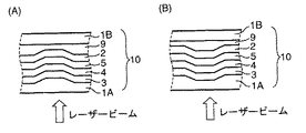
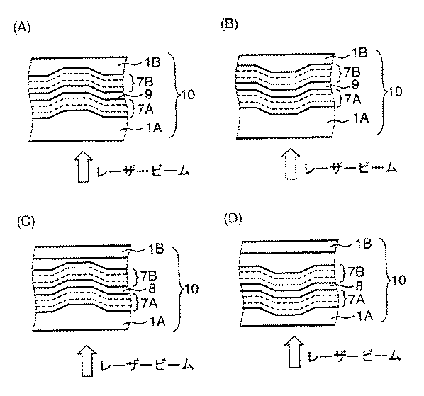
図1〜4は、本発明に係る光情報記録媒体(光ディスク)の実施形態を例示する断面模式図であり、波長が約350〜700nmのレーザ光を記録層に照射し、データの記録と再生を行うことのできる追記型の光ディスク示している。尚、各図の(A)[および(C)]は記録場所が凸状に形成されたもの、(B)[および(D)]は記録場所が凹状に形成されたものを例示している。 1 to 4 are cross-sectional schematic views illustrating an embodiment of an optical information recording medium (optical disk) according to the present invention. Data is recorded and reproduced by irradiating a recording layer with laser light having a wavelength of about 350 to 700 nm. 1 shows a write-once optical disc that can be used. In each figure, (A) [and (C)] are examples where the recording location is formed in a convex shape, and (B) [and (D)] are examples where the recording location is formed in a concave shape. .
図1の光ディスク10は、支持基板1と、光学調整層2と、誘電体層3,5と、該誘電体層3と5の間に挟まれた記録層4と、光透過層6とを備えている。誘電体層3,5は、記録層4を保護するために設けられたもので、これにより記録情報を長時間保存することができる。
1 includes a support substrate 1, an optical adjustment layer 2,
図2の光ディスク10は、支持基板1と、第0記録層群(光学調整層、誘電体層、記録層を備えた一群の層)7Aと、中間層8と、第1記録層群(光学調整層、誘電体層、記録層を備えた一群の層)7Bと、光透過層6とを備えている。図3は、1層DVD−R、1層DVD+R、1層HD DVD−Rタイプの光ディスクを例示し、図4は、2層DVD−R、2層DVD+R、2層HD DVD−Rタイプの光ディスクを例示するもので、符号8は中間層、符号9は接着剤層を示している。
2 includes a support substrate 1, a 0th recording layer group (a group of layers including an optical adjustment layer, a dielectric layer, and a recording layer) 7A, an
上記図2,4における第0および第1の記録層群7A,7Bを構成する一群の層は、3層構造(図の上側から、誘電体層/記録層/誘電体層、誘電体層/記録層/光学調整層、記録層/誘電体層/光学調整層など)や2層構造(図の上側から、記録層/誘電体層、誘電体層/記録層、記録層/光学調整層、光学調整層/記録層など)の他、記録層1層のみからなるものであっても構わない。
2 and 4, the group of layers constituting the 0th and first
なお本発明では、耐久性の評価基準を、「支持基板1に記録層4のみが形成されたサンプルを、温度80℃×相対湿度85%の環境下で96時間保持した前・後に、波長405nmの青色レーザ光を用いて測定した反射率の変化率が15%未満(好ましくは10%未満)を満足すること」としている。ちなみに、一般に青色レーザは波長が短く、膜劣化に対する反射率の変化が顕著であるため、青色レーザを用いて情報の記録や再生を行った光ディスクの耐久性は、赤色レーザを使用した場合よりも劣ることが予想される。そのため青色レーザ用の光記録層には、従来よりも高レベルの耐久性が求められるからである。
In the present invention, the evaluation criteria for durability is “wavelength 405 nm before and after holding a sample in which only the
こうした観点からすると、前掲の特許文献1,6でも光ディスクの耐久性を調べているが、その条件は、本発明よりも緩やかな環境条件である。ちなみに特許文献6では、本発明よりも耐久性試験温度が低く(温度60℃×相対湿度90%で120時間保持)、また特許文献1では、本発明よりも耐久性試験時間が短い(温度80℃×相対湿度85%で50時間保持)。即ちいずれの場合も、本発明の如く高温・高湿で長時間の耐久性試験は行っていない。
From this point of view, the above-mentioned
本発明の代表的な実施形態となる光ディスクは、例えば前記図1〜4に示した様な記録層4の素材として前掲の規定要件を満たすSn基合金を使用する点に特徴があり、記録層4以外の支持基板1や光学調整層2、誘電体層3,5などの素材は特に限定されず、通常使用されているものを適宜選択して使用できる。
The optical disk according to a typical embodiment of the present invention is characterized in that, for example, an Sn-based alloy that satisfies the above-mentioned prescribed requirements is used as a material of the
具体的には、支持基板の素材としては、ポリカーボネート樹脂、ノルボルネン系樹脂、環状オレフィン系共重合体、非晶質ポリオレフィンなど;光学調整層の素材としては、Ag,Au,Cu,Al,Ni,Cr,Ti等やそれらの合金など;誘電体層の素材としては、ZnS−SiO2,Si,Al,Ti,Ta,Zr,Crなどの酸化物、Ge,Cr,Si,Al,Nb,Mo,Ti,Znなどの窒化物、Ge,Cr,Si,Al,Ti,Zr,Taなどの炭化物、Si,Al,Mg,Ca,Laなどのフッ化物、或いはそれらの混合物などが例示される。 Specifically, the support substrate material is polycarbonate resin, norbornene resin, cyclic olefin copolymer, amorphous polyolefin, etc .; the optical adjustment layer material is Ag, Au, Cu, Al, Ni, Cr, Ti, etc. and alloys thereof; as a material for the dielectric layer, oxides such as ZnS—SiO 2 , Si, Al, Ti, Ta, Zr, Cr, Ge, Cr, Si, Al, Nb, Mo , Nitrides such as Ti, Zn, carbides such as Ge, Cr, Si, Al, Ti, Zr, Ta, fluorides such as Si, Al, Mg, Ca, La, or a mixture thereof.
なお、先にも述べた様に、光学調整層や誘電体層を形成すればディスクとしての反射率を高めることができるため、記録層の膜厚は1〜50nm、より好ましくは3〜30nm、更に好ましくは5〜20nmとするのがよい。 As described above, if the optical adjustment layer or the dielectric layer is formed, the reflectivity of the disk can be increased. Therefore, the recording layer has a thickness of 1 to 50 nm, more preferably 3 to 30 nm. More preferably, it is 5-20 nm.
また、本発明で規定する前記構成の光記録層を使用すれば、光学調整層2や誘電体層3,5の一部もしくは全部を省略することも可能である。光記録層単層の場合の好ましい膜厚は8〜50nm、より好ましくは10〜30nmである。
In addition, if the optical recording layer having the above-described configuration defined in the present invention is used, a part or all of the optical adjustment layer 2 and the
上記Sn基合金からなる光記録層は、スパッタリング法によって形成することが望ましい。即ち本発明で用いるSn以外の合金元素(Ni,Co,In,Bi,Zn,希土類元素)は、熱平衡状態ではSnに対し固有の固溶限を有しているが、スパッタリング法によって薄膜を形成すると、上記合金元素がSnマトリックス中に均一に分散するので、膜質が均質化し、安定した光学特性や耐環境性などが得られ易いからである。 The optical recording layer made of the Sn-based alloy is desirably formed by a sputtering method. That is, alloy elements (Ni, Co, In, Bi, Zn, and rare earth elements) other than Sn used in the present invention have a specific solid solubility limit with respect to Sn in a thermal equilibrium state, but a thin film is formed by sputtering. This is because the alloy elements are uniformly dispersed in the Sn matrix, so that the film quality is homogenized and stable optical characteristics and environmental resistance are easily obtained.
尚スパッタリングを行う際には、スパッタリング・ターゲット材として、溶解・鋳造法によって作製したSn基合金(以下、「溶製Sn基合金ターゲット材」という)を用いることが望ましい。溶製Sn基合金ターゲット材の組織は均一であり、スパッタ率が安定しているばかりでなく、ターゲットからの原子の出射角度も均一であるため、成分組成の均一な光記録層が得られ易く、均質で高性能の光ディスクを製造できるからである。 When sputtering is performed, it is desirable to use an Sn-based alloy (hereinafter referred to as “melted Sn-based alloy target material”) produced by a melting / casting method as a sputtering target material. The structure of the melted Sn-based alloy target material is uniform, the sputtering rate is stable, and the emission angle of atoms from the target is also uniform, so that an optical recording layer having a uniform composition can be easily obtained. This is because a homogeneous and high-performance optical disk can be manufactured.
なお、ターゲット材の製造に当っては、雰囲気中のガス成分(窒素、酸素など)や溶解炉成分が微量ながら不純物としてターゲット材に混入することがあるが、本発明の光記録層やターゲット材の成分組成は、それら不可避的に混入してくる微量成分までも規定するものではなく、本発明の上記特性が阻害されない限り、それら不可避不純物の微量の混入は許容される。 In the production of the target material, gas components (nitrogen, oxygen, etc.) and melting furnace components in the atmosphere may be mixed in the target material as impurities although they are in trace amounts. However, the optical recording layer or the target material of the present invention may be used. These component compositions do not stipulate even the trace components that are inevitably mixed in, and as long as the above characteristics of the present invention are not inhibited, the trace amounts of these unavoidable impurities are allowed.
以下、実施例を挙げて本発明をより具体的に説明するが、下記実施例はもとより本発明を制限する性質のものではなく、前・後記の趣旨を逸脱しない範囲で適宜変更を加えて実施することも可能であり、それらは本発明の技術的範囲に包含される。 Hereinafter, the present invention will be described more specifically with reference to examples. However, the following examples are not intended to limit the present invention as a matter of course, and are appropriately modified without departing from the spirit of the preceding and following descriptions. They are also possible and are within the scope of the present invention.
実施例1
本例は、Sn−Ni系合金(Sn−Ni合金、Sn−Ni−In合金、Sn−Ni−希土類元素合金、Sn−Ni−In−Y合金)およびSn−Co系合金(Sn−Co合金、Sn−Co−Bi合金)からなる光記録膜についての実施例である。なお、Sn−Ni−Co合金やSn−Ni−{Bi、Zn}合金からなる光記録膜についても同様の実験を行ったが、得られた結果に実質的な違いは認められなかった。
Example 1
In this example, Sn—Ni alloy (Sn—Ni alloy, Sn—Ni—In alloy, Sn—Ni—rare earth element alloy, Sn—Ni—In—Y alloy) and Sn—Co alloy (Sn—Co alloy) , Sn—Co—Bi alloy). A similar experiment was performed on an optical recording film made of a Sn—Ni—Co alloy or a Sn—Ni— {Bi, Zn} alloy, but no substantial difference was found in the obtained results.
1)ディスクの作製法
ディスク基板として、ポリカーボネート基板(厚さ:1.1mm、トラックピッチ:0.32μm、溝幅:0.14〜0.16μm、溝深さ:25nm)を用い、DCスパッタリング法によって光記録膜を成膜した。スパッタリング・ターゲットとしては、直径6インチのSnターゲット上に添加元素のチップを置いた複合ターゲットを用いた。
1) Disc production method A polycarbonate substrate (thickness: 1.1 mm, track pitch: 0.32 μm, groove width: 0.14 to 0.16 μm, groove depth: 25 nm) is used as a disk substrate, and a DC sputtering method is used. Then, an optical recording film was formed. As the sputtering target, a composite target in which a chip of an additive element was placed on a 6-inch diameter Sn target was used.
光記録膜形成のためのスパッタリング条件は、到達真空度:10−5Torr以下(1Torr=133.3Pa)、Arガス圧:4mTorr、DCスパッタパワー:100Wとした。なお記録膜の厚さは、スパッタリング時間を5〜120秒の間で変えることによって制御した。 The sputtering conditions for forming the optical recording film were as follows: ultimate vacuum: 10 −5 Torr or less (1 Torr = 133.3 Pa), Ar gas pressure: 4 mTorr, DC sputtering power: 100 W. The thickness of the recording film was controlled by changing the sputtering time between 5 and 120 seconds.
次いで、紫外線硬化型樹脂(日本化薬社製の商品名「BRD−130」)をスピンコートした後、紫外線硬化によって膜厚100±15μmの光透過層を形成した。 Subsequently, an ultraviolet curable resin (trade name “BRD-130” manufactured by Nippon Kayaku Co., Ltd.) was spin-coated, and then a light transmission layer having a thickness of 100 ± 15 μm was formed by ultraviolet curing.
2)光ディスクの評価法
光ディスク評価装置(パルステック社製の商品名「ODU−1000」、記録レーザ波長:405nm、NA(開口数):0.85)とスペクトラムアナライザー(アドバンテスト社製の商品名「R3131R」)を使用し、線速度5.28m/sにおいて、(1)未記録状態の周波数16.5MHzにおけるノイズレベル、(2)2T矩形波を各ディスクに記録したときの周波数16.5MHzにおけるC/N、(3)記録感度(C/Nが最大となる記録レーザ・パワー)、(4)ディスク状態での反射率(市販のBD−REディスクのSUM2レベル測定結果に基づき、SUM2レベル320mVを反射率16%と仮定して算出)を評価した。
2) Optical disk evaluation method Optical disk evaluation apparatus (trade name “ODU-1000” manufactured by Pulstec Corporation, recording laser wavelength: 405 nm, NA (numerical aperture): 0.85) and spectrum analyzer (trade name “manufactured by Advantest Corporation” R3131R ") at a linear velocity of 5.28 m / s, (1) noise level at an unrecorded frequency of 16.5 MHz, and (2) at a frequency of 16.5 MHz when a 2T rectangular wave is recorded on each disk. C / N, (3) recording sensitivity (recording laser power at which C / N is maximized), (4) reflectivity in disc state (based on SUM2 level measurement result of commercially available BD-RE disc, SUM2 level 320 mV Was calculated assuming that the reflectance was 16%.
結果を表1に纏めて示す。但し、表中の記号の意味は下記の通りである。
(1)未記録状態のノイズレベル
●:−75dB未満
◎:−75dB以上、−70dB未満
○:−70dB以上、−65dB未満
×:−65dB以上
(2)C/N
●:45dB超
◎:40dB以上、45dB未満
○:35dB以上、40dB未満
×:35dB未満
(3)記録感度
●:10mW未満
◎:10mW以上、15mW未満
○:15mW以上、20mW未満
×:20mW以上
(4)反射率
◎:15%以上、22%以下
○:10%以上、15%未満、または22%超、30%未満
×:10%未満または30%以上
The results are summarized in Table 1. However, the meanings of the symbols in the table are as follows.
(1) Noise level in an unrecorded state ●: Less than −75 dB ◎: −75 dB or more and less than −70 dB ○: −70 dB or more and less than −65 dB ×: −65 dB or more (2) C / N
●: More than 45 dB ◎: 40 dB or more, less than 45 dB ○: 35 dB or more, less than 40 dB ×: less than 35 dB (3) Recording sensitivity ●: Less than 10 mW ◎: 10 mW or more, less than 15 mW ○: 15 mW or more, less than 20 mW ×: 20 mW or more ( 4) Reflectance ◎: 15% or more, 22% or less ○: 10% or more, less than 15%, or more than 22%, less than 30% ×: Less than 10% or 30% or more
成膜した光記録膜の組成は、ICP発光分光法および質量分析法によって求めた。 The composition of the formed optical recording film was determined by ICP emission spectroscopy and mass spectrometry.
まず、Sn−Ni系合金(表1の試料No.1〜22、24〜28)について考察する。 First, Sn-Ni alloys (sample Nos. 1-22, 24-28 in Table 1) will be considered.
表1からも明らかな様に、Sn−Ni系合金中のNi含量が多くなるとノイズが低下し、C/Nが向上する。これは、Niの増量によって光記録膜の表面平滑性が向上することによるもので、Ni含量が15〜25原子%の範囲であるとき、全項目で優れた特性が得られている。 As is clear from Table 1, when the Ni content in the Sn—Ni alloy increases, noise decreases and C / N improves. This is because the surface smoothness of the optical recording film is improved by increasing the amount of Ni. When the Ni content is in the range of 15 to 25 atomic%, excellent characteristics are obtained in all items.
また、Sn−Ni系合金にInを添加すると、耐久性が更に向上し、記録特性(C/N、記録感度)とのバランス調整が可能である。なお、表1には、Inを含有する例しか示していないが、Inに替えてBiやZnを添加しても、In添加例とほぼ同様の傾向が見られることを実験により確認している。 Further, when In is added to the Sn—Ni-based alloy, durability is further improved, and balance adjustment with recording characteristics (C / N, recording sensitivity) is possible. In Table 1, only examples containing In are shown, but it has been confirmed by experiments that even if Bi or Zn is added instead of In, the same tendency as in the In addition examples is observed. .
また、Sn−Ni系合金に希土類元素を添加すると、表面平滑性や耐久性は更に向上する。殊に読み取り波形については、Sn−5原子%Ni―5原子%Nd合金膜よりも、Sn−5原子%Ni―5原子%Y合金膜の方がノイズ成分は少なかった。 Further, when a rare earth element is added to the Sn—Ni alloy, the surface smoothness and durability are further improved. In particular, regarding the read waveform, the Sn-5 atom% Ni-5 atom% Y alloy film had less noise component than the Sn-5 atom% Ni-5 atom% Nd alloy film.
総合的な評価として、本発明の規定要件を満たす光記録膜(試料No.1〜22)は、Snのみからなる光記録膜(試料No.23)やNiなどの含有量が本発明の規定要件を外れる光記録膜(試料No.24〜28)よりも優れた特性を有していることが分かる。 As a comprehensive evaluation, the optical recording films (samples Nos. 1 to 22) satisfying the prescribed requirements of the present invention have the contents of the optical recording film (sample No. 23) made of only Sn, Ni and the like defined by the present invention. It can be seen that the film has characteristics superior to those of optical recording films (samples Nos. 24-28) that deviate from the requirements.
上述したSn−Ni系合金と同様の傾向は、Sn−Co系合金からなる試料No.29〜31についても見られた。なお、表1には、Sn−Co系合金におけるCo含量を変えた例や希土類元素を更に添加した例などは示していないが、本発明で規定するCo含量を含むものや希土類元素を更に含むものは、全項目で優れた特性が得られることを実験によって確認している。また、Biの代わりにInやZnを用いても、上記と同様の効果が得られることを実験によって確認している。 A tendency similar to that of the above-described Sn—Ni-based alloy is the same as that of sample No. made of Sn—Co-based alloy. It was also seen for 29-31. Table 1 does not show an example in which the Co content in the Sn-Co alloy is changed or an example in which a rare earth element is further added. However, an alloy containing a Co content specified in the present invention or a rare earth element is further included. The thing has confirmed by experiment that the outstanding characteristic is acquired by all the items. Moreover, it has been confirmed by experiments that the same effect as described above can be obtained even if In or Zn is used instead of Bi.
実施例2
上記実施例1で作製したSn−15原子%Ni−3原子%Y合金よりなる光記録膜の上部(記録膜に引き続いて成膜;カバー層と記録層の間)や下部(基板上に成膜し、引き続き記録膜を成膜;基板と記録層の間)に直径4インチのZnS−SiO2ターゲットを用いて高周波スパッタリング法で誘電体膜を挿入したディスクを作製し、実施例1と同様にしてディスク評価を行った。スパッタリング条件は、到達真空度:10−5Torr以下、Arガス圧:2mTorr 、高周波スパッタパワー:200Wとした。なお膜厚は、スパッタリング時間を5〜120秒の間で変えることによって制御した。
Example 2
The upper part (deposited after the recording film; between the cover layer and the recording layer) or the lower part (formed on the substrate) of the Sn-15 atomic% Ni-3 atomic% Y alloy prepared in Example 1 above. Then, a recording film is formed; between the substrate and the recording layer) using a ZnS-SiO 2 target having a diameter of 4 inches, a disk in which a dielectric film is inserted by high frequency sputtering is prepared. The disk was evaluated. The sputtering conditions were: ultimate vacuum: 10 −5 Torr or less, Ar gas pressure: 2 mTorr, and high-frequency sputtering power: 200 W. The film thickness was controlled by changing the sputtering time between 5 and 120 seconds.
結果を表2に纏めて示す。なお、表2における記号の意味は表1と同じである。 The results are summarized in Table 2. The meanings of symbols in Table 2 are the same as those in Table 1.
表2からも明らかな様に、誘電体層を設けるとディスクでの反射率が増加することから、相対的に記録層の膜厚を薄くすることが可能となり、「ノイズ」、「C/N値」、「記録感度」のバランスが向上している。 As is clear from Table 2, since the reflectivity at the disc increases when the dielectric layer is provided, it is possible to relatively reduce the film thickness of the recording layer, and "noise", "C / N" The balance between “value” and “recording sensitivity” is improved.
実施例3
上記実施例1,2に示した試料について、光透過層のない光記録膜が露出した状態で、「温度80℃×相対湿度85%の環境下で96時間保持した前後に、波長405nmの青色レーザ光を用いて測定した反射率の変化率が15%未満(好ましくは10%未満)を満足する」という耐環境条件について試験を行なった。尚この試験では、日本分光社製の可視・紫外分光光度計「V−570」を用いて、分光絶対反射率を測定した。その結果、本発明の規定要件を満たす光記録膜は、全てこの耐環境条件を満たすことが確認された。
Example 3
For the samples shown in Examples 1 and 2, with the optical recording film having no light transmission layer exposed, “blue light having a wavelength of 405 nm before and after being held in an environment of temperature 80 ° C. × relative humidity 85% for 96 hours” The test was conducted on the environmental resistance condition that the reflectance change rate measured using laser light satisfies less than 15% (preferably less than 10%). In this test, a spectral absolute reflectance was measured using a visible / ultraviolet spectrophotometer “V-570” manufactured by JASCO Corporation. As a result, it was confirmed that all the optical recording films satisfying the prescribed requirements of the present invention satisfy this environmental resistance condition.
1 支持基板
2 光学調整層
3,5 誘電体層
4 記録層
6 光透過層
7A,7B 記録層群
8 中間層
9 接着剤層
10 光ディスク
DESCRIPTION OF SYMBOLS 1 Support substrate 2
Claims (10)
Priority Applications (1)
| Application Number | Priority Date | Filing Date | Title |
|---|---|---|---|
| JP2006352883A JP2007196683A (en) | 2005-12-27 | 2006-12-27 | Recording layer for optical information recording medium, optical information recording medium and sputtering target |
Applications Claiming Priority (2)
| Application Number | Priority Date | Filing Date | Title |
|---|---|---|---|
| JP2005376059 | 2005-12-27 | ||
| JP2006352883A JP2007196683A (en) | 2005-12-27 | 2006-12-27 | Recording layer for optical information recording medium, optical information recording medium and sputtering target |
Publications (1)
| Publication Number | Publication Date |
|---|---|
| JP2007196683A true JP2007196683A (en) | 2007-08-09 |
Family
ID=38451743
Family Applications (1)
| Application Number | Title | Priority Date | Filing Date |
|---|---|---|---|
| JP2006352883A Withdrawn JP2007196683A (en) | 2005-12-27 | 2006-12-27 | Recording layer for optical information recording medium, optical information recording medium and sputtering target |
Country Status (1)
| Country | Link |
|---|---|
| JP (1) | JP2007196683A (en) |
Cited By (3)
| Publication number | Priority date | Publication date | Assignee | Title |
|---|---|---|---|---|
| WO2011034188A1 (en) | 2009-09-18 | 2011-03-24 | 株式会社神戸製鋼所 | Recording layer for optical information recording medium, optical information recording medium, and sputtering target |
| WO2011034153A1 (en) | 2009-09-18 | 2011-03-24 | 株式会社神戸製鋼所 | Recording layer for optical information recording medium, optical information recording medium, and sputtering target |
| US8354155B2 (en) | 2008-11-12 | 2013-01-15 | Kobe Steel, Ltd. | Recording layer for optical information recording medium, optical information recording medium, and sputtering target |
-
2006
- 2006-12-27 JP JP2006352883A patent/JP2007196683A/en not_active Withdrawn
Cited By (5)
| Publication number | Priority date | Publication date | Assignee | Title |
|---|---|---|---|---|
| US8354155B2 (en) | 2008-11-12 | 2013-01-15 | Kobe Steel, Ltd. | Recording layer for optical information recording medium, optical information recording medium, and sputtering target |
| WO2011034188A1 (en) | 2009-09-18 | 2011-03-24 | 株式会社神戸製鋼所 | Recording layer for optical information recording medium, optical information recording medium, and sputtering target |
| WO2011034153A1 (en) | 2009-09-18 | 2011-03-24 | 株式会社神戸製鋼所 | Recording layer for optical information recording medium, optical information recording medium, and sputtering target |
| US8530024B2 (en) | 2009-09-18 | 2013-09-10 | Kobe Steel, Ltd. | Recording layer for optical information recording medium, optical information recording medium, and sputtering target |
| US8597757B2 (en) | 2009-09-18 | 2013-12-03 | Kobe Steel, Ltd. | Recording layer for optical information recording medium, optical information recording medium, and sputtering target |
Similar Documents
| Publication | Publication Date | Title |
|---|---|---|
| KR100445083B1 (en) | Reflection layer or semi-transparent reflection layer for use in optical information recording medium, optical information recording medium and sputtering target for use in the optical information recording medium | |
| KR100720203B1 (en) | Silver alloy reflective film, sputtering target therefor, and optical information recording medium using the same | |
| US7790263B2 (en) | Ag alloy reflective film for optical information recording medium, optical information recording medium and Ag alloy sputtering target for forming Ag alloy reflective film for optical information recording medium | |
| JP4377861B2 (en) | Ag alloy reflecting film for optical information recording medium, optical information recording medium, and Ag alloy sputtering target for forming Ag alloy reflecting film for optical information recording medium | |
| KR20060033047A (en) | Optical record carrier, manufacturing method thereof, method of recording data on optical record carrier and data reproduction method | |
| US20070048488A1 (en) | Recording layer and sputtering target for optical information recording media, as well as optical information recording media | |
| US20090046566A1 (en) | Recording layer for optical information recording medium, optical information recording medium, and sputtering target for optical information recording medium | |
| KR100770806B1 (en) | Optical recording medium, method for producing the same, and data recording method and data reproducing method for optical recording medium | |
| JP2007230207A (en) | Recording layer for optical information recording medium, optical information recording medium, and spattering target | |
| JP2009076129A (en) | Read-only optical information recording medium | |
| JP2007196683A (en) | Recording layer for optical information recording medium, optical information recording medium and sputtering target | |
| US20070248783A1 (en) | Optical information recording media | |
| JP4540687B2 (en) | Read-only optical information recording medium | |
| JP4110194B1 (en) | Optical information recording medium | |
| JP2007301761A (en) | Recording layer for optical information recording medium and optical information recording medium | |
| JP2008302688A (en) | Optical information recording medium | |
| JP2007111898A (en) | Recording layer and sputtering target for optical information recording medium, and optical information recording medium | |
| JP2007196571A (en) | Recording layer for optical information recording medium, optical information recording medium and sputtering target | |
| JP2007185810A (en) | Optical information recording medium and sputtering target for forming recording layer of optical information recording medium | |
| JP2009090601A (en) | Recording layer for optical information recording medium, optical information recording medium, and sputtering target | |
| JP2007334983A (en) | Optical information recording medium | |
| JP2009233952A (en) | Optical information recording medium | |
| JP2007118463A (en) | Recording layer and spattering target for optical information recording medium, and optical information recording medium | |
| JP2009143184A (en) | Recording layer for optical information recording medium and optical information recording medium | |
| JP2009301623A (en) | Write-once type optical recording medium |
Legal Events
| Date | Code | Title | Description |
|---|---|---|---|
| A300 | Application deemed to be withdrawn because no request for examination was validly filed |
Free format text: JAPANESE INTERMEDIATE CODE: A300 Effective date: 20100302 |