JP2007196621A - Signal processing device and imaging device - Google Patents
Signal processing device and imaging device Download PDFInfo
- Publication number
- JP2007196621A JP2007196621A JP2006020680A JP2006020680A JP2007196621A JP 2007196621 A JP2007196621 A JP 2007196621A JP 2006020680 A JP2006020680 A JP 2006020680A JP 2006020680 A JP2006020680 A JP 2006020680A JP 2007196621 A JP2007196621 A JP 2007196621A
- Authority
- JP
- Japan
- Prior art keywords
- image
- correction
- signal
- unit
- control unit
- Prior art date
- Legal status (The legal status is an assumption and is not a legal conclusion. Google has not performed a legal analysis and makes no representation as to the accuracy of the status listed.)
- Pending
Links
- 238000012545 processing Methods 0.000 title claims abstract description 71
- 238000003384 imaging method Methods 0.000 title description 11
- 238000012937 correction Methods 0.000 claims abstract description 213
- 238000012546 transfer Methods 0.000 claims abstract description 77
- 238000001514 detection method Methods 0.000 claims abstract description 56
- 230000003287 optical effect Effects 0.000 claims abstract description 55
- 238000004458 analytical method Methods 0.000 claims abstract description 38
- 238000006243 chemical reaction Methods 0.000 claims abstract description 12
- 239000000284 extract Substances 0.000 claims abstract description 5
- 239000000428 dust Substances 0.000 claims description 15
- 230000015572 biosynthetic process Effects 0.000 claims description 10
- 230000008859 change Effects 0.000 abstract description 5
- 239000000470 constituent Substances 0.000 abstract 1
- 238000000034 method Methods 0.000 description 35
- 230000008569 process Effects 0.000 description 30
- 238000005070 sampling Methods 0.000 description 28
- 238000005259 measurement Methods 0.000 description 25
- 238000004140 cleaning Methods 0.000 description 9
- 101000860173 Myxococcus xanthus C-factor Proteins 0.000 description 7
- 239000003086 colorant Substances 0.000 description 7
- 239000004065 semiconductor Substances 0.000 description 5
- 238000004891 communication Methods 0.000 description 4
- 230000007246 mechanism Effects 0.000 description 4
- 238000010586 diagram Methods 0.000 description 3
- 230000006870 function Effects 0.000 description 3
- 239000000758 substrate Substances 0.000 description 3
- 238000011161 development Methods 0.000 description 2
- 230000002093 peripheral effect Effects 0.000 description 2
- 230000004044 response Effects 0.000 description 2
- 230000001960 triggered effect Effects 0.000 description 2
- 238000003705 background correction Methods 0.000 description 1
- 230000006835 compression Effects 0.000 description 1
- 238000007906 compression Methods 0.000 description 1
- 238000012217 deletion Methods 0.000 description 1
- 230000037430 deletion Effects 0.000 description 1
- 238000013461 design Methods 0.000 description 1
- 238000000605 extraction Methods 0.000 description 1
- 230000005484 gravity Effects 0.000 description 1
- 239000004973 liquid crystal related substance Substances 0.000 description 1
- 230000000873 masking effect Effects 0.000 description 1
- 208000028780 ocular motility disease Diseases 0.000 description 1
- 108091008695 photoreceptors Proteins 0.000 description 1
- 238000011144 upstream manufacturing Methods 0.000 description 1
Images


Classifications
-
- G—PHYSICS
- G03—PHOTOGRAPHY; CINEMATOGRAPHY; ANALOGOUS TECHNIQUES USING WAVES OTHER THAN OPTICAL WAVES; ELECTROGRAPHY; HOLOGRAPHY
- G03G—ELECTROGRAPHY; ELECTROPHOTOGRAPHY; MAGNETOGRAPHY
- G03G15/00—Apparatus for electrographic processes using a charge pattern
- G03G15/01—Apparatus for electrographic processes using a charge pattern for producing multicoloured copies
- G03G15/0105—Details of unit
- G03G15/0131—Details of unit for transferring a pattern to a second base
-
- G—PHYSICS
- G03—PHOTOGRAPHY; CINEMATOGRAPHY; ANALOGOUS TECHNIQUES USING WAVES OTHER THAN OPTICAL WAVES; ELECTROGRAPHY; HOLOGRAPHY
- G03G—ELECTROGRAPHY; ELECTROPHOTOGRAPHY; MAGNETOGRAPHY
- G03G2215/00—Apparatus for electrophotographic processes
- G03G2215/01—Apparatus for electrophotographic processes for producing multicoloured copies
- G03G2215/0151—Apparatus for electrophotographic processes for producing multicoloured copies characterised by the technical problem
- G03G2215/0158—Colour registration
- G03G2215/0161—Generation of registration marks
Landscapes
- Physics & Mathematics (AREA)
- General Physics & Mathematics (AREA)
- Control Or Security For Electrophotography (AREA)
- Color Electrophotography (AREA)
- Facsimile Image Signal Circuits (AREA)
- Laser Beam Printer (AREA)
- Electrostatic Charge, Transfer And Separation In Electrography (AREA)
Abstract
Description
本発明は、信号処理装置及び画像形成装置に関する。 The present invention relates to a signal processing apparatus and an image forming apparatus.
従来、カラーの電子写真方式の複写機等の画像形成装置において、Y(イエロー)、M(マゼンダ)、C(シアン)、K(黒)のトナー像の重ね合せにより画像形成されている。各色のトナー像が各色の感光体ドラム上に現像され、中間転写体としての環状のベルト上に各色のトナー像が順に重ねて転写され、その転写像が記録用紙に転写される。 Conventionally, in an image forming apparatus such as a color electrophotographic copying machine, an image is formed by superimposing toner images of Y (yellow), M (magenta), C (cyan), and K (black). The toner images of the respective colors are developed on the photosensitive drums of the respective colors, the toner images of the respective colors are sequentially transferred onto an annular belt as an intermediate transfer member, and the transferred image is transferred onto a recording sheet.
中間転写体上に所定の濃度パッチ、レジストマーク(パターン)を形成して、その画像を光学式センサで検知し、その検知信号に基づいて、濃度補正、カラーレジスト補正を行う構成が実施されている。カラーレジスト補正は、各色のレジストマークの位置をセンサで検出して、そのずれ量に基づいて、主走査補正量、副走査補正量、全体横倍補正量、部分横倍補正量、スキュー補正量(走査線の傾き補正量)を算出して色ずれを補正する。 A configuration has been implemented in which predetermined density patches and registration marks (patterns) are formed on the intermediate transfer member, the image is detected by an optical sensor, and density correction and color resist correction are performed based on the detection signal. Yes. In color registration correction, the position of each color registration mark is detected by a sensor, and based on the amount of deviation, main scanning correction amount, sub-scanning correction amount, overall horizontal magnification correction amount, partial horizontal magnification correction amount, skew correction amount The (scan line inclination correction amount) is calculated to correct the color misregistration.
カラーレジスト補正において、センサからの検知信号を2値化し、その2値化データに対して、中間転写体上へのレジストマークの書き出しタイミングからその位置を推定し、推定範囲+αの範囲でそのレジストマークの検出を行い、その範囲以外をシーケンス的にマスクすることにより、中間転写体上の傷、ごみによるノイズ除去を行う方法が考えられている(例えば、特許文献1参照)。 In color registration correction, the detection signal from the sensor is binarized, and the position of the binarized data is estimated from the registration mark writing timing on the intermediate transfer member, and the registration signal is within the estimated range + α. A method is considered in which noise is detected by scratches and dust on the intermediate transfer member by detecting marks and sequentially masking areas other than the range (see, for example, Patent Document 1).
また、カラーレジスト補正において、センサからの検知信号に対して、IIR(infinite Impulse Response)型、FIR(infinite Impulse Response)型、移動平均型のデジタルローパスフィルタをかけて、中間転写体上の傷、ごみによるノイズ除去を行う方法も考えられている(例えば、特許文献2参照)。
しかし、従来の所定範囲のレジストマーク検出によるノイズ除去方法では、その所定範囲の信号を信頼し、そこに発生したノイズ成分を含めてレジストマーク検出を行うので、初期時には問題なくても、経時的な変化等により、管理できない要因となっていた。 However, in the conventional noise removal method by detecting the registration mark within a predetermined range, since the signal within the predetermined range is trusted and the registration mark is detected including the noise component generated there, even if there is no problem at the initial stage, It was a factor that could not be managed due to various changes.
また、従来のローパスフィルタによるノイズ除去方法では、簡単な構成で実施しようとすると、レジストマーク検出が正確に得られなくなるおそれがあった。 Further, in the conventional noise removal method using a low-pass filter, there is a possibility that registration mark detection cannot be obtained accurately if an attempt is made with a simple configuration.
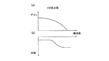
図14(a)に、低次数のFIRフィルタにおける周波数に対するゲインを示す。図14(b)に、低次数のFIRフィルタにおける周波数に対する位相成分を示す。図15(a)に、高次数のFIRフィルタにおける周波数に対するゲインを示す。図15(b)に、高次数のFIRフィルタにおける周波数に対する位相成分を示す。図14(a),(b)に示すように、FIRフィルタを低次数で実現すると、フィルタ特性になまりが生じるという問題があった。また、図15(a),(b)に示すように、FIRフィルタを高次数で実現すると、フィルタ特性は安定するが、次数に応じた遅れが波形に生じ、位置検知の精度に影響が出るという問題があった。 FIG. 14A shows the gain with respect to the frequency in the low-order FIR filter. FIG. 14B shows phase components with respect to frequency in the low-order FIR filter. FIG. 15A shows the gain with respect to the frequency in the high-order FIR filter. FIG. 15B shows phase components with respect to frequency in the high-order FIR filter. As shown in FIGS. 14A and 14B, when the FIR filter is realized with a low order, there is a problem that the filter characteristics are distorted. As shown in FIGS. 15A and 15B, when the FIR filter is realized with a high order, the filter characteristics are stabilized, but a delay corresponding to the order is generated in the waveform, which affects the position detection accuracy. There was a problem.
また、IIRフィルタは、帰還を行うことでフィルタ特性を良好にするものであるが、設計次第では安定性に欠ける系となってしまい、対象の経時的変化等を十分に把握し設計しなければならないという問題があった。 The IIR filter improves the filter characteristics by performing feedback. However, depending on the design, the IIR filter becomes a system that lacks stability. There was a problem of not becoming.
本発明の課題は、経時変化によらずに、補正用画像の検知信号からノイズ成分を高精度に削除することである。 An object of the present invention is to delete a noise component from a detection signal of a correction image with high accuracy regardless of a change with time.
上記の課題を解決するために、請求項1に記載の発明の信号処理装置は、
補正用画像の形成対象の記録媒体の表面を検知して検知信号を出力する光学式センサと、
前記補正用画像が形成されていない前記記録媒体の表面を前記光学式センサに検知させ、当該光学式センサから出力される検知信号に周波数解析を行い、その第1の解析信号から他の値よりも卓越した周波数成分に対応する卓越周波数を抽出し、前記補正用画像が形成された前記記録媒体の表面を前記光学式センサに検知させ、当該光学式センサから出力される検知信号に周波数解析を行い、その第2の解析信号から前記卓越周波数の成分を削除し、当該卓越周波数成分を削除した解析信号に逆周波数変換を行い当該卓越周波数成分を削除した検知信号を算出する制御手段と、を備えることを特徴とする。
In order to solve the above-described problem, a signal processing apparatus according to
An optical sensor that detects the surface of the recording medium on which a correction image is to be formed and outputs a detection signal;
The optical sensor detects the surface of the recording medium on which the image for correction is not formed, performs frequency analysis on the detection signal output from the optical sensor, and determines other values from the first analysis signal. Also extracts the dominant frequency corresponding to the outstanding frequency component, causes the optical sensor to detect the surface of the recording medium on which the correction image is formed, and performs frequency analysis on the detection signal output from the optical sensor. And a control means for deleting the dominant frequency component from the second analysis signal, performing inverse frequency conversion on the analysis signal from which the dominant frequency component has been deleted, and calculating a detection signal from which the dominant frequency component has been deleted. It is characterized by providing.
請求項2に記載の発明は、請求項1に記載の信号処理装置において、
前記制御手段は、前記第1の解析信号において、前記記録媒体の表面の傷又はごみに起因するノイズが発生する周波数範囲から卓越周波数を抽出することを特徴とする。
The invention according to
The control means extracts a dominant frequency from a frequency range in which noise is generated due to scratches or dust on the surface of the recording medium in the first analysis signal.
請求項3に記載の発明は、請求項1又は2に記載の信号処理装置において、
前記補正用画像は、画像形成の濃度補正用の濃度パッチを含み、
前記制御手段は、前記濃度パッチの検知により算出される前記卓越周波数成分を削除した検知信号に基づいて、濃度情報を算出することを特徴とする。
The invention according to claim 3 is the signal processing apparatus according to
The correction image includes a density patch for density correction for image formation,
The control means calculates density information based on a detection signal from which the dominant frequency component calculated by detecting the density patch is deleted.
請求項4に記載の発明は、請求項1から3のいずれか一項に記載の信号処理装置において、
前記補正用画像は、画像形成のレジスト補正用のレジストマークを含み、
前記制御手段は、前記レジストマークの検知により算出される前記卓越周波数成分を削除した検知信号に基づいて、前記レジストマークの位置情報を算出することを特徴とする。
The invention according to
The correction image includes a registration mark for image formation registration correction,
The control means calculates position information of the registration mark based on a detection signal from which the dominant frequency component calculated by detection of the registration mark is deleted.
請求項5に記載の発明は、請求項1から4のいずれか一項に記載の信号処理装置において、
前記制御手段は、前記卓越周波数成分を削除した検知信号に基づいて、画像形成に関する補正を行うための補正情報を算出することを特徴とする。
The invention according to
The control means calculates correction information for performing correction related to image formation based on a detection signal from which the dominant frequency component is deleted.
請求項6に記載の発明は、請求項1から5のいずれか一項に記載の信号処理装置において、
前記記録媒体は、中間転写体であることを特徴とする。
The invention according to claim 6 is the signal processing device according to any one of
The recording medium is an intermediate transfer member.
請求項7に記載の発明の画像形成装置は、
請求項1から6のいずれか一項に記載の信号処理装置と、
前記記録媒体に画像形成する画像形成手段と、を備え、
前記補正用画像は、前記画像形成手段により画像形成されることを特徴とする。
According to a seventh aspect of the present invention, there is provided an image forming apparatus.
A signal processing device according to any one of
Image forming means for forming an image on the recording medium,
The correction image is formed by the image forming unit.
本発明によれば、経時変化によらずに、補正用画像の検知信号からノイズ成分を高精度に削除できる。 According to the present invention, it is possible to delete a noise component from a detection signal of a correction image with high accuracy regardless of a change with time.
以下、図面を参照して本発明に係る実施の形態を詳細に説明する。ただし、発明の範囲は、図示例に限定されない。 Hereinafter, embodiments of the present invention will be described in detail with reference to the drawings. However, the scope of the invention is not limited to the illustrated examples.
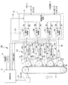
先ず、図1〜図5を参照して、本実施の形態のカラー画像形成装置(カラー複写機)100の装置構成を説明する。図1に、カラー画像形成装置100の印刷処理に関する構成を示す。
First, an apparatus configuration of a color image forming apparatus (color copying machine) 100 according to the present embodiment will be described with reference to FIGS. FIG. 1 shows a configuration relating to printing processing of the color
図1に示すように、カラー画像形成装置100は、画像形成装置本体101と、画像形成装置本体101の上部の画像読取装置102と、を備える。画像読取装置102は、自動原稿給紙装置201と、原稿画像走査露光装置202と、を備える。
As shown in FIG. 1, the color
自動原稿給紙装置201の原稿台に載置された原稿dは搬送手段により搬送され、原稿画像走査露光装置202の光学系により原稿の片面又は両面の画像が走査露光され、原稿画像を反映する入射光がラインイメージセンサCCDに読み込まれる。
The document d placed on the document table of the
上記ラインイメージセンサCCDにより光電変換されたアナログ画像信号は、画像処理手段70(図3参照)において、アナログ処理、A/D変換、シェーディング補正及び画像圧縮処理等が施され、デジタルの画像データとなる。このデジタルの画像データは、画像書き込みユニット3Y,3M,3C,3Kへ入力される。
The analog image signal photoelectrically converted by the line image sensor CCD is subjected to analog processing, A / D conversion, shading correction, image compression processing, and the like in an image processing means 70 (see FIG. 3). Become. This digital image data is input to the
自動原稿給紙装置201は、自動両面原稿搬送手段(図示略)を備える。自動原稿給紙装置201は、原稿載置台から搬送される多数枚の原稿dの内容(片面又は両面)を連続して一挙に読み取り、原稿内容を画像メモリ50(図5参照)に蓄積する(電子RDH機能)。この電子RDH機能は、複写機能により多数枚の原稿内容を複写する場合、或いはファクシミリ機能により多数枚の原稿dを送信する場合等に利用される。
The
画像形成装置本体101は、複数の感光体ドラム1Y,1M,1C,1Kが縦列に配置されたタンデム型のカラー画像形成装置であり、画像形成ユニット10Y,10M,10C,10Kを有する画像形成手段103を備える。感光体ドラム1Y,1M,1C,1Kの各々は、それぞれ順に、画像形成ユニット10Y,10M,10C,10Kに設けられている。以下、各部の符号のY、M、C、Kは、それぞれ順に、イエロー色、マゼンタ色、シアン色、黒色を表すものとする。
The image forming apparatus
更に、画像形成装置本体101は、中間転写体6と、再給紙機構(ADU機構)を含む給紙搬送手段(図示略)と、トナー像を定着させるための定着装置17と、を備える。
Further, the image forming apparatus
Y色の画像を形成する画像形成ユニット10Yは、Y色のトナー像が形成される感光体ドラム1Yと、感光体ドラム1Yの周囲に配置された、感光体ドラム1Y表面を帯電するY色用の帯電手段2Yと、その帯電面に画像パターンを露光して静電潜像を形成する画像書き込みユニット3Yと、その潜像面をY色のトナーで現像しトナー像を形成する現像装置4Yと、中間転写体6へのトナー像の転写後にトナーを除去する感光体ドラム用クリーニング手段8Yと、を有する。
The
M色の画像を形成する画像形成ユニット10Mは、同様に、M色のトナー像が形成される感光体ドラム1Mと、感光体ドラム1Mの周囲に配置されたM色用の帯電手段2M、画像書き込みユニット3M、現像装置4M及び感光体ドラム用クリーニング手段8Mを有する。
Similarly, the
C色の画像を形成する画像形成ユニット10Cは、同様に、C色のトナー像が形成される感光体ドラム1Cと、感光体ドラム1Cの周囲に配置されたC色用の帯電手段2C、画像書き込みユニット3C、現像装置4C及び感光体ドラム用クリーニング手段8Cを有する。
Similarly, an
K色の画像を形成する画像形成ユニット10Kは、同様に、K色のトナー像が形成される感光体ドラム1K、感光体ドラム1Kの周囲に配置されたK色用の帯電手段2K、画像書き込みユニット3K、現像装置4K及び感光体ドラム用クリーニング手段8Kを有する。
Similarly, the
帯電手段2Y及び画像書き込みユニット3Yと、帯電手段2M及び画像書き込みユニット3Mと、帯電手段2C及び画像書き込みユニット3Cと、帯電手段2K及び画像書き込みユニット3Kとは、それぞれ、感光体ドラム1Y,1M,1C,1Kに色毎の静電潜像を形成する。
The charging
画像書き込みユニット3Y,3M,3C,3Kの各々は、後述する制御手段15から出力されるスキュー調整信号SSy,SSm、SScの各々に基づいてスキュー補正(画像の傾き調整)を行う。また、画像書き込みユニット3Y,3M,3C,3Kの各々は、制御手段15から出力されるY色用の書き込みデータWy、M色用の書き込みデータWm、C色用の書き込みデータWc、K色用の書き込みデータWkの各々に基づいて、感光体ドラム1Y,1M,1C,1Kに露光し、Y色、M色、C色、K色のトナー画像を中間転写体6に形成する。
Each of the
現像装置4Y,4M,4C,4Kによる現像は、使用するトナー極性と同極性(本実施の形態においては、負極性)の直流電圧に交流電圧を重畳した現像バイアスを用いた反転現像に基づくものである。
Development by the developing
中間転写体6は、環状のベルト部が回転動作可能に保持され、感光体ドラム1Y,1M,1C,1Kの各々に形成されたY色、M色、C色、K色の各トナー像は中間転写体6の当該ベルト部表面に転写される。
The intermediate transfer member 6 has an annular belt portion that is rotatably supported, and Y, M, C, and K toner images formed on the
中間転写体用クリーニング手段8Aの上流側であって、中間転写体6の左右両側には、1対の光学式センサ12A,12Bが設けられている。図2に、補正用画像が形成された中間転写体6及び光学式センサ12A,12Bの構成を示す。
A pair of
光学式センサ12A,12Bは、CCD(Charge-Coupled Devices)センサや、LED(Laser Emitting Diode)等の発光素子及びPD(Photo Diode)等の受光素子の組み合わせによる反射型のフォトセンサ等である(何れも図示略)。図2に示すように、光学式センサ12A,12Bは、後述するベースライン測定の際に、トナー像が形成されていない中間転写体6の表面状態を光学的に検知し、後述するレジスト補正、階調補正の際に、画像形成ユニット10Y,10M,10C,10Kにより、レジストレーション補正用の基準色(本実施の形態においては、K色とする)を含む各色の画像(以下、レジストマークCRとする)と、濃度補正としての階調補正用の画像(以下、濃度パッチPTとする)と、が形成された中間転写体6の表面状態を光学的に検知し、光電変換してアナログの電気信号を制御手段15(信号処理部153)に出力する。
The
ここで、上記したカラー画像形成装置100による画像形成プロセスの概要について述べる。画像形成ユニット10Y,10M,10C,10Kにより形成された各色の画像は、使用するトナーと反対極性(本実施の形態においては、正極性)の1次転写バイアスが印加される1次転写ローラ7Y,7M,7C,7Kにより、回転動作する中間転写体6のベルト表面に逐次転写されて(1次転写)、合成されたカラー画像(色画像:カラートナー像)が形成される。カラー画像は中間転写体6から印刷用紙Pへ転写される。
Here, an outline of the image forming process by the color
給紙カセット20A,20B,20C内に収容された印刷用紙Pは、給紙カセット20A,20B,20Cにそれぞれ設けられている送り出しローラ21及び給紙ローラ22Aにより給紙され、搬送ローラ22B,22C,22D、レジストローラ23等を経て、2次転写ローラ7Aに搬送され、印刷用紙Pの一方の面(表面又は裏面)にカラー画像が転写される(2次転写)。
The printing paper P accommodated in the
カラー画像が転写された印刷用紙Pは、定着装置17により定着処理され、排紙ローラ24により挟持されて機外の排紙トレイ25に載置される。転写後の感光体ドラム1Y,1M,1C,1Kの周面上に残る転写残トナーは、感光体ドラム用クリーニング手段8Y,8M,8C,8Kによりクリーニングされ次の画像形成サイクルに移行する。
The printing paper P to which the color image has been transferred is subjected to fixing processing by the fixing
両面画像形成時には、印刷用紙Pの一方の面(表面)に画像形成され、定着装置17から排出された印刷用紙Pは、分岐手段26によりシート排紙路から分岐され、下方の循環通紙路27Aを経て、再給紙機構(ADU機構)である反転搬送路27Bにより表裏が反転され、再給紙搬送部27Cを通過して、搬送ローラ22Dにおいて合流する。
At the time of double-sided image formation, the printing paper P formed on one surface (front surface) of the printing paper P and discharged from the fixing
反転搬送された印刷用紙Pは、レジストローラ23を経て再度2次転写ローラ7Aに搬送され、印刷用紙Pの他方の面(裏面)にカラー画像(カラートナー像)が転写される。カラー画像が転写された印刷用紙Pは、定着装置17により定着処理され、排紙ローラ24に挟持されて機外の排紙トレイ25に載置される。一方、2次転写ローラ7Aにより印刷用紙Pにカラー画像が転写された後、印刷用紙Pが分離された中間転写体6は、中間転写体用クリーニング手段8Aにより残留トナーが除去される。
The reversely conveyed printing paper P is conveyed again to the
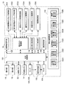
次に、図3及び図4を参照してカラー画像形成装置100のデータ処理に係る機能構成について説明する。図3に、カラー画像形成装置100のデータ処理に係る機能構成を示す。
Next, a functional configuration related to data processing of the color
図3に示すように、カラー画像形成装置100は、上述した図1に示す印刷処理に係る各構成部の他に、補正手段5Y,5M,5C、光学式センサ12A,12B、不揮発メモリ14、制御手段15、レーザインデックスセンサ49、画像処理手段70等を備える。
As shown in FIG. 3, the color
補正手段5Y,5M,5Cは、制御手段15から出力された位置補正信号Sy,Sm,Scに応じて、画像書き込みユニット3Y,3M,3Cの水平方向の傾きをそれぞれ調整する。
The correction means 5Y, 5M, and 5C adjust the horizontal inclinations of the
不揮発メモリ14は、制御手段15により実行される各種プログラム実行時に生成される各種データを格納する。また、不揮発メモリ14は、予め、レジスト補正量(レジスト補正用LUT)、階調補正量(階調補正用LUT)、倍率補正用LUT、補正用画像データを記憶するものとする。
The
制御手段15は、プログラム又はハードウェアによってカラー画像形成装置100を統括的に制御する。
The
制御手段15は、画像形成ユニット10Y,10M,10C,10Kを制御して、画像処理手段70から出力されるY色用の書き込みデータWy、M色用の書き込みデータWm、C色用の書き込みデータWc、K色用の書き込みデータWkに基づき、Y色、M色、C色、K色のトナー画像を中間転写体6に形成させる。
The
制御手段15は、画像処理制御信号S4を画像処理回路71に出力して、画像処理回路71の動作を制御する。 The control means 15 outputs an image processing control signal S4 to the image processing circuit 71 and controls the operation of the image processing circuit 71.
制御手段15は、書込選択信号S5を、Y−信号切換部72Y、M−信号切換部72M、C−信号切換部72C、K−信号切換部72Kの各々に出力して制御する。
The control means 15 outputs and controls the write selection signal S5 to each of the Y-
制御手段15は、位置補正信号Sy,Sm,Scの各々を補正手段5Y,5M,5Cにそれぞれ出力し、画像書き込みユニット3Y,3M,3Cの各水平方向の傾きをそれぞれ調整させる。
The control means 15 outputs the position correction signals Sy, Sm and Sc to the correction means 5Y, 5M and 5C, respectively, and adjusts the horizontal inclinations of the
制御手段15は、スキュー調整信号SSy,SSm,SScの各々を画像書き込みユニット3Y,3M,3Cにそれぞれ出力し、画像書き込みユニット3Y,3M,3Cのスキュー調整を行う。
The
制御手段15は、レーザインデックスセンサ49から入力される各色毎のINDEX信号に基づいて、印刷用データの出力開始タイミングを生成する。
Based on the INDEX signal for each color input from the
ここで、出力開始タイミングとは、Y−信号切換部72Y、M−信号切換部72M、C−信号切換部72C、K−信号切換部72Kが、それぞれ、画像書き込みユニット3Y,3M,3C,3Kの各々に書き込みデータWy,Wm,Wc,Wkを出力する際のタイミングである。
Here, the output start timing means that the Y-
制御手段15は、印刷倍率(例えば、両面印刷時の裏面に対する印刷倍率)の変更指示が後述する操作部16を介して入力されると、当該変更された印刷倍率と倍率補正用LUT(Look Up Table)とに基づいてプロセス速度又はポリゴンミラー34の回転速度を設定して当該変更された印刷倍率に基づいた印刷を行う。
When an instruction to change the printing magnification (for example, the printing magnification for the back side during double-sided printing) is input via the
ここで倍率補正用LUTとは、印刷倍率と、プロセス速度又はポリゴンミラー34の回転速度との対応関係を示すデータであり、不揮発メモリ14に予め格納されている。
Here, the magnification correction LUT is data indicating a correspondence relationship between the printing magnification and the process speed or the rotation speed of the
制御手段15は、ベースライン測定処理及び補正用画像測定処理(図6、図9のフローチャートに示す処理)を行うよう制御する。
The
レーザインデックスセンサ49は、画像書き込みユニット3Y,3M,3C,3Kの各々から照射されるビーム光を検知して、INDEX信号を制御手段15に出力する。
The
画像処理手段70は、画像処理回路71、Y−信号切換部72Y、M−信号切換部72M、C−信号切換部72C、K−信号切換部72Kを備える。
The image processing means 70 includes an image processing circuit 71, a Y-
画像処理回路71は、画像処理制御信号S4に基づき、画像読取装置102により読み取られたカラー画像のR、G、B色成分に係るR、G、B信号を色変換し、画像データDy,Dm,Dc,Dkの各々を、Y−信号切換部72Y、M−信号切換部72M、C−信号切換部72C、K−信号切換部72Kに出力する。
Based on the image processing control signal S4, the image processing circuit 71 performs color conversion on the R, G, and B signals related to the R, G, and B color components of the color image read by the
画像処理回路71は、プリンタ等の外部機器から入力されるY、M、C、K信号に対しては、画像処理制御信号S4に基づいて各信号をスクリーン処理した後の画像データDy',Dm',Dc',Dk'のそれぞれを、Y−信号切換部72Y、M−信号切換部72M、C−信号切換部72C、K−信号切換部72Kに出力する。
For the Y, M, C, and K signals input from an external device such as a printer, the image processing circuit 71 performs image processing on each signal based on the image processing control signal S4 and outputs image data Dy ′ and Dm. ', Dc' and Dk 'are output to the Y-
Y−信号切換部72Y、M−信号切換部72M、C−信号切換部72C、K−信号切換部72Kは、それぞれ、書込選択信号S5に基づき、画像データDy又は画像データDy'の何れか一方、画像データDm又は画像データDm'の何れか一方、画像データDc又は画像データDc'の何れか一方、画像データDk又は画像データDk'の何れか一方を各々選択して画像書き込みユニット3Y,3M,3C,3Kに出力する。
The Y-
次に、図4を参照して、画像書き込みユニット3Yの構成について説明する。図4に、画像書き込みユニット3Yの構成を示す。なお、ここでの説明は、Y色以外の他の色(M色、C色、K色)用の画像書き込みユニット3M,3C,3K等に対しても全く同様である。
Next, the configuration of the
図4に示すように、画像書き込みユニット3Yは、半導体レーザ光源31、コリメータレンズ32、補助レンズ33、ポリゴンミラー34、ポリゴンモータ35、f(θ)レンズ36、ミラー面結像用CY1レンズ37、ドラム面結像用CY2レンズ38、反射板39、ポリゴンモータ駆動基板45、LD(Laser Diode)駆動基板46等を備える。
As shown in FIG. 4, the
LD駆動基板46は、書き込みデータWyをPWM(Pulse Width Modulation)変調し、PWM変調後の所定パルス幅のレーザ駆動信号SLyを半導体レーザ光源31に出力する。
The
半導体レーザ光源31は、制御手段15(主走査開始タイミング制御部1551、副走査開始タイミング制御部1552、階調制御部1556)から入力されるレーザ駆動信号SLyに基づき、Y色用のレーザ光をコリメータレンズ32に向けて出力する。半導体レーザ光源31から出力されるY色用のレーザ光は、コリメータレンズ32、補助レンズ33、ミラー面結像用CY1レンズ37により所定のビーム光に整形される。
The semiconductor
ポリゴンミラー34は、コリメータレンズ32等により整形された後のレーザ光を主走査方向に偏向する。ポリゴンモータ駆動基板45は、制御手段15(画素クロック周期制御部1553)から入力されるYポリゴンCLKに基づいてポリゴンミラー34を回転駆動するための駆動信号をポリゴンモータ35に出力し、ポリゴンモータ35は、ポリゴンモータ駆動基板45から入力される当該駆動信号に基づいてポリゴンミラー34を回転駆動する。
The
f(θ)レンズ36及びドラム面結像用CY2レンズ38は、ポリゴンミラー34によって偏向されるビーム光を感光体ドラム1Y表面に結像させる。これにより、感光体ドラム1Y表面に静電潜像が形成される。
The f (θ)
スキュー調整手段9Yは、調整ギヤユニット41と、調整ギヤユニット41を駆動する調整用モータ42とを備え、調整ギヤユニット41にはドラム面結像用CY2レンズ38が連結されている。調整用モータ42は、制御手段15(画像形成ユニット駆動部1555)から入力されるスキュー調整信号SSyに応じて調整ギヤユニット41を駆動し、調整ギヤユニット41に連結されたドラム面結像用CY2レンズ38の垂直方向の傾きを調整する。これにより、スキュー調整が行われる。
The skew adjustment means 9Y includes an
また、ポリゴンミラー34から反射されたビーム光の一部が、反射板39に反射されてレーザインデックスセンサ49に入射した場合、レーザインデックスセンサ49はINDEX信号を制御手段15に出力する。
Further, when a part of the beam light reflected from the
次に、図5を参照してカラー画像形成装置100の制御構成について説明する。図5に、カラー画像形成装置100の制御構成を示す。
Next, the control configuration of the color
図5に示すように、制御手段15は、全体制御部151、補正量演算部152、信号処理部153、RAM(Random Access Memory)154、書き込み制御部155、読み取り制御部156、エンジン制御部157、通信制御部158、主走査開始タイミング制御部1551、副走査開始タイミング制御部1552、画素クロック周期制御部1553、書き込みユニット駆動部1554、画像形成ユニット駆動部1555等を備える。
As shown in FIG. 5, the
全体制御部151は、内蔵CPU(Central Processing Unit)、RAM、ROM(Read Only Memory)を備える。全体制御部151において、ROMに記憶された各種プログラムが読み出されてRAMに展開され、この展開されたプログラムとCPUとの協働により、制御手段15の各構成部を制御して各種処理が実行される。
The
全体制御部151は、図6に示すベースライン測定処理の実行により、中間転写体6のベースライン測定を行い、信号処理部153に、光学式センサ12A,12Bから得られた中間転写体6の検知信号を離散化させ、そのサンプリングデータを周波数解析し、所定周波数範囲の電圧の卓越周波数を抽出し、不揮発メモリ14に記憶する。また、全体制御部151は、図9に示す補正用画像測定処理の実行により、中間転写体6に補正用画像を形成してその測定を行い、信号処理部153に、光学式センサ12A,12Bから得られた中間転写体6の検知信号を離散化させ、そのサンプリングデータを周波数解析し、その信号から不揮発メモリ14に記憶される卓越周波数の成分を削除して逆周波数変換し、その波形からレジストマークCRの位置情報及び濃度パッチPTの濃度情報を取得して不揮発メモリ14に記憶する。
The
卓越周波数とは、信号を周波数解析した場合に、ノイズのように、他の周波数の周波数成分よりも突出して大きな周波数成分を有する周波数とする。 The dominant frequency is a frequency having a large frequency component that protrudes from the frequency components of other frequencies, such as noise, when the signal is subjected to frequency analysis.
また、全体制御部151は、レジスト補正時に、不揮発メモリ14に記憶されたレジストマークCRの位置情報に基づいて、補正量演算部152に、レジスト補正量(主走査補正量、副走査補正量、全体横倍補正量、部分横倍補正量、スキュー補正量)を算出させ、そのレジスト補正量を不揮発メモリ14に記憶する。また、全体制御部151は、階調補正時に、不揮発メモリ14に記憶された濃度パッチPTの濃度情報に基づいて、補正量演算部152に、階調補正量を算出させ、その階調補正量を不揮発メモリ14に記憶する。
The
また、全体制御部151は、画像読み取り時に、読み取り制御部156を介して、画像読取装置102制御して、原稿の画像読み取りし、画像処理手段70により画像処理されて画像メモリ50に格納させる。
Further, the
また、全体制御部151は、通信制御部158を介して、外部機器から画像データなどの各種情報を送受信する。
Further, the
また、全体制御部151は、画像形成時に、書き込み制御部155を介して、画像書き込みユニット3Y,3M,3C,3K、画像形成ユニット10Y,10M,10C,10K等を駆動制御するとともに、エンジン制御部157を介して、送り出しローラ21、給紙ローラ22A、搬送ローラ22B,22C,22D、レジストローラ23、中間転写体6、定着装置17等が駆動制御される。特に、全体制御部151は、画像形成時に、不揮発メモリ14に記憶されたレジスト補正量、階調補正量に基づいて、主走査開始タイミング制御部1551、副走査開始タイミング制御部1552、画素クロック周期制御部1553、書き込みユニット駆動部1554、画像形成ユニット駆動部1555、階調制御部1556等を制御して、印刷倍率変更に伴うプロセス速度又はポリゴンミラー34の回転速度の設定やレジスト補正、階調補正等を行う。このようにして、画像形成時に、画像メモリ50に格納された画像データ、又は外部機器から通信制御部158を介して受信した画像データが印刷用紙にカラー画像形成されて定着されて排紙トレイ25から排紙される。
The
ここで、レジスト補正量は、例えば、レジスト補正用LUTとして、基準色のレジストマークCRに対する他の色のレジストマークCRの位置ずれ量と出力開始補正タイミングとの対応関係を示すデータとする。また、階調補正量は、例えば、階調補正用LUTとして、元画像の濃度信号の大きさと、画像書き込みユニット3Y,3M,3C,3Kへ入力する濃度信号の大きさとの対応関係を示すデータとする。
Here, the registration correction amount is, for example, data indicating a correspondence relationship between the positional deviation amount of the registration mark CR of another color with respect to the registration mark CR of the reference color and the output start correction timing as a registration correction LUT. The gradation correction amount is, for example, data indicating a correspondence relationship between the magnitude of the density signal of the original image and the magnitude of the density signal input to the
また、補正量演算部152は、主走査補正量算出部1521、副走査補正量算出部1522、全体横倍補正量算出部1523、部分横倍補正量算出部1524、スキュー補正量算出部1525、階調補正量算出部1526を備え、全体制御部151の指示により、各種補正量を算出する。
The correction
主走査補正量算出部1521は、基準色のレジストマークCRに対する他の色のレジストマークCRの位置ずれ量とレジスト補正用LUTとに基づいて主走査方向の出力開始タイミングを補正するための主走査補正量を算出し、当該算出結果を制御手段15に出力する。
The main scanning correction
副走査補正量算出部1522は、基準色のレジストマークCRに対する他の色のレジストマークCRの位置ずれ量とレジスト補正用LUTとに基づいて、副走査方向の出力開始タイミングを補正するための副走査補正量を算出し、当該算出結果を制御手段15に出力する。
The sub-scanning correction
全体横倍補正量算出部1523は、基準色のレジストマークCRに対する他の色のレジストマークCRの位置ずれ量とレジスト補正用LUTとに基づいて、全体横倍ずれを無くすように画素クロック信号の周波数を補正するための全体横倍補正量を算出し、当該算出結果を制御手段15に出力する。
The total lateral magnification correction
部分横倍補正量算出部1524は、基準色のレジストマークCRに対する他の色のレジストマークCRの位置ずれ量とレジスト補正用LUTとに基づいて、部分横倍ずれを無くすように画像書き込みユニット3Y,3M,3Cの各水平方向の傾きを補正するための部分横倍補正量を算出し、当該算出結果を制御手段15に出力する。
The partial lateral magnification correction
スキュー補正量算出部1525は、基準色のレジストマークCRに対する他の色のレジストマークCRの位置ずれ量とレジスト補正用LUTとに基づいて、スキューずれを無くすようにドラム面結像用CY2レンズ38の垂直方向の傾きを補正するためのスキュー補正量を算出し、当該算出結果を制御手段15に出力する。
The skew correction
主走査開始タイミング制御部1551、副走査開始タイミング制御部1552、画素クロック周期制御部1553、書き込みユニット駆動部1554、画像形成ユニット駆動部1555、階調制御部1556は、それぞれ、以下に示すようなレジスト補正処理(主走査補正処理、副走査補正処理、全体横倍補正処理、部分横倍補正処理、スキュー補正処理)、階調補正処理を行う。
The main scanning start
主走査開始タイミング制御部1551は、全体制御部151から入力される上記主走査方向の出力開始補正タイミングに基づいて各色の主走査方向の出力開始タイミングを調整し、各色の主走査方向の書き込み位置を揃える(主走査補正処理)。
The main scanning start
副走査開始タイミング制御部1552は、全体制御部151から入力される上記副走査方向の出力開始補正タイミングに基づいて各色の副走査方向の出力開始タイミングを調整し、各色の副走査方向の書き込み位置を揃える(副走査補正処理)。
The sub-scanning start
画素クロック周期制御部1553は、全体制御部151から入力される上記全体横倍補正量に基づいて画素クロック信号の周波数を補正し、Y、M、CのBKに対する各倍率を補正する(全体横倍補正処理)。
The pixel clock
書き込みユニット駆動部1554は、全体制御部151から入力される上記部分横倍補正量に基づいて色毎の画像書き込みユニット3Y,3M,3Cの各水平方向の傾きを補正する(部分横倍補正処理)。
The writing
画像形成ユニット駆動部1555は、全体制御部151から入力される上記スキュー補正量に基づいて色毎のドラム面結像用CY2レンズ38の垂直方向の傾きを補正する(スキュー補正処理)。
The image forming
階調制御部1556は、全体制御部151から入力される上記階調補正量に基づいて画像書き込みユニット3Y,3M,3C,3Kに入力するレーザ駆動用信号を補正する(階調補正処理)。
The
操作部16は、各種キーを有するキーパッドを備え、各種入力信号を全体制御部151に出力する。表示部18は、LCD(Liquid Crystal Display)等の表示装置を備え、全体制御部151から入力される各種表示データを表示する。操作部16、表示部18は、一体的にタッチパネルとして構成されることとしてもよい。
The
ここで、図2を参照して、中間転写体6に形成する補正用画像を説明する。図2に示すように、補正用画像としてのレジストマークCR及び濃度パッチPTが、中間転写体6上の画像領域範囲の中心に合わせて左右均等に配置され、その配置位置が光学式センサ12A,12Bの配置位置に対応する。レジストマークCRは、Y色、M色、C色、K色のレジストマークCRY、CRM、CRC、CRKを有する。
Here, the correction image formed on the intermediate transfer member 6 will be described with reference to FIG. As shown in FIG. 2, registration marks CR and density patches PT as correction images are arranged evenly on the left and right in accordance with the center of the image area range on the intermediate transfer body 6, and the arrangement positions thereof are the
ここで、レジストマークCRは、中間転写体6の主走査方向に平行な線分と、主走査方向に対して所定角度(例えば、45度)を成す線分とにより構成される「フ」字等のマークとする。「フ」字等のマークは、主走査方向及び副走査方向のずれを1マークで検知できる。また、図2には、色毎に、レジストマークCRが中間転写体6のベルトの左右各領域に縦に各々1つずつ順に形成されている様子が例示されているが、これに限らず、レジストマークCRの数は自由に設定可能である。レジストマークCRの数が多い程、より高精度な色ずれ補正が可能となる。 Here, the registration mark CR is composed of a “F” character composed of a line segment parallel to the main scanning direction of the intermediate transfer body 6 and a line segment forming a predetermined angle (eg, 45 degrees) with respect to the main scanning direction. And so on. With a mark such as “F”, a shift in the main scanning direction and the sub-scanning direction can be detected with one mark. Further, FIG. 2 illustrates a state in which the registration mark CR is formed one by one in the left and right regions of the belt of the intermediate transfer body 6 for each color in order, but not limited thereto. The number of registration marks CR can be set freely. The greater the number of registration marks CR, the more accurate color misregistration correction becomes possible.
濃度パッチPTは、濃度が段階的に変化した複数の濃度パッチを有する。各濃度の濃度パッチの読み取り信号の平均値から、各濃度値が算出される。 The density patch PT has a plurality of density patches whose density changes stepwise. Each density value is calculated from the average value of the read signals of the density patches of each density.
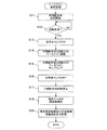
次に、図6〜図13を参照して、カラー画像形成装置100の動作を説明する。先ず、図6〜図8を参照して、ベースライン測定処理を説明する。図6に、ベースライン測定処理の流れを示す。
Next, the operation of the color
カラー画像形成装置100において、例えば、操作部16を介してユーザからベースライン測定処理の実行指示が入力されたことをトリガとして、全体制御部151によりベースライン測定処理が実行される。
In the color
図6に示すように、先ず、中間転写体6がエンジン制御部157を介して回転駆動開始される(ステップS11)。そして、図示しない速度センサの検知により、中間転写体6の回転速度が測定され、その回転速度が安定しているか否かが判別される(ステップS12)。回転速度が安定していない場合は(ステップS12;NO)、ステップS12に移行する。そして、図示しない速度センサの検知により、中間転写体6の回転速度が測定され、その回転速度が安定しているか否かが判別される(ステップS12)。回転速度が安定している場合は(ステップS12;YES)、光学式センサ12A,12Bがオンされ、中間転写体6の表面検知が開始される(ステップS13)。
As shown in FIG. 6, first, the intermediate transfer member 6 is started to rotate via the engine control unit 157 (step S11). Then, the rotation speed of the intermediate transfer body 6 is measured by detection of a speed sensor (not shown), and it is determined whether or not the rotation speed is stable (step S12). If the rotational speed is not stable (step S12; NO), the process proceeds to step S12. Then, the rotation speed of the intermediate transfer body 6 is measured by detection of a speed sensor (not shown), and it is determined whether or not the rotation speed is stable (step S12). When the rotation speed is stable (step S12; YES), the
そして、ベルトN回転分(N:予め設定された自然数)のベースライン補正が実行される(ステップS14)。ベースライン補正とは、中間転写体6を長期間使用すると、中間転写体6表面の粗さが変化するため、光学式センサ12A,12Bの出力電圧も大きく変動するようになり、後述する濃度パッチのトナー付着量を正確に測定できなくなってしまうので、中間転写体6のトナー付着特性のバラツキを一定レベル以下にすることを目的として、後述する補正用画像形成前に行なう補正である。
Then, baseline correction is performed for the belt N rotation (N: a preset natural number) (step S14). Baseline correction means that when the intermediate transfer member 6 is used for a long period of time, the roughness of the surface of the intermediate transfer member 6 changes, so that the output voltages of the
ベースライン補正としては、光学式センサ12A,12Bで中間転写体6のトナー付着の無い領域、所謂ベースラインを全周に渡って検知することでその特性を認識し、現像装置4Y,4M,4C,4Kの周速比を適宜可変制御することで、トナー付着量を一定に維持させたり、同様に、ベースラインの検知後、光学式センサ12A,12Bの出力電圧の振幅を所定範囲内になるように光学式センサ12A,12Bの発光素子(LED)を光量調整する。
As the baseline correction, the
そして、ベースライン補正後に、光学式センサ12A,12Bにより、N回転分の中間転写体6の表面が検知され、信号処理部153により、光学式センサ12A,12Bの検知信号が離散化され、そのサンプリングデータがRAM154に格納される(ステップS15)。
After the baseline correction, the
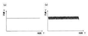
図7(a)に、ベースライン補正後の光学式センサ12A,12Bの理想的な出力波形を示す。図7(b)に、ベースライン補正後の光学式センサ12A,12Bの現実的な出力波形の一例を示す。図7(a)に示すように、光学式センサ12A,12Bの理想的な出力電圧は、時間に対して一定となり、現実的には、図7(b)に示す波形となる。
FIG. 7A shows ideal output waveforms of the
そして、光学式センサ12A,12Bがオフされ、中間転写体6の表面検知が終了される(ステップS16)。そして、中間転写体6がエンジン制御部157を介して回転駆動終了される(ステップS17)。そして、RAM154に格納されたベースラインのサンプリングデータが周波数解析される(ステップS18)。具体的には、時間に対する電圧成分としてのベースラインのサンプリングデータに、FFT(Fast Fourier Transform:高速フーリエ変換)が施され、周波数に対する周波数成分(振幅)の波形が取得される。
Then, the
そして、周波数解析後のデータについて、中間転写体6の傷、ごみによるノイズを特定するため予め設定された所定周波数範囲でのノイズとなる卓越周波数成分が特定され、その卓越周波数が抽出されて不揮発メモリ14に記憶され(ステップS19)、ベースライン測定処理を終了する。 Then, in the data after the frequency analysis, a dominant frequency component that becomes noise in a predetermined frequency range set in advance to identify noise due to scratches and dust on the intermediate transfer body 6 is identified, and the dominant frequency is extracted and nonvolatile The data is stored in the memory 14 (step S19), and the baseline measurement process is terminated.
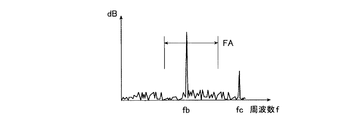
図8に、ベースラインのサンプリングデータの周波数解析後の波形の一例を示す。図8に示すように、周波数に対する周波数成分において、中間転写体6の傷、ごみによるノイズが出やすい周波数範囲FAにおいて、中間転写体6の傷、ごみ起因のノイズが発生している周波数fbが卓越周波数とされる。電気的ノイズ成分の周波数fcは、周波数範囲FA内でないので卓越周波数に特定されない。 FIG. 8 shows an example of a waveform after frequency analysis of baseline sampling data. As shown in FIG. 8, in the frequency component with respect to the frequency, the frequency fb at which noise due to scratches and dust is generated in the intermediate transfer member 6 in the frequency range FA where noise due to scratches and dust is likely to occur. It is regarded as the dominant frequency. The frequency fc of the electrical noise component is not specified as the dominant frequency because it is not within the frequency range FA.
所定周波数範囲としては、中間転写体6の傷、ごみ起因のノイズが発生しうる範囲が経験的に決定及び設定される。また、卓越周波数は、例えば、所定閾値を越えた周波数成分の周波数とする。さらに、卓越周波数、所定周波数範囲は、一つに限定されるものではなく、複数としてもよい。 As the predetermined frequency range, a range in which noise due to scratches and dust on the intermediate transfer body 6 can be generated is determined and set empirically. The dominant frequency is, for example, a frequency component that exceeds a predetermined threshold. Further, the dominant frequency and the predetermined frequency range are not limited to one and may be plural.
次に、図9〜図13を参照して、ベースライン測定処理の後に実行される補正用画像測定処理を説明する。図9に、補正用画像測定処理の流れを示す。 Next, the correction image measurement process executed after the baseline measurement process will be described with reference to FIGS. FIG. 9 shows the flow of the correction image measurement process.
カラー画像形成装置100において、例えば、操作部16を介してユーザから補正用画像測定処理の実行指示が入力されたことをトリガとして、全体制御部151により補正用画像測定処理が実行される。
In the color
図9に示すように、ステップS21,S22は、それぞれ、ベースライン測定処理のステップS11,S12と同様である。回転速度が安定している場合は(ステップS22;YES)、不揮発メモリ14に予め記憶されたレジストマークCR及び濃度パッチPTのの補正用画像データが読み出され、その補正用画像データに基づいて、中間転写体6上に補正用画像のトナー像が形成開始される(ステップS11)。
As shown in FIG. 9, steps S21 and S22 are the same as steps S11 and S12 of the baseline measurement process, respectively. When the rotation speed is stable (step S22; YES), the correction image data of the registration mark CR and the density patch PT stored in advance in the
ステップS24は、ベースライン測定処理のステップS13と同様である。そして、中間転写体6の位置が光学式センサ12A,12Bで補正用画像を検知する位置か否かが判別される(ステップS25)。補正用画像の検知位置でない場合は(ステップS25;NO)、ステップS25に移行される。補正用画像の検知位置である場合は(ステップS25;YES)、光学式センサ12A,12Bにより、補正用画像が形成された中間転写体6の表面が検知され、信号処理部153により、光学式センサ12A,12Bの検知信号が離散化され、そのサンプリングデータがRAM154に格納される(ステップS26)。
Step S24 is the same as step S13 of the baseline measurement process. Then, it is determined whether or not the position of the intermediate transfer body 6 is a position where the
図10(a)に、レジストマークCR検出時の光学式センサ12A,12Bの理想的な出力波形を示す。図11(a)に、レジストマークCR検出時の光学式センサ12A,12Bの現実的な出力波形の一例を示す。図10(a)に示すように、光学式センサ12A,12Bの理想的な出力電圧は、時間に対して凹形となり、現実的には、図11(a)に示す波形となる。
FIG. 10A shows ideal output waveforms of the
ステップS27,S28は、それぞれ、ベースライン測定処理のステップS16,S17と同様である。そして、RAM154に格納された補正用画像のサンプリングデータが周波数解析される(ステップS29)。具体的には、時間に対する電圧成分としての補正用画像のサンプリングデータに、FFTが施され、周波数に対する周波数成分の波形が取得される。
Steps S27 and S28 are the same as steps S16 and S17 of the baseline measurement process, respectively. Then, the sampling data of the correction image stored in the
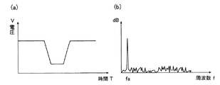
図10(b)に、レジストマークCR検出時の理想的なサンプリングデータの周波数解析後の波形を示す。図11(b)に、レジストマークCR検出時の現実的なサンプリングデータの周波数解析後の波形を示す。図10(b)に示すように、図10(a)に示す理想的なサンプリングデータの周波数解析後の波形は、レジストマークCR検出時特有の周波数faで周波数成分が大きくなっている。図11(b)に示すように、図11(a)に示す現実的なサンプリングデータの周波数解析後の波形は、周波数faと、中間転写体6の傷、ごみによるノイズの周波数fbと、電気的ノイズの周波数fcと、の周波数成分が大きくなっている。 FIG. 10B shows a waveform after frequency analysis of ideal sampling data when the registration mark CR is detected. FIG. 11B shows a waveform after frequency analysis of realistic sampling data when the registration mark CR is detected. As shown in FIG. 10 (b), the ideal sampling data shown in FIG. 10 (a) has a frequency component with a frequency fa characteristic at the time of registration mark CR detection. As shown in FIG. 11B, the waveform after the frequency analysis of the realistic sampling data shown in FIG. 11A includes the frequency fa, the frequency fb of noise due to scratches and dust on the intermediate transfer body 6, and the electrical The frequency component of the natural noise frequency fc is large.
そして、不揮発メモリ14に記憶された卓越周波数が読み出され、周波数解析後の補正用画像のサンプリングデータから卓越周波数成分が削除される(ステップS30)。具体的には、周波数解析後の補正用画像のサンプリングデータの卓越周波数成分に0が代入される。
Then, the dominant frequency stored in the
図12に、補正用画像のサンプリングデータからの卓越周波数成分の削除の一例を示す。図12に示すように、図11(b)に示す周波数解析後の補正用画像のサンプリングデータから、卓越周波数fb成分を削除すると、周波数fa及び周波数fcの周波数成分が大きくなっている周波数解析後の補正用画像のサンプリングデータが得られる。 FIG. 12 shows an example of deleting the dominant frequency component from the sampling data of the correction image. As shown in FIG. 12, when the dominant frequency fb component is deleted from the sampling data of the correction image after frequency analysis shown in FIG. 11B, the frequency components of the frequency fa and the frequency fc are increased. Sampling data of the correction image is obtained.
そして、卓越周波数成分が削除された周波数解析後の補正用画像のサンプリングデータに逆周波数変換が施される(ステップS31)。具体的には、周波数に対する周波数成分の補正用画像のサンプリングデータに、逆FFTが施されて、時間に対する電圧の補正用画像のサンプリングデータに逆変換される。 Then, inverse frequency conversion is performed on the sampling data of the image for correction after frequency analysis from which the dominant frequency component has been deleted (step S31). Specifically, the inverse FFT is applied to the sampling data of the frequency component correction image with respect to the frequency, and the inverse conversion is performed to the sampling data of the voltage correction image with respect to time.
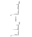
そして、逆周波数変換された補正用画像のサンプリングデータに基づいて、レジストマークCRの位置情報が算出されて不揮発メモリ14に記憶される(ステップS32)。レジストマークの位置情報算出としては、例えば、重心検知により位置情報を特定する方法がある。図13(a)に、2値化されたパターン検出信号を示す。図13(b)に、光学式センサ12A,12Bにより検出されたパターン検出信号の中心位置決定例を示す。
Then, the position information of the registration mark CR is calculated based on the sampling data of the correction image that has been subjected to inverse frequency conversion, and is stored in the nonvolatile memory 14 (step S32). As registration mark position information calculation, for example, there is a method of specifying position information by detecting the center of gravity. FIG. 13A shows a binarized pattern detection signal. FIG. 13B shows an example of determining the center position of the pattern detection signal detected by the
幅D1のパターン(レジストマークCRの一部)をデジタルセンサで検知したときの2値化した検知信号は図13(a)のようになる。同様に、幅D1のパターンをアナログセンサである光学式センサ12A,12Bにより検知したときの検知信号は図13(b)のようになる。図13(a)では、検知信号のHigh成分の中心位置を算出することにより、パターンの中心位置情報が算出される。デジタルセンサは、パターンの中心位置の算出が容易であるが、センサとしてスポット径が小さいものが求められるので、本実施の形態では、光学式センサ12A,12Bとしてアナログセンサを使用している。
A binarized detection signal when a pattern with a width D1 (a part of the registration mark CR) is detected by a digital sensor is as shown in FIG. Similarly, the detection signal when the pattern of the width D1 is detected by the
本実施の形態の例としての図13(b)では、検知信号と所定ラインC1との間の領域の積分値が算出され、その積分値が2等分されて領域A1,A2の面積が等しくなる時間T1に対応する位置がパターンの中心位置情報として算出される。このようにして、レジストマークCRの位置情報が算出される。 In FIG. 13B as an example of the present embodiment, the integral value of the region between the detection signal and the predetermined line C1 is calculated, and the integral value is divided into two, so that the areas of the regions A1 and A2 are equal. The position corresponding to the time T1 is calculated as the center position information of the pattern. In this way, the position information of the registration mark CR is calculated.
そして、逆周波数変換された補正用画像のサンプリングデータに基づいて、濃度パッチPTの各パッチの濃度情報が算出されて不揮発メモリ14に記憶され(ステップS33)、補正用画像測定処理が終了する。ステップS33は、具体的には、濃度パッチPTの各パッチのサンプリングデータの平均値が算出され、その平均値がそのパッチの濃度情報として特定される。 Then, the density information of each patch of the density patch PT is calculated based on the sampling data of the correction image subjected to inverse frequency conversion and stored in the nonvolatile memory 14 (step S33), and the correction image measurement process is completed. In step S33, specifically, an average value of sampling data of each patch of the density patch PT is calculated, and the average value is specified as density information of the patch.
補正用画像測定処理の実行後に、不揮発メモリ14に記憶されたレジストマークCRの位置情報に基づいて、主走査補正量算出部1521、副走査補正量算出部1522、全体横倍補正量算出部1523、部分横倍補正量算出部1524、スキュー補正量算出部1525により、それぞれ、主走査補正量、副走査補正量、全体横倍補正量、部分横倍補正量、スキュー補正量が算出されて、レジスト補正用LUTが算出され、不揮発メモリ14に記憶されたレジスト補正用LUTが更新される。その主走査補正量、副走査補正量、全体横倍補正量、部分横倍補正量、スキュー補正量に基づいて、主走査開始タイミング制御部1551、副走査開始タイミング制御部1552、画素クロック周期制御部1553、書き込みユニット駆動部1554、画像形成ユニット駆動部1555により、それぞれ、主走査補正処理、副走査補正処理、全体横倍補正処理、部分横倍補正処理、スキュー補正処理が実行される。
After executing the correction image measurement processing, based on the registration mark CR position information stored in the
また、補正用画像測定処理の実行後に、不揮発メモリ14に記憶された濃度情報に基づいて、階調補正量算出部1526により、階調補正量(階調補正用LUT)が算出されて不揮発メモリ14に記憶された階調補正量が更新される。その階調補正量に基づいて、階調制御部1556により、階調補正処理が実行される。
In addition, after the correction image measurement process is executed, a gradation correction amount (tone correction LUT) is calculated by the gradation correction
以上、本実施の形態によれば、ベースライン測定時に、画像形成されていない中間転写体6の表面を光学式センサ12A,12Bで検知し、そのベースラインの検知信号を離散化し周波数解析し、その解析信号から、中間転写体6の傷、ごみに起因するノイズに対応する卓越周波数を抽出するので、その卓越周波数を補正用画像の検知信号に用いることで、補正用画像の検知信号から、中間転写体6の傷、ごみに起因するノイズの卓越周波数成分を容易且つ高精度に削除できる。
As described above, according to the present embodiment, at the time of baseline measurement, the surface of the intermediate transfer body 6 on which no image is formed is detected by the
また、ベースラインの検知信号からの卓越周波数の抽出を所定の周波数範囲内で行うことにより、例えば全ての周波数から卓越周波数を抽出する場合に比べて、卓越周波数の抽出時間を低減できる。 Further, by extracting the dominant frequency from the baseline detection signal within a predetermined frequency range, for example, the extraction time of the dominant frequency can be reduced as compared with the case of extracting the dominant frequency from all frequencies.
また、補正画像測定時に、補正画像を中間転写体6に画像形成し、その中間転写体6の表面を光学式センサ12A,12Bで検知し、そのベースラインの検知信号を離散化し周波数解析し、その解析信号から、中間転写体6の傷、ごみに起因するノイズに対応する卓越周波数成分を削除するので、補正用画像の検知信号から、中間転写体6の傷、ごみに起因するノイズの卓越周波数成分を容易且つ高精度に削除できる。
Further, when the corrected image is measured, the corrected image is formed on the intermediate transfer body 6, the surface of the intermediate transfer body 6 is detected by the
また、補正用画像の濃度パッチPTの検知により算出される卓越周波数成分を削除した検知信号に基づいて、濃度情報を算出するので、その濃度情報に基づいて、階調補正量算出部1526により階調補正量を算出でき、不揮発メモリ14に記憶された階調補正量(階調補正用LUT)を更新できる。特に、中間転写体6の傷、ごみが目立つ濃度パッチPTの薄い濃度部分に対応する傷、ごみに起因するノイズの卓越周波数成分を良好に削除できる。
Further, since the density information is calculated based on the detection signal from which the dominant frequency component calculated by detecting the density patch PT of the correction image is deleted, the gradation correction
また、補正用画像のレジストマークCRの検知により算出される卓越周波数成分を削除した検知信号に基づいて、レジストマークCRの位置情報を算出するので、そのレジストマークCRの位置情報に基づいて、補正量演算部152によりレジスト補正量を算出でき、不揮発メモリ14に記憶されたレジスト補正量(レジスト補正用LUT)を更新できる。
Further, since the position information of the registration mark CR is calculated based on the detection signal from which the dominant frequency component calculated by detecting the registration mark CR of the correction image is deleted, the correction is performed based on the position information of the registration mark CR. The
なお、上記実施の形態における記述は、本発明に係る好適な信号処理装置及び画像形成装置の一例であり、これに限定されるものではない。 The description in the above embodiment is an example of a suitable signal processing apparatus and image forming apparatus according to the present invention, and the present invention is not limited to this.
例えば、上記実施の形態では、卓越周波数として中間転写体6の傷、ごみ起因のノイズに対応する周波数を抽出したが、これに限定されるものではない。例えば、電気的ノイズに対応する周波数を卓越周波数とする構成としてもよい。 For example, in the above-described embodiment, the frequency corresponding to the scratch on the intermediate transfer body 6 and noise caused by dust is extracted as the dominant frequency, but the present invention is not limited to this. For example, the frequency corresponding to the electrical noise may be a dominant frequency.
また、上記実施の形態では、記録媒体としての中間転写体6に補正用画像を形成する構成としたが、記録用紙、OHPシート等の記録シート上に補正用画像を形成し、その記録シートを光学式センサで検知し、その検知信号から卓越周波数成分を削除する構成としてもよい。 In the above embodiment, the correction image is formed on the intermediate transfer member 6 as a recording medium. However, the correction image is formed on a recording sheet such as a recording sheet or an OHP sheet, and the recording sheet is used. It is good also as a structure which detects with an optical sensor and deletes a dominant frequency component from the detection signal.
また、以上の実施の形態におけるカラー画像形成装置100を構成する各部の細部構成及び細部動作に関して本発明の趣旨を逸脱することのない範囲で適宜変更可能である。
Further, the detailed configuration and detailed operation of each part constituting the color
1Y,1M,1C,1K 感光体ドラム
2Y,2M,2C,2K 帯電手段
3Y,3M,3C,3K 画像書き込みユニット
4Y,4M,4C,4K 現像装置
5Y,5M,5C 補正手段
6 中間転写体
7A 2次転写ローラ
7Y,7M,7C,7K 1次転写ローラ
8A 中間転写体用クリーニング手段
8Y,8M,8C,8K 感光体ドラム用クリーニング手段
9Y スキュー調整手段
10Y,10M,10C,10K 画像形成ユニット
12A,12B 光学式センサ
14 不揮発メモリ
15 制御手段
151 全体制御部
152 補正量演算部
153 信号処理部
154 RAM
155 書き込み制御部
1551 主走査開始タイミング制御部
1552 副走査開始タイミング制御部
1553 画素クロック周期制御部
1554 書き込みユニット駆動部
1555 画像形成ユニット駆動部
1556 階調制御部
156 読み取り制御部
157 エンジン制御部
158 通信制御部
16 操作部
17 定着装置
18 表示部
20A,20B,20C 給紙カセット
21 送り出しローラ
22A 給紙ローラ
22B,22C,22D 搬送ローラ
23 レジストローラ
24 排紙ローラ
25 排紙トレイ
26 分岐手段
27A 循環通紙路
27B 反転搬送路
27C 再給紙搬送部
31 半導体レーザ光源
32 コリメータレンズ
33 補助レンズ
34 ポリゴンミラー
35 ポリゴンモータ
36 f(θ)レンズ
37 ミラー面結像用CY1レンズ
38 ドラム面結像用CY2レンズ
39 反射板
41 調整ギヤユニット
42 調整用モータ
45 ポリゴンモータ駆動基板
46 LD駆動基板
49 レーザインデックスセンサ
50 画像メモリ
70 画像処理手段
71 画像処理回路
72C C−信号切換部
72K K−信号切換部
72M M−信号切換部
72Y Y−信号切換部
100 カラー画像形成装置
101 画像形成装置本体
102 画像読取装置
103 画像形成手段
201 自動原稿給紙装置
202 原稿画像走査露光装置
1Y, 1M, 1C, 1K Photosensitive drums 2Y, 2M, 2C, 2K Charging means 3Y, 3M, 3C, 3K
155
Claims (7)
前記補正用画像が形成されていない前記記録媒体の表面を前記光学式センサに検知させ、当該光学式センサから出力される検知信号に周波数解析を行い、その第1の解析信号から他の値よりも卓越した周波数成分に対応する卓越周波数を抽出し、前記補正用画像が形成された前記記録媒体の表面を前記光学式センサに検知させ、当該光学式センサから出力される検知信号に周波数解析を行い、その第2の解析信号から前記卓越周波数の成分を削除し、当該卓越周波数成分を削除した解析信号に逆周波数変換を行い当該卓越周波数成分を削除した検知信号を算出する制御手段と、を備えることを特徴とする信号処理装置。 An optical sensor that detects the surface of the recording medium on which a correction image is to be formed and outputs a detection signal;
The optical sensor detects the surface of the recording medium on which the image for correction is not formed, performs frequency analysis on the detection signal output from the optical sensor, and determines other values from the first analysis signal. Also extracts the dominant frequency corresponding to the outstanding frequency component, causes the optical sensor to detect the surface of the recording medium on which the correction image is formed, and performs frequency analysis on the detection signal output from the optical sensor. And a control means for deleting the dominant frequency component from the second analysis signal, performing inverse frequency conversion on the analysis signal from which the dominant frequency component has been deleted, and calculating a detection signal from which the dominant frequency component has been deleted. A signal processing apparatus comprising:
前記制御手段は、前記濃度パッチの検知により算出される前記卓越周波数成分を削除した検知信号に基づいて、濃度情報を算出することを特徴とする請求項1又は2に記載の信号処理装置。 The correction image includes a density patch for density correction for image formation,
The signal processing apparatus according to claim 1, wherein the control unit calculates density information based on a detection signal from which the dominant frequency component calculated by detecting the density patch is deleted.
前記制御手段は、前記レジストマークの検知により算出される前記卓越周波数成分を削除した検知信号に基づいて、前記レジストマークの位置情報を算出することを特徴とする請求項1から3のいずれか一項に記載の信号処理装置。 The correction image includes a registration mark for image formation registration correction,
The said control means calculates the positional information on the said registration mark based on the detection signal which deleted the said dominant frequency component calculated by the detection of the said registration mark. The signal processing device according to item.
前記記録媒体に画像形成する画像形成手段と、を備え、
前記補正用画像は、前記画像形成手段により画像形成されることを特徴とする画像形成装置。 A signal processing device according to any one of claims 1 to 6;
Image forming means for forming an image on the recording medium,
The image forming apparatus, wherein the image for correction is formed by the image forming unit.
Priority Applications (2)
| Application Number | Priority Date | Filing Date | Title |
|---|---|---|---|
| JP2006020680A JP2007196621A (en) | 2006-01-30 | 2006-01-30 | Signal processing device and imaging device |
| US11/586,685 US7777896B2 (en) | 2006-01-30 | 2006-10-26 | Signal processing apparatus and image forming apparatus |
Applications Claiming Priority (1)
| Application Number | Priority Date | Filing Date | Title |
|---|---|---|---|
| JP2006020680A JP2007196621A (en) | 2006-01-30 | 2006-01-30 | Signal processing device and imaging device |
Publications (1)
| Publication Number | Publication Date |
|---|---|
| JP2007196621A true JP2007196621A (en) | 2007-08-09 |
Family
ID=38322208
Family Applications (1)
| Application Number | Title | Priority Date | Filing Date |
|---|---|---|---|
| JP2006020680A Pending JP2007196621A (en) | 2006-01-30 | 2006-01-30 | Signal processing device and imaging device |
Country Status (2)
| Country | Link |
|---|---|
| US (1) | US7777896B2 (en) |
| JP (1) | JP2007196621A (en) |
Cited By (7)
| Publication number | Priority date | Publication date | Assignee | Title |
|---|---|---|---|---|
| JP2009042473A (en) * | 2007-08-08 | 2009-02-26 | Canon Inc | Image forming apparatus |
| JP2009080246A (en) * | 2007-09-26 | 2009-04-16 | Kyocera Mita Corp | Image forming apparatus |
| JP2009166413A (en) * | 2008-01-18 | 2009-07-30 | Ricoh Co Ltd | Image forming apparatus |
| JP2010211197A (en) * | 2009-02-13 | 2010-09-24 | Canon Inc | Image forming apparatus |
| JP2011180446A (en) * | 2010-03-02 | 2011-09-15 | Canon Inc | Image forming apparatus, and control method and program of the same |
| JP2012048231A (en) * | 2010-08-25 | 2012-03-08 | Xerox Corp | Dual registration and process control toned patches |
| JP2014048302A (en) * | 2012-08-29 | 2014-03-17 | Kyocera Document Solutions Inc | Image forming device and calibration method |
Families Citing this family (5)
| Publication number | Priority date | Publication date | Assignee | Title |
|---|---|---|---|---|
| JP4882925B2 (en) * | 2007-08-31 | 2012-02-22 | セイコーエプソン株式会社 | Image data processing apparatus and image data processing method |
| JP2009274320A (en) * | 2008-05-14 | 2009-11-26 | Canon Inc | Image forming apparatus and its control method |
| US8736894B2 (en) * | 2011-12-20 | 2014-05-27 | Eastman Kodak Company | Producing correction data for printer |
| KR102144316B1 (en) * | 2013-07-18 | 2020-08-13 | 휴렛-팩커드 디벨롭먼트 컴퍼니, 엘.피. | Image forming apparatus and method for color registration correction |
| JP6756171B2 (en) * | 2016-07-11 | 2020-09-16 | コニカミノルタ株式会社 | Image processing equipment, image forming equipment, image forming system, and image processing program |
Citations (4)
| Publication number | Priority date | Publication date | Assignee | Title |
|---|---|---|---|---|
| JPH04337754A (en) * | 1991-05-14 | 1992-11-25 | Canon Inc | Image forming device |
| JPH08286457A (en) * | 1995-04-19 | 1996-11-01 | Fuji Xerox Co Ltd | Image forming device |
| JP2005018094A (en) * | 1997-09-03 | 2005-01-20 | Fuji Xerox Co Ltd | Method for detection image deviation and image density and color image forming apparatus |
| JP2005208422A (en) * | 2004-01-23 | 2005-08-04 | Fuji Xerox Co Ltd | Fixing roll streak inspecting device and control device |
Family Cites Families (5)
| Publication number | Priority date | Publication date | Assignee | Title |
|---|---|---|---|---|
| US5121230A (en) * | 1987-01-19 | 1992-06-09 | Canon Kabushiki Kaisha | Image reading apparatus having adjusting circuits for matching the level of and compensating for fluctuation among a plurality of sensing elements |
| JP3621288B2 (en) * | 1999-04-16 | 2005-02-16 | シャープ株式会社 | Image processing device |
| JP2001265086A (en) | 2000-03-22 | 2001-09-28 | Matsushita Electric Ind Co Ltd | Color image forming equipment |
| JP3640629B2 (en) | 2001-09-21 | 2005-04-20 | 株式会社リコー | Color image forming apparatus |
| US6975338B2 (en) * | 2002-05-31 | 2005-12-13 | Ricoh Company, Ltd. | Image quality detecting apparatus, image forming apparatus and method, and image quality controlling apparatus and method |
-
2006
- 2006-01-30 JP JP2006020680A patent/JP2007196621A/en active Pending
- 2006-10-26 US US11/586,685 patent/US7777896B2/en not_active Expired - Fee Related
Patent Citations (4)
| Publication number | Priority date | Publication date | Assignee | Title |
|---|---|---|---|---|
| JPH04337754A (en) * | 1991-05-14 | 1992-11-25 | Canon Inc | Image forming device |
| JPH08286457A (en) * | 1995-04-19 | 1996-11-01 | Fuji Xerox Co Ltd | Image forming device |
| JP2005018094A (en) * | 1997-09-03 | 2005-01-20 | Fuji Xerox Co Ltd | Method for detection image deviation and image density and color image forming apparatus |
| JP2005208422A (en) * | 2004-01-23 | 2005-08-04 | Fuji Xerox Co Ltd | Fixing roll streak inspecting device and control device |
Cited By (8)
| Publication number | Priority date | Publication date | Assignee | Title |
|---|---|---|---|---|
| JP2009042473A (en) * | 2007-08-08 | 2009-02-26 | Canon Inc | Image forming apparatus |
| JP2009080246A (en) * | 2007-09-26 | 2009-04-16 | Kyocera Mita Corp | Image forming apparatus |
| JP2009166413A (en) * | 2008-01-18 | 2009-07-30 | Ricoh Co Ltd | Image forming apparatus |
| JP2010211197A (en) * | 2009-02-13 | 2010-09-24 | Canon Inc | Image forming apparatus |
| JP2011180446A (en) * | 2010-03-02 | 2011-09-15 | Canon Inc | Image forming apparatus, and control method and program of the same |
| US8717639B2 (en) | 2010-03-02 | 2014-05-06 | Canon Kabushiki Kaisha | Image processing for position deviation correction |
| JP2012048231A (en) * | 2010-08-25 | 2012-03-08 | Xerox Corp | Dual registration and process control toned patches |
| JP2014048302A (en) * | 2012-08-29 | 2014-03-17 | Kyocera Document Solutions Inc | Image forming device and calibration method |
Also Published As
| Publication number | Publication date |
|---|---|
| US20070177889A1 (en) | 2007-08-02 |
| US7777896B2 (en) | 2010-08-17 |
Similar Documents
| Publication | Publication Date | Title |
|---|---|---|
| JP2007196621A (en) | Signal processing device and imaging device | |
| US20080253781A1 (en) | Color image forming apparatus and control method therefor | |
| JP2007199211A (en) | Image forming apparatus and image forming method | |
| JP2006195176A (en) | Image forming apparatus and image forming method | |
| JP2007264439A (en) | Image forming apparatus, toner concentration adjustment method, program and recording medium for image forming apparatus | |
| JP4869692B2 (en) | Image forming apparatus, color misregistration correction method, and color misregistration correction program | |
| JP5772335B2 (en) | Image forming apparatus, method and program, and computer-readable storage medium | |
| JP4676746B2 (en) | Drive control device and image forming apparatus | |
| JP2007148080A (en) | Color image forming apparatus | |
| JP2005326806A (en) | Color image forming apparatus | |
| US9310744B1 (en) | Image forming apparatus and method for correcting color misregistration by the same | |
| JP2007298868A (en) | Image forming apparatus and image forming method | |
| JP5364985B2 (en) | Image forming apparatus | |
| JP4770624B2 (en) | Color image forming apparatus | |
| JP2005173253A (en) | Image forming apparatus | |
| JP2009047719A (en) | Image forming apparatus and program | |
| JP2005165220A (en) | Color image forming apparatus and image forming method | |
| JP2006163078A (en) | Apparatus and method for image formation | |
| JP2013161015A (en) | Image forming apparatus | |
| JP4635716B2 (en) | Image forming apparatus and image forming method | |
| JP5222623B2 (en) | Image forming apparatus | |
| JP2002214854A (en) | Image forming device | |
| JP3518825B2 (en) | Image forming device | |
| JP2005003830A (en) | Image forming device | |
| JP2007240592A (en) | Image forming apparatus and displacement correction method for image forming method |
Legal Events
| Date | Code | Title | Description |
|---|---|---|---|
| A621 | Written request for application examination |
Free format text: JAPANESE INTERMEDIATE CODE: A621 Effective date: 20080924 |
|
| A977 | Report on retrieval |
Free format text: JAPANESE INTERMEDIATE CODE: A971007 Effective date: 20110114 |
|
| A131 | Notification of reasons for refusal |
Free format text: JAPANESE INTERMEDIATE CODE: A131 Effective date: 20110118 |
|
| A02 | Decision of refusal |
Free format text: JAPANESE INTERMEDIATE CODE: A02 Effective date: 20111025 |