JP2007173597A - Magnetic memory - Google Patents
Magnetic memory Download PDFInfo
- Publication number
- JP2007173597A JP2007173597A JP2005370440A JP2005370440A JP2007173597A JP 2007173597 A JP2007173597 A JP 2007173597A JP 2005370440 A JP2005370440 A JP 2005370440A JP 2005370440 A JP2005370440 A JP 2005370440A JP 2007173597 A JP2007173597 A JP 2007173597A
- Authority
- JP
- Japan
- Prior art keywords
- layer
- wiring
- magnetic
- magnetization
- current
- Prior art date
- Legal status (The legal status is an assumption and is not a legal conclusion. Google has not performed a legal analysis and makes no representation as to the accuracy of the status listed.)
- Pending
Links
- 230000005291 magnetic effect Effects 0.000 title claims abstract description 210
- 230000015654 memory Effects 0.000 title claims abstract description 72
- 230000005415 magnetization Effects 0.000 claims abstract description 132
- 238000002347 injection Methods 0.000 claims abstract description 29
- 239000007924 injection Substances 0.000 claims abstract description 29
- 230000000694 effects Effects 0.000 claims description 57
- 238000003860 storage Methods 0.000 claims description 31
- 230000005389 magnetism Effects 0.000 claims 1
- 239000000243 solution Substances 0.000 abstract 1
- 239000010410 layer Substances 0.000 description 247
- 229920002120 photoresistant polymer Polymers 0.000 description 33
- 230000005294 ferromagnetic effect Effects 0.000 description 32
- 238000000034 method Methods 0.000 description 20
- 238000004519 manufacturing process Methods 0.000 description 15
- 239000000758 substrate Substances 0.000 description 14
- 238000012546 transfer Methods 0.000 description 14
- 239000000696 magnetic material Substances 0.000 description 13
- 239000004065 semiconductor Substances 0.000 description 13
- 238000004544 sputter deposition Methods 0.000 description 13
- 239000003302 ferromagnetic material Substances 0.000 description 12
- 230000008859 change Effects 0.000 description 11
- 239000010408 film Substances 0.000 description 11
- 229910003321 CoFe Inorganic materials 0.000 description 10
- 239000000463 material Substances 0.000 description 10
- 229910052727 yttrium Inorganic materials 0.000 description 10
- 229910004298 SiO 2 Inorganic materials 0.000 description 8
- 230000005290 antiferromagnetic effect Effects 0.000 description 8
- 229910052715 tantalum Inorganic materials 0.000 description 6
- 229910001030 Iron–nickel alloy Inorganic materials 0.000 description 5
- 238000000151 deposition Methods 0.000 description 4
- 238000010586 diagram Methods 0.000 description 4
- GUVRBAGPIYLISA-UHFFFAOYSA-N tantalum atom Chemical compound [Ta] GUVRBAGPIYLISA-UHFFFAOYSA-N 0.000 description 4
- -1 IrMn Inorganic materials 0.000 description 3
- 229910052802 copper Inorganic materials 0.000 description 3
- 230000008878 coupling Effects 0.000 description 3
- 238000010168 coupling process Methods 0.000 description 3
- 238000005859 coupling reaction Methods 0.000 description 3
- 230000010365 information processing Effects 0.000 description 3
- 229910018072 Al 2 O 3 Inorganic materials 0.000 description 2
- 229910015136 FeMn Inorganic materials 0.000 description 2
- 229910003289 NiMn Inorganic materials 0.000 description 2
- 229910019041 PtMn Inorganic materials 0.000 description 2
- 229910052782 aluminium Inorganic materials 0.000 description 2
- 230000004888 barrier function Effects 0.000 description 2
- 238000005229 chemical vapour deposition Methods 0.000 description 2
- 230000007423 decrease Effects 0.000 description 2
- 230000008021 deposition Effects 0.000 description 2
- 238000011161 development Methods 0.000 description 2
- 239000007772 electrode material Substances 0.000 description 2
- 238000005530 etching Methods 0.000 description 2
- 230000003993 interaction Effects 0.000 description 2
- 230000001590 oxidative effect Effects 0.000 description 2
- 230000010287 polarization Effects 0.000 description 2
- 239000002356 single layer Substances 0.000 description 2
- 239000000126 substance Substances 0.000 description 2
- 239000010409 thin film Substances 0.000 description 2
- 229910052719 titanium Inorganic materials 0.000 description 2
- 229910052723 transition metal Inorganic materials 0.000 description 2
- 150000003624 transition metals Chemical class 0.000 description 2
- 238000002834 transmittance Methods 0.000 description 2
- 229910015371 AuCu Inorganic materials 0.000 description 1
- 229910019236 CoFeB Inorganic materials 0.000 description 1
- 229910019233 CoFeNi Inorganic materials 0.000 description 1
- 229910018979 CoPt Inorganic materials 0.000 description 1
- 230000009471 action Effects 0.000 description 1
- 229910045601 alloy Inorganic materials 0.000 description 1
- 239000000956 alloy Substances 0.000 description 1
- 239000002885 antiferromagnetic material Substances 0.000 description 1
- 230000015572 biosynthetic process Effects 0.000 description 1
- 239000011248 coating agent Substances 0.000 description 1
- 238000000576 coating method Methods 0.000 description 1
- 238000004891 communication Methods 0.000 description 1
- 230000003247 decreasing effect Effects 0.000 description 1
- 238000013461 design Methods 0.000 description 1
- 230000001066 destructive effect Effects 0.000 description 1
- 238000005516 engineering process Methods 0.000 description 1
- 230000005669 field effect Effects 0.000 description 1
- 230000004907 flux Effects 0.000 description 1
- 230000020169 heat generation Effects 0.000 description 1
- 230000006872 improvement Effects 0.000 description 1
- 239000012535 impurity Substances 0.000 description 1
- 238000009413 insulation Methods 0.000 description 1
- 230000010354 integration Effects 0.000 description 1
- 229910052742 iron Inorganic materials 0.000 description 1
- 239000011159 matrix material Substances 0.000 description 1
- 229910052751 metal Inorganic materials 0.000 description 1
- 239000002184 metal Substances 0.000 description 1
- 229910052759 nickel Inorganic materials 0.000 description 1
- 150000004767 nitrides Chemical class 0.000 description 1
- 230000003647 oxidation Effects 0.000 description 1
- 238000007254 oxidation reaction Methods 0.000 description 1
- 230000001681 protective effect Effects 0.000 description 1
- 230000009467 reduction Effects 0.000 description 1
- 238000002310 reflectometry Methods 0.000 description 1
- 230000002040 relaxant effect Effects 0.000 description 1
- 229910052707 ruthenium Inorganic materials 0.000 description 1
- 238000007789 sealing Methods 0.000 description 1
- 230000035945 sensitivity Effects 0.000 description 1
- 229910052710 silicon Inorganic materials 0.000 description 1
- 239000010703 silicon Substances 0.000 description 1
- 229910052721 tungsten Inorganic materials 0.000 description 1
- 229910052725 zinc Inorganic materials 0.000 description 1
Images


Landscapes
- Hall/Mr Elements (AREA)
- Mram Or Spin Memory Techniques (AREA)
- Semiconductor Memories (AREA)
Abstract
Description
本発明は、磁気メモリに関する。 The present invention relates to a magnetic memory.
現在、コンピュータや通信機器などの情報処理装置に用いられている汎用メモリとしてはDRAM、SRAMなどの揮発性メモリが使用されている。しかしながら、DRAMなどの揮発性メモリでは、記憶を保持するためにリフレッシュを行うなど、絶えず電流を供給しておく必要が有り、また、電源を切った場合、全ての情報が失われる。そのため、情報を記憶する手段、すなわち、不揮発性のメモリを別に設ける必要が有り、フラッシュEEPROMやハードディスク装置などが現在用いられている。これら不揮発性メモリにおいては情報処理の高速化に伴ってアクセスの高速化が重要な課題となっている。 Currently, volatile memories such as DRAMs and SRAMs are used as general-purpose memories used in information processing apparatuses such as computers and communication devices. However, in a volatile memory such as a DRAM, it is necessary to continuously supply a current, for example, to refresh the memory, and when the power is turned off, all information is lost. For this reason, it is necessary to provide a means for storing information, that is, a non-volatile memory, and flash EEPROMs and hard disk devices are currently used. In these nonvolatile memories, speeding up access is an important issue as information processing speeds up.
しかしながら、これらの不揮発性メモリはアクセス速度、信頼性、消費電力などの点で、いまだ不十分である。 However, these nonvolatile memories are still insufficient in terms of access speed, reliability, power consumption, and the like.
さらに携帯情報機器の急速な普及および高性能化にともない、いつでも何処でも情報処理が行える、いわゆるユビキタスコンピューティングを目指した情報機器の開発が急速に進められている。この様な機器の開発におけるキーデバイスとして、信頼性の高い高速、大容量不揮発メモリの開発が強く求められている。 In addition, with the rapid spread of portable information devices and higher performance, information devices aiming at so-called ubiquitous computing that can perform information processing anywhere at any time are being rapidly developed. As a key device in the development of such a device, development of a reliable, high-speed, large-capacity nonvolatile memory is strongly demanded.
不揮発メモリの高速化に有効な技術としては、強磁性体層の磁化容易軸に沿った磁化の方向によって情報を記憶する磁性薄膜素子が、マトリックス状に配列されたMRAM(Magnetic Random Access Memory)が有望視されている。MRAMでは2つの強磁性体の、磁化の向きによって情報を記憶する。微小な強磁性体の磁化反転速度は2nsec以下と言われており、高速メモリとしての可能性がある。記憶情報の読み出しには、基準の磁化の向きに対して、感磁層の磁化の向きが、平行化か反並行かによる抵抗変化が生じるのを電流または電圧の変化として検出する。 As an effective technique for increasing the speed of the nonvolatile memory, there is an MRAM (Magnetic Random Access Memory) in which magnetic thin film elements that store information according to the direction of magnetization along the easy axis of the ferromagnetic layer are arranged in a matrix. Promising. In the MRAM, information is stored according to the magnetization directions of two ferromagnetic materials. The magnetization reversal speed of a minute ferromagnet is said to be 2 nsec or less, and there is a possibility as a high-speed memory. In reading the stored information, a change in resistance depending on whether the magnetization direction of the magnetosensitive layer is parallel or antiparallel to the reference magnetization direction is detected as a change in current or voltage.
MRAMには、巨大磁気抵抗(GMR;Giant Magnetoresistance)効果を用いるものがある。GMR効果を用いたMRAMとしては、特許文献1に示されたものが知られている。GMR効果とは、磁化容易軸に平行な2つの磁性層の磁化方向が平行な場合に抵抗値が最小になり、反平行の場合最大になる現象である。GMR効果を用いたMRAMには2つの強磁性体の保持力の差を利用して情報を書き込み/読み出しをおこなうPseudo spin valve型、非磁性層を挟んで反強磁性層との反強磁性結合により磁化方向を固定し固定層と外部磁界により磁化方向が変わる自由層をもったSpin Valve型がある。
Some MRAMs use a giant magnetoresistance (GMR) effect. As an MRAM using the GMR effect, the one disclosed in
GMR効果を用いたMRAMでは抵抗値の変化を電流値または電圧値の変化により読み取る。また、いずれの場合も情報を書き込むためには、配線を流れる電流による誘導磁界(電流磁界)により磁性層の磁化方向を反転させる方法が取られている。 In the MRAM using the GMR effect, a change in resistance value is read by a change in current value or voltage value. In any case, in order to write information, a method of reversing the magnetization direction of the magnetic layer by an induced magnetic field (current magnetic field) due to a current flowing through the wiring is used.
GMRでの抵抗変化をさらに改善するために、強磁性トンネル(TMR;Tunnel Magnetoresistance)効果を利用したMRAMが提案されている。TMR効果は、薄い絶縁層を挟んだ2つの強磁性層間の、磁化方向の相対角度により絶縁層を介して流れるトンネル電流が変化する現象である。磁化方向が平行な場合に抵抗値が最小になり、反平行の場合最大になる。TMRでは例えばCoFe/Al酸化物/CoFeにおいて抵抗変化率40%以上と大きく、また抵抗値が高いため、MOS−FETなどの半導体デバイスと組み合わせた場合のインピダンスマッチングが取りやすい。そのため、GMRと比較して高出力化が容易で、記憶容量やアクセス速度の向上が期待されている。TMR効果を用いたMRAMは、特許文献2及び特許文献3に記載されている。
In order to further improve resistance change in GMR, an MRAM using a ferromagnetic tunnel (TMR) effect has been proposed. The TMR effect is a phenomenon in which a tunnel current flowing through an insulating layer changes depending on the relative angle of the magnetization direction between two ferromagnetic layers sandwiching a thin insulating layer. The resistance value is minimized when the magnetization directions are parallel, and is maximized when the magnetization directions are antiparallel. TMR, for example, has a large resistance change rate of 40% or more in CoFe / Al oxide / CoFe and has a high resistance value, and therefore impedance matching when combined with a semiconductor device such as a MOS-FET can be easily obtained. Therefore, it is easy to increase the output as compared with GMR, and improvement in storage capacity and access speed is expected. The MRAM using the TMR effect is described in
TMR効果を用いたMRAMでは、配線の電流磁界により、磁性膜の磁化方向を所定の方向に変化させて情報を記憶する方法が取られている。記憶された情報の読み出しには、絶縁層に垂直な方向に電流を流し、薄膜磁性素子の抵抗値の変化を検出することによって情報を読み出す方法が取られている。 In the MRAM using the TMR effect, a method of storing information by changing the magnetization direction of the magnetic film in a predetermined direction by the current magnetic field of the wiring is employed. In order to read the stored information, a method of reading information by passing a current in a direction perpendicular to the insulating layer and detecting a change in the resistance value of the thin film magnetic element is employed.
多くのMRAMは、格子状に配線されたビット線とワード線の交点にTMR素子を配置した構造を有する。通常のTMR素子は、2つの強磁性層間に非磁性層を有する強磁性層/非磁性絶縁層/強磁性層の三層構造からなる。強磁性層は、通常は厚さ10nm以下の遷移金属磁性元素(Fe、Co、Ni)又は遷移金属磁性元素の合金(CoFe、CoFeNi、NiFe等)からなり、非磁性絶縁層は、Al2O3やMgO等からなる。 Many MRAMs have a structure in which TMR elements are arranged at intersections between bit lines and word lines wired in a lattice pattern. A normal TMR element has a three-layer structure of a ferromagnetic layer / nonmagnetic insulating layer / ferromagnetic layer having a nonmagnetic layer between two ferromagnetic layers. The ferromagnetic layer is usually made of a transition metal magnetic element (Fe, Co, Ni) or an alloy of transition metal magnetic elements (CoFe, CoFeNi, NiFe, etc.) having a thickness of 10 nm or less, and the nonmagnetic insulating layer is made of Al 2 O. 3 and MgO.
TMR素子を構成する一方の強磁性層(固定層)は、磁化の向きを固定しており、他方の強磁性層(感磁層又は自由層)は磁化の向きが外部磁界に応じて回転する。なお、固定層の構造としては、反強磁性層(FeMn、IrMn、PtMn、NiMn等)を一方の強磁性層に付与した交換結合型が良く用いられる。 One ferromagnetic layer (fixed layer) constituting the TMR element has a fixed magnetization direction, and the other ferromagnetic layer (magnetic sensitive layer or free layer) rotates in accordance with an external magnetic field. . As the structure of the fixed layer, an exchange coupling type in which an antiferromagnetic layer (FeMn, IrMn, PtMn, NiMn, etc.) is provided to one ferromagnetic layer is often used.
メモリ情報の「1」、「0」は、TMR素子を構成する2つの強磁性体の磁化の向きの状態に応じて、すなわち、磁化の方向が平行であるか、反平行であるかに依存して規定される。これら2つの強磁性体の磁化の向きが反平行の時、磁化の向きが平行の時に比べて、厚み方向の電気抵抗の値が大きい。 “1” and “0” of the memory information depend on the state of the magnetization directions of the two ferromagnetic materials constituting the TMR element, that is, whether the magnetization directions are parallel or antiparallel. It is prescribed as When the magnetization directions of these two ferromagnets are antiparallel, the electric resistance value in the thickness direction is larger than when the magnetization directions are parallel.
したがって、「1」、「0」の情報の読出しは、TMR素子の厚み方向に電流を流し、MR(磁気抵抗)効果によるTMR素子の抵抗値又は電流値を測定することで行う。 Therefore, reading of information of “1” and “0” is performed by passing a current in the thickness direction of the TMR element and measuring the resistance value or current value of the TMR element due to the MR (magnetoresistive) effect.
「1」、「0」の情報の書き込みは、TMR素子近傍に配置した配線に電流を流すことで形成される磁界の作用によって、TMR素子の感磁層の磁化の向きを回転させることで行うことが、従来、行われている。 The writing of information of “1” and “0” is performed by rotating the magnetization direction of the magnetosensitive layer of the TMR element by the action of a magnetic field formed by passing a current through a wiring arranged in the vicinity of the TMR element. This has been done in the past.
素子を高集積化して高密度のメモリの実現を図る場合、磁気抵抗効果素子の微小化に伴って磁性層の長さと厚みの比率が小さくなることにより、反磁界が増大し、磁性体の磁化方向を変えるための磁界強度が増大し、大きな書き込み電流が必要となる。 When a high-density memory is realized by high integration of the element, the demagnetizing field increases due to the reduction in the ratio of the length and thickness of the magnetic layer as the magnetoresistive element is miniaturized, thereby increasing the magnetization of the magnetic material. The strength of the magnetic field for changing the direction increases, and a large write current is required.
書き込み電流を低減するため、感磁層の磁化方向を情報の「1」、「0」に対応するように変える書き込み動作において、磁性体に磁界を印加することによる磁化反転方法の他、スピン偏極電流によるスピントランスファートルクを用いたスピン注入磁化反転が知られている。 In order to reduce the write current, in the write operation for changing the magnetization direction of the magnetosensitive layer so as to correspond to information “1” and “0”, in addition to the magnetization reversal method by applying a magnetic field to the magnetic material, the spin polarization Spin injection magnetization reversal using spin transfer torque by pole current is known.
情報の読み出し方法としては各セルに読み出し選択トランジスタを設け、選択セルの読み出しトランジスタのみを導通状態にして、選択セルの磁気抵抗効果素子の抵抗を読み取る方式が一般的である。 As a method of reading information, generally, a read selection transistor is provided in each cell, and only the read transistor of the selected cell is made conductive to read the resistance of the magnetoresistive effect element of the selected cell.
スピントランスファートルクとは、一方の強磁性体から非磁性層を介して他方の強磁性体に電流を流した場合、他方の強磁性体の磁化方向を変えようとするトルクである。したがって、注入電流のスピンの向きを制御すれば、他方の磁性体の磁化の向きを変更することが可能とされている。 The spin transfer torque is a torque for changing the magnetization direction of the other ferromagnetic material when a current is passed from one ferromagnetic material to the other ferromagnetic material via the nonmagnetic layer. Therefore, by controlling the spin direction of the injection current, it is possible to change the magnetization direction of the other magnetic material.
例えば、微小な強磁性層/非磁性層/強磁性層からなる積層体の膜面に垂直な方向に電流を流すと強磁性体の磁化反転が生じる。この現象はスピン注入磁化反転と呼ばれており、強磁性層と非磁性層との接合面において上向きスピン(アップスピン)の電子と下向きスピン(ダウンスピン)の電子のエネルギー状態が異なるため、アップスピンおよびダウンスピンの電子の透過率や反射率が異なりスピン分極電流が流れる。 For example, when a current is passed in a direction perpendicular to the film surface of a laminate composed of a small ferromagnetic layer / nonmagnetic layer / ferromagnetic layer, magnetization reversal of the ferromagnetic material occurs. This phenomenon is called spin-injection magnetization reversal, and the energy state of up-spin (up spin) and down-spin (down spin) electrons is different at the interface between the ferromagnetic layer and the nonmagnetic layer. Spin transmittance and reflectivity of spin and down spin electrons are different and spin polarization current flows.
強磁性層に流れ込んだスピン分極電流のスピン偏極電子は強磁性層の電子と交換相互作用をして電子間にトルクが発生し磁化反転が生じる。これはオープンな電流磁界による磁化反転とは異なり、磁性体内部の電流により磁化反転がおきるため、隣接セルへの影響が小さく、素子の微小化に伴って書き込み電流が増大しにくく、逆に微小化により書き込み電流を減少させることができる。したがって、情報を記録する方法としてスピン注入磁化反転を用いることにより、高密度の磁気メモリを実現することができる。 The spin-polarized electrons of the spin-polarized current that have flowed into the ferromagnetic layer interact with the electrons in the ferromagnetic layer to generate torque between the electrons, resulting in magnetization reversal. This is different from magnetization reversal due to an open current magnetic field, because magnetization reversal occurs due to the current inside the magnetic material, so the influence on adjacent cells is small, and the write current is unlikely to increase with the miniaturization of the element, and conversely Thus, the write current can be reduced. Therefore, a high-density magnetic memory can be realized by using spin injection magnetization reversal as a method of recording information.
スピントランスファートルクを利用して、強磁性体の磁化の向きを変える方法としては、(I)緩和スイッチ(Relaxing Switching)法、(II)歳差スイッチ(Precessional Switching)法、(III)緩和歳差スイッチ(Relaxing−Precessional Switching)法などが知られている。 Methods for changing the magnetization direction of a ferromagnetic material using spin transfer torque include (I) a relaxation switching method, (II) a precession switching method, and (III) a relaxation precession. A switch (Relaxing-Precisional Switching) method and the like are known.
緩和スイッチ法では、感磁層の磁化の向きを、固定層からのスピントランスファートルクで制御するが、固定層の磁化の向きは膜面内にあり、感磁層の磁化容易軸と平行である。したがって、感磁層の磁化の向きを反転させる場合、反転の初期段階において、スピントランスファートルクと、磁化を有効磁界方向に向けようとするSpin Relaxingが競合する。また、固定層の磁化の向きと感磁層の磁化の向きが平行に近い反転の初期段階では、スピントランスファートルクが小さいため、反転に時間を要する。すなわち、緩和スイッチ法では、これらの力に抗しながら平衡状態へ徐々に磁化の向きを変更させていくので、磁化の向きを反転させるためには、大きな電流が必要となる。磁化反転に必要なスピントランスファートルクの大きさはLLG(Landau−Lifshitz−Gilbert)方程式に含まれるギルバート減衰定数に比例する。 In the relaxation switch method, the magnetization direction of the magnetosensitive layer is controlled by the spin transfer torque from the fixed layer, but the magnetization direction of the fixed layer is in the film plane and parallel to the easy axis of magnetization of the magnetosensitive layer. . Therefore, when the magnetization direction of the magnetosensitive layer is reversed, in the initial stage of the reversal, the spin transfer torque competes with Spin Relaxing which attempts to direct the magnetization in the effective magnetic field direction. In addition, at the initial stage of reversal in which the magnetization direction of the fixed layer and the magnetization direction of the magnetosensitive layer are nearly parallel, the spin transfer torque is small, so that it takes time for the reversal. That is, in the relaxation switch method, since the direction of magnetization is gradually changed to an equilibrium state against these forces, a large current is required to reverse the direction of magnetization. The magnitude of the spin transfer torque necessary for the magnetization reversal is proportional to the Gilbert attenuation constant included in the LLG (Landau-Lifshitz-Gilbert) equation.
歳差スイッチ法では、感磁層の磁化の向きを、固定層からのスピントランスファートルクで制御するが、固定層の磁化の向きは、膜面に対して垂直方向であり、感磁層の磁化容易軸に対して垂直である。スピントランスファートルクによって、感磁層の磁化の向きが、膜面に対して垂直成分を持ち、その反磁界によって、膜面内方向に回転を始める。スピントランスファートルクは、感磁層の磁化が面内で回転しても一定であるため、短時間で磁化反転が可能である。しかしながら、スピントランスファートルクは、感磁層の磁化反転後においても電流が流れている限り作用するため、電流の通電時間によっては感磁層の磁化が再反転してしまう。したがって、この方法では、非常に精密な電流の時間制御が要求される。 In the precession switch method, the magnetization direction of the magnetosensitive layer is controlled by the spin transfer torque from the fixed layer, but the magnetization direction of the fixed layer is perpendicular to the film surface, and the magnetization of the magnetosensitive layer is It is perpendicular to the easy axis. Due to the spin transfer torque, the magnetization direction of the magnetosensitive layer has a component perpendicular to the film surface, and the demagnetizing field starts to rotate in the in-film direction. Since the spin transfer torque is constant even if the magnetization of the magnetosensitive layer rotates in the plane, the magnetization reversal is possible in a short time. However, since the spin transfer torque acts as long as a current flows even after the magnetization reversal of the magnetosensitive layer, the magnetization of the magnetosensitive layer is reinverted depending on the current application time. Therefore, this method requires very precise current time control.
そこで考えられた緩和歳差スイッチ法は、歳差スイッチ法において、外部磁界を感磁層の磁化困難軸方向に印加する。この場合、歳差スイッチ法で要求された電流の精緻な時間制御を必要としないが、スピントランスファートルクの精密な制御が必要とされる。 The relaxed precession switch method considered there is an application of an external magnetic field in the hard axis direction of the magnetosensitive layer in the precession switch method. In this case, precise time control of the current required by the precession switch method is not required, but precise control of the spin transfer torque is required.
このような磁気メモリは、例えば、下記非特許文献1、非特許文献2に記載されている。
しかしながら、従来の磁気メモリにおいては、配線を流れる電流によって発生する磁界が、スピン注入による感磁層の磁化反転をアシストするが、磁化反転に必要な電流量が依然として高いという問題がある。 However, in the conventional magnetic memory, although the magnetic field generated by the current flowing through the wiring assists the magnetization reversal of the magnetosensitive layer by spin injection, there is a problem that the amount of current necessary for the magnetization reversal is still high.
本発明は、このような課題に鑑みてなされたものであり、磁化反転に必要な電流量を低減可能な磁気メモリを提供することを目的とする。 The present invention has been made in view of such problems, and an object thereof is to provide a magnetic memory capable of reducing the amount of current required for magnetization reversal.
上述の課題を解決するため、本発明に係る磁気メモリは、複数の記憶領域を配列してなる磁気メモリにおいて、個々の記憶領域が、第1配線と、第2配線と、第1配線と第2配線との間に配置され、且つ、第1配線と第2配線に電気的に接続された磁気抵抗効果素子と、スピン注入によって磁気抵抗効果素子における感磁層の磁化の向きが変化するよう、磁気抵抗効果素子に設けられたスピンフィルタと、第1及び第2配線を流れる電流によって発生する磁界を感磁層内に導くように磁気抵抗効果素子を囲む磁気ヨークとを備えていることを特徴とする。 In order to solve the above-described problem, a magnetic memory according to the present invention is a magnetic memory in which a plurality of storage areas are arranged, and each storage area includes a first wiring, a second wiring, a first wiring, and a first wiring. The magnetoresistive element disposed between the two wirings and electrically connected to the first wiring and the second wiring, and the magnetization direction of the magnetosensitive layer in the magnetoresistive effect element is changed by spin injection. A spin filter provided in the magnetoresistive effect element; and a magnetic yoke surrounding the magnetoresistive effect element so as to guide a magnetic field generated by the current flowing through the first and second wirings into the magnetosensitive layer. Features.
また、第1配線と第2配線との間に電流を流すと、スピンフィルタによって特定の偏極スピンが感磁層内に導入され、磁化反転が生じる。ここで、磁気抵抗効果素子は、第1及び第2配線間に配置されているので、これらを流れる電流によって発生した磁界が、磁気抵抗効果素子の感磁層内に導入され、スピン注入と共に磁化反転がアシストされる。 Further, when a current is passed between the first wiring and the second wiring, a specific polarized spin is introduced into the magnetosensitive layer by the spin filter, and magnetization reversal occurs. Here, since the magnetoresistive effect element is disposed between the first and second wirings, the magnetic field generated by the current flowing through these elements is introduced into the magnetosensitive layer of the magnetoresistive effect element and magnetized together with the spin injection. Inversion is assisted.
本発明の磁気メモリでは、磁気ヨークが磁界中にあり、磁力線が効率的に感磁層内に導かれ、磁化反転のアシスト力が高くなる。すなわち、各配線を流れることによって発生した各磁界が磁気ヨーク内に引き込まれ、感磁層を含む磁気抵抗効果素子に集中して磁界を与えることとなる。磁気ヨークと磁界アシストを用いたスピン注入磁化反転型の磁気メモリの書き込み電流の大きさは、驚くことに、磁界アシストがない場合の書き込み電流の1/10、磁界アシストがあって磁気ヨークがない場合の書き込み電流の1/5に低減することができた。 In the magnetic memory of the present invention, the magnetic yoke is in the magnetic field, the lines of magnetic force are efficiently guided into the magnetosensitive layer, and the assist force for magnetization reversal is increased. That is, each magnetic field generated by flowing through each wiring is drawn into the magnetic yoke, and is concentrated on the magnetoresistive effect element including the magnetosensitive layer to give the magnetic field. The magnitude of the write current of the spin injection magnetization reversal type magnetic memory using the magnetic yoke and the magnetic field assist is surprisingly 1/10 of the write current without the magnetic field assist, and there is no magnetic yoke with the magnetic field assist. In this case, the current can be reduced to 1/5 of the write current.
また、第1及び第2配線は、磁気抵抗効果素子の位置において、固定層の磁化の向き及び厚み方向の双方に垂直な方向に延びていることが好ましい。すなわち、第1及び第2配線の長手方向を囲む方向は、感磁層の位置において、固定層の磁化の向きに一致するため、情報書き込み時に第1及び第2配線に通電を行った場合には、磁化の向きの変更を有効にアシストすることができる。 Moreover, it is preferable that the first and second wirings extend in a direction perpendicular to both the magnetization direction and the thickness direction of the fixed layer at the position of the magnetoresistive effect element. That is, since the direction surrounding the longitudinal direction of the first and second wirings coincides with the magnetization direction of the fixed layer at the position of the magnetosensitive layer, when the first and second wirings are energized during information writing, Can effectively assist in changing the direction of magnetization.
また、スピンフィルタは、感磁層上に設けられた非磁性導電層と、非磁性導電層に接触した第2固定層とを備え、この第2固定層の磁化容易軸方向は、第1固定層の磁化容易軸方向に平行であることが好ましい。この場合、感磁層内に電子を注入しようとすると、特定の方向にスピンが偏極したスピン偏極電流が感磁層内に注入され、感磁層の電子との相互作用により、磁化が反転する。 The spin filter includes a nonmagnetic conductive layer provided on the magnetosensitive layer and a second pinned layer in contact with the nonmagnetic conductive layer, and the easy axis of magnetization of the second pinned layer is the first pinned layer. The layer is preferably parallel to the easy axis direction of the layer. In this case, when attempting to inject electrons into the magnetosensitive layer, a spin-polarized current whose spin is polarized in a specific direction is injected into the magnetosensitive layer, and magnetization is caused by interaction with electrons in the magnetosensitive layer. Invert.
また、本発明に係る磁気メモリは、複数の記憶領域を配列してなる磁気メモリにおいて、個々の前記記憶領域は、第1配線と、第2配線と、第1配線と第2配線との間に配置され、且つ、第1配線と第2配線に電気的に接続された磁気抵抗効果素子と、スピン注入によって磁気抵抗効果素子における感磁層の磁化の向きが変化するよう、磁気抵抗効果素子に設けられたスピンフィルタと、第1及び/又は第2配線の長手方向を囲み、感磁層の厚み方向に垂直な方向の延長線上に位置する端部を有する磁気メモリとを備えている。
この場合、第1及び/又は第2配線を電流が流れることによって、配線の周囲を囲むように発生した磁力線は、磁気ヨーク内を通り、その端部から感磁層内に導かれる。
The magnetic memory according to the present invention is a magnetic memory in which a plurality of storage areas are arranged. Each of the storage areas is between a first wiring, a second wiring, and a first wiring and a second wiring. And the magnetoresistive effect element electrically connected to the first wiring and the second wiring, and the magnetoresistive effect element so that the magnetization direction of the magnetosensitive layer in the magnetoresistive effect element is changed by spin injection And a magnetic memory that surrounds the longitudinal direction of the first and / or second wiring and has an end located on an extension line in a direction perpendicular to the thickness direction of the magnetosensitive layer.
In this case, when a current flows through the first and / or second wiring, the magnetic lines generated so as to surround the periphery of the wiring pass through the magnetic yoke and are guided from the end portion into the magnetosensitive layer.
本発明によれば、磁化反転に必要な電流量を低減可能な磁気メモリを提供することができる。 According to the present invention, a magnetic memory capable of reducing the amount of current required for magnetization reversal can be provided.
以下、実施の形態に係る磁気メモリについて説明する。なお、同一要素には同一符号を用いることとし、重複する説明は省略する。実施の形態に係る磁気メモリは、X列Y行の複数の記憶領域P(X,Y)を配列してなり、各記憶領域P(X,Y)は磁気抵抗効果素子5を備えている。
Hereinafter, the magnetic memory according to the embodiment will be described. Note that the same reference numerals are used for the same elements, and redundant description is omitted. The magnetic memory according to the embodiment is formed by arranging a plurality of storage areas P (X, Y) in X columns and Y rows, and each storage area P (X, Y) includes a
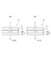
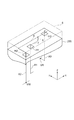
図1は、1つの記憶領域P(X,Y)の斜視図である。 FIG. 1 is a perspective view of one storage area P (X, Y).
個々の記憶領域P(X,Y)は、第1配線6と、第2配線7と、第1配線6の途中位置6aと第2配線7との間に配置され、且つ、第1配線6の途中位置6aと第2配線7に電気的に接続された磁気抵抗効果素子5と、スピン注入によって磁気抵抗効果素子5における感磁層の磁化の向きが変化するよう、磁気抵抗効果素子5に設けられたスピンフィルタFLとを備えている。
Each storage area P (X, Y) is disposed between the
第1配線6はX軸に沿って延びており、第2配線7もX軸に沿って延びている。各配線6,7の幅方向はY軸に平行であり、厚み方向はZ軸に平行である。
The
第1配線6の途中位置6aと第2配線7との間に電流を流すと、双方の配線6,7をそれぞれ囲むように磁界E6,E7が発生する。すなわち、磁界E6,E7はX軸を囲むように発生し、その向きは磁気抵抗効果素子5における感磁層の位置ではY軸に略平行となる。
When a current is passed between the
第1配線6の両端はそれぞれ端子VWと端子VRに接続され、第2配線7の一端は端子VCに接続され、他端は磁気抵抗効果素子5の下面に接続されている。第2配線7の一端と端子VCとの間にはスイッチ(電界効果トランジスタ)QRが介在している。
Both ends of the
情報の読み出し時には、情報の書き込み用端子VWを開放する。 When reading information, the information writing terminal VW is opened.
書き込み用端子VWを開放した状態で、端子VCの電位を読み出し用端子VRの電位に対して相対的に高くし、スイッチQRをONすると、第2配線7の端子VCから磁気抵抗効果素子5を介して第1配線6の読み出し用端子VRに情報読み出し電流IR1が流れ、互いに同一回転方向の磁界E6及び磁界E7が発生する。情報の読み出し時における磁界E6及び磁界E7は、X軸正方向に進む方向に共に右回りである。したがって、これらの配線間に位置する磁気抵抗効果素子5の位置における磁界E6,E7は互い相殺する。なお、磁界E6,E7は磁気ヨーク内を通っている。このような磁気ヨークは、第1及び/又は第2配線6,7の長手方向を囲み、感磁層2の厚み方向に垂直な方向の延長線上に位置する端部を有している。第1及び/又は第2配線6,7を電流が流れることによって、配線の周囲を囲むように発生した磁力線は、磁気ヨーク内を通り、その端部から感磁層内に導かれる。
When the potential of the terminal VC is made relatively high with respect to the potential of the read terminal VR while the write terminal VW is opened, and the switch QR is turned on, the
一方、書き込み用端子VWを開放した状態で、端子VCの電位を、読み出し用端子VRの電位に対して相対的に低くし、スイッチQRをONすると、第1配線6の読み出し用端子VRから磁気抵抗効果素子5を介して第2配線7の端子VCに情報読み出し電流IR2が流れ、互いに同一回転方向の磁界E6及び磁界E7が発生する。情報の読み出し時における磁界E6及び磁界E7は、X軸負方向に進む方向に共に右回りである。したがって、これらの配線間に位置する磁気抵抗効果素子5の位置における磁界E6,E7は互い相殺する。
On the other hand, when the write terminal VW is opened and the potential of the terminal VC is made relatively low with respect to the potential of the read terminal VR and the switch QR is turned on, the read terminal VR of the
このように、情報の読み出し時には、第1配線6及び第2配線7を流れる読み出し電流IR1,IR2の向きが同一であって、第1配線6及び第2配線7の周囲の磁界E6,E7が、磁気抵抗効果素子5の感磁層内において相殺されるように配置されている。情報読み出し時においては、双方の磁界E6,E7が相殺しているので、感磁層の磁化の向きを変更する力が弱くなり、したがって、ノイズの混入や読み出し電流の増加によっても感磁層の磁化反転が生じず、磁気メモリの信頼性を向上させることができる。
As described above, when reading information, the directions of the read currents I R1 and I R2 flowing through the
逆に、情報の書き込み時には、情報の読み出し用端子VRを開放する。読み出し用端子VRを開放した状態で、端子VCの電位を書き込み用端子VWの電位に対して相対的に高くし、スイッチQRをONすると、第2配線7の端子VCから磁気抵抗効果素子5を介して第1配線6の書き込み用端子VWに情報書き込み電流IW0が流れ、互いに逆回転方向の磁界E6及び磁界E7が発生する。このとき、情報の書き込み時における磁界E6はX軸負方向に進む方向に右回りであり、磁界E7はX軸正方向に進む方向に右回りである。したがって、これらの配線間に位置する磁気抵抗効果素子5には、Y軸負方向の向き磁界が作用する。
Conversely, when information is written, the information reading terminal VR is opened. When the read terminal VR is opened and the potential of the terminal VC is made relatively high with respect to the potential of the write terminal VW and the switch QR is turned on, the
一方、読み出し用端子VRを開放した状態で、端子VCの電位を、書き込み用端子VWの電位に対して相対的に低くし、スイッチQRをONすると、第1配線6の書き込み用端子VWから磁気抵抗効果素子5を介して第2配線7の端子VCに情報書き込み電流IW1が流れ、互いに逆回転方向の磁界E6及び磁界E7が発生する。このとき、情報の書き込み時における磁界E6はX軸正方向に進む方向に右回りであり、磁界E7はX軸負方向に進む方向に右回りである。したがって、これらの配線間に位置する磁気抵抗効果素子5には、Y軸正方向の向き磁界が作用する。
On the other hand, when the read terminal VR is opened, the potential of the terminal VC is relatively lowered with respect to the potential of the write terminal VW, and the switch QR is turned on, the magnetic force is applied from the write terminal VW of the
ここで、第1配線6及び第2配線7は、情報の書き込み時には、第1配線6及び第2配線7を流れる電流IW0、IW1の向きが逆向きであって、第1配線6及び第2配線7の周囲の磁界E6,E7の双方が、感磁層の磁化の向きをスピン注入によって変更する力(スピンランスファートルク)をアシストするように配置されている。特定の偏極したスピンは、スピンフィルタFLを透過又は反射して、感磁層内へ注入され、スピントランスファートルクを発生する。したがって、情報の書き込み時においては、スピン注入時の磁化の向きの変更力に加えて、第1配線6及び第2配線7を流れる電流に起因する磁界E6,E7のアシスト力によって、感磁層の磁化の向きが容易に変更される。
Here, when writing information, the
なお、スピン注入磁化反転を伴った磁気抵抗効果素子では、強磁性体を含む積層体の膜面に垂直な方向に電流を流すことにより強磁性体の磁化方向を反転させる。強磁性層と非磁性層との接合面においてアップスピン電子とダウンスピン電子の透過率の違いにより、スピン分極電流が流れる。強磁性層に流れ込んだスピン分極電流のスピン偏極電子は強磁性層の電子と交換相互作用をして電子間にトルクが発生し磁化反転が生じる。強磁性層の磁化反転の方向は、積層体に流す書き込み電流IW0,IW1の方向により決定される。したがって、電流の向きにより強磁性体の磁化方向の平行/反平行を制御でき、情報を記録することができる。 In the magnetoresistive effect element accompanied by the spin injection magnetization reversal, the magnetization direction of the ferromagnetic material is reversed by passing a current in a direction perpendicular to the film surface of the laminated body including the ferromagnetic material. A spin-polarized current flows due to the difference in transmittance between up-spin electrons and down-spin electrons at the interface between the ferromagnetic layer and the nonmagnetic layer. The spin-polarized electrons of the spin-polarized current that have flowed into the ferromagnetic layer interact with the electrons in the ferromagnetic layer to generate torque between the electrons, resulting in magnetization reversal. The direction of magnetization reversal of the ferromagnetic layer is determined by the direction of the write currents I W0 and I W1 that flow through the stack. Therefore, the parallel / antiparallel magnetization direction of the ferromagnetic material can be controlled by the direction of the current, and information can be recorded.
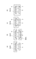
図2は、磁気抵抗効果素子5の縦断面図(磁化の向き平行時)(a)、磁気抵抗効果素子5の縦断面図(磁化の向き反平行時)(b)である。 FIG. 2 is a longitudinal sectional view of the magnetoresistive element 5 (when the magnetization direction is parallel) (a), and a longitudinal sectional view of the magnetoresistive element 5 (when the magnetization direction is antiparallel) (b).
磁気抵抗効果素子5は、トンネルバリア層を構成する絶縁層3を、感磁層2と固定層4とで挟んだ構造を有する。固定層4は、強磁性層4aと、磁化の向きを固定化させるために強磁性層4aに接合した反強磁性層4bとを備えており、磁気抵抗効果素子5はTMR素子を構成している。すなわち、磁気抵抗効果素子5は、感磁層2と(第1)固定層4との間に絶縁層3を備えたTMR素子である。TMR素子は、記憶された感磁層2の磁化の向きと固定層4の磁化の向きとの相違に応じて、読み出し時に絶縁層3をトンネルバリア層として通過する電子割合が異なる現象を利用した素子であり、高感度の記憶情報検出を行うことができる。
The
なお、図1に示したスピンフィルタFLは、固定層と非磁性層を接合してなり、この非磁性層は感磁層2に接合している。スピンフィルタFLを通過した電子は、TMR素子に導入されるため、感磁層2の磁化の向きと固定層4の磁化の向きの平行、反平行に応じて、情報の書き込み・読み出しを行うことができる。
The spin filter FL shown in FIG. 1 is formed by bonding a fixed layer and a nonmagnetic layer, and this nonmagnetic layer is bonded to the
メモリ情報の「1」、「0」は、TMR素子を構成する固定層4と感磁層2の磁化の向きの状態に応じて、すなわち、磁化の方向が平行であるか(図2(a))、反平行であるか(図2(b))に依存して規定される。固定層4と感磁層2の磁化の向きが反平行の時(図2(b))、磁化の向きが平行の時に比べて(図2(a))、厚み方向の電気抵抗Rの値が大きい。換言すれば、平行時の抵抗Rは閾値R0以下であり、反平行時の抵抗Rは閾値R0よりも大きくなる。したがって、「1」、「0」の情報の読出しは、TMR素子の厚み方向に電流IR(IR1又はIR2)を流し、MR(磁気抵抗)効果によるTMR素子の抵抗値又は電流値を測定することで行う。例えば、低抵抗の平行状態を「0」、高抵抗の反平行状態を「1」とする。
“1” and “0” of the memory information correspond to the state of magnetization directions of the fixed
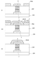
図3は、図1に示した磁気抵抗効果素子5を含む記憶部のIII−III矢印断面図である。
3 is a cross-sectional view taken along the line III-III of the storage unit including the
磁気抵抗効果素子5の周囲には、磁気ヨーク8が配置されている。磁気ヨーク8は、第1配線6の周囲に設けられた断面U字型の上部磁気ヨーク8Aと、第2配線7の周囲に設けられた断面U字型の下部磁気ヨーク8Bとからなり、それぞれの磁気ヨーク8A、8Bの開放端は対向している。なお、スピンフィルタの記載は省略している。
Around the
図3(a)に示すように、書き込み電流IW0を配線6,7に流した場合、磁界E6及びE7は、磁気抵抗効果素子5の感磁層2の位置において、略同一方向を向き、その強度を強め合う。
As shown in FIG. 3A, when a write current IW0 is applied to the
図3(b)に示すように、逆方向の書き込み電流IW1を配線6,7に流した場合、磁界E6及びE7は、磁気抵抗効果素子5の感磁層2の位置において、図3(a)とは逆向きの略同一方向を向き、その強度を強め合う。
As shown in FIG. 3B, when the write current I W1 in the reverse direction is passed through the
図3(c)に示すように、読み出し電流IR1を配線6,7に流した場合、磁界E6及びE7は、磁気抵抗効果素子5の感磁層2の位置において、互いに逆方向を向き、その強度を弱め合う。
As shown in FIG. 3C, when the read current I R1 is passed through the
図3(d)に示すように、読み出し電流IR2を配線6,7に流した場合、磁界E6及びE7は、磁気抵抗効果素子5の感磁層2の位置において、磁界の向きは図3(c)の場合とはそれぞれ逆ではあるが、互いに逆方向を向き、その強度を弱め合う。
As shown in FIG. 3 (d), in passing a read current I R2 to the
図1に示した磁界E6,E7について補足説明すると、第1配線6及び第2配線7を流れることによって発生する磁界E6,E7は、略同一平面(YZ平面)内において発生しているが、厳密には配線の長手方向(X軸)に沿ってずれている。すなわち、感磁層2内における磁界の相殺は、完全ではない。
When supplementarily explaining the magnetic fields E6 and E7 shown in FIG. 1, the magnetic fields E6 and E7 generated by flowing through the
本例では、個々の記憶領域P(X,Y)の記憶部は、磁気抵抗効果素子5を囲む磁気ヨーク8を備えているので、各配線6,7を流れることによって発生した各磁界E6,E7が磁気ヨーク8内に引き込まれ、感磁層2を含む磁気抵抗効果素子5に集中して磁界E6,E7を与えている。すなわち、情報の読み出し時における感磁層2内における磁界E6,E7が近接し、その相殺が効率的に行われている。また、上述の磁界アシストを用いたスピン注入型の磁気メモリにおいては、情報の書き込み時において、磁気ヨークを用いることにより、感磁層2内における磁界E6,E7を近接させ、合成磁界強度を増加させて、書き込み電流を著しく低減することができる。
In this example, the storage section of each storage area P (X, Y) includes the
磁界アシストがない場合のスピン注入磁化反転に要する書き込み電流の閾値は5×10⁷A/cm2であるが、磁界アシストをスピン注入と同時に用いた場合にはスピン注入磁化反転に要する書き込み電流の閾値は2.5×107A/cm2となり、さらに磁気ヨークを用いた場合には、スピン注入磁化反転に要する書き込み電流の閾値は5×106A/cm2となった。すなわち、磁気ヨークと磁界アシストを用いたスピン注入磁化反転型の磁気メモリの書き込み電流の大きさは、磁界アシストがない場合の書き込み電流の1/10、磁界アシストがあって磁気ヨークがない場合の書き込み電流の1/5に低減することができた。 The threshold of the write current required for the spin injection magnetization reversal without the magnetic field assist is 5 × 10 7 A / cm 2 , but when the magnetic field assist is used simultaneously with the spin injection, the write current required for the spin injection magnetization reversal is The threshold value was 2.5 × 10 7 A / cm 2 , and when a magnetic yoke was used, the write current threshold value required for spin injection magnetization reversal was 5 × 10 6 A / cm 2 . That is, the magnitude of the write current of the spin injection magnetization reversal type magnetic memory using the magnetic yoke and the magnetic field assist is 1/10 of the write current without the magnetic field assist, and there is no magnetic yoke with the magnetic field assist. It was possible to reduce to 1/5 of the write current.
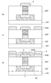
なお、磁気ヨークの構造には種々のものがある。 There are various magnetic yoke structures.
図4は、磁気ヨークの形状を変更した記憶分の縦断面図である。なお、スピンフィルタの記載は省略してある。 FIG. 4 is a longitudinal cross-sectional view of a stored portion in which the shape of the magnetic yoke is changed. The description of the spin filter is omitted.
図4(a)は、磁気ヨーク8が上部磁気ヨーク8Aのみからなるもの、図4(b)は上部磁気ヨーク8A及び下部磁気ヨーク8Bからなるもの、図4(c)は第1配線6の下面にまで回りこんだ上部磁気ヨーク8A’からなるもの、図4(d)は第2配線7の側部まで延びた上部磁気ヨーク8A”からなるものを示している。なお、上部及び下部なる用語は図面の上下に従うものであり、下部磁気ヨークのみを用いる場合は、上部磁気ヨークのみを用いる場合と同じである。
4A shows that the
図5は、磁気抵抗効果素子5を含む素子主要部の縦断面構成を示す図である。
FIG. 5 is a diagram showing a vertical cross-sectional configuration of the main part of the element including the
この素子主要部は、反強磁性層4b上に積層した強磁性層4a、絶縁層3、感磁層2からなるTMR素子と、TMR素子上に積層した非磁性導電層41及び固定層40からなるスピンフィルタFLとを備えている。固定層4、41の磁化の向きはY軸に平行である。
The main part of the element is composed of a TMR element composed of a
なお、上述の第1配線6及び第2配線7は、磁気抵抗効果素子5の位置において、固定層4の磁化の向き(Y軸)及び厚み方向(Z軸)の双方に垂直な方向(X軸)に延びている。第1配線6及び第2配線7の長手方向(X軸)を囲む方向は、感磁層2の位置において、固定層4の磁化の向きに一致するため、情報書き込み時に第1配線6及び第2配線7に通電を行った場合には、磁化の向きの変更を有効にアシストすることができる。
The
また、スピンフィルタFLは、感磁層2上に設けられた非磁性導電層41と、非磁性導電層41に接触した(第2)固定層40とを備え、この第2固定層40の磁化容易軸の向き(Y軸)は、(第1)固定層4の磁化容易軸の向き(Y軸)と平行である。したがって、感磁層2内に電子を注入する場合、特定の方向にスピンが偏極したスピン偏極電流が感磁層2内に注入され、感磁層2の電子との相互作用により磁化が反転する。
The spin filter FL includes a nonmagnetic
感磁層2の材料としては、例えばCo、CoFe、NiFe、NiFeCo、CoPt、CoFeBなどの強磁性材料を用いることができる。感磁層2は配線層より膜面に垂直に流れる電流により磁化方向を変化させることができ、感磁層2の面積が小さいほど磁化反転のために必要な電流(電流の閾値)を小さくすることができる。感磁層2の面積は0.01μm2以下が好ましい。感磁層2の面積が0.01μm2を超えると、磁化反転に必要な閾値電流値が増大するために、情報の記録が困難になる。さらに感磁層2は厚みが小さいほど磁化反転のための電流の閾値を小さくすることができる。感磁層2の厚みは0.01μm以下が好ましい。厚みが0.01μmを超えると磁化反転に必要な電流値が増大し、情報の記録が困難になる。
As the material of the
非磁性絶縁層3の材料としては、Al、Zn、Mgといった金属の酸化物または窒化物、例えばAl2O3やMgOが好適である。固定層4、40の構造としては、反強磁性層を強磁性材料層に付与した交換結合型を用いることができる。また、反強磁性体の材料としては、IrMn、PtMn、FeMn、NiMn、PtPdMn、RuMn、NiO、またはこれらのうち任意の組み合わせの材料を用いることができる。非磁性層41の材料としては、CuやRuを用いることができる。各種配線材料としては、Cu、AuCu、W、Al等を用いることができる。非磁性導電層41の材料としては、例えばCuを用いることができる。
As a material of the nonmagnetic insulating
図6は、上記記憶領域Pを複数備えた磁気メモリの回路図である。 FIG. 6 is a circuit diagram of a magnetic memory having a plurality of the storage areas P.
この磁気メモリは、スイッチQRの導通を制御するゲートに接続されたワード線WLを備えており、ワード線WLの電位はスイッチング回路SWCによって決定される。また、読み出し用端子VRは第1ビット線BL1、書き込み用端子VWは第2ビット線BL2、端子VCは第3ビット線BL3に接続され、これらのビット線BL1,BL2,BL3の電位は制御回路CONTによって制御される。 This magnetic memory includes a word line WL connected to a gate that controls conduction of the switch QR, and the potential of the word line WL is determined by the switching circuit SWC. The read terminal VR is connected to the first bit line BL1, the write terminal VW is connected to the second bit line BL2, and the terminal VC is connected to the third bit line BL3. The potentials of these bit lines BL1, BL2, and BL3 are controlled by a control circuit. Controlled by CONT.
なお、特定のアドレスの記憶領域P(X,Y)に情報を書き込む場合(例えば「1」)、該当するY列目の記憶領域の読み出し用端子VRを開放し、書き込み用端子VWの電位を共通端子VCに対して相対的に増加させ、スイッチング回路SWCがワード線WLの電位を制御してX行目のスイッチQRをONする。これにより、磁気抵抗効果素子5の感磁層の磁化の向きが固定層の磁化の向きに対して、例えば、「反平行」となり、「1」が書き込まれる。
When information is written into the storage area P (X, Y) at a specific address (eg, “1”), the read terminal VR of the corresponding Y-th storage area is opened, and the potential of the write terminal VW is set to be the same. The switching circuit SWC controls the potential of the word line WL to turn on the switch QR in the X-th row. As a result, the magnetization direction of the magnetosensitive layer of the
「0」と書き込む場合には、これらの磁化の向きを、例えば、「平行」とする。すなわち、特定のアドレスの記憶領域P(X,Y)に情報を書き込む場合(例えば「0」)、該当するY列目の記憶領域の読み出し用端子VRを開放し、書き込み用端子VWの電位を共通端子VCに対して相対的に減少させ、スイッチング回路SWCがワード線WLの電位を制御してX行目のスイッチQRをONする。これにより、例えば、「0」が書き込まれる。 In the case of writing “0”, the direction of the magnetization is, for example, “parallel”. That is, when information is written to the storage area P (X, Y) at a specific address (for example, “0”), the read terminal VR of the corresponding Y-th storage area is opened, and the potential of the write terminal VW is set. The switching circuit SWC controls the potential of the word line WL to turn on the switch QR in the X-th row. Thereby, for example, “0” is written.
特定のアドレスの記憶領域P(X,Y)の情報を読み出す場合、該当するY列目の記憶領域の書き込み用端子VWを開放し、読み出し用端子VRの電位を共通端子VCに対して相対的に増加させ、スイッチング回路SWCがワード線WLの電位を制御してX行目のスイッチQRをONする。これにより、記憶領域P(X,Y)に位置する磁気抵抗効果素子5に書き込まれた情報「1」「0」に応じた電流が、読み出し用端子VRと共通端子VCとの間を流れ、これに基づき記憶情報を判別することができる。なお、読み出し時の電流の向きは、これとは逆であってもよく、設計に応じて適宜設定すればよい。
When reading the information in the storage area P (X, Y) of a specific address, the write terminal VW of the corresponding Y-th storage area is opened, and the potential of the read terminal VR is relative to the common terminal VC. The switching circuit SWC controls the potential of the word line WL to turn on the switch QR in the Xth row. Thereby, a current corresponding to the information “1” and “0” written in the
なお、スイッチング回路SWC及び制御回路CONTは、半導体基板内に形成される。 Note that the switching circuit SWC and the control circuit CONT are formed in the semiconductor substrate.
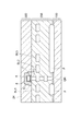
図7は、図6に示した磁気メモリのVII−VII矢印縦断面図である。 7 is a vertical cross-sectional view of the magnetic memory shown in FIG. 6 taken along the line VII-VII.
読み出し配線7を構成する下部電極は、半導体基板100上に形成された絶縁層200を厚み方向に貫通する垂直配線A1を介して、読み出しトランジスタQRのソース又はドレイン電極34aに接続されている。ここでは、ドレイン電極34aとする。読み出しトランジスタQRのゲート電極34gは、ワード線WL自体を構成する又はワード線WLに接続されている。読み出しトランジスタQRは、ドレイン電極34a,ソース電極34bと、ゲート電極34gと、ドレイン電極34a,ソース電極34b直下に形成されたドレイン領域34a’,ソース領域34b’からなり、ゲート電極34gの電位に応じてドレイン電極34a,ソース電極34bは接続される。ソース電極34bは、内部接続配線15を介してビット線BL3に接続されている。
The lower electrode constituting the
図8は、図6に示した磁気メモリのVIII−VIII矢印縦断面図である。 8 is a vertical cross-sectional view of the magnetic memory shown in FIG. 6 taken along line VIII-VIII.
読み出しトランジスタQRの周囲には、LOCOS(local oxidation of silicon)による酸化膜(SiO2)Fが形成されている。 An oxide film (SiO 2 ) F made of LOCOS (local oxidation of silicon) is formed around the read transistor QR.
また、ビット線BL1、BL2,BL3やワード線WLは、半導体基板100上に形成された下部絶縁層200内に埋設されており、下部絶縁層200上には上部絶縁層24が成されている。また、下部絶縁層200内には必要に応じて複数の配線が設けられる。垂直配線A1は、半導体基板100の表面から下部絶縁層200を貫通する配線である。半導体基板100は例えばSiからなり、ソース領域及びドレイン領域には半導体基板100とは異なる導電型の不純物が添加されている。下部絶縁層200はSiO2等からなる。
The bit lines BL 1,
なお、上述の磁気ヨーク8は、磁気抵抗効果素子5の側方の周囲を全て覆う密閉型としてもよい。なお、有効磁界の感磁層への集中を行う観点からは、密閉型ではなく、上述のように、配線の前後方向が開放している磁気ヨークの方が好ましい。
The
図9は、密閉型の磁気ヨーク8を備えた記憶部の斜視図である。
FIG. 9 is a perspective view of the storage unit including the sealed
下部絶縁層200上に、第2配線7、磁気抵抗効果素子5、第1配線6を順次積層した後、これを覆う絶縁被覆を形成し、この上に磁気ヨーク8を形成する。磁気ヨーク8の側壁は、磁気抵抗効果素子5のZ軸の周囲の全てにおいて連続しており、磁気ヨーク8の頂壁は側壁の頂面に設けられ、磁気抵抗効果素子5を封止している。
The
下部絶縁層200には、半導体基板100に到達するスルーホールH1,H2,H3が設けられている。水平方向(XY平面内)に延びた第2配線7の一端は垂直配線A1に接続され、垂直配線A1はスルーホールH1を介して半導体基板100内の素子(トランジスタQR)に接続されている。水平方向に延びた第1配線6の一端は、垂直配線A2に接続され、垂直配線A2はスルーホールH2を介して半導体基板100内の素子(端子VW)に接続されている。水平方向に延びた第1配線6の他端は、垂直配線A3に接続され、垂直配線A3はスルーホールH3を介して半導体基板100内の素子(端子VR)に接続されている。
The lower
上述の密閉型の磁気ヨーク8を用いた場合、磁気抵抗効果素子5の外部からの漏れ磁束やノイズが、側方のいずれの方向から伝播してきても、磁気ヨーク8によって全てシールドされるため、信頼性に優れるという効果がある。
When the above-described sealed
このように、上述の磁気メモリは、磁気抵抗効果素子を高密度化しても、書き込み電流の増加が抑制でき、また、隣接する磁気抵抗効果素子に影響を与えず、また、アシスト磁界をスピン注入と共に用いるため、高速のアクセス速度を得ることができる。 As described above, the above-mentioned magnetic memory can suppress an increase in write current even if the magnetoresistive effect element is increased in density, does not affect the adjacent magnetoresistive effect element, and spin-injects an assist magnetic field. Therefore, a high access speed can be obtained.
図10は、図1に示した磁気メモリにおける読み出し電流IR及び書き込み電流IW0、IW1の値と磁気抵抗効果素子5の抵抗値との関係を示すグラフである。 Figure 10 is a graph showing the relationship between the resistance value of the read current I R and a write current I W0, the value and the magnetoresistive element 5 I W1 in the magnetic memory shown in FIG.
情報記録時の書き込み電流IW1,IW0の絶対値は1mA前後であり、情報読み出し時の読み出し電流IRの絶対値は0.4mA前後である。正の書き込み電流IW1の絶対値が0.8mAを超えると、感磁層の磁化反転が生じて反平行状態「1」が記録され、負の書き込み電流IW0の絶対値が0.8mAを超えると、感磁層の磁化反転が生じて平行状態「0」が記録される。 The absolute value of the information recording time of the write current I W1, I W0 is around 1 mA, the absolute value of the read current I R at information reading is around 0.4 mA. When the absolute value of the positive write current I W1 exceeds 0.8 mA, magnetization reversal of the magnetosensitive layer occurs and the antiparallel state “1” is recorded, and the absolute value of the negative write current I W0 becomes 0.8 mA. If exceeded, magnetization reversal of the magnetosensitive layer occurs and a parallel state “0” is recorded.
すなわち、強磁性層(磁化固定層)/非磁性層/強磁性層の積層体において、積層体の正方向に電流を増やしてゆくと所定の閾値(臨界電流)で強磁性層の磁化方向が反転し、磁化固定層と強磁性層との磁化方向が反平行(=「1」)となり磁気抵抗効果素子の抵抗値が増大する。その後、電流値を負の方向に減少させてゆくと、負の所定の閾値(臨界電流)で強磁性層の磁化が反転し、磁化固定層と強磁性層との磁化方向が平行(=「0」)となり磁気抵抗効果素子5の抵抗値が減少する。なお、これらの情報の記録ができる電流値は、消費電力や外部へのノイズの影響も考慮して1.5mA以下に設定してある。
That is, in a ferromagnetic layer (magnetization pinned layer) / nonmagnetic layer / ferromagnetic layer laminate, when the current is increased in the positive direction of the laminate, the magnetization direction of the ferromagnetic layer is changed at a predetermined threshold (critical current). The magnetization direction of the magnetization fixed layer and the ferromagnetic layer becomes antiparallel (= “1”) and the resistance value of the magnetoresistive effect element increases. Thereafter, when the current value is decreased in the negative direction, the magnetization of the ferromagnetic layer is reversed at a predetermined negative threshold (critical current), and the magnetization directions of the magnetization fixed layer and the ferromagnetic layer are parallel (= “ 0 ") and the resistance value of the
なお、スピン注入磁化反転を伴った記録素子では、臨界電流値を超えない電流を流した場合は、強磁性体の磁化方向は変化することはないため、読出しのための電流を臨界電流値以下にすることにより、記録した情報を書き換えることなく、非破壊による読み出しを行うことができる。 In a recording element with spin injection magnetization reversal, when a current that does not exceed the critical current value is passed, the magnetization direction of the ferromagnet does not change, so the current for reading is less than the critical current value. By doing so, it is possible to perform non-destructive reading without rewriting the recorded information.
また、膜面に垂直に流れる電流により感磁層の磁化反転を行うことにより、データに記録を行うスピン注入記録においては、反転のための電流は1×10⁸〜1×10⁶A/cm2と大きく、また、TMR素子の抵抗は比較的高い。したがって、書込み電流を流した場合、TMR素子部の発熱が大きくなる傾向があるが、上述の磁気メモリでは、配線に磁気ヨーク8を設けているので、配線を流れる電流によって生じる電流磁界を効率的に感磁層に印加し、より少ない電流でスピン注入磁化反転を行わせている。さらに、磁気ヨーク8により外部磁界による外部磁界によるデータを記録した感磁層への影響を低減でき、メモリデバイスの外部磁界耐性を改善することができる。
In spin injection recording in which data is recorded by performing magnetization reversal of the magnetosensitive layer by current flowing perpendicularly to the film surface, the current for reversal is 1 × 10 8 to 1 × 10 6 A / cm. 2 and the resistance of the TMR element is relatively high. Therefore, when a write current is passed, heat generation in the TMR element portion tends to increase. However, in the above-described magnetic memory, since the
次に、上述の磁気メモリの製造方法について説明する。ここでは、(図4(a))の構造の磁気メモリについて説明する。 Next, a method for manufacturing the above magnetic memory will be described. Here, a magnetic memory having the structure shown in FIG. 4A will be described.
まず、図11(a)に示すように、下部絶縁層200上に中央部が開口したホトレジストPR1をパターニングする。次に、図11(b)に示すように、スパッタ法などでホトレジストPR1上に電極層7を堆積する。さらに、図11(c)に示すように、リフトオフを行い、ホトレジストPR1上の電極材料を除去する。しかる後、図11(d)に示すように、下部絶縁層200上にタンタルからなる下地層201、IrMnからなる反強磁性層4b、CoFeからなる強磁性層4a、Al2O3からなる絶縁層3、CoFeからなる感磁層2、Ruからなる非磁性導電層41、CoFeからなる強磁性層40、タンタルからなるキャップ層202を順次堆積する。なお、絶縁層3は、Alの堆積後にこれを酸化することで形成することもできる。堆積にはスパッタ法を用いることができる。次に、図11(e)に示すように、キャップ層202の中央部上にホトレジストPR2をパターニングする。すなわち、ホトレジストPR2は下部配線7の上方に位置する。
First, as shown in FIG. 11A, a photoresist PR1 having an opening at the center is patterned on the lower insulating
しかる後、図12(f)に示すように、ホトレジストPR2をマスクとして、積層体のドライエッチングを行う。このエッチングは下部配線7の表面が露出するまで行う。次に、図12(g)に示すように、ホトレジストPR2を除去した後、下部絶縁層200上にSiO2からなる中間絶縁層200’をスパッタ法やCVD法などでキャップ層202が中間絶縁層200’内に埋め込まれるまで堆積する。そして、図12(h)に示すように、キャップ層202の表面が露出するまで、CMP(Chemical Mechanical Polish)装置を用いて中間絶縁層200’を研磨し、中間絶縁層200’の表面を平滑化する。
Thereafter, as shown in FIG. 12F, the stacked body is dry-etched using the photoresist PR2 as a mask. This etching is performed until the surface of the
次に、図13(i)に示すように、中間絶縁層200’の表面上に中央部が開口したホトレジストPR3をパターニングする。しかる後、ホトレジストPR3上にスパッタ法などで配線材料6を堆積し(図13(j))、ホトレジストPR3のリフトオフを行い、キャップ層202上に上部配線6を形成する(図13(k))。配線構造としては、Ti,Cu,Taなどの材料の1種からなる単層構造あるいは複数種からなる多層構造などを用いることができる。
Next, as shown in FIG. 13I, a photoresist PR3 having an opening at the center is patterned on the surface of the intermediate insulating layer 200 '. Thereafter, a
更に、中間絶縁層200’上に上部配線6の形成領域を含む領域が開口したホトレジストPR4をパターニングする(図14(l))。次に、ホトレジストPR4上にスパッタ法などでNeFeなどの磁性材料8を堆積する(図14(m))。次に、リフトオフを行い、余分な磁性材料をホトレジストPR4と共に除去し、上部磁気ヨーク8A(8)を形成する(図14(n))。最後に、図15に示すように、CVD装置を用いてSiO2からなる上部絶縁層24を磁気ヨーク8上に堆積する。
Further, a photoresist PR4 having an opening including a region where the
次に、下部磁気ヨークも備えた磁気メモリの製造方法について説明する。ここでは、(図4(b))の構造の磁気メモリについて説明する。 Next, a method for manufacturing a magnetic memory having a lower magnetic yoke will be described. Here, a magnetic memory having the structure shown in FIG. 4B will be described.
まず、図16(a)に示すように、下部絶縁層200上に中央部が大きく開口したホトレジストPR1をパターニングする。次に、図16(b)に示すように、スパッタ法などでホトレジストPR1上にNiFeなどの磁性材料8B(8)を堆積する。このホトレジストPR1をリフトオフして中央に磁性材料を残し、さらに、磁性材料8Bの周辺部が開口したホトレジストPR2を基板上にパターニングする(図16(c))。
First, as shown in FIG. 16A, a photoresist PR1 having a large opening at the center is patterned on the lower insulating
次に、図16(d)に示すように、スパッタ法などでホトレジストPR1上にNiFeなどの磁性材料を更に堆積し、続いて、リフトオフを行う(図16(e))。これにより、断面がU字形の下部磁気ヨー8Bが完成する。しかる後、下部磁気ヨーク8Bの凹部内が露出する開口を有するホトレジストPR3をパターニングする(図16(f))。
Next, as shown in FIG. 16D, a magnetic material such as NiFe is further deposited on the photoresist PR1 by sputtering or the like, and then lift-off is performed (FIG. 16E). Thereby, the lower
次に、図17(g)に示すように、スパッタ法などでホトレジストPR3上に電極層7を堆積する。さらに、図17(b)に示すように、リフトオフを行い、ホトレジストPR3上の電極材料を除去する。しかる後、図17(h)に示すように、下部絶縁層200上にCVD法やスパッタ法を用いてSiO2からなる第1中間絶縁層200’を堆積する。なお、CVD法におけるSiO2の原料は例えばSi(OC2H5)4である。次に、図17(i)に示すように、CMP(Chemical Mechanical Polish)装置を用いて第1中間絶縁層200’を研磨し、第1中間絶縁層200’の表面を平滑化する。
Next, as shown in FIG. 17G, an
次に、図17(j)に示すように、第1中間絶縁層200’の表面上にタンタルからなる下地層201、IrMnからなる反強磁性層4b、CoFeからなる強磁性層4a、Al2O3からなる絶縁層3、CoFeからなる感磁層2、Ruからなる非磁性導電層41、CoFeからなる強磁性層40、タンタルからなるキャップ層202を順次堆積する。なお、絶縁層3は、Alの堆積後にこれを酸化することで形成することもできる。堆積にはスパッタ法を用いることができる。
Next, as shown in FIG. 17 (j), the
次に、図18(k)に示すように、キャップ層202の中央部上にホトレジストPR4をパターニングする。すなわち、ホトレジストPR4は下部配線7の上方に位置する。
Next, as shown in FIG. 18K, a photoresist PR4 is patterned on the central portion of the
しかる後、図18(l)に示すように、ホトレジストPR4をマスクとして、積層体のドライエッチングを行う。このエッチングは下部配線7の表面が露出するまで行う。次に、図18(m)に示すように、ホトレジストPR4を除去した後、第1中間絶縁層200’上にSiO2からなる第2中間絶縁層200”を、スパッタ法やCVD法などでキャップ層202が第2中間絶縁層200”内に埋め込まれるまで堆積する。そして、図19(n)に示すように、キャップ層202の表面が露出するまで、CMP装置を用いて第2中間絶縁層200”を研磨し、第2中間絶縁層200”の表面を平滑化する。
Thereafter, as shown in FIG. 18L, the stacked body is dry-etched using the photoresist PR4 as a mask. This etching is performed until the surface of the
次に、図19(o)に示すように、第2中間絶縁層200”の表面上に中央部が開口したホトレジストPR5をパターニングする。しかる後、ホトレジストPR5上にスパッタ法などで配線材料6を堆積し(図19(p))、ホトレジストPR5のリフトオフを行い、キャップ層202上に上部配線6を形成する(図20(q))。配線構造としては、Ti,Cu,Taなどの材料の1種からなる単層構造あるいは複数種からなる多層構造などを用いることができる。
Next, as shown in FIG. 19 (o), a photoresist PR5 having an opening at the center is patterned on the surface of the second intermediate insulating
更に、第2中間絶縁層200”上に上部配線6の形成領域を含む領域が開口したホトレジストPR6をパターニングする(図20(r))。次に、ホトレジストPR6上にスパッタ法などでNeFeなどの磁性材料8を堆積する(図20(s))。次に、リフトオフを行い、余分な磁性材料をホトレジストPR6と共に除去し、上部磁気ヨーク8A(8)を形成する(図21(t))。最後に、図21(u)に示すように、CVD装置を用いてSiO2からなる上部絶縁層24を磁気ヨーク8上に堆積する。
Further, a photoresist PR6 having an opening including a region where the
なお、密閉型の磁気ヨークも備えた磁気メモリの製造方法について説明する。ここでは、図9の構造の磁気メモリについて説明する。 A method of manufacturing a magnetic memory that also includes a sealed magnetic yoke will be described. Here, the magnetic memory having the structure of FIG. 9 will be described.
下部配線7は下部絶縁層200のスルーホールを介して半導体基板の素子に接続しておき、図11(a)から図13(k)までの工程を実行する。
The
しかる後、図22に示すように、上部配線6をマスクとして周囲の絶縁層200’を下部絶縁層200の表面が露出するまでドライエッチングし、露出した素子及び基板表面上を保護絶縁膜200iで被覆する(図22(l))。しかる後、下部絶縁層200上に素子形成領域を含む領域が開口したホトレジストPRをパターニングし(図22(m)、続いて、この上にNiFeなどの磁気材料を堆積し、リフトオフを行って密閉型の磁気ヨーク8が完成する(図22(n))。
Thereafter, as shown in FIG. 22, the surrounding insulating
本発明は、磁気メモリに利用することができる。 The present invention can be used for a magnetic memory.
2・・・感磁層、3・・・非磁性絶縁層、4・・・固定層、5・・・磁気抵抗効果素子、6・・・上部配線、6a・・・途中位置、7・・・下部配線、8・・・磁気ヨーク、24・・・上部絶縁層、41・・・非磁性導電層、100・・・半導体基板、200・・・下部絶縁層、201・・・下地層、202・・・キャップ層、A1・・・垂直配線、A2・・・垂直配線、BL1,BL2,BL3・・・ビット線、CONT・・・制御回路、FL・・・スピンフィルタ、H1,H2,H3・・・スルーホール、P・・・記憶領域、QR・・・トランジスタ、SWC・・・スイッチング回路、VC・・・共通端子、VR・・・端子、WL・・・ワード線。
2 ... magnetic sensitive layer, 3 ... nonmagnetic insulating layer, 4 ... fixed layer, 5 ... magnetoresistive element, 6 ... upper wiring, 6a ... halfway position, 7 Lower wiring, 8 ... magnetic yoke, 24 ... upper insulating layer, 41 ... nonmagnetic conductive layer, 100 ... semiconductor substrate, 200 ... lower insulating layer, 201 ... underlayer, 202 ... cap layer, A1 ... vertical wiring, A2 ... vertical wiring, BL1, BL2, BL3 ... bit line, CONT ... control circuit, FL ... spin filter, H1, H2, H3... Through hole, P... Storage area, QR... Transistor, SWC... Switching circuit, VC .. Common terminal, VR.
Claims (4)
個々の前記記憶領域は、
第1配線と、
第2配線と、
前記第1配線と前記第2配線との間に配置され、且つ、前記第1配線と前記第2配線に電気的に接続された磁気抵抗効果素子と、
スピン注入によって前記磁気抵抗効果素子における感磁層の磁化の向きが変化するよう、前記磁気抵抗効果素子に設けられたスピンフィルタと、
前記第1及び第2配線を流れる電流によって発生する磁界を前記感磁層内に導くように前記磁気抵抗効果素子を囲む磁気ヨークと、
を備えていることを特徴とする磁気メモリ。 In a magnetic memory formed by arranging a plurality of storage areas,
Each said storage area is
A first wiring;
A second wiring;
A magnetoresistive effect element disposed between the first wiring and the second wiring and electrically connected to the first wiring and the second wiring;
A spin filter provided in the magnetoresistive element so that the magnetization direction of the magnetosensitive layer in the magnetoresistive element is changed by spin injection;
A magnetic yoke surrounding the magnetoresistive element so as to guide a magnetic field generated by a current flowing through the first and second wires into the magnetosensitive layer;
A magnetic memory comprising:
前記感磁層上に設けられた非磁性導電層と、
前記非磁性導電層に接触した第2固定層と、
を備え、
この第2固定層の磁化の向きは、前記第1固定層の磁化の向きと平行であることを特徴とする請求項1又は2に記載の磁気メモリ。 The spin filter is
A nonmagnetic conductive layer provided on the magnetosensitive layer;
A second pinned layer in contact with the nonmagnetic conductive layer;
With
3. The magnetic memory according to claim 1, wherein the magnetization direction of the second pinned layer is parallel to the magnetization direction of the first pinned layer.
個々の前記記憶領域は、
第1配線と、
第2配線と、
前記第1配線と前記第2配線との間に配置され、且つ、前記第1配線と前記第2配線に電気的に接続された磁気抵抗効果素子と、
スピン注入によって前記磁気抵抗効果素子における感磁層の磁化の向きが変化するよう、前記磁気抵抗効果素子に設けられたスピンフィルタと、
前記第1及び/又は第2配線の長手方向を囲み、前記感磁層の厚み方向に垂直な方向の延長線上に位置する端部を有する磁気メモリと、
を備えていることを特徴とする磁気メモリ。 In a magnetic memory formed by arranging a plurality of storage areas,
Each said storage area is
A first wiring;
A second wiring;
A magnetoresistive effect element disposed between the first wiring and the second wiring and electrically connected to the first wiring and the second wiring;
A spin filter provided in the magnetoresistive element so that the magnetization direction of the magnetosensitive layer in the magnetoresistive element is changed by spin injection;
A magnetic memory having an end portion that surrounds a longitudinal direction of the first and / or second wiring and is located on an extension line in a direction perpendicular to a thickness direction of the magnetosensitive layer;
A magnetic memory comprising:
Priority Applications (1)
| Application Number | Priority Date | Filing Date | Title |
|---|---|---|---|
| JP2005370440A JP2007173597A (en) | 2005-12-22 | 2005-12-22 | Magnetic memory |
Applications Claiming Priority (1)
| Application Number | Priority Date | Filing Date | Title |
|---|---|---|---|
| JP2005370440A JP2007173597A (en) | 2005-12-22 | 2005-12-22 | Magnetic memory |
Publications (1)
| Publication Number | Publication Date |
|---|---|
| JP2007173597A true JP2007173597A (en) | 2007-07-05 |
Family
ID=38299729
Family Applications (1)
| Application Number | Title | Priority Date | Filing Date |
|---|---|---|---|
| JP2005370440A Pending JP2007173597A (en) | 2005-12-22 | 2005-12-22 | Magnetic memory |
Country Status (1)
| Country | Link |
|---|---|
| JP (1) | JP2007173597A (en) |
Cited By (11)
| Publication number | Priority date | Publication date | Assignee | Title |
|---|---|---|---|---|
| WO2009011216A1 (en) * | 2007-07-19 | 2009-01-22 | Sony Corporation | Storage element and memory |
| JP2010010683A (en) * | 2008-06-24 | 2010-01-14 | Samsung Electronics Co Ltd | Information storage device and method of operating the same |
| CN102403038A (en) * | 2010-09-06 | 2012-04-04 | 索尼公司 | Memory element and memory device |
| CN102403028A (en) * | 2010-09-13 | 2012-04-04 | 索尼公司 | Storage element and memory device |
| CN102403026A (en) * | 2010-09-07 | 2012-04-04 | 索尼公司 | Memory element and memory device |
| CN102403029A (en) * | 2010-09-14 | 2012-04-04 | 索尼公司 | Memory element and memory device |
| CN102592658A (en) * | 2011-01-07 | 2012-07-18 | 索尼公司 | Storage element and storage device |
| CN102610270A (en) * | 2011-01-18 | 2012-07-25 | 索尼公司 | Storage element and memory device |
| JP2012528422A (en) * | 2009-05-29 | 2012-11-12 | クアルコム,インコーポレイテッド | Spin transfer torque-magnetic tunnel junction device and method of operation |
| CN102403028B (en) * | 2010-09-13 | 2016-12-14 | 索尼公司 | Memory element and storage device |
| KR101906708B1 (en) | 2017-01-23 | 2018-10-10 | 고려대학교 산학협력단 | Asymmetric magnetic devices |
Citations (3)
| Publication number | Priority date | Publication date | Assignee | Title |
|---|---|---|---|---|
| JP2005150482A (en) * | 2003-11-18 | 2005-06-09 | Sony Corp | Magnetoresistance effect element and magnetic memory device |
| JP2007123637A (en) * | 2005-10-28 | 2007-05-17 | Toshiba Corp | Spin injection magnetic random access memory |
| JP2007150205A (en) * | 2005-11-30 | 2007-06-14 | Tdk Corp | Magnetic memory |
-
2005
- 2005-12-22 JP JP2005370440A patent/JP2007173597A/en active Pending
Patent Citations (3)
| Publication number | Priority date | Publication date | Assignee | Title |
|---|---|---|---|---|
| JP2005150482A (en) * | 2003-11-18 | 2005-06-09 | Sony Corp | Magnetoresistance effect element and magnetic memory device |
| JP2007123637A (en) * | 2005-10-28 | 2007-05-17 | Toshiba Corp | Spin injection magnetic random access memory |
| JP2007150205A (en) * | 2005-11-30 | 2007-06-14 | Tdk Corp | Magnetic memory |
Cited By (18)
| Publication number | Priority date | Publication date | Assignee | Title |
|---|---|---|---|---|
| TWI397069B (en) * | 2007-07-19 | 2013-05-21 | Sony Corp | Memory components and memory |
| JP2009026944A (en) * | 2007-07-19 | 2009-02-05 | Sony Corp | Storage element and memory |
| WO2009011216A1 (en) * | 2007-07-19 | 2009-01-22 | Sony Corporation | Storage element and memory |
| US8339840B2 (en) | 2007-07-19 | 2012-12-25 | Sony Corporation | Storage element and memory |
| JP2010010683A (en) * | 2008-06-24 | 2010-01-14 | Samsung Electronics Co Ltd | Information storage device and method of operating the same |
| JP2012528422A (en) * | 2009-05-29 | 2012-11-12 | クアルコム,インコーポレイテッド | Spin transfer torque-magnetic tunnel junction device and method of operation |
| CN102403038A (en) * | 2010-09-06 | 2012-04-04 | 索尼公司 | Memory element and memory device |
| CN102403038B (en) * | 2010-09-06 | 2016-08-24 | 索尼公司 | Memory element and memory device |
| CN102403026A (en) * | 2010-09-07 | 2012-04-04 | 索尼公司 | Memory element and memory device |
| CN102403028A (en) * | 2010-09-13 | 2012-04-04 | 索尼公司 | Storage element and memory device |
| CN102403028B (en) * | 2010-09-13 | 2016-12-14 | 索尼公司 | Memory element and storage device |
| CN102403029B (en) * | 2010-09-14 | 2016-05-25 | 索尼公司 | Memory element and storage device |
| CN102403029A (en) * | 2010-09-14 | 2012-04-04 | 索尼公司 | Memory element and memory device |
| CN102592658A (en) * | 2011-01-07 | 2012-07-18 | 索尼公司 | Storage element and storage device |
| CN102592658B (en) * | 2011-01-07 | 2016-08-24 | 索尼公司 | Memory element and storage device |
| CN102610270A (en) * | 2011-01-18 | 2012-07-25 | 索尼公司 | Storage element and memory device |
| CN102610270B (en) * | 2011-01-18 | 2016-08-03 | 索尼公司 | Memory element and storage arrangement |
| KR101906708B1 (en) | 2017-01-23 | 2018-10-10 | 고려대학교 산학협력단 | Asymmetric magnetic devices |
Similar Documents
| Publication | Publication Date | Title |
|---|---|---|
| JP4779608B2 (en) | Magnetic memory | |
| JP4384183B2 (en) | Magnetoresistive element and magnetic memory | |
| JP5470602B2 (en) | Magnetic storage | |
| JP5460606B2 (en) | Spin injection MRAM device with separate CPP assisted writing | |
| JP5062481B2 (en) | Magnetic memory cell, magnetic random access memory, and data read / write method to magnetic random access memory | |
| TWI622158B (en) | Storage element, storage device, method of manufacturing storage element, and magnetic head | |
| JP5201539B2 (en) | Magnetic random access memory | |
| JP2007173597A (en) | Magnetic memory | |
| JP2006114868A (en) | Magnetic recording element and magnetic recording device using the same | |
| JP2007273493A (en) | Magnetic memory device and its manufacturing method | |
| JP2011210830A (en) | Magnetic storage element and magnetic storage apparatus | |
| JPWO2007119446A1 (en) | MRAM and data read / write method of MRAM | |
| JP2004153181A (en) | Magnetoresistance effect element and magnetic memory | |
| JP2013115400A (en) | Storage element, storage device | |
| CN111226312A (en) | Tunnel magnetoresistance effect element, magnetic memory and built-in memory | |
| JP2004303837A (en) | Magnetic storage cell, magnetic memory device, and its manufacturing method | |
| JP2004087870A (en) | Magnetoresistive effect element and magnetic memory device | |
| US20060266470A1 (en) | Magnetic memory and method of manufacturing same | |
| JP5058206B2 (en) | Method for manufacturing magnetoresistive element | |
| JP4876572B2 (en) | Magnetic memory | |
| JP2011253884A (en) | Magnetic memory device | |
| US6992921B2 (en) | Magnetic random access memory and data write method for the same | |
| JP2006108316A (en) | Memory element and memory | |
| JP2008218736A (en) | Magnetic memory device | |
| JP5441024B2 (en) | Magnetic storage |
Legal Events
| Date | Code | Title | Description |
|---|---|---|---|
| A621 | Written request for application examination |
Free format text: JAPANESE INTERMEDIATE CODE: A621 Effective date: 20080925 |
|
| A977 | Report on retrieval |
Free format text: JAPANESE INTERMEDIATE CODE: A971007 Effective date: 20110407 |
|
| A131 | Notification of reasons for refusal |
Free format text: JAPANESE INTERMEDIATE CODE: A131 Effective date: 20110510 |
|
| A02 | Decision of refusal |
Free format text: JAPANESE INTERMEDIATE CODE: A02 Effective date: 20110920 |