JP2007123802A - Electronic component - Google Patents
Electronic component Download PDFInfo
- Publication number
- JP2007123802A JP2007123802A JP2006082227A JP2006082227A JP2007123802A JP 2007123802 A JP2007123802 A JP 2007123802A JP 2006082227 A JP2006082227 A JP 2006082227A JP 2006082227 A JP2006082227 A JP 2006082227A JP 2007123802 A JP2007123802 A JP 2007123802A
- Authority
- JP
- Japan
- Prior art keywords
- electronic component
- pattern
- conductor
- patterns
- circular
- Prior art date
- Legal status (The legal status is an assumption and is not a legal conclusion. Google has not performed a legal analysis and makes no representation as to the accuracy of the status listed.)
- Pending
Links
Images


Landscapes
- Coils Or Transformers For Communication (AREA)
Abstract
Description
本発明は、誘電体層を積層してなる積層体の内部にコイル状導体を埋設してなる電子部品に関するものである。 The present invention relates to an electronic component in which a coiled conductor is embedded in a laminated body formed by laminating dielectric layers.
半導体素子や発信素子等の能動素子や機能素子等とともに回路基板に搭載されて電子回路を構成する電子部品として、誘電体層を積層してなる積層体の内部にコイル状導体を埋設してなる電子部品が知られている。 Coiled conductors are embedded inside a laminate formed by laminating dielectric layers as electronic components that are mounted on a circuit board together with active elements such as semiconductor elements and transmitter elements, functional elements, etc. to constitute electronic circuits. Electronic components are known.
このような電子部品は、加えられた電気エネルギを一時的に電磁エネルギに変換するインダクタとして機能する。このようなインダクタとしての機能は、どのような導体であっても、その内部に電流が流れると生じる。しかしながら、周回パターンが積層されて成るコイル状に導体を構成する場合、周回パターンで囲まれた内部に磁界が発生し、それによって磁界が強くなるから、インダクタのQ値(コイル特性)がより向上する。すなわち、インダクタンスは、導体に電流が流れると導体を中心とした同心円状に磁界(磁束)が発生する。そこで、導体をコイル状に成形すると、コイル内部では磁束が同一方向になって強められる。この巻数を調整することによって、巻数に比例した強さの磁界を発生させることができ、所望のインダクタンスを備えるインダクタが形成される。このような構成のインダクタは、例えば特許文献1に開示されている。 Such an electronic component functions as an inductor that temporarily converts applied electric energy into electromagnetic energy. Such an inductor function occurs when a current flows through any conductor. However, when a conductor is configured in a coil shape formed by laminating circular patterns, a magnetic field is generated inside the circular pattern, thereby increasing the magnetic field, thereby further improving the inductor Q value (coil characteristics). To do. That is, the inductance generates a magnetic field (magnetic flux) concentrically around the conductor when a current flows through the conductor. Therefore, when the conductor is formed into a coil shape, the magnetic flux is strengthened in the same direction inside the coil. By adjusting the number of turns, a magnetic field having a strength proportional to the number of turns can be generated, and an inductor having a desired inductance is formed. An inductor having such a configuration is disclosed in Patent Document 1, for example.
ここで、上述のような機能を有する電子部品の作製方法について説明する。まず、酸化アルミニウムの原料粉末に有機バインダや溶剤を添加混合して泥漿状のセラミックスラリーを作製する。次に、このセラミックスラリーを、シート成形技術(例えばドクターブレード法)を用いてシート状と成すことによって、セラミックグリーンシート(セラミック生シート)を得る。次に、得られたセラミックグリーンシートを所定の順に上下に積層して生セラミック成形体と成す。次に、この生セラミック成形体を還元雰囲気中で約1500℃の高温で焼成する。以上により、所望の電子部品が製作される。
しかしながら、このような電子部品においては、上下の誘電体層間で位置ずれが生じる場合があり、その位置ずれに起因して上下のコイル状導体間で、位置ずれが起きる場合がある。 However, in such an electronic component, a positional shift may occur between the upper and lower dielectric layers, and a positional shift may occur between the upper and lower coiled conductors due to the positional shift.
このような場合、上下に隣り合う周回パターンの間で、平面透視したときの重なり幅がばらついたり、重なりの位置がずれたりすることにより、内部導体と積層方向に隣接する他の周回パターンと積層方向に隣接する接地用導体からキャパシタンスの影響を受け、所定のインダクタンス値を得ることができなかったり、インダクタンスの発生する位置がずれたりするという問題があった。 In such a case, the overlapping width when viewed in plan varies between the surrounding patterns adjacent to each other in the upper and lower directions or the position of the overlapping is shifted, so that the inner conductor and other surrounding patterns adjacent in the stacking direction are stacked. Due to the influence of the capacitance from the grounding conductor adjacent in the direction, there is a problem that a predetermined inductance value cannot be obtained or the position where the inductance is generated is shifted.
このように、インダクタのインダクタンス値が所定値からずれてしまうと、そのインダクタが搭載される電子回路の電気特性が劣化してしまう。 Thus, when the inductance value of an inductor deviates from a predetermined value, the electrical characteristics of the electronic circuit on which the inductor is mounted deteriorates.
本発明は、このような事情のもとで考え出されたものであって、上下の誘電体層の間で位置ずれが生じたとしても、所定のインダクタンス値を得ることが可能な電子部品を提供することを、目的とする。 The present invention has been conceived under such circumstances, and an electronic component capable of obtaining a predetermined inductance value even if positional deviation occurs between upper and lower dielectric layers. The purpose is to provide.
本発明に係る電子部品は、3個以上の誘電体層を積層してなる積層体の内部にコイル状導体を埋設してなる電子部品であって、コイル状導体は、隣接する誘電体層間に介在している3個以上の周回パターンを、少なくとも一部が積層体の積層方向に隣り合う他の周回パターンと平面透視して重なるように配置させた上、ビア導体を介して電気的に接続してなり、3個以上の周回パターンのうち少なくとも1個の周回パターンのパターン幅をその上下に位置する周回パターンのパターン幅よりも狭くしたことを特徴とする。 An electronic component according to the present invention is an electronic component in which a coiled conductor is embedded in a laminate formed by laminating three or more dielectric layers, and the coiled conductor is interposed between adjacent dielectric layers. on three or more orbiting pattern interposed, it was disposed so that they at least partially overlap with other cyclic pattern and plan perspective that adjoin in the stacking direction of the laminate, electrically connected through via conductor Thus, the pattern width of at least one of the three or more circular patterns is narrower than the pattern width of the circular pattern positioned above and below the pattern width.
好ましくは、積層体が4層以上の誘電体層を積層してなり、コイル状導体に対して積層体の積層方向両側にコイル状導体を間に挟んで対向する一対の接地導体層が配置されている。 Preferably, the laminated body is formed by laminating four or more dielectric layers, and a pair of ground conductor layers facing the coiled conductor on both sides in the stacking direction of the laminated body with the coiled conductor interposed therebetween are arranged. ing.
好ましくは、周回パターンのうちパターン幅の狭い周回パターンは、その内周及び外周が、積層体を平面透視して、上下に配置されている周回パターンの内側に位置する部位を有する。 Preferably, among the circular patterns, the circular pattern having a narrow pattern width has a portion where the inner periphery and the outer periphery thereof are located inside the circular pattern arranged above and below, as seen through the laminate.
好ましくは、誘電体層は、接地導体層と接地導体層に対して積層方向で隣り合う周回パターンとの間の厚さが積層方向に隣り合う周回パターンどうしの間の厚さよりも大きい。 Preferably, in the dielectric layer, the thickness between the ground conductor layer and the circumferential pattern adjacent to the ground conductor layer in the laminating direction is larger than the thickness between the circumferential patterns adjacent to each other in the laminating direction.
好ましくは、誘電体層は、接地導体層と接地導体層に対して積層方向で隣り合う周回パターンとの間の比誘電率が積層方向に隣り合う周回パターンどうしの間の比誘電率よりも小さい。 Preferably, in the dielectric layer, the relative dielectric constant between the ground conductor layer and the surrounding pattern adjacent to the ground conductor layer in the stacking direction is smaller than the relative permittivity between the surrounding patterns adjacent in the stacking direction. .
好ましくは、前記一対の接地導体層は、前記積層体を厚み方向に貫通する少なくとも1つの貫通導体を介して互いに電気的に接続されている。 Preferably, the pair of ground conductor layers are electrically connected to each other via at least one through conductor penetrating the multilayer body in the thickness direction.
好ましくは、前記3個以上の周回パターンの、それぞれの周回パターンにおける、各幅方向の中央部を通る中心線の長さが、上下に位置する周回パターンよりも幅の狭い周回パターンが長い。 Preferably, in each of the three or more circular patterns, the length of the center line passing through the central portion in each width direction is longer than the circular pattern positioned vertically.
好ましくは、前記幅の狭い周回パターンの中心線の長さが、上に位置する周回パターンと接続されるビア導体を始点として、前記下に位置する周回パターンと接続されるビア導体までの長さであり、前記上下に位置する周回パターンの長さが、前記幅の狭い周回パターンと接続されるビア導体を始点として、コイル状導体の開始部または終端部までの長さである。 Preferably, the length of the center line of the narrow circular pattern is a length from the via conductor connected to the upper peripheral pattern to the via conductor connected to the lower peripheral pattern. The length of the upper and lower circular patterns is the length from the via conductor connected to the narrow circular pattern to the start or end of the coiled conductor.
好ましくは、前記3個以上の周回パターンの内周および外周の角部が、円弧状に形成されている。 Preferably, corners on the inner periphery and outer periphery of the three or more circulation patterns are formed in an arc shape.
本発明の電子部品では、3個以上の周回パターンのうち少なくとも1個の周回パターンのパターン幅がその上下に位置する周回パターンのパターン幅よりも狭くされている。そのため、本電子部品では、上下の誘電体層の間で位置ずれ(積層ずれ)が生じたとしても、パターン幅の狭い周回パターンが、平面視で、その上下に隣り合う周回パターンと重なる領域から外れ難くなるので、上下の周回パターンの間で、周回パターン間の位置ずれや、重なりの位置のずれ、重なりの幅のずれなどの発生が抑制される。したがって、本電子部品では、上下の周回パターン同士の対向する面積(や対向する位置)が所定値から大きくずれるようなことは抑制されるので、新たなキャパシタンスの発生を抑制することができる。 In the electronic component of the present invention, the pattern width of at least one of the three or more circular patterns is narrower than the pattern width of the circular pattern positioned above and below the pattern. Therefore, in this electronic component, even if a positional deviation (lamination misalignment) occurs between the upper and lower dielectric layers, a circular pattern with a narrow pattern width is from a region that overlaps with a circular pattern adjacent to the upper and lower sides in plan view. Since it is difficult to disengage, occurrence of misalignment between the surrounding patterns, misalignment of overlapping patterns, misalignment of overlapping widths, and the like is suppressed between the upper and lower rotating patterns. Therefore, in this electronic component, since it is suppressed that the area (or position which opposes) the upper and lower surrounding patterns opposes largely from predetermined value, generation | occurrence | production of a new capacitance can be suppressed.
また、本電子部品は、コイル状導体が隣接する誘電体層間に介在されている3個以上の周回パターンを、少なくとも一部が前記積層体の積層方向に隣接する他の周回パターンと平面透視して重なるように配置させた上、ビア導体を介して電気的に接続して成る。したがって、本電子部品は、周回パターンの数を充分に確保して、Q値の高いインダクタを小型に形成することができる。 In addition, this electronic component is a plan view of at least a part of three or more circular patterns in which coiled conductors are interposed between adjacent dielectric layers and other circular patterns adjacent in the stacking direction of the multilayer body. Are arranged so as to overlap each other and electrically connected via via conductors. Therefore, this electronic component can secure a sufficient number of circulation patterns and form an inductor having a high Q value in a small size.
積層体が4層以上の誘電体層を積層して成り、コイル状導体に対して積層体の積層方向両側にコイル状導体を間に挟んで対向する一対の接地導体層が配置されている電子部品は、コイル状導体に強い磁界が発生した場合においても、これら一対の接地導体により磁力が外部に漏れるのを抑制することができる。したがって、本電子部品では、他の電子部品などに磁界による影響を与えるのを抑制することができるので、より安定した電子部品とすることができるのである。 An electron in which a laminate is formed by laminating four or more dielectric layers, and a pair of ground conductor layers facing the coiled conductor on both sides in the stacking direction of the laminate with the coiled conductor interposed therebetween are arranged. Even when a strong magnetic field is generated in the coiled conductor, the component can suppress leakage of magnetic force to the outside by the pair of ground conductors. Therefore, in this electronic component, since it can suppress that other electronic components etc. are influenced by a magnetic field, it can be set as a more stable electronic component.
周回パターンのうちパターン幅の狭い周回パターンの内周及び外周が、積層体を平面透視して、上下に配置されている周回パターンの内側に位置する部位を有する電子部品は、幅の狭い周回パターンが実質的に全域において平面視で上下の周回パターンと重なる。したがって、本電子部品は、磁界がより有効に発生するため、Q値を高めるうえで好適である。 An electronic component having a portion where the inner periphery and outer periphery of a circular pattern having a narrow pattern width among the circular patterns are located inside the circular pattern arranged vertically when the laminated body is seen through the plane is a narrow circular pattern. Substantially overlaps with the upper and lower circular patterns in plan view. Therefore, the electronic component is suitable for increasing the Q value because a magnetic field is generated more effectively.
誘電体層が接地導体層と接地導体層に対して積層方向で隣り合う周回パターンとの間の厚さが積層方向に隣り合う周回パターンどうしの間の厚さよりも大きい電子部品は、接地導体層と接地導体層に対して積層方向で隣り合う周回パターンとの間に介在する誘電体の厚さが大きい。そのため、本電子部品では、互いに対向する接地導体層および周回パターンを容量電極として両者間に生じるキャパシタンスを効果的に低く抑えることができる。したがって、本電子部品は、Q=1/ωcR(ω:角周波数(周回パターンを通る電気信号の周波数)、c:キャパシタンス(周回パターンと接地導体層との間に生じるキャパシタンス)、R:抵抗(周回パターンの電気抵抗))の関係式より、Q値を高めるうえで好適であることがわかる。 An electronic component in which the dielectric layer is thicker than the ground conductor layer and the circumferential pattern adjacent to the ground conductor layer in the stacking direction is larger than the thickness between the peripheral patterns adjacent to each other in the stack direction. And the dielectric layer interposed between the circumferential pattern adjacent to the ground conductor layer in the stacking direction is large. For this reason, in this electronic component, the capacitance generated between the ground conductor layer and the circumferential pattern facing each other can be effectively suppressed to a low level. Therefore, this electronic component has Q = 1 / ωcR (ω: angular frequency (frequency of an electric signal passing through the loop pattern), c: capacitance (capacitance generated between the loop pattern and the ground conductor layer), R: resistance ( It can be seen from the relational expression of the electrical resistance of the circular pattern)) that it is suitable for increasing the Q value.
誘電体層が接地導体層と接地導体層に対して積層方向で隣り合う周回パターンとの間の比誘電率が積層方向に隣り合う周回パターンどうしの間の比誘電率よりも小さい電子部品は、接地導体層と接地導体層に対して積層方向で隣り合う周回パターンとの間に介在する誘電体の比誘電率が小さい。そのため、本電子部品では、互いに対向する接地導体層および周回パターンを容量電極として両者間に生じるキャパシタンスを効果的に低く抑えることができる。したがって、本電子部品は、上記関係式より、Q値を高めるうえで好適であることがわかる。 An electronic component in which the dielectric constant between the ground conductor layer and the surrounding pattern adjacent to the ground conductor layer in the stacking direction is smaller than the relative permittivity between the surrounding patterns adjacent in the stacking direction is The relative dielectric constant of the dielectric interposed between the ground conductor layer and the circumferential pattern adjacent to the ground conductor layer in the stacking direction is small. For this reason, in this electronic component, the capacitance generated between the ground conductor layer and the circumferential pattern facing each other can be effectively suppressed to a low level. Therefore, it turns out that this electronic component is suitable when raising Q value from the said relational expression.
一対の接地導体層が、積層体を厚み方向に貫通する少なくとも1つの貫通導体を介して互いに電気的に接続されている電子部品は、一対の接地導体層の電気抵抗がより低いインダクタとなる。そのため、接地電位がより一層安定し、コイル状導体と外部との電磁的な遮蔽がより有効に行なわれるため、コイル状導体に強い磁界が発生した場合においても、これら一対の接地導体層により磁力が外部に漏れるのをより効率よく抑制することができる。したがって、本電子部品では、外部に対する電磁的な影響(ノイズ漏れ等)を、より効果的に抑制することができる。 An electronic component in which a pair of ground conductor layers are electrically connected to each other via at least one through conductor penetrating the multilayer body in the thickness direction becomes an inductor having a lower electrical resistance of the pair of ground conductor layers. For this reason, the ground potential is further stabilized, and electromagnetic shielding between the coiled conductor and the outside is more effectively performed. Therefore, even when a strong magnetic field is generated in the coiled conductor, the pair of grounded conductor layers can generate a magnetic force. Can be more efficiently suppressed from leaking to the outside. Therefore, in this electronic component, the electromagnetic influence (noise leak etc.) with respect to the exterior can be suppressed more effectively.
3個以上の周回パターンの、それぞれの周回パターンにおける、各幅方向の中央部を通る中心線の長さが、上下に位置する周回パターンよりも幅の狭い周回パターンが長い電子部品は、互いに対向する接地導体層からのキャパシタンスの影響をほとんど受けない幅の狭い周回パターン(上下の各接地導体層との間に他の周回パターンが介在するため)が、コイル状導体の周回パターン全長に対する割合が大きくなる。そのため、本電子部品では、誘電体層間で位置ずれが生じ、その位置ずれに起因して上下の周回パターン間で、位置ずれが起きても、キャパシタンスの変わらない、より安定した電子部品とすることができる。 Electronic components in which the length of the center line passing through the center in the width direction of each of the three or more circular patterns is longer than the circular pattern positioned vertically is opposed to each other. Narrow circumferential pattern (because other circumferential patterns are interposed between the upper and lower ground conductor layers), the ratio of the coiled conductor to the total length of the circumferential pattern is almost unaffected by the capacitance from the grounding conductor layer. growing. For this reason, in this electronic component, a positional deviation occurs between the dielectric layers, and even if a positional deviation occurs between the upper and lower circular patterns due to the positional deviation, the capacitance is not changed and a more stable electronic component is provided. Can do.
好ましくは、幅の狭い周回パターンの中心線の長さが、上に位置する周回パターンと接続されるビア導体を始点として、下に位置する周回パターンと接続されるビア導体までの長さであり、上下に位置する周回パターンの長さが、幅の狭い周回パターンと接続されるビア導体を始点として、コイル状導体の開始部または終端部までの長さである。この電子部品は、互いに対向する接地導体層からのキャパシタンスの影響をほとんど受けない幅の狭い周回パターンの有効な長さが、有効なコイル状導体の周回パターン全長に対する割合が大きくなる。そのため、本電子部品では、誘電体層間で位置ずれが生じ、その位置ずれに起因して上下のコイル状導体間で、位置ずれが起きても、キャパシタンスの変わらないより安定した電子部品とすることができる。 Preferably, the length of the center line of the narrow circumferential pattern is a length from the via conductor connected to the upper circumferential pattern to the via conductor connected to the lower circumferential pattern. The length of the upper and lower circular patterns is the length from the via conductor connected to the narrow circular pattern to the start or end of the coiled conductor. In this electronic component, the effective length of the narrow circumferential pattern that is hardly affected by the capacitance from the ground conductor layers facing each other increases the ratio of the effective coil-shaped conductor to the entire circumferential pattern. For this reason, in this electronic component, a positional deviation occurs between the dielectric layers, and even if a positional deviation occurs between the upper and lower coiled conductors due to the positional deviation, the electronic component should be a more stable electronic component that does not change in capacitance. Can do.
3個以上の周回パターンの内周および外周の角部が、円弧状に形成されている電子部品は、平面透視で、積層方向に隣り合う周回パターン同士が、角部において円弧に沿って重なり合う。そのため、上下に位置する周回パターンと幅の狭い周回パターンが、積層時にたとえ回転ずれ(θずれ)を起こしても、その回転ずれは角部では円弧状のパターンに沿って生じるので、例えば、幅の狭い周回パターンの角部が上下に位置する周回パターンの角部より平面視で飛び出すことが抑制される。 In an electronic component in which the corners of the inner and outer circumferences of three or more circulation patterns are formed in an arc shape, the circle patterns adjacent to each other in the stacking direction overlap each other along the arc in a plan view. Therefore, even if a circular pattern positioned vertically and a circular pattern with a narrow width cause a rotational deviation (θ deviation) during stacking, the rotational deviation occurs along an arc-shaped pattern at the corners. It is possible to prevent the corners of the narrow circular pattern from popping out in plan view from the corners of the circular pattern positioned vertically.
したがって、本電子部品は、互いに対向する接地導体層からのキャパシタンスの影響を受けることなく、よりQ値を高くすることができる。 Therefore, the electronic component can have a higher Q value without being affected by the capacitance from the ground conductor layers facing each other.
あわせて、上下の周回パターン同士の対向する面積(や対向する位置)が所定値から大きくずれるようなことはより確実に抑制される。 In addition, it is possible to more reliably suppress the areas (or positions) at which the upper and lower circular patterns face each other from deviating from a predetermined value.
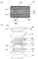
図1は、本発明の第1の実施形態に係る電子部品X1を表し、(a)はそのA−A’断面図であり、(b)はその分解斜視図である。電子部品X1は、複数(本実施形態では4つ)の誘電体層10と、コイル状導体20と、一対の接地導体層30とを備える。
1A and 1B show an electronic component X1 according to a first embodiment of the present invention, in which FIG. 1A is a cross-sectional view taken along line A-A ′, and FIG. 1B is an exploded perspective view thereof. The electronic component X1 includes a plurality (four in this embodiment) of
誘電体層10は、酸化アルミニウム質焼結体やガラスセラミック焼結体,窒化アルミニウム質焼結体,ムライト質焼結体等のセラミック焼結体、エポキシ樹脂,ポリイミド樹脂等の有機樹脂、または酸化アルミニウム等の無機粉末をエポキシ樹脂等の有機樹脂で結合してなる複合材料等の電気絶縁材料により形成されている。
The
ここで、誘電体層10を構成する材料として酸化アルミニウム質焼結体を採用した場合における積層体の作製方法の一例について説明する。まず、酸化アルミニウム(アルミナ)やガラスなどの原料粉末を有機溶剤やバインダなどと混合して泥漿状のセラミックスラリーを作製する。次に、作製されたセラミックススラリーを所定のシート成形技術(例えば、ドクターブレード法やカレンダーロール法)によりシート状に成形して、セラミックグリーンシート(セラミック生シート)を得る。次に、得られたセラミックグリーンシートを所定の順に上下に積層して生セラミックの積層体と成す。次に、この生セラミック成形体を還元雰囲気中で約1300〜1600℃の高温で焼成する。以上のようにして、積層体は作製される。なお、誘電体層10の作製方法としては、上述の作製方法に限られず、上記樹脂を用いて射出成形やトランスファー成形により作製するようにしてもよい。
Here, an example of a method for producing a laminated body in the case where an aluminum oxide sintered body is employed as a material constituting the
コイル状導体20は、周回パターン21、22およびビア導体23を有し、周回パターン21と周回パターン22とをビア導体23により電気的に接続することにより形成されている。また、コイル状導体20は、上記積層体の内部に埋設されている。
The coiled conductor 20 includes the
コイル状導体20に電流が流れると、各周回パターン21、22にいわゆる右ねじの進む向きに磁界が発生する。各周回パターン21、22で生じる磁束が同一方向になって磁界が強められ、このコイル内部に磁界の強さ(H)に応じたインダクタンスが発生する。磁界の強さは、コイルの巻数に比例するので、周回パターン21、22の積層数(本実施形態では2つ)を調整することにより、所定の強さの磁界を発生させることができる。そして、この磁界により生じるインダクタンスにより、電子部品X1は、例えばインダクタとして機能する。
When a current flows through the coiled conductor 20, a magnetic field is generated in each of the
周回パターン21のパターン幅W1は、周回パターン22のパターン幅W2よりも狭くなるように構成されている。また、周回パターン21は、その内周および外周が上記積層体を平面透視して、周回パターン22の幅方向における内側に位置する部位を有する。
The pattern width W1 of the
周回パターン21、22およびビア導体23構成する材料としては、タングステン、モリブデン、マンガン、銅、銀、金、パラジウム、白金等の金属材料が挙げられる。
Examples of the material constituting the
ここで、周回パターン21、22を構成する材料として銅を採用した場合における周回パターン21、22の形成方法の一例について説明する。まず、銅ペーストを用意する。次に、この銅ペーストを、誘電体層10となるセラミックグリーンシートの表面に対して所定の印刷手法(例えば、スクリーン印刷法)で印刷する。以上のようにして、周回パターン21、22が形成される。
Here, an example of a method of forming the
また、ビア導体23は、例えば、誘電体層10となるセラミックグリーンシートの所定部位(上下の周回パターン間を接続させる部位)に貫通孔(図示せず)を形成しておいて、その貫通孔に、周回パターン21、22を形成するのと同様の金属ペーストを充填することにより形成することができる。
In addition, the via
周回パターン21、22は、例えば、四角形状の誘電体層10の層間の外周に沿って形成された枠状や環状等のパターンであり、層間の全周にわたるものや一部に非形成部を有するものを含む。
The
接地導体層30は、周回パターン21、22に対して上記積層体の積層方向両側にコイル状導体20を間に挟んで対向するように設けられている。
The
本実施形態に係る電子部品X1では、合計3個の周回パターン21、22のうち1個の周回パターン21のパターン幅W1がその上下に位置する周回パターン22のパターン幅W2よりも狭くされている。そのため、電子部品X1では、上下の誘電体層10の間で位置ずれ(積層ずれ)が生じたとしても、周回パターン21が、平面視で、その上下に隣り合う周回パターン22と重なる領域から外れ難くなるので、周回パターン22の間で、周回パターン21間の位置ずれや、重なりの位置のずれ、重なりの幅のずれなどの発生が抑制される。したがって、電子部品X1では、上下の周回パターン22同士の対向する面積(や対向する位置)が所定値から大きくずれるようなことは抑制されるので、新たなキャパシタンスの発生を抑制することができる。
In the electronic component X1 according to this embodiment, the pattern width W1 of one of the three
電子部品X1は、コイル状導体20が隣接する誘電体層10間に介在されている3個の周回パターン21、22を、少なくとも一部が上記積層体の積層方向に隣接する他の周回パターン21、22と平面透視して重なるように配置させた上、ビア導体23を介して電気的に接続して成る。したがって、電子部品X1は、周回パターン21、22の数を充分に確保して、Q値の高いインダクタを小型に形成することができる。
The electronic component X1 includes three
電子部品X1は、上記積層体が4層の誘電体層10を積層して成り、コイル状導体20に対して上記積層体の積層方向両側にコイル状導体20を間に挟んで対向する一対の接地導体層30が配置されている。そのため、電子部品X1では、コイル状導体20に強い磁界が発生した場合においても、その磁界は、コイル状導体の中心部を、コイル状導体の一方の端から他方の端にかけて(積層方向に)貫通する磁束により形成されるので、これら一対の接地導体層30で遮断され、外部に漏れることが抑制される。したがって、電子部品X1では、他の電子部品などに磁界による影響を与えるのを抑制することができるので、より信頼性の高い電子機器(携帯電話や無線LAN等の通信装置、コンピュータ)等を構成することが可能な電子部品とすることができるのである。
The electronic component X1 is formed by stacking four
電子部品X1では、周回パターン21の内周及び外周が、上記積層体を平面透視して、上下に配置されている周回パターン22の内側に位置する部位を有する。そのため、電子部品X1は、周回パターン21が実質的に全域で平面視で上下の周回パターン22と重なる。したがって、電子部品X1は、磁界がより有効に発生するため、Q値を高めるうえで好適である。
In the electronic component X <b> 1, the inner periphery and the outer periphery of the
図2は、本発明の第2の実施形態に係る電子部品X2を表し、(a)はそのB−B’断面図であり、(b)はその分解斜視図である。電子部品X2は、誘電体層10において、接地導体層30と接地導体層30に対して積層方向で隣り合う周回パターン22との間の厚さを積層方向に隣り合う周回パターン21,22どうしの間の厚さよりも大きいものとした点において、電子部品X1と異なる。電子部品X2の他の構成については、電子部品X1に関して上述したのと同様である。
2A and 2B show an electronic component X2 according to the second embodiment of the present invention, in which FIG. 2A is a B-B ′ sectional view and FIG. 2B is an exploded perspective view thereof. In the electronic component X2, in the
なお、誘電体層10において、接地導体層30と接地導体層30に対して積層方向で隣り合う周回パターン22との間の厚さを積層方向に隣り合う周回パターン21、22どうしの間の厚さよりも大きいものとする方法としては、例えば、接地導体層30と接地導体層30に対して積層方向で隣り合う周回パターン22との間において、誘電体層10を構成するセラミックグリーンシート自体の厚さを厚くする方法や、積層する層数を多くする方法などが挙げられる。
In the
本実施形態に係る電子部品X2は、接地導体層30と接地導体層30に対して積層方向で隣り合う周回パターン22との間に介在する誘電体の厚さが大きい。そのため、電子部品X2では、互いに対向する接地導体層30および周回パターン22を容量電極として両者間に生じるキャパシタンスは効果的に低く抑えることができる。したがって、電子部品X2は、Q=1/ωcR(ω:角周波数(周回パターンを通る電気信号の周波数)、c:キャパシタンス(周回パターンと接地導体層との間に生じるキャパシタンス)、R:抵抗(周回パターンの電気抵抗))の関係式より、Q値を高めるうえで好適であることがわかる。
In the electronic component X2 according to this embodiment, the thickness of the dielectric interposed between the
本発明の第3の実施形態に係る電子部品X3は、誘電体層10において、接地導体層30と、接地導体層30に対して積層方向で隣り合う周回パターン22との間の比誘電率が積層方向に隣り合う周回パターン21、22間の比誘電率よりも小さいものとした点において、電子部品X1と異なる。電子部品X3の他の構成については、電子部品X1に関して上述したのと同様である。
In the electronic component X3 according to the third embodiment of the present invention, the
なお、誘電体層10において、接地導体層30と、接地導体層30に対して積層方向で隣り合う周回パターン22との間の比誘電率を、積層方向に隣り合う周回パターン21、22間の比誘電率に比し小さくする方法としては、例えば、誘電体層10に、銀(Ag)、アルミニウム(Al)、ケイ素(Si)などの金属複合酸化物(例えばAgO3、Al2O3、SiO2など)を添加する方法などが挙げられる。
In the
本実施形態に係る電子部品X3は、接地導体層30と、接地導体層30に対して積層方向で隣り合う周回パターン22との間に介在する誘電体の比誘電率が小さい。そのため、電子部品X3では、互いに対向する接地導体層30および周回パターン22を容量電極として両者間に生じるキャパシタンスを効果的に低く抑えることができる。したがって、本電子部品は、上記関係式より、Q値を高めるうえで好適であることがわかる。
In the electronic component X3 according to the present embodiment, the relative dielectric constant of a dielectric interposed between the
図3は、本発明の第4の実施形態に係る電子部品X4を表し、(a)はC−C’断面図であり、(b)はその分解斜視図である。電子部品X4は、一対の接地導体層30が、積層体を厚み方向に貫通する少なくとも1つの貫通導体40を介して互いに電気的に接続されている点において、電子部品X1と異なる。電子部品X4の他の構成については、電子部品X1に関して上述したのと同様である。図3において図1と同じ部位には同じ符号を付している。
3A and 3B show an electronic component X4 according to the fourth embodiment of the present invention, in which FIG. 3A is a C-C ′ cross-sectional view and FIG. 3B is an exploded perspective view thereof. The electronic component X4 differs from the electronic component X1 in that the pair of ground conductor layers 30 are electrically connected to each other via at least one through
本実施形態に係る電子部品X4は、一対の接地導体層30は、積層体を厚み方向に貫通する少なくとも1つの貫通導体40を介して互いに電気的に接続されていることから、一対の接地導体層30はより低いインダクタとなる。そのため、接地電位がより一層安定し、コイル状導体20と外部との電磁的な遮蔽がより有効に行なわれるため、コイル状導体20に強い磁界が発生した場合においても、これら一対の接地導体層30により磁力が外部に漏れるのをより効率よく抑制することができる。したがって、本電子部品X4では、外部に対する電磁的な影響(ノイズ漏れ等)を、より効果的に抑制することができる。
In the electronic component X4 according to this embodiment, the pair of ground conductor layers 30 are electrically connected to each other via at least one through
貫通導体40は、例えば、ビア導体23と同様の材料および方法により形成することができる。貫通導体40が銅で形成されている場合であれば、例えば、誘電体層10となる複数のセラミックグリーンシートに、積層した際に、上層から下層まで連通するように貫通孔(図示せず)を形成し、その貫通孔に銅ペーストを充填することにより、貫通導体40が形成される。
The through
本発明の電子部品X1〜X4において、3個以上の周回パターン21、22の、それぞれの周回パターンにおける、各幅方向の中央部を通る中心線の長さが、上下に位置する周回パターン22よりも幅の狭い周回パターン21が長いことが好ましい。
In the electronic components X1 to X4 of the present invention, the length of the center line passing through the central part in each width direction in each of the three or
この構成により、互いに対向する接地導体層30からのキャパシタンスの影響をほとんど受けない幅の狭い周回パターン21(上下の各接地導体層30との間に他の周回パターン22が介在するため)が、コイル状導体の周回パターン全長に対する割合が大きくなる。そのため、本電子部品では、誘電体層10間で位置ずれが生じ、その位置ずれに起因して上下の周回パターン21、22間で、位置ずれが起きても、キャパシタンスの変わらない、より電気特性が安定した電子部品とすることができる。
With this configuration, a narrow
また、3個以上の周回パターン21、22の、それぞれの周回パターン21、22における、各幅方向の中央部を通る中心線の長さを、上下に位置する周回パターン22よりも幅の狭い周回パターン21が長いようにする場合、幅の狭い周回パターン21の中心線の長さが、上に位置する周回パターン22と接続されるビア導体23を始点として、下に位置する周回パターン22と接続されるビア導体23までの長さであり、上下に位置する周回パターン22の長さが、幅の狭い周回パターン21と接続されるビア導体23を始点として、コイル状導体20の開始部または終端部までの長さであることがより一層好ましい。
Moreover, the length of the center line which passes through the center part of each width direction in each of the three or more
この構成により、互いに対向する接地導体層30からのキャパシタンスの影響をほとんど受けない幅の狭い周回パターン21の有効な長さが、有効なコイル状導体の周回パターン全長に対する割合が大きくなる。そのため、本電子部品では、誘電体層10間で位置ずれが生じ、その位置ずれに起因して上下の周回パターン21、22間で、位置ずれが起きても、キャパシタンスの変わらない、より安定した電子部品とすることができる。
With this configuration, the effective length of the narrow
また、本発明の電子部品X1〜X4において、3個以上の周回パターン21、22の内周および外周の角部が、円弧状に形成されていることが好ましい。
Moreover, in the electronic components X1 to X4 of the present invention, it is preferable that the inner and outer corners of the three or
この場合、上下に位置する周回パターン22と幅の狭い周回パターン21が、積層時にたとえ回転ずれ(θずれ)を起こしても、幅の狭い周回パターン21の角部が上下に位置する周回パターン22の角部より平面視で飛び出すことが抑制される。
In this case, even if the
したがって、本電子部品は、互いに対向する接地導体層30からのキャパシタンスの影響を受けることなく、よりQ値を高くすることができる。 Therefore, this electronic component can further increase the Q value without being affected by the capacitance from the ground conductor layers 30 facing each other.
あわせて、上下の周回パターン21、22同士の対向する面積(や対向する位置)が所定値から大きくずれるようなことはより確実に抑制される。
In addition, it is more reliably suppressed that the area (or the position at which they face each other) between the upper and lower
なお、周回パターン21、22の角部を円弧状にする場合、上下の周回パターン21、22の間で円弧の曲率半径を同じにしておくのが好ましく、さらに、外周側と内周側とで曲率半径がほぼ同心半径であることが、より好ましい。このような形状とすることにより、積層時にたとえ回転ずれ(θずれ)を起こしても、幅の狭い周回パターン21の角部が上下に位置する周回パターン22の角部より平面視で飛び出すことが、より抑制される。
In addition, when making the corner | angular part of the
以上、本発明の具体的な実施形態を示したが、本発明はこれに限定されるものではなく、発明の思想から逸脱しない範囲内で種々の変更が可能である。 Although specific embodiments of the present invention have been described above, the present invention is not limited to these embodiments, and various modifications can be made without departing from the spirit of the invention.
電子部品X1は、単独でインダクタとして用いられるものに限らず、インダクタンスの機能を内蔵するとともに他の機能(アンテナの機能や、半導体素子や圧電素子、センサ素子等の電子部品素子搭載の機能等)を備えたものでもよい。 The electronic component X1 is not limited to being used alone as an inductor, but has a built-in inductance function and other functions (an antenna function, a function of mounting an electronic component element such as a semiconductor element, a piezoelectric element, or a sensor element). May be provided.
X 電子部品
10 誘電体層
20 コイル状導体
21,22 周回パターン
23 ビア導体
30 接地導体層
40 貫通導体
Claims (9)
Priority Applications (1)
| Application Number | Priority Date | Filing Date | Title |
|---|---|---|---|
| JP2006082227A JP2007123802A (en) | 2005-07-28 | 2006-03-24 | Electronic component |
Applications Claiming Priority (3)
| Application Number | Priority Date | Filing Date | Title |
|---|---|---|---|
| JP2005218308 | 2005-07-28 | ||
| JP2005283012 | 2005-09-28 | ||
| JP2006082227A JP2007123802A (en) | 2005-07-28 | 2006-03-24 | Electronic component |
Publications (1)
| Publication Number | Publication Date |
|---|---|
| JP2007123802A true JP2007123802A (en) | 2007-05-17 |
Family
ID=38147266
Family Applications (1)
| Application Number | Title | Priority Date | Filing Date |
|---|---|---|---|
| JP2006082227A Pending JP2007123802A (en) | 2005-07-28 | 2006-03-24 | Electronic component |
Country Status (1)
| Country | Link |
|---|---|
| JP (1) | JP2007123802A (en) |
Cited By (2)
| Publication number | Priority date | Publication date | Assignee | Title |
|---|---|---|---|---|
| CN102087911A (en) * | 2009-12-08 | 2011-06-08 | 上海华虹Nec电子有限公司 | Unequal-width on-chip stacked inductor with metals of unequal thicknesses |
| JP2020202255A (en) * | 2019-06-07 | 2020-12-17 | 株式会社デンソー | Electronic apparatus |
-
2006
- 2006-03-24 JP JP2006082227A patent/JP2007123802A/en active Pending
Cited By (3)
| Publication number | Priority date | Publication date | Assignee | Title |
|---|---|---|---|---|
| CN102087911A (en) * | 2009-12-08 | 2011-06-08 | 上海华虹Nec电子有限公司 | Unequal-width on-chip stacked inductor with metals of unequal thicknesses |
| US8441333B2 (en) | 2009-12-08 | 2013-05-14 | Shanghai Hua Hong Nec Electronics Company, Limited | Stack inductor with different metal thickness and metal width |
| JP2020202255A (en) * | 2019-06-07 | 2020-12-17 | 株式会社デンソー | Electronic apparatus |
Similar Documents
| Publication | Publication Date | Title |
|---|---|---|
| KR100899561B1 (en) | Laminated coil component | |
| US6498555B1 (en) | Monolithic inductor | |
| JP2005167130A (en) | Laminated electronic component and method for manufacturing the same | |
| WO2017018134A1 (en) | Multilayer substrate and electronic device | |
| JP5078340B2 (en) | Coil built-in board | |
| US6992556B2 (en) | Inductor part, and method of producing the same | |
| CN212163292U (en) | Composite electronic component and electronic circuit | |
| KR20070032259A (en) | Ultra-thin flexible inductor | |
| JP2007123802A (en) | Electronic component | |
| JP2005167468A (en) | Electronic apparatus and semiconductor device | |
| JP5472717B2 (en) | Coupler | |
| JP3658350B2 (en) | Manufacturing method of multilayer chip balun element | |
| JP4295660B2 (en) | Balun transformer | |
| JP5294319B2 (en) | Multilayer chip balun element | |
| JP4298211B2 (en) | Multilayer inductor | |
| WO2019088252A1 (en) | Lc resonance antenna | |
| JP4788419B2 (en) | Common mode noise filter | |
| JP5884968B2 (en) | Multilayer resonator | |
| JP2003197427A (en) | Inductance element | |
| JP6473210B1 (en) | LC resonant antenna | |
| JP2019024186A (en) | Rfid tag and article including the same | |
| JP2012138534A (en) | Stacked electronic component | |
| JP2009055073A (en) | High-frequency circuit element | |
| JP2004071962A (en) | Laminated inductor | |
| JP2009239487A (en) | Planar antenna element and manufacturing method thereof |