JP2007123731A - Semiconductor light emitting element and semiconductor light emitting device - Google Patents
Semiconductor light emitting element and semiconductor light emitting device Download PDFInfo
- Publication number
- JP2007123731A JP2007123731A JP2005317038A JP2005317038A JP2007123731A JP 2007123731 A JP2007123731 A JP 2007123731A JP 2005317038 A JP2005317038 A JP 2005317038A JP 2005317038 A JP2005317038 A JP 2005317038A JP 2007123731 A JP2007123731 A JP 2007123731A
- Authority
- JP
- Japan
- Prior art keywords
- semiconductor
- layer
- light emitting
- emitting device
- light
- Prior art date
- Legal status (The legal status is an assumption and is not a legal conclusion. Google has not performed a legal analysis and makes no representation as to the accuracy of the status listed.)
- Pending
Links
Images


Landscapes
- Semiconductor Lasers (AREA)
- Led Devices (AREA)
Abstract
【課題】発光効率が高く、演色性が高い半導体発光素子および半導体発光装置を提供することを可能にする。
【解決手段】基板1上に設けられた第1導電型半導体からなる第1半導体層4と、第1半導体層上に設けられた第2導電型半導体からなる第2半導体層8と、第1半導体層と第2半導体層との間に設けられ、第1および第2半導体層の半導体の禁止帯幅より小さい禁止帯幅を有する半導体材料の複数の量子ドット6aを含み、駆動電流に応じて基底準位あるいは励起準位に対応した波長の光を発光する発光層6と、を備えている。
【選択図】図1It is possible to provide a semiconductor light emitting element and a semiconductor light emitting device with high luminous efficiency and high color rendering.
A first semiconductor layer made of a first conductivity type semiconductor provided on a substrate, a second semiconductor layer made of a second conductivity type semiconductor provided on the first semiconductor layer, and a first semiconductor layer. A plurality of quantum dots 6a made of a semiconductor material, which is provided between the semiconductor layer and the second semiconductor layer and has a forbidden band width smaller than the forbidden band widths of the semiconductors of the first and second semiconductor layers. And a light emitting layer 6 that emits light having a wavelength corresponding to the ground level or the excitation level.
[Selection] Figure 1
Description
本発明は、半導体発光素子および半導体発光装置に関する。 The present invention relates to a semiconductor light emitting element and a semiconductor light emitting device.
窒化ガリウム系半導体は、その光学遷移が直接遷移型であるため高効率の発光再結合が可能である。最も良く用いられる窒化ガリウム系半導体であるInxGal−xNからなる3元混晶は、Inの組成比xを調節することにより、禁止帯幅(バンドギャップエネルギー)をGaNの3.4eV(364nm)からInNの0.7eV(1770nm)まで変えることができる。このため、InGaNからなる混晶材料のみで近紫外域、可視光、近赤外域までの波長帯をカバーする発光素子の活性層として用いることができる。現在のところ、このInGaNからなる混晶材料を発光層として用いたLED(Light Emitting Diode)が実現され、また半導体レーザにおいても電流注入によるレーザ発振が実現されている。 Since the optical transition of the gallium nitride based semiconductor is a direct transition type, highly efficient light emission recombination is possible. A ternary mixed crystal composed of In x Ga l-x N, which is the most commonly used gallium nitride semiconductor, has a band gap energy of 3.4 eV of GaN by adjusting the In composition ratio x. (364 nm) to 0.7 eV (1770 nm) of InN. For this reason, it can use as an active layer of the light emitting element which covers the wavelength range to a near ultraviolet region, visible light, and a near infrared region only with the mixed crystal material which consists of InGaN. At present, LEDs (Light Emitting Diodes) using this InGaN mixed crystal material as a light emitting layer have been realized, and laser oscillation by current injection has also been realized in semiconductor lasers.
近年、窒化ガリウム(GaN)系材料による短波長半導体レーザあるいは可視発光ダイオード(LED)は、発光再結合の効率が飛躍的に向上し、実用化され、青色や白色の発光が可能となり、LEDの適用範囲が大きく広がっている。このなかで白色発光素子は、液晶表示装置のバックライトへの適用にとどまらず、白熱電灯や蛍光灯に取って代わる可能性を秘めており、これまでに多くの提案がなされている。しかし、InGaNからなる混晶材料の問題点として、結晶成長が困難とされるミスシビリティギャップの存在がある。このため、現在のところ実現されている可視光LEDは、InGaNの混晶材料からなる発光層を薄膜化して歪み格子系の接合を形成し、この格子歪エネルギーによって得られる準安定領域を用いてその結晶成長を可能にしている。しかしながら、このようにして成長した混晶は、もともと不安定であるために、電流注入により発生する熱やデバイスの使用環境条件などの影響を受けやすく、これらが原因で特性劣化を起こしてしまうという問題があった。また、特に緑色や黄色に対応する長波長の発光素子では、Inの組成比xが高い混晶が必要とされるが、結晶の安定性はInの組成比の増加と共に低下していく。従って、従来はこれらの混晶系を用いた半導体発光素子において、高出力と長寿命とを実現することが困難であった。 In recent years, short-wavelength semiconductor lasers or visible light-emitting diodes (LEDs) made of gallium nitride (GaN) -based materials have dramatically improved the efficiency of light-emitting recombination, have been put into practical use, and can emit blue and white light. The scope of application is greatly expanded. Among these, the white light emitting element is not limited to the application to the backlight of the liquid crystal display device, and has the potential to replace incandescent lamps and fluorescent lamps, and many proposals have been made so far. However, there is a miscibility gap that makes crystal growth difficult as a problem of mixed crystal materials made of InGaN. For this reason, the visible light LED currently being realized uses a metastable region obtained from this lattice strain energy by forming a light-emitting layer made of a mixed crystal material of InGaN into a thin film and forming a strained lattice system junction. The crystal growth is possible. However, the mixed crystal grown in this way is inherently unstable, so it is easily affected by the heat generated by current injection and the environmental conditions of the device, which causes characteristic deterioration. There was a problem. In particular, long-wavelength light emitting elements corresponding to green and yellow require a mixed crystal having a high In composition ratio x, but the stability of the crystal decreases as the In composition ratio increases. Therefore, conventionally, it has been difficult to achieve high output and long life in semiconductor light emitting devices using these mixed crystal systems.
これに対して、GaNの量子ドットを形成して、この量子ドットのサイズを変えることにより、青色から赤色の発光、さらにこれらを組み合わせ白色の発光を得た実験結果が示されている(例えば、非特許文献1参照)。この実験結果では、GaNの量子ドットから発光する光の波長がバルク材料のGaN(バンドギャップエネルギー(3.4eV))の発光波長よりも長くなるのは、AlNに挟まれたGaNが、格子不整合から生じる大きな歪みを受け、ピエゾ電界効果により、非常に強いビルトイン電界(例えば、約5.5MV/cm)を受け、量子閉じ込めシュタルク効果(QCSE(Quantum Confined Stark Effect))により、発光波長が長波長側にシフトしたためと説明されている。 On the other hand, by forming GaN quantum dots and changing the size of the quantum dots, experimental results are shown in which blue to red light emission and further white light emission are obtained by combining these (for example, Non-patent document 1). In this experimental result, the wavelength of light emitted from the GaN quantum dots is longer than the emission wavelength of the bulk material GaN (band gap energy (3.4 eV)). Due to the large distortion resulting from the matching, the piezo electric field effect causes a very strong built-in electric field (for example, about 5.5 MV / cm), and the quantum confined Stark effect (QCSE (Quantum Confined Stark Effect)) causes a long emission wavelength. It is explained that it has shifted to the wavelength side.
また、InGaNの量子井戸からなる活性層を用いた青色LEDと、黄色を中心に発光するYAG(Yttrium Aluminum Garnet)蛍光体とを組み合わせる白色発光素子が、提案されている(例えば特許文献1参照)。この白色発光素子では、YAG蛍光体を青色光で励起し、青色光と黄色光との混合によって白色光を得る。 Further, a white light emitting element is proposed that combines a blue LED using an active layer made of an InGaN quantum well and a YAG (Yttrium Aluminum Garnet) phosphor that emits light mainly in yellow (see, for example, Patent Document 1). . In this white light emitting device, the YAG phosphor is excited with blue light, and white light is obtained by mixing blue light and yellow light.
また、InとGaとを含む窒化物半導体内の単一層領域において2つ以上の発光スペクトルピークを発光する発光素子が提案されている(例えば、特許文献2参照)。この発光素子では、単一層内においてIn組成比が異なる2以上の混晶領域を形成し、各混晶領域でバンドギャップが相違すること、すなわち発光波長が変化することを利用する。 In addition, a light-emitting element that emits two or more emission spectrum peaks in a single layer region in a nitride semiconductor containing In and Ga has been proposed (see, for example, Patent Document 2). In this light-emitting element, two or more mixed crystal regions having different In composition ratios are formed in a single layer, and the fact that the band gap is different in each mixed crystal region, that is, the emission wavelength is changed.
また、窒化物半導体の発光層内に2以上のスペクトルピークを含む光を発光する多重構造を備えた発光素子が提案されている(例えば、特許文献3参照)。この多重構造を含む発光層は、複数の井戸層を有する多重量子井戸からなっている。この2つ以上のスペクトルピークを含む光は混合されて、白色光を提供する。 In addition, a light-emitting element having a multiple structure that emits light including two or more spectral peaks in a light-emitting layer of a nitride semiconductor has been proposed (see, for example, Patent Document 3). The light emitting layer including the multiple structure is composed of a multiple quantum well having a plurality of well layers. The light containing the two or more spectral peaks is mixed to provide white light.
現在、人間の身の回りにありふれている目に見える光、すなわち可視光を使って通信を行う光通信技術が検討、普及しようとしている。オフィスや家の中や道路上の照明や、交通信号機や広告用電光掲示、ディスプレイ、電子機器の表示などの可視光を発する装置に使用されるLEDを高速変調させることにより、データ送信する。したがって、赤色(R)、緑色(G)、青色(B)の3色のLED、または青色LEDと黄色LEDの2色(BY)のLEDを組み合わせた白色発光素子は、照明などの機能だけでなく、それぞれのLEDでデータ通信が行え、また色多重化による伝送容量の増大を図ることが期待できる。
しかしながら、上記の従来例では、以下のような問題がある。 However, the above conventional example has the following problems.
非特許文献1では、形成したGaNの量子ドットのサイズを変化させることにより青色から赤色の発光が得られているが、ここでピエゾ電界を発光層に印加することにより発光される発光波長をバルクのバンド端波長から大きく変化させている。Inの混晶比が低くても、長波長側に大きく発光波長をシフトさせることができるようになるという利点を持つ反面、量子ドット(井戸)層内に生じるピエゾ電界が大きくなると、電子と正孔が空間的に分離され、それに伴い、電子と正孔のそれぞれの波動関数の重なる領域の積分値が小さくなり、発光再結合が著しく低下するという問題がある。
In
また、特許文献1乃至特許文献3の蛍光体を用いた白色発光素子では次のような問題がある。(1)蛍光材料の寿命が1万時間程度と短い、(2)蛍光体の光変換効率が100%にならず(ストークスシフト(Stokes Shift))、発光効率に原理的制約がある、(3)青色光の強度の増加につれて蛍光材料の発光強度が飽和する、などの問題がある。
Moreover, the white light emitting element using the phosphors of
また、単一層内のInの組成比が異なる混晶材料を用いて2つ以上の発光ピークを得る発光素子では、Inの組成不安定領域が形成される成長条件を用いて発光層を形成する。このため、Inの組成比の異なる混晶領域を安定して再現することができない。また、多重量子井戸構造により2つ以上の発光ピークを含む光を出す発光素子では、複数の井戸に電流注入して発光させるため、縦方向の電気抵抗が高くなることが避けられない。 Further, in a light-emitting element that obtains two or more emission peaks using mixed crystal materials having different In composition ratios in a single layer, the light-emitting layer is formed using a growth condition in which an In composition unstable region is formed. . For this reason, mixed crystal regions having different In composition ratios cannot be stably reproduced. In addition, in a light-emitting element that emits light including two or more light emission peaks by a multiple quantum well structure, current is injected into a plurality of wells to emit light, and thus the electrical resistance in the vertical direction is unavoidably increased.
また、赤色、緑色、青色の3色(RGB)のLED、または青色LEDと黄色LEDの2色(BY)のLEDを組み合わせた白色発光素子では、それぞれのLEDでデータ通信を行い、色多重化による伝送容量の増大が図ることが期待できるが、各LEDから出射される光はスペクトル幅が広く、青−緑、緑−赤など近接する波長において発光スペクトルが重畳し、各種フィルタなどを用いても分離できないという問題があり、白色発光素子において色多重化による伝送容量の増大は難しかった。LEDの発光スペクトルの狭帯域化を行うために、共振器構造を組み込んだRC−LED(Resonant-Cavity Light Emitting Diode)を用いることが有効であり、しかもこのRC−LEDは高速変調も可能となることから通信には好適であるが、白色発光素子のように複数個のLEDをRC−LEDに置き換えることは、多くの機器においてコストの面から導入は難しいと考えられる。 In the case of a white light emitting device combining red, green and blue three-color (RGB) LEDs, or a combination of blue and yellow LEDs (BY), data communication is performed with each LED, and color multiplexing is performed. However, the light emitted from each LED has a wide spectral width, and the emission spectrum is superimposed at close wavelengths such as blue-green and green-red. However, it is difficult to increase the transmission capacity by color multiplexing in the white light emitting element. To perform narrowing of the emission spectrum of the LED, it is effective to use that incorporates a resonator structure RC-LED (R esonant- C avity L ight E mitting D iode), yet the RC-LED fast Although modulation is also possible, it is suitable for communication, but replacing a plurality of LEDs with RC-LEDs such as white light-emitting elements is considered difficult to introduce in terms of cost in many devices.
本発明は、上記の課題を鑑み、発光効率が高く、演色性が高い半導体発光素子および半導体発光装置を提供することを目的とする。 In view of the above-described problems, an object of the present invention is to provide a semiconductor light-emitting element and a semiconductor light-emitting device that have high luminous efficiency and high color rendering.
本発明の第1の態様による半導体発光素子は、基板上に設けられた第1導電型半導体からなる第1半導体層と、前記第1半導体層上に設けられた第2導電型半導体からなる第2半導体層と、前記第1半導体層と前記第2半導体層との間に設けられ、前記第1および第2半導体層の半導体の禁止帯幅より小さい禁止帯幅を有する半導体材料の複数の量子ドットを含み、駆動電流に応じて基底準位あるいは励起準位に対応した波長の光を発光する発光層と、を備えたことを特徴とする。 The semiconductor light emitting device according to the first aspect of the present invention includes a first semiconductor layer made of a first conductive type semiconductor provided on a substrate, and a second conductive type semiconductor made of a second conductive semiconductor provided on the first semiconductor layer. A plurality of quantum layers of a semiconductor material provided between two semiconductor layers and between the first semiconductor layer and the second semiconductor layer and having a forbidden bandwidth smaller than that of the semiconductor of the first and second semiconductor layers And a light emitting layer that emits light having a wavelength corresponding to a ground level or an excitation level according to a driving current.
なお、複数の量子ドットは実質的に均一なサイズであってもよい。 The plurality of quantum dots may have a substantially uniform size.
なお、前記量子ドットは、サイズが1nm〜100nmであることが好ましい。 The quantum dots are preferably 1 nm to 100 nm in size.
また、本発明の第2の態様による半導体発光素子は、基板上に設けられた第1導電型半導体からなる第1半導体層と、前記第1半導体層上に設けられた第2導電型半導体からなる第2半導体層と、前記第1半導体層と前記第2半導体層との間に設けられ、前記第1および第2半導体層の半導体の禁止帯幅より小さい禁止帯幅を有する半導体材料からなる実質的に均一な幅の複数の量子細線を含む発光層と、を備えたことを特徴とする。 The semiconductor light emitting device according to the second aspect of the present invention includes a first semiconductor layer made of a first conductive type semiconductor provided on a substrate and a second conductive type semiconductor provided on the first semiconductor layer. And a semiconductor material provided between the first semiconductor layer and the second semiconductor layer and having a forbidden band width smaller than that of the semiconductor of the first and second semiconductor layers. And a light emitting layer including a plurality of quantum wires having a substantially uniform width.
また、本発明の第3の態様による半導体発光素子は、基板上に設けられた第1導電型半導体からなる第1半導体層と、前記第1半導体層上に設けられた第2導電型半導体からなる第2半導体層と、前記第1半導体層と前記第2半導体層との間に設けられ、前記第1および第2半導体層の半導体の禁止帯幅より小さい禁止帯幅を有する半導体材料の複数の量子細線を含み、駆動電流に応じて基底準位あるいは励起準位に対応した波長の光を発光する発光層と、を備えたことを特徴とする。 The semiconductor light emitting device according to the third aspect of the present invention includes a first semiconductor layer made of a first conductivity type semiconductor provided on a substrate and a second conductivity type semiconductor provided on the first semiconductor layer. A plurality of semiconductor materials provided between the second semiconductor layer and the first semiconductor layer and the second semiconductor layer and having a forbidden band width smaller than that of the semiconductor of the first and second semiconductor layers And a light emitting layer that emits light having a wavelength corresponding to a ground level or an excitation level according to a driving current.
なお、前記量子細線は、厚みおよび幅が1nm〜100nmであることが好ましい。 The quantum wire preferably has a thickness and a width of 1 nm to 100 nm.
なお、前記発光層は複数の波長で発光強度のピークを有し、
前記第1および第2半導体層の少なくとも一方の半導体層の前記発光層
とは反対側に設けられ、前記複数の波長の少なくとも一つの波長での発光波長の幅を狭くして各波長の分離が可能な多層膜反射鏡を更に備えていてもよい。
The light emitting layer has emission intensity peaks at a plurality of wavelengths,
The at least one semiconductor layer of the first and second semiconductor layers is provided on the opposite side of the light emitting layer, and the width of the light emission wavelength at at least one of the plurality of wavelengths is narrowed to separate each wavelength. A possible multilayer film reflecting mirror may be further provided.
なお、前記基板は、GaN、AlN、GaAs、Si、サファイア、SiC、ZnO、LiGaO2、ZrB2のうちのいずれかの材料からなっていてもよい。 The substrate may be made of any material selected from GaN, AlN, GaAs, Si, sapphire, SiC, ZnO, LiGaO 2 and ZrB 2 .
また、本発明の第4の態様による半導体発光装置は、同一基板上に設けられた請上記の半導体発光素子を複数個備え、前記半導体発光素子の駆動電流を変化させることにより、基底準位あるいは励起準位からの発光輝度を制御することを特徴とする。 According to a fourth aspect of the present invention, there is provided a semiconductor light-emitting device comprising a plurality of the above-described semiconductor light-emitting elements provided on the same substrate, and changing a driving current of the semiconductor light-emitting element to change a ground level or It is characterized by controlling emission luminance from an excitation level.
本発明によれば、発光効率が高く、演色性が高い半導体発光素子および半導体発光装置を提供することができる。 According to the present invention, it is possible to provide a semiconductor light-emitting element and a semiconductor light-emitting device that have high luminous efficiency and high color rendering.
以下、図面を参照して本発明の実施形態を説明する。 Hereinafter, embodiments of the present invention will be described with reference to the drawings.
(第1実施形態)
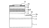
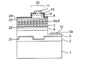
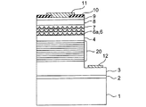
本発明の第1実施形態による半導体発光素子の断面を図1に示す。本実施形態の半導体発光素子はLED(発光ダイオード)であって、発光層6は、周りの半導体の禁止帯幅(バンドギャップエネルギー)より小さい禁止帯幅を有する半導体材料の3次元量子構造である量子ドット構造を有している。
(First embodiment)
FIG. 1 shows a cross section of the semiconductor light emitting device according to the first embodiment of the present invention. The semiconductor light emitting device of this embodiment is an LED (light emitting diode), and the
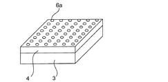
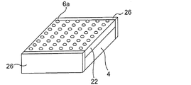
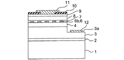
本実施形態のLEDは、厚さ300μmの(0001)面のサファイア(Al2O3の結晶)からなり表面及び裏面の両面が鏡面に研磨された単結晶基板1上に形成される。この単結晶基板1の表面に、GaNからなる膜厚20nmのバッファ層2と、Siが添加されたn形のGaNからなる膜厚4μmの電極層3と、Siが添加されたn形のAl0。1Ga0.9Nからなる膜厚0.5μmのクラッド層4と、が順次設けられている。なお、単結晶基板1は、サファイアに限るものではなく、例えば、窒化ガリウム(GaN)、シリコン(Si)、ガリウム砒素(GaAs)、炭化シリコン(SiC)や、酸化亜鉛(ZnO)や、リチウムガレート(LiGaO2)、ZrB2などの結晶から構成するようにしてもよい。また、n型クラッド層4上には、活性層6が設けられている。この活性層6は、図2に示すように、In0.65Ga0.35Nの組成からなる複数の実質的に均一なサイズに制御された量子ドット6aが同一平面に配列された構造の層であり、ここでは、量子ドット6aは直径20nm、高さ4nmの大きさに形成されている。量子ドット6aは、下地テンプレートを用いた選択成長の手法により形成され、その直径および高さは、同一面内での原子間力顕微鏡による測定から、平均直径20nm、平均高さ4nmに対して、それぞれの値の±5%の範囲内に半値幅が存在する分布となるように寸法制御されている。図2では、量子ドット6aを半球形状としているが、これに限るものではない。箱、円柱や角柱などの形状であってもよい。また図2では、量子ドット6aが下地テンプレートを用いて等間隔で、均一な密度に配列されているが、これに限るものではなく、各量子ドット6aの間隔が、不均一な状態で配置されていてもよい。また、量子ドット6aは、量子ドット6aを構成するInGaNの薄い膜でつながった状態に形成されていても良い。なお、量子ドット6aは、ほぼ同寸法に形成されているものである。以上のように複数の量子ドット6aから構成された活性層6は、ノンドープのGaNからなる膜厚10nmの成長カバー層(バリア層)7により覆われている。なお、本実施形態においては、活性層6と成長カバー層7との積層膜が3層に積層された構造となっており、第1の活性層は、クラッド層4上に形成され、第2および第3の活性層は成長カバー層7上に形成されている。成長カバー層7は量子ドット6aよりもバンドギャップエネルギーが大きい材料からなっている。
The LED of this embodiment is formed on a
また、最上層の成長カバー層7上には、Mgが添加されたp型のAl0.1Ga0.9Nからなる膜厚0.5μmのp型クラッド層8と、Mgが添加されたp形のGaNからなる膜厚0.1μmのコンタクト層9とが順次設けられている。また、コンタクト層9上には、電流注入領域を制限するための直径20μm程度の略円形の開口を備えたSiO2からなる電流制限絶縁層10が設けられている。この電流制限絶縁層10上には、上記開口を介してコンタクト層9に接触するp形金属電極11が設けられている。このp形金属電極11は、コンタクト層9に直接接触する膜厚50nmのニッケル層と、この上に形成された膜厚200nmの金層との積層構造となっている。なお、電極層3は、この電極層3上の各層を一部エッチングすることによって設けられた露出領域3aを有し、この露出領域3aにn形金属電極12が設けられている。このn形の金属電極12は、露出領域3aに直接接触する膜厚50nmのアルミニウム層と膜厚200nmの金層との積層構造となっている。
Further, on the uppermost
このように構成された本実施形態による半導体発光素子においては、発光層6は、InGaNからなる複数の量子ドット6aを有している。これらの量子ドット6aのサイズ、すなわち外径および高さが実質的に均一な構造となっている。なお、本明細書では、量子ドット6aの外径および高さが実質的に均一であるとは、外径および高さのそれぞれが、それぞれの平均値の±5%の範囲内に半値幅が存在する分布となっていることを意味する。
In the semiconductor light emitting device according to the present embodiment configured as described above, the
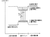
このような量子ドットの発光原理を、図3を参照して説明する。発光層6は、p型半導体層(本実施形態ではp型クラッド層8)とn型半導体層(本実施形態ではn型クラッド層4)とに挟まれており、外側から順方向電圧が印加され電流が注入されると、発光層6内にそれぞれの半導体層における多数キャリアが注入される。これらキャリアは、バンドギャップが小さい量子ドット中に流れ込み、量子ドット中に閉じ込められる。量子ドット内では、伝導帯に位置する電子と価電子帯に位置する正孔とが再結合して光を放出する。量子ドットのバンドギャップエネルギーは周囲の半導体層のバンドギャップエネルギーより小さいので、キャリアの閉じ込めが生じる。
The light emission principle of such quantum dots will be described with reference to FIG. The
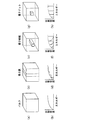
他方、発光層の形態を変えた場合の、エネルギーと状態密度との関係を図4(a)乃至図4(h)を参照して説明する。図4(a)に示すように発光層がバルクのときのエネルギーと状態密度との関係を図4(b)に、図4(c)に示すように発光層が量子膜のときのエネルギーと状態密度との関係を図4(d)に、図4(e)に示すように発光層が量子細線のときのエネルギーと状態密度との関係を図4(f)に、図4(g)に示すように発光層6が量子ドットのときのエネルギーと状態密度との関係を図4(h)に示す。図4(a)乃至図4(h)からわかるように、発光層がバルク、量子膜、量子細線、量子ドットと微少化されるにつれて、取り得るエネルギーも連続状態から離散状態に変化していく。
On the other hand, the relationship between energy and density of states when the form of the light emitting layer is changed will be described with reference to FIGS. 4 (a) to 4 (h). As shown in FIG. 4A, the relationship between energy and density of states when the light emitting layer is bulk is shown in FIG. 4B, and when the light emitting layer is a quantum film as shown in FIG. FIG. 4 (d) shows the relationship with the state density, FIG. 4 (f) shows the relationship between the energy and the state density when the light emitting layer is a quantum wire as shown in FIG. 4 (e), and FIG. As shown in FIG. 4, the relationship between the energy and the state density when the
図4(g)、(h)に示すように、量子ドットの場合は、微小領域へ電子、正孔が三次元的に閉じ込められ、伝導帯、価電子帯に量子サイズ効果により離散的なエネルギー準位が形成される。これにより、伝導帯、価電子帯の電子、正孔は、基底準位、第2準位などの完全に離散化された量子準位のみに局在し、量子ドットに電流を注入にして発光させる際に、駆動電流値を変化させると基底準位、第2準位などからの異なる遷移エネルギーからの電子・正孔再結合による発光が得られ、複数の波長が得られることになる(図3参照)。 As shown in FIGS. 4G and 4H, in the case of quantum dots, electrons and holes are three-dimensionally confined in a minute region, and discrete energy is generated in the conduction band and valence band due to the quantum size effect. A level is formed. As a result, electrons and holes in the conduction band and valence band are localized only in completely discrete quantum levels such as the ground level and the second level, and light is emitted by injecting current into the quantum dots. In this case, if the driving current value is changed, light emission by electron-hole recombination from different transition energies from the ground level, the second level, etc. is obtained, and a plurality of wavelengths are obtained (see FIG. 3).
したがって、本実施形態においては、量子ドット6aはその禁止帯幅および量子準位(励起準位)に対応した波長の光を発する。そして、量子ドット6aは、形状、外径、高さが実質的に均一な構造となっており、その寸法に対応した波長の光を発する。また、量子ドット6aは、そのバンドギャップエネルギーが周囲の半導体のバンドギャップエネルギーより小さく、そのキャリアが閉じ込められるので、高い発光効率で発光させることができる。このときの発光波長は量子ドット6aの外径に対応する。すなわち、量子ドット6aにおいては、微小領域への閉じ込めにより、伝導帯や価電子帯におけるエネルギー準位は離散化する。伝導帯、価電子帯の電子、正孔は、基底準位、第2準位などの完全に離散化された量子準位のみに局在することになる。量子ドット6aに電流を注入して発光させる際に、駆動電流値を変化させると基底準位、第二準位などからの発光が得られ、複数の波長での発光が得られる。
Therefore, in this embodiment, the
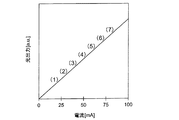
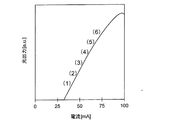
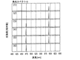
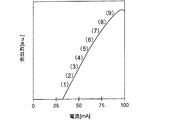
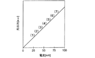
本実施形態によるLEDの駆動電流を変えた場合の、このLEDの出力特性を図5に示す。図5に示すように電流を増大した場合光出力は増大し、電流を(1)〜(7)と増大したときの本実施形態によるLEDの発光スペクトルを図6に示す。図6からわかるように、基底準位からの発光で中心波長が677nmの赤色光、励起準位の(量子ドット6aの高さ方向に直交する面内方向の閉じ込めにより形成された)第2準位からの発光で中心波長が562nmの緑色光、さらに励起準位の(量子ドット6aの高さ方向の閉じ込めにより形成された)第2準位からの発光で中心波長が462nmの青色光が得られる。
FIG. 5 shows the output characteristics of the LED when the drive current of the LED according to the present embodiment is changed. As shown in FIG. 5, when the current is increased, the light output increases, and the emission spectrum of the LED according to the present embodiment when the current is increased from (1) to (7) is shown in FIG. As can be seen from FIG. 6, red light having a central wavelength of 677 nm emitted from the ground level, the second level of the excitation level (formed by confinement in the in-plane direction perpendicular to the height direction of the
また、量子ドット6aのサイズが、その平均値の±5%の範囲内に半値幅が分布するように寸法制御されていることにより、発光波長は、基底準位からの発光では670nm〜684nmの波長、面内方向の閉じ込めにより形成された第2準位からの発光では547nm〜575nmの波長、高さ方向の閉じ込めにより形成された第2準位からの発光は443nm〜479nmの波長が得られ、何れの準位でも所望の波長域R、G、Bの3色が実現できることがわかった。
In addition, since the size of the
また、図5および図6からわかるように、本実施形態のLEDに流す電流が少ないと赤色の光が出力され、その後、電流を増大するにつれて赤色の光と、緑色の光が発生し、さらに電流を増大し(7)に対応する状態では赤色、緑色、青色の光が発生し、高輝度の白色の発光が得られる。 Further, as can be seen from FIGS. 5 and 6, when the current flowing through the LED of the present embodiment is small, red light is output, and thereafter, as the current is increased, red light and green light are generated. In a state corresponding to (7) when the current is increased, red, green, and blue light are generated, and high-luminance white light emission is obtained.
なお、本実施形態においては、量子ドット6aの寸法を電子のドブロイ波長以下とすることで、量子サイズ効果、高効率な発光が得られる。また、この量子ドット6aの寸法により、半導体発光素子から出射される複数の光の発光波長が決定される。
In the present embodiment, the quantum size effect and highly efficient light emission can be obtained by setting the size of the
(変形例)
本実施形態の変形例として、本実施形態において、活性層6を、In0.55Ga0.45Nの組成からなる複数の量子ドット6aを、直径10nm、高さ4nmの大きさに同一平面に形成したLEDを作成した。なお、本変形例においても、第1実施形態と同様に、量子ドット6aのサイズが、その平均値の±5%の範囲内に半値幅が分布するように寸法制御されている。
(Modification)
As a modification of the present embodiment, in the present embodiment, the
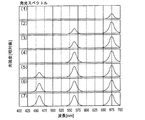
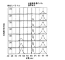
本変形例によるLEDの駆動電流を変えた場合の、本変形例の出力特性を図7に示す。図7に示すように電流を増大した場合光出力は増大し、電流を(1)〜(7)と増大したときの本変形例によるLEDの発光スペクトルを図8に示す。図8からわかるように、基底準位からの発光で中心波長が585nmの黄色光、励起準位の(量子ドットの面内方向の閉じ込めにより形成された)第2準位からの発光で中心波長が480nmの青色光、さらに励起準位の(量子ドットの高さ方向の閉じ込めにより形成された)第2準位からの発光で中心波長が415nmの青紫色光が得られた。 FIG. 7 shows output characteristics of this modification when the drive current of the LED according to this modification is changed. When the current is increased as shown in FIG. 7, the light output increases, and the emission spectrum of the LED according to this modification when the current is increased from (1) to (7) is shown in FIG. As can be seen from FIG. 8, yellow light having a central wavelength of 585 nm by light emission from the ground level, and central wavelength by light emission from the second level of the excitation level (formed by confinement in the in-plane direction of the quantum dots). Of blue light having a central wavelength of 415 nm by emission from the second level of the excited level (formed by confinement in the height direction of the quantum dots).
また、第1実施形態と同様に、量子ドット構造が±5%以下に寸法制御されていることにより、発光波長は、基底準位からの発光では波長580nm〜590nm、量子ドット6aの高さ方向に直交する面の面内方向の閉じ込めにより形成された第2準位からの発光では波長465nm〜490nm、量子ドットの高さ方向の閉じ込めにより形成された第2準位からの発光では波長400nm〜430nmが得られ、何れの準位でも所望の波長域の黄色、青色、青紫色の発光が実現できることがわかった。
Similarly to the first embodiment, since the quantum dot structure is dimensionally controlled to be ± 5% or less, the emission wavelength is 580 nm to 590 nm for emission from the ground level, and the height direction of the
そして、図7および図8からわかるように、第1実施形態と同様に、本変形例のLEDを適切な電流で駆動することにより、青色、青紫色、黄色の光が組み合わされ所望の高輝度の白色発光を得ることができる。 As can be seen from FIGS. 7 and 8, as in the first embodiment, by driving the LED of this modification with an appropriate current, blue, blue-violet, and yellow light are combined to obtain a desired high luminance. White light emission can be obtained.
(製造方法)
次に、図1に示した第1実施形態による半導体発光素子の製造方法について説明する。本実施形態においては、各結晶層を形成するための結晶成長には、縦型成長炉を有する有機金属気相成長装置を用いる。窒素原料は、アンモニアを用い、キャリアガスには水素ガスを用いる。また、成長圧力は常圧とする。
(Production method)
Next, a method for manufacturing the semiconductor light emitting device according to the first embodiment shown in FIG. 1 will be described. In the present embodiment, a metal organic vapor phase growth apparatus having a vertical growth furnace is used for crystal growth for forming each crystal layer. The nitrogen raw material uses ammonia and the carrier gas uses hydrogen gas. The growth pressure is normal pressure.
まず、基板温度を1050°とし、サファイアからなる結晶基板1の表面をアンモニア雰囲気で窒化した後、基板温度を550℃とし、GaNを成長させたバッファ層2を形成する。このGaNの成長において、ガリウム原料には比較的ガリウム蒸気圧の低いトリエチルガリウム(TEG)を用いる。引き続き、単結晶基板1を1050℃で9分間アニールし、バッファ層2の単結晶化を行う。
First, after the substrate temperature is set to 1050 ° and the surface of the
次に、単結晶基板1の温度を1020℃とし、Siが添加されたn形のGaNおよびSiが添加されたn形のAl0.1Ga0.9Nを順次成長させ、電極層3、クラッド層4を形成する。これら気相成長におけるアルミニウム原料は、トリメチルアルミニウム(TMA)を用い、ガリウム原料は比較的蒸気圧の高いトリメチルガリウム(TMG)を用いる。また、Siを各層に添加させるためには、水素で希釈した濃度1ppmのシラン(SiH4)ガスを用いる。
Next, the temperature of the
次いで、クラッド層4の上にInGaNをドット状に成長させて複数の量子ドット6aからなる活性層6を形成する。この量子ドット6aの形成においては、まず、下地となるクラッド層4に、幅70nmの正方形ナノホールがピッチ周期150nmで面方位に沿ってアレイ状に配置されたテンプレート構造を形成する。このテンプレート構造の形成は、電子線リソグラフィを用いて周期パターンを有するレジストパターンの作製およびこのレジストパターンをマスクとして塩素系ガスを用いたクラッド層4のドライエッチングにより行った。このときホールの深さは、所望の量子ドット6aの高さに合わせ、ドライエッチングの処理時間により調整した。エッチング処理後、レジストパターンを除去し、ウエハの化学薬品による洗浄を行う。その後、ウエハは再度、有機金属気相成長装置に戻され、水素雰囲気中の高温処理により自然酸化膜の除去処理を行った。ナノホールが形成されているクラッド層4上に再度。クラッド層と同じ材料を数モノレイア(ML)形成後、量子ドットとなるInGaNを成長させる。このとき、自己組織化した量子ドットが、ナノホールに選択的に配置、形成される。なお、公知の下地テンプレートを用いた選択成長法により、ドットは直径、高さは、それぞれ±4.8%、±5.0%以内に寸法制御されることが知られている(例えば、S. Kiravittaya et al., Applied Physics Letters 86, 206101 (2005) 参照)。
Next, InGaN is grown in the form of dots on the
本実施形態の製造方法によるInGaNの成長においては、金属インジウムの析出を防止して高品質InGaNを成長させ、かつ、下地上に吸着したインジウム原子のマイグレーションを促進させることを観点としてV族/III族との比と成長速度を設計し、量子ドット形状にInGaNを成長させる。 In the growth of InGaN by the manufacturing method of the present embodiment, from the viewpoints of preventing the deposition of metal indium to grow high quality InGaN and promoting the migration of indium atoms adsorbed on the substrate, the group V / III Design the ratio and growth rate with the family, and grow InGaN in the shape of quantum dots.
次いで、活性層6に対するエッチングやこの活性層6の結晶性の劣化を抑制するために、窒素キャリアガスを用いてInGaNと同じ成長温度である500℃でGaNを成長し、量子ドット6aを覆うように成長カバー層7を形成する。成長カバー層7は、InGaNからなる複数の量子ドット6aに対するバリア層となる。成長カバー層7を形成した後、基板1の温度を1020℃に上昇させて成長カバー層7の高品質化を図る。
Next, in order to suppress etching of the
引き続いて、Mgが添加されたp形Al0.1Ga0.9Nからなるクラッド層8およびマグネシウムが添加されたp形GaNからなるコンタクト層9を順次形成する。Mgを添加するための原料としては、メチルカプタン・ビスシクロペンタ・ジエニルマグネシウム(MeCP2Mg)を用いる。この原料は液体であり、一般に用いられている固体原料であるビスシクロペンタ・ジエニルマグネシウム(Cp2Mg)より、Mgの添加濃度の再現性が良い。クラッド層8、コンタクト層9を形成した後、これらの層の添加したMgの活性化を図るために、700℃の窒素雰囲気中で30分間アニールする。
Subsequently, a
次に、RFマグネトロン・スパッタ装置を用い、コンタクト層9上にSiO2からなる電流制限絶縁層10を形成し、これを公知のフォトリソグラフィ技術とエッチング技術とにより加工し、底面がコンタクト9の表面となる開口を電流制限絶縁層10に形成する。電流制限絶縁層10に開口を形成した後、電子ビーム蒸着装置を用い、開口内を含む電流制限絶縁層10上に、膜厚50nmのニッケル,膜厚100nmの金を順に蒸着して積層し、p型金属電極11となる金属層を形成する。この後、公知のフォトリソグラフィ技術により、金属層の上にポジ型フォトレジストのパターンを形成し、このパターンをマスクとして金属層11をエッチングしてp型金属電極11を形成するとともに、一部の領域の、金属層11、電流制限絶縁層10、コンタクト層9、クラッド層8、成長カバー層7、活性層6、およびクラッド層4を除去し、電極層3に露出領域3aを形成する。このエッチングにおいて、例えば、結晶層のエッチングでは、塩素ガスを用いた反応性イオンエッチングにより行えばよい。露出領域3aを形成するエッチングを行った後、フォトレジストのパターンを除去し、結晶基板1およびこの上に形成した構造体をクリーニングした後、電極層3の露出領域3aに膜厚50nmのアルミニウム、膜厚200nmの金を順に蒸着してこれらをパターニングすることにより、n型金属電極12を形成する。
Next, an RF magnetron sputtering apparatus is used to form a current limiting insulating
以上説明したことにより、n形金属電極12までを形成した後、これらを洗浄し、ダイヤモンド・スクライバを用いて単結晶基板1を所定の寸法に切断し、素子に切り出す。切り出した素子に所定の電流を印加して動作させれば、単結晶基板1の裏面側より光が発光される。
As described above, after forming up to the n-
上述したように、本実施形態においては、活性層を、島状に離散した複数の量子ドット6aから構成するようにした。言い換えると、活性層は、離散した量子井戸層の集合体あるいは、複数の量子ドットから構成されたものである。このように構成した半導体発光素子では、量子ドット6aの形状と、量子ドット6aを覆うように形成されている成長カバー層7の組成および厚さとに依存して発光波長が変化する。これは、InGaNからなる量子ドット6aに対する三次元的に加わる圧力(静水圧)によって、量子ドット6aを構成するInGaNのバンドギャップエネルギーが変化することによっている。InGaAlN系の材料では、従来の赤色用材料であるInGaAsP系の材料以上に広い範囲に渡って格子定数が異なっており、組成を変化させた層で覆うことで大きな静水圧を容易に加えることが可能である。従って、量子ドット6aのバンドギャップエネルギーを、InGaAsP系の材料に比較してより大きく変化させることが可能となる。このように大きくバンドギャップエネルギーを変化させることができるので、図1に示した本実施形態の半導体発光素子によれば、InNのバンドギャップ波長である1.6μm近傍からAlNのバンドギャップである紫外域に至る広い波長範囲の発光を得ることが可能となる。
As described above, in the present embodiment, the active layer is composed of a plurality of
以上述べたように、本実施形態によれば、発光効率が高く、演色性が高い半導体発光素子を提供することができる。 As described above, according to this embodiment, it is possible to provide a semiconductor light emitting device with high luminous efficiency and high color rendering.
(第2実施形態)
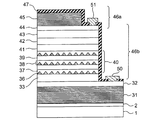
次に、本発明の第2実施形態による半導体発光素子の断面を図9に示す。この実施形態の半導体発光素子はレーザであって、次のように形成される。まず、サファイア基板1上に成長させた膜厚20nmの高品質GaNからなるバッファ層2に、フォトリソグラフィ技術と塩素系ガスを用いた反応性イオンエッチングとにより、幅10μm、深さ1.5μm、周期20μmの周期溝構造を<1−100>方向に沿って形成した。
(Second Embodiment)
Next, FIG. 9 shows a cross section of the semiconductor light emitting device according to the second embodiment of the present invention. The semiconductor light emitting device of this embodiment is a laser and is formed as follows. First, a
続いて、AlNからなる中間層21、電極層3、n型クラッド層4、膜厚120nmのアンドープAlGaNからなるガイド層22、活性層6、膜厚120nmのアンドープAlGaNからなるガイド層23、膜厚20nmのp型AlGaNからなるエッチングブロック層24、p型クラッド層8、コンタクト層9を順次積層し形成した。活性層6は第1実施形態の場合と同様に、均一なサイズの複数の量子ドット6aを有している。そして、同一面上に形成された複数の量子ドット6aは成長カバー層7によって覆われており、同一面上に形成された複数の量子ドット6aの層と、成長カバー層7とが交互に積層された三層積層構造となっている。
Subsequently, the
その後、コンタクト層9およびp型クラッド層8を、フォトリソグラフィ技術と塩素系ガスを用いた反応性イオンエッチングを用いてパターニングすることにより、リッジ幅5μm、共振器長900μmのリッジ導波路型構造25を形成する。
Thereafter, the
次に、リッジ導波路型構造25および露出したエッチングブロック層24を絶縁膜13で覆った後、リッジ導波路型構造25上の絶縁膜13に、底面がコンタクト層9に到達する開口を設ける。そして、この開口に金属を埋め込みパターニングすることにより、p型金属電極11を形成する。また、絶縁膜13、エッチングブロック層24、ガイド層23、活性層6、ガイド層22、クラッド層4、および電極層3をパターニングすることにより、電極層3に露出領域3aを形成し、この露出領域3a上にn型金属電極12を形成する。そして、図10に示すように端面の全面に反射層26を形成し、端面出射型のレーザ素子を作製した。
Next, after covering the
本実施形態のレーザ素子においては、図10に示すように、活性層6を、In0.55Ga0.45Nの組成からなる複数の量子ドット6aを平均直径10nm、平均高さ4nmの実質的に均一な大きさで同一平面に形成している。本実施形態においては、活性層6は3層構造となっているが、第1の活性層は、ガイド層22上に形成され、第2および第3の活性層は成長カバー層7上に形成されている。なお、本実施形態においても、第1実施形態と同様に、量子ドット6aのサイズが、その平均値の±5%の範囲内に半値幅が分布するように寸法制御されている。
In the laser device of the present embodiment, as shown in FIG. 10, the
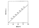
本実施形態によるレーザ素子の駆動電流を変えた場合の、本実施形態の出力特性を図11に示す。図11に示すように電流を増大した場合光出力は増大し、電流を(1)〜(6)と増大したときの本実施形態によるレーザ素子の発光スペクトルを図12に示す。図12からわかるように、基底準位からの黄色域のレーザ発振で中心波長が585nm、励起準位の(量子ドットの面内方向の閉じ込めにより形成された)第2準位からの青色のレーザ発振で中心波長が470nmのレーザ光が得られた。これにより、駆動電流を変化させることにより、黄色および青色の単色でのレーザ発振、青色と黄色が組み合わされた白色のレーザ発振が得られた。 FIG. 11 shows output characteristics of the present embodiment when the drive current of the laser device according to the present embodiment is changed. When the current is increased as shown in FIG. 11, the light output increases, and the emission spectrum of the laser device according to the present embodiment when the current is increased from (1) to (6) is shown in FIG. As can be seen from FIG. 12, the blue laser from the second level (formed by confinement in the in-plane direction of the quantum dots) at the central wavelength of 585 nm with laser oscillation in the yellow region from the ground level. A laser beam having a center wavelength of 470 nm was obtained by oscillation. As a result, by changing the drive current, laser oscillation in single colors of yellow and blue and white laser oscillation in which blue and yellow were combined were obtained.
(変形例)
また、変形例として、第2実施形態の活性層6を、In0.65Ga0.35Nの組成からなり直径10nm、高さ4nmの実質的に均一な大きさの複数の量子ドット6aからなる活性層に置き換えたレーザ素子を作成した。
(Modification)
As a modification, the
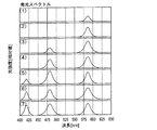
本変形例のレーザ素子に駆動電流を変えた場合の、本変形例の出力特性を図13に示す。図13に示すように電流を増大した場合光出力は増大し、電流を(1)〜(9)と増大したときの本変形例によるレーザ素子の発光スペクトルを図14に示す。図14からわかるように、基底準位からの赤色のレーザ発振で中心波長が630nm、励起準位の(量子ドットの面内方向の閉じ込めにより形成された)第2準位からの緑色のレーザ発振で中心波長が560nm、さらに励起準位の(量子ドットの高さ方向の閉じ込めにより形成された)第2準位からの青色のレーザ発振で中心波長が470nmのレーザ光が得られた。 FIG. 13 shows the output characteristics of this modification when the drive current is changed in the laser element of this modification. As shown in FIG. 13, the light output increases when the current is increased, and the emission spectrum of the laser device according to this modification when the current is increased from (1) to (9) is shown in FIG. As can be seen from FIG. 14, green laser oscillation from the second level of the excitation level (formed by confinement in the in-plane direction of the quantum dots) with a red laser oscillation from the ground level and a center wavelength of 630 nm. Thus, a laser beam having a center wavelength of 470 nm and a center wavelength of 470 nm was obtained by blue laser oscillation from the second level (formed by confinement in the height direction of the quantum dots) of the excitation level.
これにより、駆動電流を変化させることにより、赤色、緑色および青色の単色でのレーザ発振に加え、各色を組み合わした多彩な色でのレーザ発振を得ることができる。 Thus, by changing the drive current, in addition to laser oscillation in single colors of red, green, and blue, laser oscillation in various colors combining each color can be obtained.
また、本変形例のレーザ素子を用いて、駆動電流値の直接変調方式により、赤、緑、青のそれぞれの波長においてデータ通信が行えることを確認した。 In addition, it was confirmed that data communication can be performed at each of the red, green, and blue wavelengths by the direct modulation method of the drive current value using the laser element of this modification.
なお、第1および第2実施形態における量子ドット6aは、外径が1nm〜100nmであることが好ましい。この理由は以下の通りである。量子ドット6aの径を小さくしてゆくと、原子(イオン)が規則配列した固体の範疇を超え、伝導帯および価電子帯という概念が成り立たなくなり、図3に示すように、エネルギーバンドは個々の原子のエネルギー準位に離散化される。量子ドットの外径が1nmより小さい場合、バンド理論は適用できなくなり、個々の原子レベルの準位が形成され、可視光域の光の放出は望めなくなる。また、100nmより大きい場合には、電子の波動性はフォノン散乱などにより失われ、伝導帯や価電子帯のエネルギー準位の離散化、量子準位は生じず、量子ドットの寸法に応じた基底準位、第2準位などの量子準位からの複数の波長の発光は得られない。1nm〜100nmの範囲内において、量子ドット6aの寸法を変えることにより、発光波長を上記寸法に応じて変化させることができる。このため、量子ドット6aの外径は、1nm〜100nmとすることが好ましい。離散化における量子準位のエネルギー変化は、量子サイズが小さいほど大きく、発光波長は短波長化される。したがって、量子ドットの寸法および構成する材料の組成を調整することにより、各量子準位に対応した複数の波長の発光を得ることができる。そして、これら複数の発光波長をRGB(赤―緑―青)、BY(青―黄)に対応させ、それぞれの発光強度を調整することにより、優れた演色性の白色光を得ることができる。上記複数波長の発光を混合して得た白色光のスペクトルの一例を図15に示す。
In addition, it is preferable that the
また、第1および第2実施形態における量子ドット6aは、InNなど他のInGaAlN系の材料、In1−X−YGaXAlYN(0≦X,Y≦1,0≦X+Y≦1)から構成しても、上述と同様の効果が得られる。
Moreover, the
なお、第1および第2実施形態においては、活性層6の量子ドット6aと成長カバー層7との積層膜を3層積層した構造であったが、量子ドット6aを単層とする構造、量子ドット6aと成長カバー層7との積層膜を2層積層した構造、量子ドット6aと成長カバー層7との積層膜を4層以上の積層構造としてもよい。
In the first and second embodiments, the multilayer film of the
次に、量子ドットに用いられる材料In1−X−YGaXAlYN(0≦X,Y≦1,0≦X+Y≦1)について説明する。InN、あるいは、Egの小さなIn1−X−YGaXAlYN(0≦X,Y≦1,0≦X+Y≦1)を井戸層(活性層)とし、これらより大きなEgを有する材料In1−X’−Y’GaX’AlY’N(0≦X’,Y’≦1,0≦X’+Y’≦1)をバリア層とする量子井戸構造を用い、活性層の厚さとこれらの層の組成を選択することにより、赤外から紫外までの発光を実現できる。このような構成の中で、活性層を複数の量子ドット6aから構成し、これらを活性層(井戸層)と異なる組成の材料の層(バリア層)で覆うことにより、複数の量子ドット6aに歪みを加えることができる。この歪みの大きさは、バリア層の組成と厚さによっても制御できる。このことにより、複数の量子ドット6aから構成された活性層におけるバンドギャップエネルギーを、これをバルク半導体から構成した場合の値から変化させることも可能となる。
Then, the material used in the quantum dot In 1-X-Y Ga X Al Y N (0 ≦ X, Y ≦ 1,0 ≦ X + Y ≦ 1) will be described. In 1 or In 1 -X—Y Ga X Al Y N (0 ≦ X, Y ≦ 1, 0 ≦ X + Y ≦ 1) having a small Eg is used as a well layer (active layer), and the material In having a larger Eg Using a quantum well structure in which 1-X′-Y ′ Ga X ′ Al Y ′ N (0 ≦ X ′, Y ′ ≦ 1, 0 ≦ X ′ + Y ′ ≦ 1) is used as a barrier layer, By selecting the composition of these layers, light emission from infrared to ultraviolet can be realized. In such a configuration, the active layer is composed of a plurality of
以上述べたように、本実施形態によれば、発光効率が高く、演色性が高い半導体発光素子を提供することができる。 As described above, according to this embodiment, it is possible to provide a semiconductor light emitting device with high luminous efficiency and high color rendering.
(第3実施形態)
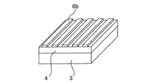
次に、本発明の第3実施形態による半導体発光素子の断面を図16に示し、発光層の形状を図17に示す。本実施形態の半導体発光素子はLEDであって、図1に示す第1実施形態のLEDにおいて、発光層6の複数の量子ドット6aを、図17に示すように、複数の量子細線6bに置き換えた構成となっている。そして、これらの量子細線6bからなる発光層6は、1層構造となっている。なお、本実施形態の半導体発光素子においても、量子細線6bの厚みおよび幅は、量子ドットの場合と同様の理由で、1nm〜100nmの範囲にあることが望ましい。量子細線の厚みおよび幅を1nm〜100nmの範囲にあることにより、量子ドットと同様に、キャリアの閉じ込めおよび量子準位の形成が生じ、複数の波長の発光を得ることができる。また、発光層6を構成する複数の量子細線は、厚みおよび幅は、それぞれの平均値の±5%の範囲内に半値幅が分布するように寸法制御される。すなわち、発光層6を構成する複数の量子細線は、実質的に均一な厚みおよび幅を有している。
(Third embodiment)
Next, FIG. 16 shows a cross section of the semiconductor light emitting device according to the third embodiment of the present invention, and FIG. 17 shows the shape of the light emitting layer. The semiconductor light emitting device of this embodiment is an LED, and in the LED of the first embodiment shown in FIG. 1, the plurality of
次に、本実施形態の半導体発光素子(LED)の具体的な構成を、図16を参照して説明する。本実施形態のLEDは、まず、厚さ300μmの(0001)面サファイア(Al2O3の結晶)からなり、表面及び裏面の両面が鏡面に研磨された単結晶基板1上に形成される。この単結晶基板1の表面に、GaNからなる膜厚20nmのバッファ層2と、Siが添加されたn形のGaNからなる膜厚4μmの電極層3と、Siが添加されたn形のAl0.1Ga0.9Nからなる膜厚0.5μmのクラッド層4と、が順次形成される。なお、単結晶基板1は、サファイアに限るものではなく、例えば、窒化ガリウム(GaN)、シリコン(Si)、ガリウム砒素(GaAs)、炭化シリコン(SiC)や、酸化亜鉛(ZnO)やリチウムガレート(LiGaO2)、ZrB2などの結晶から構成するようにしてもよい。
Next, a specific configuration of the semiconductor light emitting device (LED) of the present embodiment will be described with reference to FIG. The LED of the present embodiment is first formed on a
また、n型クラッド層4上には、活性層6が形成されている。活性層6は、In0.65Ga0.35Nの組成からなる複数の量子細線6bが同一平面に配列された構造の層であり、ここでは、細線幅は50nm、高さ4nmの大きさに形成されている。本実施形態においては、図17に示すように、量子細線6bは、延在する方向に直交する断面形状が矩形であるが、これに限るものではない。テーパが付いている形状であってもよい。また図17では、量子細線6bが等間隔で配列されているが、これに限るものではなく、各量子細線6bの間隔は、不均一な状態で配置されていてもよい。また、量子細線6bは、量子細線6bを構成するInGaNの薄い膜でつながった状態に形成されていても良い。なお、量子細線6bは、実質的に均一な寸法に形成されているものである。
An
このように複数の量子細線6bから構成された活性層6は、ノンドープのGaNからなる膜厚10nmの成長カバー層(バリア層)7により覆われている。この成長カバー層7上には、Mgが添加されたp型のAl0.1Ga0.9Nからなる膜厚0.5μmのp型クラッド層8と、Mgが添加されたp形のGaNからなる膜厚0.1μmのコンタクト層9が順次形成されている。
Thus, the
コンタクト層9上には、電流注入領域を制限するための直径20μm程度の略円形の開口を有するSiO2からなる電流制限絶縁層10が形成されている。この電流制限絶縁層10上には、上記開口を介してコンタクト層9に接触するp形金属電極11が形成されている。p形金属電極11は、コンタクト層9に直接接触する膜厚50nmのニッケル層と、このニッケル層上に形成された膜厚200nmの金層との積層構造となっている。
On the
なお、電極層3は、この電極層3上の各層を一部エッチングすることで形成された露出領域3aを有しており、この露出領域3aにn形金属電極12が形成されている。n形金属電極12は、露出領域3aに直接接触する膜厚50nmのアルミニウム層と膜厚200nmの金層との積層構造となっている。
The
本実施形態のLEDの駆動電流を変化させると、基底準位からの黄色の発光で中心波長が580nm、励起準位の(量子細線の高さ方向に直交する面内方向の閉じ込めにより形成された)第2準位からの緑色の発光で中心波長が540nm、さらに励起準位の(高さ方向の閉じ込めにより形成された)第2準位からの青色の発光で中心波長が485nmの光出力が得られた。また、量子細線の寸法により、半導体発光素子から出射される複数の光の発光波長が決定されることがわかった。 When the driving current of the LED of the present embodiment is changed, yellow light is emitted from the ground level, the center wavelength is 580 nm, and the excitation level is formed by confinement in the in-plane direction perpendicular to the height direction of the quantum wire. ) A green light emission from the second level with a center wavelength of 540 nm, and a blue light emission from the second level of the excitation level (formed by confinement in the height direction) with a central wavelength of 485 nm. Obtained. Further, it has been found that the emission wavelengths of a plurality of lights emitted from the semiconductor light emitting element are determined by the dimensions of the quantum wires.
(製造方法)
次に、本実施形態における半導体発光素子(LED)の製造方法について説明する。ここでは、結晶成長に関しては、第1実施形態で説明した製造工程と同様であるので、ここでは、量子細線6bの作製およびそれ以降の工程について述べる。第1実施形態との違いは、InGaNをドット状ではなく膜状に厚さ4nmで成長し、この膜に対して電子線描画リソグラフィ技術と塩素系ガスを用いた反応性イオンエッチングを行うことにより、細線幅50nm、周期100nmの周期溝構造を<1−100>方向に沿って形成した。
(Production method)
Next, a method for manufacturing a semiconductor light emitting device (LED) in the present embodiment will be described. Here, since crystal growth is the same as the manufacturing process described in the first embodiment, here, the fabrication of the
次いで、活性層6に対するエッチングやこの活性層の結晶性の劣化を抑制するために、窒素キャリアガスを用いてInGaNと同じ成長温度である500℃でGaNを成長し、細線構造を覆うように成長カバー層7を形成する。成長カバー層7は、InGaNからなる複数の量子細線6bに対するバリア層となる。成長カバー層7を形成した後、基板温度を1020℃に上昇させて成長カバー層7の高品質化を図る。
Next, in order to suppress etching of the
引き続いて、Mgが添加されたp形Al0.1Ga0.9N及びマグネシウムが添加されたp形GaNを順次成長させ、クラッド層8、コンタクト層9を形成する。Mgを添加するための原料としては、メチルカプタン・ビスシクロペンタ・ジエニルマグネシウム(MeCP2Mg)を用いる。この原料は液体であり、一般に用いられている固体原料であるビスシクロペンタ・ジエニルマグネシウム(Cp2Mg)より、Mgの添加濃度の再現性が良い。クラッド層8、コンタクト層9を形成した後、これらの層の添加したMgの活性化を図るために、700℃の窒素雰囲気中で30分間アニールする。
Subsequently, p-type Al 0.1 Ga 0.9 N to which Mg is added and p-type GaN to which magnesium is added are sequentially grown to form a
次に、上述した各結晶層を形成した後、RFマグネトロン・スパッタ装置を用い、コンタクト層9上にSiO2からなる電流制限絶縁層10を形成し、この電流制限絶縁層10を公知のフォトリソグラフィ技術とエッチング技術とによりパターニングし、開口を形成する。電流制限絶縁層10に開口を形成した後、電子ビーム蒸着装置を用い、開口内を含む電流制限絶縁層10の上に、膜厚50nmのニッケル,膜厚100nmの金を順に蒸着して積層し、p形金属電極11となる金属層を形成する。
Next, after forming each of the crystal layers described above, a current limiting insulating
この後、公知のフォトリソグラフィ技術により、上記金属層の上にポジ型フォトレジストのパターンを形成し、このパターンをマスクとして下層をエッチングし、電極層3に露出領域3aを形成する。このエッチングにおいて、例えば、結晶層のエッチングでは、塩素ガスを用いた反応性イオンエッチングにより行えばよい。上記露出領域3aを形成するエッチングを行い、フォトレジストのパターンを除去し、単結晶基板1及びこの上に形成した構造体をクリーニングした後、電極層3の露出領域3aに膜厚50nmのアルミニウム、膜厚200nmの金を順に蒸着してこれらをパターニングし、n型金属電極12を形成する。
Thereafter, a positive photoresist pattern is formed on the metal layer by a known photolithography technique, the lower layer is etched using this pattern as a mask, and an exposed
以上説明したことにより、n形金属電極12までを形成した後、これらを洗浄し、ダイヤモンド・スクライバを用いて単結晶基板1を所定の寸法に切断し、素子に切り出す。切り出した素子に所定の電流を印加して動作させれば、単結晶基板1の裏面側より発光光が得られる。
As described above, after forming up to the n-
また、第2実施形態の図9に示すレーザ構造の活性層6の量子ドット6aを量子細線6bに置き換えることによって、基底準位および励起準位からの複数の波長での発振が行われるレーザ素子を作製できる。
Further, a laser element that oscillates at a plurality of wavelengths from the ground level and the excitation level is obtained by replacing the
以上述べたように、本実施形態によれば、発光効率が高く、演色性が高い半導体発光素子を提供することができる。 As described above, according to this embodiment, it is possible to provide a semiconductor light emitting device with high luminous efficiency and high color rendering.
(第4実施形態)
次に、本発明の第4実施形態による半導体発光素子の断面を図18に示す。本実施形態の半導体発光素子は、図1に示す第1実施形態の半導体発光素子において、電極層3と、n型クラッド層4との間に多層膜からなる共振器20を設けた構成となっている。この共振器20を構成する多層膜はある特定波長に共振するように構成されているので、異なる量子準位からの複数の発光波長に対して、それぞれの発光スペクトルの狭帯域化する。
(Fourth embodiment)
Next, FIG. 18 shows a cross section of the semiconductor light emitting device according to the fourth embodiment of the present invention. The semiconductor light emitting device of this embodiment has a configuration in which a
本実施形態の半導体発光素子は、GaN基板1上に、GaNバッファ層2、n型GaNからなる電極層3、共振器20を構成する5対のAl0.3Ga0.7N層とGaN層との積層構造よりなる多層膜反射鏡、n型クラッド層4、活性層層6、成長カバー層7層、p型クラッド層8、コンタクト層9が順次積層されている。コンタクト層9上に、底部がコンタクト層9に到達する開口を備えた電流制限絶縁層10が形成され、この開口を埋め込むようにp型電極層11が形成されている。また、GaNからなる電極層3の露出領域3a上にn型電極12が形成されている。
In the semiconductor light emitting device of this embodiment, a
活性層6には複数の波長で発光強度のピークを有する発光源が設けられている。本実施形態おいては、活性層6からみてn型クラッド層4側に多層膜反射鏡20を設けているが、活性層6からみてp型クラッド層側に多層膜反射鏡層を設けて活性層6を含む共振器構造を設けてもよい。すなわち、多層膜反射鏡層は、活性層6からみて片側に設けてもよいし、両側に設けてもよい。
The
少なくとも一つの発光強度のピーク波長あるいはそのピークの一部での発光波長幅(スペクトル幅)を狭くすることで、各波長の分離を容易にする。活性層の発光源としては複数のサイズの量子ドットあるいは量子細線でもよく、単一のサイズの量子ドットあるいは量子細線であっても異なる準位を有しているものであっても良い。多層膜反射鏡としてはGaN層とGaAlN層とが積層された多層膜反射鏡でも、誘電体多層膜反射鏡でもよい。誘電体多層膜反射鏡としてはTiO2層とSiO2層との組み合わせでも、Ta2O3層とSiO2層との組み合わせのほか、誘電体と金属の組み合わせでもよい。 Separation of each wavelength is facilitated by narrowing the emission wavelength width (spectrum width) at the peak wavelength of at least one emission intensity or a part of the peak. The light emitting source of the active layer may be a plurality of sizes of quantum dots or quantum wires, or may be a single size of quantum dots or quantum wires having different levels. The multilayer mirror may be a multilayer mirror in which a GaN layer and a GaAlN layer are laminated, or a dielectric multilayer mirror. The dielectric multilayer reflector may be a combination of a TiO 2 layer and a SiO 2 layer, a combination of a Ta 2 O 3 layer and a SiO 2 layer, or a combination of a dielectric and a metal.
以上述べたように、本実施形態によれば、発光効率が高く、演色性が高い半導体発光素子を提供することができる。 As described above, according to this embodiment, it is possible to provide a semiconductor light emitting device with high luminous efficiency and high color rendering.
(第5実施形態)
次に、本発明の第5実施形態による半導体発光素子の断面を図19に示す。本実施形態の半導体発光素子は、n型の導電型のGaN基板1上にSi添加のn型GaNバッファ層2が形成されている。このバッファ層2上にGaNとAlGaNのペア構造を積層してなる多層膜反射鏡層31、GaNよりなるn型コンタクト層32、GaNからなるn型クラッド層33が積層されている。n型クラッド層33上に活性層40が設けられている。この活性層40は、Ga1−xInxN(0≦x≦1)からなる量子ドット36をGa1−yInyN(0≦y≦1、x>y)からなる埋め込み層37で埋め込んだ発光層38と、GaNからなる量子障壁層39とが3層に積層された構造となっている。
(Fifth embodiment)
Next, FIG. 19 shows a cross section of the semiconductor light emitting device according to the fifth embodiment of the present invention. In the semiconductor light emitting device of this embodiment, an Si-doped n-type
活性層40上に、GaNからなる第一クラッド層41、p型AlGaNからなる第二クラッド層42、p型GaNからなるコンタクト層43が積層されている。そして、コンタクト層43上にITOからなるp型透明導電層44が形成され、この透明導電層44上にSiO2膜とTiO2膜とを積層してなる誘電体多層膜反射鏡層45が形成されている。
A
更に、全体に二段のメサ構造46a、46bが形成されており、メサ構造46a、46bによりn型GaNからなるコンタクト層32と、ITOからなるp型透明電極層44との表面が露出されている。更に、全体にSiO2からなるパッシベーション膜47が被覆されている。このパッシベーション膜47に開口を設けることでGaNからなるn型コンタクト層32と、p型透明導電層44の表面が露出されて、それぞれの部分に対してAlからなるn型金属電極50と、AlNiからなるp型金属電極51が設けられている。
Further, two-
ここで、GaInNからなる量子ドット36の発光の強度ピークの波長をλ2とし、AlGaNとGaNを積層してなる多層膜反射鏡層31の各層の厚さは光路長として波長λ2のm/4(mは奇数)倍となるよう構成する。また、TiO2とSiO2よりなる誘電体多層膜反射鏡層45の各層も光路長でλ2のn/4(nは奇数)倍となるように構成する。更に、GaNコンタクト層32、GaNクラッド層33、活性層40、GaN第1クラッド層41、AlGaN第2クラッド層42、p型GaNコンタクト層43全体の光路長をλ2の整数倍とし、多層膜反射鏡層31の表面を低屈折率のAlGaN、誘電体多層膜反射鏡層45の活性層側を低屈折率のSiO2層とすることで、λ2に対してエタロン構造が形成され、λ2に対して狭線幅化が図れる。
Here, the wavelength of the emission intensity peak of the
本実施形態の光半導体素子は第1実施形態や第2実施形態と同様の方法で作製可能であり、誘電体多層膜に関しては、通常の電子線を用いた蒸着法や反応性蒸着法などを用いることができる。 The optical semiconductor device of this embodiment can be manufactured by the same method as that of the first and second embodiments. For the dielectric multilayer film, a vapor deposition method using a normal electron beam or a reactive vapor deposition method is used. Can be used.
GaInNからなる量子ドット36の基底準位の発光の強度ピークの波長をλ1として、第一励起準位の発光の強度ピークの波長をλ2として第三励起準位の発光強度のピーク波長をλ3とする。この場合、λ1、λ2、λ3の波長重なりが小さくなるので分離が容易に行える。例えば、λ1が赤色の600nm〜650nm帯での発光、λ2を560nm帯での発光、更にλ3を青色の470nmでの発光の関係を満たすように量子ドット36のサイズとInの組成を形成する。このように構成された本実施形態の半導体発光素子に注入する電流を変えた場合の特性を図20乃至図21を参照して説明する。図20に示すように注入する電流の大きさを増大させた場合、光出力も増大し、電流を(1)〜(7)のように増大すると、本実施形態の半導体発光素子の発光スペクトルは図21に示すように変化する。
The wavelength of the emission peak of the ground level of the
図21からわかるように、注入電流密度を変えることで、基底準位での赤色発光、第一励起準位での多層膜反射鏡により狭帯域化された緑色発光、第二励起準位での青色発光が逐次得られる。このような特性は量子ドット36の高さを7nm程度、Inの組成比を57%程度にすることで得られる。その横方向(高さと直交する方向)のサイズも量子ドット36の高さと同程度としてよい。
As can be seen from FIG. 21, by changing the injection current density, red emission at the ground level, green emission narrowed by the multilayer reflector at the first excitation level, and at the second excitation level. Blue light emission is obtained sequentially. Such characteristics can be obtained by setting the height of the
ここで、量子ドット36の横方向のサイズに関しては、断面が円形であれば直径として定義することができ、正方形であれば一辺の長さとするなど、底面の大きさを示す長さと考えることができる。このようにすると、どの方向の励起準位も同程度のエネルギーを持つので、中間のエネルギーで発光することがなく、高い効率で発光が得られる。
Here, the lateral size of the
以上述べたように、本実施形態によれば、発光効率が高く、演色性が高い半導体発光素子を提供することができる。 As described above, according to this embodiment, it is possible to provide a semiconductor light emitting device with high luminous efficiency and high color rendering.
(第6実施形態)
次に、本発明の第6実施様態による半導体発光素子を説明する。本実施形態の半導体発光素子は、多層膜反射鏡により量子ドットからの複数の波長の発光を狭線幅化して、各波長の光を分離するものであって、その構成は第5実施形態の半導体発光素子と概略同一であり、異なる点について説明する。
(Sixth embodiment)
Next, a semiconductor light emitting device according to a sixth embodiment of the present invention will be described. The semiconductor light emitting device of this embodiment narrows light emission of a plurality of wavelengths from a quantum dot by a multilayer reflector and separates light of each wavelength. The configuration is the same as that of the fifth embodiment. The difference between the semiconductor light emitting element and the semiconductor light emitting element will be described.
GaInN量子ドットの二つの準位からの発光強度のピークの波長λ1、λ2に対して、多層膜反射鏡の各層の光学膜厚dがd=λ1×(2m−1)/4=λ2×(2n−1)/4 (m,nは自然数、m<n)の関係を満たすと、多層膜反射鏡が波長λ1の光に対して高反射率の膜となる場合には、波長λ2の光に対しても高反射率の膜となる。このため、二つの光に対して同時に高反射率を有する膜を形成することができる。この点を利用してエタロンを形成することで、2種類の波長の比が2n−1と2m−1の狭線幅化した光を放射する光半導体素子を形成することができる。特に、二種類の波長の比がλ1:λ2=5:3またはλ1:λ2=7:5としたときにいずれも可視光の光を放出することができる。λ1/λ2がこれよりも大きい場合には一方は可視光で無くなる。λ1/λ2がこれより小さい場合には多層膜反射鏡の光学膜厚のn、mが大きくなりエタロンの特性が劣化するので、波長の選択性が劣化する。 The optical film thickness d of each layer of the multilayer reflector is d = λ1 × (2m−1) / 4 = λ2 × (with respect to the wavelengths λ1 and λ2 of the emission intensity peaks from the two levels of the GaInN quantum dots. 2n-1) / 4 (where m and n are natural numbers, m <n) When the multilayer mirror becomes a highly reflective film with respect to light with wavelength λ1, light with wavelength λ2 In contrast, the film has a high reflectivity. For this reason, it is possible to form a film having a high reflectance with respect to two lights at the same time. By using this point to form an etalon, it is possible to form an optical semiconductor element that emits light with a narrow linewidth having a ratio of two types of wavelengths of 2n-1 and 2m-1. In particular, visible light can be emitted when the ratio of the two wavelengths is λ1: λ2 = 5: 3 or λ1: λ2 = 7: 5. If λ1 / λ2 is larger than this, one is not visible light. When λ1 / λ2 is smaller than this, the optical film thicknesses n and m of the multilayer reflector are increased, and the characteristics of the etalon are degraded, so that the wavelength selectivity is degraded.
AlGaN層とGaN層とを積層してなる多層膜反射鏡層31の各層の光路長における厚さ(光学膜厚)は発光波長λ1の3/4倍または5/4倍とする。また、TIO2層とSiO2層よりなる誘電体多層膜反射鏡層45の各層の光路長おける厚さ(光学膜厚)も発光波長λ1の3/4倍または5/4倍とする。例えば、光学膜厚を青紫色の光の波長440nmの5/4倍である550nmとすると、赤色の光の波長733nmの3/4倍となる。ここで、GaInNからなる量子ドット36の基底準位の発光の強度ピークの波長をλ1とし、第一励起準位の発光の強度ピークの波長をλ2として、λ1:λ2=5:3または7:5の関係を満たすように量子ドット36のサイズとInの組成を形成することで、多層膜反射鏡層31と誘電体多層膜反射鏡層45がλ1の波長の光に対して高反射膜である場合にはλ2の波長の光に対しても高反射膜となる。
The thickness (optical film thickness) in the optical path length of each layer of the
更に、GaNからなるコンタクト層32、GaNからなるクラッド層33、活性層40、GaNからなる第一クラッド層41、AlGaNからなる第二クラッド層42、およびp型GaNからなるコンタクト層43の全体の光路長をλ1の3倍ないし5倍(つまりλ2の5倍ないし7倍)とし、多層膜反射鏡層31の表面を低屈折率のAlGaN、誘電体多層膜反射鏡層45の活性層側を低屈折率のSiO2層とすることで、λ1とλ2の二つの波長に対して同時にエタロン構造が形成される。
Further, the
このため、λ1とλ2の光が狭線幅化されて基底準位の光と第一励起準位の光のフィルタリングが行え、放出光の混同が起こらない。特にλ2を390nm〜560nmとしてλ1をその7/5倍の550nm〜780nmとすれば、λ1、λ2ともに可視光となるので、可視のLEDあるいはLDとしての2色光源を実現することができる。また、λ2を390nm〜470nmとして、λ1をその5/3倍である650nm〜780nmとすれば、2色が可視光の範囲内では最も多層膜反射鏡の性能を高くすることができ、エタロンの特性を最も高くすることができ、波長の混合のない光半導体素子を実現することができる。
For this reason, the light of λ1 and λ2 is narrowed so that the ground level light and the first excitation level light can be filtered, and the emitted light is not confused. In particular, when λ2 is 390 nm to 560 nm and λ1 is 7/5
このような条件を満たすためには、λ1とλ2の光のエネルギー差が(1240/λ2−1240/λ1)eVであり、λ1/λ2=7/5の場合には、0.62eV〜0.92eVとなり、λ1/λ2=5/3の場合には、1.05eV〜1.27eVとなる。これらの場合、それぞれ量子ドットの量子化エネルギーは0.2eV〜0.3eV、0.35eV〜0.4eV程度となる。これらの条件を考慮すると量子ドット36を構成するInGaNのInの組成比は0.65以上であることが望ましく、量子ドット36のサイズは2nm〜3nm程度となる。
In order to satisfy such a condition, the energy difference between the light beams of λ1 and λ2 is (1240 / λ2-1240 / λ1) eV, and when λ1 / λ2 = 7/5, 0.62 eV to 0. 92 eV, and in the case of λ1 / λ2 = 5/3, it is 1.05 eV to 1.27 eV. In these cases, the quantization energy of the quantum dots is about 0.2 eV to 0.3 eV and about 0.35 eV to 0.4 eV, respectively. Considering these conditions, the In composition ratio of InGaN constituting the
例えば、λ1/λ2=5/3として、λ2を440nm、λ1を730nmとする場合、Inの組成を77%、量子ドット36の高さを2.3nmとすればよい。また例えば、λ1/λ2=7/5として、λ2を470nm、λ1を660nmとする場合、Inの組成を65%、量子ドット36の高さを2.4nmとすればよい。また例えば、λ1/λ2=7/5として、λ2を550nm、λ1を770nmとする場合、Inの組成を73%、量子ドット36の高さを2.7nmとすればよい。
For example, when λ1 / λ2 = 5/3, λ2 is set to 440 nm, and λ1 is set to 730 nm, the composition of In may be 77%, and the height of the
量子ドット36の横方向の直径は高さと同等の2nm〜3nmとしてもよい。ここで、横方向に関しては側面が円形でなければ径を定義することはできないが、正方形であれば、一辺の長さとするなど、底面の大きさを示す長さと考えることができる。このようにするとどの方向の励起準位も同程度のエネルギーを持つので、中間のエネルギーで発光することがなく、高い効率で発光が得られる光半導体素子を実現することができる。
The lateral diameter of the
また、量子ドット36の高さを2nm〜3nmとして横方向の長さを10nm以上とすると、室温では横方向への閉じ込めが弱くなり、バンド間のエネルギー差が室温のエネルギーと大差なくなることから、量子ドット36の高さ方向の準位に対してサブバンド的に機能してエネルギー幅が広くなり、エタロンで定まる発光エネルギーに対して量子ドット36の高さのマージンが広くなり、実効的に高い発光効率を得ることができる。
Also, if the height of the
以上述べたように、本実施形態によれば、発光効率が高く、演色性が高い半導体発光素子を提供することができる。 As described above, according to this embodiment, it is possible to provide a semiconductor light emitting device with high luminous efficiency and high color rendering.
(第7実施形態)
次に、本発明の第7実施形態による半導体発光装置の概略断面を図22に示す。本実施形態の半導体発光装置は、図22に示すように、半導体発光素子61、62、63を備えている。これらの半導体発光素子61、62、63は、第1実施形態の発光素子であって、同一基板1上に設けられている。
(Seventh embodiment)
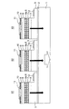
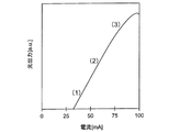
Next, FIG. 22 shows a schematic cross section of the semiconductor light emitting device according to the seventh embodiment of the present invention. The semiconductor light emitting device of this embodiment includes semiconductor
本実施形態の半導体発光装置の出力特性を図23に示す。図23に示すように、電流を増大した場合、光出力は増大する。そこで、本実施形態の半導体発光装置の発光素子61、62、63に図23に示す(1)、(2)、(3)の電流を流した場合の、本実施形態による半導体発光装置の発光スペクトルを図24に示す。図24からわかるように、本実施形態による半導体発光装置に(1)の電流を流した場合は波長が630nmの赤色光、(2)の電流を流した場合は波長が555nmの緑色光、(3)の電流を流した場合は波長が475nmの青色光がそれぞれ出力される。したがって、本実施形態の半導体発光装置の発光素子61に図23に示す(1)の電流を流した場合は発光素子61から波長が630nmの赤色光、発光素子62に図23に示す(2)の電流を流した場合は発光素子62から波長が555nmの緑色光、発光素子63に図23に示す(3)の電流を流した場合は発光素子63から波長が475nmの青色光が出力される。なお、本実施形態では、半導体発光素子61、62、63は、第1実施形態の発光素子であったが、第1実施形態の変形例および第2乃至第6実施形態の発光素子のいずれかであってもよい。
The output characteristics of the semiconductor light emitting device of this embodiment are shown in FIG. As shown in FIG. 23, when the current is increased, the light output increases. Therefore, the light emission of the semiconductor light emitting device according to the present embodiment when the currents (1), (2), and (3) shown in FIG. 23 are supplied to the
上述したように、量子ドット構造を持つ本実施形態の半導体発光装置による発光素子では、同一基板に形成した各発光素子に印加する駆動電流が異なる場合、異なる色の光を発光させることができる。このため、本実施形態の半導体発光装置は、照明装置に用いることができる。 As described above, in the light emitting element by the semiconductor light emitting device of this embodiment having the quantum dot structure, when the driving current applied to each light emitting element formed on the same substrate is different, light of different colors can be emitted. For this reason, the semiconductor light-emitting device of this embodiment can be used for an illuminating device.
現在、様々な照明、ディスプレイにおいて、色の3原色である、R、G、Bの各色をそれぞれ段階制御することにより、様々な色を再現している。色の再現性は、制御階調が豊富であるほどより自然な色表現が可能である。本実施形態においては、発光素子の駆動電流を変えることにより、様々な波長の光を制御することが可能であり、1024階調制御すれば10億色以上の色再現が可能である。 Currently, in various lighting and displays, various colors are reproduced by step-controlling each of R, G, and B, which are the three primary colors. As for the color reproducibility, the richer the control gradation, the more natural color expression is possible. In this embodiment, it is possible to control light of various wavelengths by changing the driving current of the light emitting element, and it is possible to reproduce more than 1 billion colors by controlling 1024 gradations.
従来の発光装置は、R、G、Bの各色の発光素子がそれぞれ異なる基板上に作製され、これらを寄せ集めることで作製されている。 In the conventional light emitting device, light emitting elements of each color of R, G, and B are manufactured on different substrates and are manufactured by gathering them together.
これに対して、本実施形態では、同一基板上に異なる発光素子を作製している。したがって、本実施形態の半導体発光装置では、各色の発光素子のピッチ間隔を小さくすることで高集積化および高精細化が図れるという利点を併せ持っている。このため、本実施形態の半導体発光装置は、発光素子はLEDの場合は、図22に示す3個の発光素子61、62、63を1画素とし、発光素子61、62、63がR、G、Bをそれぞれ表示するサブピクセルである平面表示装置として用いることができる。
In contrast, in the present embodiment, different light emitting elements are manufactured on the same substrate. Therefore, the semiconductor light emitting device of this embodiment has the advantage that high integration and high definition can be achieved by reducing the pitch interval between the light emitting elements of the respective colors. Therefore, in the semiconductor light emitting device of this embodiment, when the light emitting element is an LED, the three
また、本実施形態の半導体発光装置は、発光素子の長寿命化を図る上でも好適である。例えば、白色照明やLEDディスプレイなどに用いる場合、ある期間は発光素子61からR(赤)、発光素子62からG(緑)、発光素子63からB(青)を発光させ、またある期間は発光素子61からG、発光素子62からB、発光素子63からRを発光させ、またある期間は発光素子61からB、発光素子62からR、発光素子63からGを発光させるように印加する駆動電流を定期的に変えることにより、各発光素子61、62、63に掛かる負荷が均等化とすることが可能となるため、通常のデバイスに比べ長寿命化を図ることができる。
Further, the semiconductor light emitting device of this embodiment is also suitable for extending the life of the light emitting element. For example, when used for white illumination or an LED display, the
また、図22に示す同一基板上に作製した3個の発光素子61、62、63に対し、各発光素子の駆動する電流を変え、赤、緑、青の3色を同時に発生させることにより照明、ディスプレイ用の白色LEDおよびレーザを実現できることに加え、各発光素子を別々の信号により、それぞれ10Mbpsの速度で変調させ、受信側に、光学バンドパスフィルタなどを用いることで、3色それぞれのデータ通信を行うこともできる。すなわち、通信に本実施形態の半導体発光装置を用いれば、色多重化により伝送容量を増大させることができる。
In addition, for the three
本実施形態では、同一基板上に3個の発光素子を作製したが、2個の発光素子または4個以上の発光素子を同一基板上に形成しても、同様の効果が得られることとは明らかである。特に照明やディスプレイの応用では、同一基板上に高密度に集積化できるので、従来のデバイスに比べ非常に大きな利点がある。 In this embodiment, three light emitting elements are manufactured on the same substrate, but the same effect can be obtained even if two light emitting elements or four or more light emitting elements are formed on the same substrate. it is obvious. Especially in lighting and display applications, it can be integrated at a high density on the same substrate, which is a great advantage over conventional devices.
また、本実施形態では、駆動する電流値を変えることにより、3個の発光素子を用いて、赤、緑、青の3色で実証したが、これ以外の様々な色、波長において発光させることが可能であり、従来の発光素子よりも、照明の演色性、ディスプレイにおける色再現性、通信における情報量、伝送容量の増大が期待できる。なお、通信に用いる場合は可視光でなくともよいが、二種類の可視光を用いることにより、いずれの光を用いているときにも、信号の伝送が行われていることを容易に確認することができる。また、2種類の光が同時に放射されている場合(人間の認識において同時に放射されていると認識される場合)色の変化により、二種類の光を用いた通信が行われていることを確認できる。更に、表示デバイスと通信デバイスを兼用する場合、ディスプレイに点灯させたまま通信できる時間が長くなるので、通信をより長時間行えるようになる。 Also, in this embodiment, the three currents of red, green, and blue are demonstrated using three light emitting elements by changing the current value to drive, but light is emitted in various other colors and wavelengths. As compared with conventional light-emitting elements, it is possible to expect an increase in illumination color rendering, color reproducibility in display, information amount in communication, and transmission capacity. In addition, when using for communication, it does not have to be visible light, but by using two types of visible light, it is easy to confirm that signal transmission is being performed when using either light. be able to. Also, when two types of light are emitted at the same time (when recognized as being emitted simultaneously by human recognition), it is confirmed that communication using two types of light is being performed due to a color change it can. Furthermore, when the display device and the communication device are used together, the time during which communication can be performed while the display is lit is increased, so that communication can be performed for a longer time.
以上述べたように、本実施形態によれば、発光効率が高く、演色性が高く、高速通信が可能な半導体発光装置を提供することができる。 As described above, according to the present embodiment, it is possible to provide a semiconductor light emitting device that has high luminous efficiency, high color rendering properties, and capable of high-speed communication.
また、本発明の各実施形態によれば、長寿命で、製造しやすい可視光域の半導体発光素子および半導体発光装置を得ることができる。 Further, according to each embodiment of the present invention, it is possible to obtain a semiconductor light emitting device and a semiconductor light emitting device having a long lifetime and easy to manufacture in the visible light range.
また、本発明の一実施形態による白色発光素子は、基板上に形成され、発光層を含む窒化ガリウム系半導体発光素子において、発光層は、発光層は、周りの半導体の禁止帯幅(バンドギャップエネルギー)より小さい禁止帯幅を有する半導体材料の3次元量子構造である量子ドット構造を有し、量子ドットはその禁止帯幅および量子準位(励起準位)に対応した波長の光を発する。量子ドット構造は、形状、外径、高さがほぼ同一に揃った均一性の高い、その寸法に対応した波長の光を発する。量子ドットはバンドギャップエネルギーが周囲の半導体のバンドギャップエネルギーより小さく、そのキャリアが閉じ込められるので、高い発光効率で発光させることができる。発光波長は量子ドットの外径に対応する。すなわち、量子ドットにおいては、微小領域への閉じ込めにより、伝導帯や価電子帯の準位は離散化する。伝導帯、価電子帯の電子、正孔は、基底準位、第2準位などの完全に離散化された量子準位のみに局在することになる。量子ドットに電流を注入して発光させる際に、駆動電流値を変化させると基底準位、第二準位などからの発光が得られ、複数の波長での発光が得られる。 In addition, the white light emitting device according to an embodiment of the present invention is formed on a substrate and includes a light emitting layer. In the gallium nitride based semiconductor light emitting device, the light emitting layer has a band gap (band gap) of a surrounding semiconductor. The quantum dot has a quantum dot structure which is a three-dimensional quantum structure of a semiconductor material having a smaller band gap than (energy), and the quantum dot emits light having a wavelength corresponding to the band gap and the quantum level (excitation level). The quantum dot structure emits light having a wavelength corresponding to the dimension of the uniform, highly uniform shape, outer diameter, and height. The quantum dot has a band gap energy smaller than that of the surrounding semiconductor and its carriers are confined, so that it can emit light with high light emission efficiency. The emission wavelength corresponds to the outer diameter of the quantum dot. That is, in the quantum dot, the levels of the conduction band and the valence band are discretized by confinement in a minute region. Electrons and holes in the conduction band and valence band are localized only in completely discretized quantum levels such as the ground level and the second level. When injecting current into the quantum dots to emit light, if the drive current value is changed, light emission from the ground level, the second level, etc. is obtained, and light emission at a plurality of wavelengths is obtained.
上記のように、量子ドットの外径は同一でも、複数の量子準位からの発光は、それぞれ異なる波長となる。例えば、赤色光から青色光に渡る波長域の光を発光させ、これらを混合すれば、所望の白色光を得ることができる。したがって、高い演色性を確保することができる。量子ドットからの発光は、上述のように、非常に発光効率が高いことが知られており、優れた発光効率を得ることができる。また、蛍光材料のように寿命を制約する因子がないので、長寿命を得ることができる。上記量子ドットは、成膜条件の制御などにより自発的に自己形成されることが知られており、成膜条件を把握すれば製造は容易である。 As described above, even if the outer diameters of the quantum dots are the same, light emission from a plurality of quantum levels has different wavelengths. For example, desired white light can be obtained by emitting light in a wavelength range from red light to blue light and mixing them. Therefore, high color rendering properties can be ensured. As described above, light emission from quantum dots is known to have very high light emission efficiency, and excellent light emission efficiency can be obtained. Further, since there is no factor that limits the lifetime as in the fluorescent material, a long lifetime can be obtained. It is known that the quantum dots are spontaneously formed by controlling the film formation conditions and the like, and manufacturing is easy if the film formation conditions are grasped.
なお、上記量子ドットはTEM(Transmission Electron Microscopy)、カソードルミネッセンス、AFM(Atomic Force Microscopy)などにより容易に観察することができる。また、その他の市販のナノテクノロジ用の観察装置を用いて観察してもよい。この後で説明する量子細線についても同様である。 The quantum dots can be easily observed by TEM (Transmission Electron Microscopy), cathode luminescence, AFM (Atomic Force Microscopy), or the like. Moreover, you may observe using the observation apparatus for other commercially available nanotechnology. The same applies to the quantum wire described later.
本発明の他の実施形態による白色発光素子は、発光層を含む窒化ガリウム系半導体発光素子において、発光層は、周りの半導体の禁止帯幅より小さい禁止帯幅を有する線状半導体である量子細線を複数本含む。そして、複数本の量子細線の幅は、同一であり、各量子細線はその量子準位に対応した波長の光を発する。上記量子ドットがキャリアの閉じ込めによる高効率発光の零次元(点)とすると、上記構成における量子細線は、その1次元(線)といえる。このため、製造方法を除いて、上記量子ドットで述べた作用効果をそのまま引用することができる。製造方法については、基板を傾斜させるなどして成膜することにより量子細線を得ることができる。その他、これまでに既知の方法を適用することができる。上記の量子ドットおよび量子細線構造により、波長が単一ではなく複数の波長をもって発光するので、これら複数の波長の光を適宜混合することにより、優れた演色性を確保して、所望のトーンの白色を得ることができる。上記の波長対応寸法は、量子ドットの場合は外径寸法であり、量子細線の場合は細線の幅寸法である。 The white light emitting device according to another embodiment of the present invention is a gallium nitride based semiconductor light emitting device including a light emitting layer, wherein the light emitting layer is a linear semiconductor having a forbidden band width smaller than that of the surrounding semiconductor. Including a plurality. The plurality of quantum wires have the same width, and each quantum wire emits light having a wavelength corresponding to the quantum level. If the quantum dot is a zero-dimension (point) of high-efficiency light emission due to carrier confinement, the quantum wire in the above configuration can be said to be one-dimensional (line). For this reason, the effects described in the quantum dots can be cited as they are, except for the manufacturing method. As for the manufacturing method, quantum wires can be obtained by forming a film by tilting the substrate. In addition, known methods can be applied. The above-described quantum dot and quantum wire structure emit light with a plurality of wavelengths instead of a single wavelength. By appropriately mixing the light of the plurality of wavelengths, excellent color rendering properties can be ensured, and a desired tone can be obtained. A white color can be obtained. The wavelength-corresponding dimension is the outer diameter dimension in the case of quantum dots, and the width dimension of the thin lines in the case of quantum thin lines.
また、上記の複数の量子準位から発光する量子構造からなる活性層と共振器構造を組み合わせることにより、発光スペクトルの狭帯化を行う。これにより、複数の波長のそれぞれのスペクトルは重畳することなく発光される。また複数個のLEDが必要された白色発光素子において、本発明の素子では1個の発光素子により、白色発光を実現し、かつ色多重通信により伝送容量の増大が図れる。 In addition, the emission spectrum is narrowed by combining an active layer having a quantum structure emitting light from a plurality of quantum levels and a resonator structure. Thereby, each spectrum of a plurality of wavelengths is emitted without being superimposed. In addition, in a white light emitting element that requires a plurality of LEDs, the element of the present invention can realize white light emission by one light emitting element and increase transmission capacity by color multiplex communication.
上記の発光波長に対応する量子ドット、量子細線構造の寸法(サイズ)は、1nm以上100nm以下とすることができる。上記半導体の部分の寸法をこの寸法範囲内にすることにより、キャリア閉じ込めの量子効果を得ることができ、伝導帯や価電子帯の離散化による高い発光効率と、複数の発光波長を得ることができる。これら寸法は、上述のTEM、AFM、カソードルミネッセンス観察などを用いて測定することができる。また、上記の発光層は、p型およびn型窒化ガリウム系半導体によってはさまれるように配置するのがよい。この構成により、発光層にキャリアを注入することができ、外部からの入力により持続的な発光を行なうことができる。 The dimension (size) of the quantum dot and quantum wire structure corresponding to the above-described emission wavelength can be 1 nm or more and 100 nm or less. By making the size of the semiconductor portion within this size range, a quantum effect of carrier confinement can be obtained, and high emission efficiency and a plurality of emission wavelengths can be obtained by discretization of the conduction band and valence band. it can. These dimensions can be measured using the above-mentioned TEM, AFM, cathodoluminescence observation and the like. The light emitting layer is preferably arranged so as to be sandwiched between p-type and n-type gallium nitride semiconductors. With this configuration, carriers can be injected into the light emitting layer, and continuous light emission can be performed by an external input.
また、本発明の各実施形態の発光素子が形成される基板として、GaN、AlN、GaAs、Si、サファイア、SiC、ZnO、LiGaO2、ZrB2のうちのいずれかの材料を用いることができる。これらの基板は入手が容易であり、これら基板を用いてエピタキシャル成長した多層構造を形成することが可能となり、発光素子を製造することができる。 In addition, as a substrate on which the light emitting element of each embodiment of the present invention is formed, any material of GaN, AlN, GaAs, Si, sapphire, SiC, ZnO, LiGaO 2 , and ZrB 2 can be used. These substrates are easily available, and it becomes possible to form a multilayer structure epitaxially grown using these substrates, and a light emitting element can be manufactured.
1 基板
2 バッファ層
3 電極層
4 n型クラッド層
6 活性層層
6a 量子ドット
6b 量子細線
7 成長カバー層(バリア層)
8 p型クラッド層
9 コンタクト層
10 電流制限層
11 p型金属電極
12 n型金属電極
DESCRIPTION OF
8 p-
Claims (9)
前記第1半導体層上に設けられた第2導電型半導体からなる第2半導体層と、
前記第1半導体層と前記第2半導体層との間に設けられ、前記第1および第2半導体層の半導体の禁止帯幅より小さい禁止帯幅を有する半導体材料の複数の量子ドットを含み、駆動電流に応じて基底準位あるいは励起準位に対応した波長の光を発光する発光層と、
を備えたことを特徴とする半導体発光素子。 A first semiconductor layer made of a first conductivity type semiconductor provided on a substrate;
A second semiconductor layer made of a second conductivity type semiconductor provided on the first semiconductor layer;
Including a plurality of quantum dots of a semiconductor material provided between the first semiconductor layer and the second semiconductor layer and having a forbidden band width smaller than that of the semiconductor of the first and second semiconductor layers; A light emitting layer that emits light of a wavelength corresponding to a ground level or an excitation level according to an electric current;
A semiconductor light emitting device comprising:
前記第1半導体層上に設けられた第2導電型半導体からなる第2半導体層と、
前記第1半導体層と前記第2半導体層との間に設けられ、前記第1および第2半導体層の半導体の禁止帯幅より小さい禁止帯幅を有する半導体材料からなる実質的に均一な幅の複数の量子細線を含む発光層と、
を備えたことを特徴とする半導体発光素子。 A first semiconductor layer made of a first conductivity type semiconductor provided on a substrate;
A second semiconductor layer made of a second conductivity type semiconductor provided on the first semiconductor layer;
A substantially uniform width made of a semiconductor material provided between the first semiconductor layer and the second semiconductor layer and having a forbidden band width smaller than the forbidden band width of the semiconductor of the first and second semiconductor layers. A light emitting layer comprising a plurality of quantum wires;
A semiconductor light emitting device comprising:
前記第1半導体層上に設けられた第2導電型半導体からなる第2半導体層と、
前記第1半導体層と前記第2半導体層との間に設けられ、前記第1および第2半導体層の半導体の禁止帯幅より小さい禁止帯幅を有する半導体材料の複数の量子細線を含み、駆動電流に応じて基底準位あるいは励起準位に対応した波長の光を発光する発光層と、
を備えたことを特徴とする半導体発光素子。 A first semiconductor layer made of a first conductivity type semiconductor provided on a substrate;
A second semiconductor layer made of a second conductivity type semiconductor provided on the first semiconductor layer;
A plurality of quantum wires of a semiconductor material provided between the first semiconductor layer and the second semiconductor layer and having a forbidden band width smaller than that of the semiconductor of the first and second semiconductor layers; A light emitting layer that emits light of a wavelength corresponding to a ground level or an excitation level according to an electric current;
A semiconductor light emitting device comprising:
前記第1および第2半導体層の少なくとも一方の半導体層の前記発光層
とは反対側に設けられ、前記複数の波長の少なくとも一つの波長での発光波長の幅を狭くして各波長の分離が可能な多層膜反射鏡を更に備えたことを特徴とする請求項1乃至6のいずれかに記載の半導体発光素子。 The light emitting layer has a peak of light emission intensity at a plurality of wavelengths,
The at least one semiconductor layer of the first and second semiconductor layers is provided on the opposite side of the light emitting layer, and the width of the light emission wavelength at at least one of the plurality of wavelengths is narrowed to separate each wavelength. 7. The semiconductor light emitting device according to claim 1, further comprising a multilayer reflector that can be used.
Priority Applications (1)
| Application Number | Priority Date | Filing Date | Title |
|---|---|---|---|
| JP2005317038A JP2007123731A (en) | 2005-10-31 | 2005-10-31 | Semiconductor light emitting element and semiconductor light emitting device |
Applications Claiming Priority (1)
| Application Number | Priority Date | Filing Date | Title |
|---|---|---|---|
| JP2005317038A JP2007123731A (en) | 2005-10-31 | 2005-10-31 | Semiconductor light emitting element and semiconductor light emitting device |
Publications (1)
| Publication Number | Publication Date |
|---|---|
| JP2007123731A true JP2007123731A (en) | 2007-05-17 |
Family
ID=38147212
Family Applications (1)
| Application Number | Title | Priority Date | Filing Date |
|---|---|---|---|
| JP2005317038A Pending JP2007123731A (en) | 2005-10-31 | 2005-10-31 | Semiconductor light emitting element and semiconductor light emitting device |
Country Status (1)
| Country | Link |
|---|---|
| JP (1) | JP2007123731A (en) |
Cited By (27)
| Publication number | Priority date | Publication date | Assignee | Title |
|---|---|---|---|---|
| JPS5991535A (en) * | 1982-11-16 | 1984-05-26 | Matsushita Electric Ind Co Ltd | Setting switch of digital code |
| WO2007126092A1 (en) * | 2006-05-01 | 2007-11-08 | Mitsubishi Chemical Corporation | Integrated semiconductor light emitting device and method for manufacturing same |
| WO2008153120A1 (en) * | 2007-06-15 | 2008-12-18 | Rohm Co., Ltd. | White light-emitting device and method of forming white light-emitting device |
| WO2008155960A1 (en) * | 2007-06-15 | 2008-12-24 | Rohm Co., Ltd. | Semiconductor light-emitting device |
| JP2009054616A (en) * | 2007-08-23 | 2009-03-12 | Sharp Corp | Nitride semiconductor light emitting device manufacturing method and nitride semiconductor light emitting layer |
| CN101604717B (en) * | 2009-07-15 | 2010-12-29 | 山东华光光电子有限公司 | Vertical GaN-based LED chip and manufacture method thereof |
| CN101976800A (en) * | 2010-10-09 | 2011-02-16 | 吉林大学 | ZnO-based end surface emitting laser combined with ZnO and GaN and its preparation method |
| JP2011523206A (en) * | 2008-06-04 | 2011-08-04 | シャープ株式会社 | Nitride semiconductor devices |
| KR101081169B1 (en) | 2010-04-05 | 2011-11-07 | 엘지이노텍 주식회사 | Light emitting device and method for fabricating the same, light emitting device package, lighting system |
| JP2011238929A (en) * | 2010-05-10 | 2011-11-24 | Toshiba Corp | Semiconductor device and method of manufacturing semiconductor device |
| CN102263370A (en) * | 2010-10-09 | 2011-11-30 | 吉林大学 | p-ZnO and n-GaN combined multi-layer terminal emitting lasers and preparation methods |
| CN102263369A (en) * | 2010-10-09 | 2011-11-30 | 吉林大学 | p-ZnO and n-GaN combined ZnO-based terminal emitting lasers and preparation methods |
| JP2012044026A (en) * | 2010-08-20 | 2012-03-01 | Wakayama Univ | Optical semiconductor substrate, device for light source, and method of manufacturing optical semiconductor substrate |
| JP2012049337A (en) * | 2010-08-26 | 2012-03-08 | Sharp Corp | Nitride semiconductor element and semiconductor optical device |
| JP2013021377A (en) * | 2012-11-02 | 2013-01-31 | Toshiba Corp | Semiconductor light-emitting element |
| WO2013054431A1 (en) * | 2011-10-14 | 2013-04-18 | 富士通株式会社 | Semiconductor device, method for manufacturing same, and power supply apparatus |
| JP2014209609A (en) * | 2013-03-26 | 2014-11-06 | 京セラ株式会社 | Semiconductor laser |
| CN108878608A (en) * | 2018-06-01 | 2018-11-23 | 太原理工大学 | A kind of InGaN quantum dot LED epitaxial structure reducing structure with strain |
| CN109273566A (en) * | 2018-08-01 | 2019-01-25 | 太原理工大学 | Multilayer InGaN quantum dot structure containing strain modulation structure |
| CN109742249A (en) * | 2018-12-26 | 2019-05-10 | 深圳市华星光电半导体显示技术有限公司 | Quantum dot LED and manufacturing method thereof |
| US10355167B2 (en) * | 2015-11-20 | 2019-07-16 | Samsung Electronics Co., Ltd. | Light emitting device having nitride quantum dot and method of manufacturing the same |
| JP2021158268A (en) * | 2020-03-27 | 2021-10-07 | 株式会社デンソー | Semiconductor light emitting device |
| JP2022527622A (en) * | 2020-03-03 | 2022-06-02 | 東莞市中麒光電技術有限公司 | Light emitting diode and its manufacturing method |
| CN115461873A (en) * | 2020-04-28 | 2022-12-09 | 普列斯半导体有限公司 | Adjustable sub-pixel |
| JPWO2023032300A1 (en) * | 2021-08-30 | 2023-03-09 | ||
| WO2024225458A1 (en) * | 2023-04-28 | 2024-10-31 | 国立大学法人東京工業大学 | Single photon source device |
| WO2024237172A1 (en) * | 2023-05-17 | 2024-11-21 | ソニーグループ株式会社 | Light emitting device and electronic apparatus |
Citations (4)
| Publication number | Priority date | Publication date | Assignee | Title |
|---|---|---|---|---|
| JP2000330150A (en) * | 1999-05-20 | 2000-11-30 | Nec Corp | Semiconductor wavelength conversion element |
| US20040009681A1 (en) * | 2000-09-13 | 2004-01-15 | Simon Fafard | Quantum dot tunable external cavity laser (QD-TEC laser) |
| JP2004525498A (en) * | 2000-09-22 | 2004-08-19 | サイエンス アンド テクノロジー コーポレーション @ ユーエヌエム | Quantum dash device |
| JP2004528705A (en) * | 2000-10-06 | 2004-09-16 | サイエンス アンド テクノロジー コーポレーション @ ユーエヌエム | Quantum dot laser |
-
2005
- 2005-10-31 JP JP2005317038A patent/JP2007123731A/en active Pending
Patent Citations (4)
| Publication number | Priority date | Publication date | Assignee | Title |
|---|---|---|---|---|
| JP2000330150A (en) * | 1999-05-20 | 2000-11-30 | Nec Corp | Semiconductor wavelength conversion element |
| US20040009681A1 (en) * | 2000-09-13 | 2004-01-15 | Simon Fafard | Quantum dot tunable external cavity laser (QD-TEC laser) |
| JP2004525498A (en) * | 2000-09-22 | 2004-08-19 | サイエンス アンド テクノロジー コーポレーション @ ユーエヌエム | Quantum dash device |
| JP2004528705A (en) * | 2000-10-06 | 2004-09-16 | サイエンス アンド テクノロジー コーポレーション @ ユーエヌエム | Quantum dot laser |
Cited By (41)
| Publication number | Priority date | Publication date | Assignee | Title |
|---|---|---|---|---|
| JPS5991535A (en) * | 1982-11-16 | 1984-05-26 | Matsushita Electric Ind Co Ltd | Setting switch of digital code |
| WO2007126092A1 (en) * | 2006-05-01 | 2007-11-08 | Mitsubishi Chemical Corporation | Integrated semiconductor light emitting device and method for manufacturing same |
| WO2008153120A1 (en) * | 2007-06-15 | 2008-12-18 | Rohm Co., Ltd. | White light-emitting device and method of forming white light-emitting device |
| WO2008155960A1 (en) * | 2007-06-15 | 2008-12-24 | Rohm Co., Ltd. | Semiconductor light-emitting device |
| US8330181B2 (en) | 2007-06-15 | 2012-12-11 | Rohm Co., Ltd. | Semiconductor light-emitting device |
| JP5235878B2 (en) * | 2007-06-15 | 2013-07-10 | ローム株式会社 | Semiconductor light emitting device |
| JP2009054616A (en) * | 2007-08-23 | 2009-03-12 | Sharp Corp | Nitride semiconductor light emitting device manufacturing method and nitride semiconductor light emitting layer |
| JP2011523206A (en) * | 2008-06-04 | 2011-08-04 | シャープ株式会社 | Nitride semiconductor devices |
| CN101604717B (en) * | 2009-07-15 | 2010-12-29 | 山东华光光电子有限公司 | Vertical GaN-based LED chip and manufacture method thereof |
| US8878158B2 (en) | 2010-04-05 | 2014-11-04 | Lg Innotek Co., Ltd. | Light emitting device, light emitting device package, and lighting system |
| KR101081169B1 (en) | 2010-04-05 | 2011-11-07 | 엘지이노텍 주식회사 | Light emitting device and method for fabricating the same, light emitting device package, lighting system |
| JP2011238929A (en) * | 2010-05-10 | 2011-11-24 | Toshiba Corp | Semiconductor device and method of manufacturing semiconductor device |
| US8461569B2 (en) | 2010-05-10 | 2013-06-11 | Kabushiki Kaisha Toshiba | Semiconductor device and a method of fabricating a semiconductor device |
| JP2012044026A (en) * | 2010-08-20 | 2012-03-01 | Wakayama Univ | Optical semiconductor substrate, device for light source, and method of manufacturing optical semiconductor substrate |
| JP2012049337A (en) * | 2010-08-26 | 2012-03-08 | Sharp Corp | Nitride semiconductor element and semiconductor optical device |
| CN102263369B (en) * | 2010-10-09 | 2013-08-07 | 吉林大学 | p-ZnO and n-GaN combined ZnO-based terminal emitting lasers and preparation methods |
| CN102263370B (en) * | 2010-10-09 | 2013-07-10 | 吉林大学 | p-ZnO and n-GaN combined multi-layer terminal emitting lasers and preparation methods |
| CN102263369A (en) * | 2010-10-09 | 2011-11-30 | 吉林大学 | p-ZnO and n-GaN combined ZnO-based terminal emitting lasers and preparation methods |
| CN102263370A (en) * | 2010-10-09 | 2011-11-30 | 吉林大学 | p-ZnO and n-GaN combined multi-layer terminal emitting lasers and preparation methods |
| CN101976800A (en) * | 2010-10-09 | 2011-02-16 | 吉林大学 | ZnO-based end surface emitting laser combined with ZnO and GaN and its preparation method |
| US9231056B2 (en) | 2011-10-14 | 2016-01-05 | Fujitsu Limited | Semiconductor device and fabrication method therefor, and power supply apparatus |
| WO2013054431A1 (en) * | 2011-10-14 | 2013-04-18 | 富士通株式会社 | Semiconductor device, method for manufacturing same, and power supply apparatus |
| JP2013021377A (en) * | 2012-11-02 | 2013-01-31 | Toshiba Corp | Semiconductor light-emitting element |
| JP2014209609A (en) * | 2013-03-26 | 2014-11-06 | 京セラ株式会社 | Semiconductor laser |
| US10355167B2 (en) * | 2015-11-20 | 2019-07-16 | Samsung Electronics Co., Ltd. | Light emitting device having nitride quantum dot and method of manufacturing the same |
| CN108878608A (en) * | 2018-06-01 | 2018-11-23 | 太原理工大学 | A kind of InGaN quantum dot LED epitaxial structure reducing structure with strain |
| CN109273566B (en) * | 2018-08-01 | 2020-05-05 | 太原理工大学 | A Multilayer InGaN Quantum Dot Structure Containing a Strain Modulated Structure |
| CN109273566A (en) * | 2018-08-01 | 2019-01-25 | 太原理工大学 | Multilayer InGaN quantum dot structure containing strain modulation structure |
| CN109742249A (en) * | 2018-12-26 | 2019-05-10 | 深圳市华星光电半导体显示技术有限公司 | Quantum dot LED and manufacturing method thereof |
| JP7296482B2 (en) | 2020-03-03 | 2023-06-22 | 東莞市中麒光電技術有限公司 | Light emitting diode and manufacturing method thereof |
| JP2022527622A (en) * | 2020-03-03 | 2022-06-02 | 東莞市中麒光電技術有限公司 | Light emitting diode and its manufacturing method |
| JP7453649B2 (en) | 2020-03-27 | 2024-03-21 | 株式会社デンソー | semiconductor light emitting device |
| JP2021158268A (en) * | 2020-03-27 | 2021-10-07 | 株式会社デンソー | Semiconductor light emitting device |
| JP2023523354A (en) * | 2020-04-28 | 2023-06-02 | プレッシー・セミコンダクターズ・リミテッド | adjustable sub-pixel |
| CN115461873A (en) * | 2020-04-28 | 2022-12-09 | 普列斯半导体有限公司 | Adjustable sub-pixel |
| US12598888B2 (en) | 2020-04-28 | 2026-04-07 | Plessey Semiconductors Limited | Tuneable sub-pixel |
| JPWO2023032300A1 (en) * | 2021-08-30 | 2023-03-09 | ||
| WO2023032300A1 (en) * | 2021-08-30 | 2023-03-09 | ソニーグループ株式会社 | Light emitting device and image display device |
| JP7779320B2 (en) | 2021-08-30 | 2025-12-03 | ソニーグループ株式会社 | Light-emitting device and image display device |
| WO2024225458A1 (en) * | 2023-04-28 | 2024-10-31 | 国立大学法人東京工業大学 | Single photon source device |
| WO2024237172A1 (en) * | 2023-05-17 | 2024-11-21 | ソニーグループ株式会社 | Light emitting device and electronic apparatus |
Similar Documents
| Publication | Publication Date | Title |
|---|---|---|
| JP2007123731A (en) | Semiconductor light emitting element and semiconductor light emitting device | |
| KR100486803B1 (en) | Selfluminous display device | |
| US8399876B2 (en) | Semiconductor dies, light-emitting devices, methods of manufacturing and methods of generating multi-wavelength light | |
| CN101036237B (en) | Textured light emitting diodes | |
| KR100688239B1 (en) | Light emitting element | |
| KR101473288B1 (en) | Light-emitting diode display and method of producing the same | |
| KR100631040B1 (en) | Nitride semiconductor devices | |
| US7348600B2 (en) | Nitride semiconductor device, and its fabrication process | |
| JP4126751B2 (en) | Display device and lighting device | |
| KR101611412B1 (en) | Light emitting device | |
| KR101452801B1 (en) | Light emitting diode and method for manufacturing thereof | |
| WO2009041237A1 (en) | Iii nitride semiconductor light emitting element | |
| JP2780691B2 (en) | Nitride semiconductor light emitting device | |
| JP2002176198A (en) | Multi-wavelength light emitting device | |
| JP2012222362A (en) | Nitride semiconductor light-emitting element | |
| CN107004743B (en) | Semiconductor light-emitting element | |
| JP3470622B2 (en) | Nitride semiconductor light emitting device | |
| JP4770058B2 (en) | LIGHT EMITTING ELEMENT AND DEVICE | |
| KR102110446B1 (en) | Nanowire white light emitting diode and its fabrication method | |
| KR20220162167A (en) | Light emitting diode including an aluminum-containing layer therein and method related thereto | |
| KR20130040518A (en) | Semiconductor light emitting device and method for manufacturing the same | |
| JP2001237456A (en) | Light emitting element | |
| CN114078989A (en) | Full color light-emitting device | |
| JP3924973B2 (en) | Nitride semiconductor light emitting device manufacturing method and nitride semiconductor light emitting device | |
| JPH1093138A (en) | Display device with nitride semiconductor light emitting diode |
Legal Events
| Date | Code | Title | Description |
|---|---|---|---|
| A977 | Report on retrieval |
Free format text: JAPANESE INTERMEDIATE CODE: A971007 Effective date: 20100301 |
|
| A131 | Notification of reasons for refusal |
Free format text: JAPANESE INTERMEDIATE CODE: A131 Effective date: 20100305 |
|
| A02 | Decision of refusal |
Free format text: JAPANESE INTERMEDIATE CODE: A02 Effective date: 20100629 |