JP2007122017A - Phase plate, optical element, and image projection apparatus - Google Patents
Phase plate, optical element, and image projection apparatus Download PDFInfo
- Publication number
- JP2007122017A JP2007122017A JP2006212291A JP2006212291A JP2007122017A JP 2007122017 A JP2007122017 A JP 2007122017A JP 2006212291 A JP2006212291 A JP 2006212291A JP 2006212291 A JP2006212291 A JP 2006212291A JP 2007122017 A JP2007122017 A JP 2007122017A
- Authority
- JP
- Japan
- Prior art keywords
- phase plate
- light
- optical element
- optical
- thin layer
- Prior art date
- Legal status (The legal status is an assumption and is not a legal conclusion. Google has not performed a legal analysis and makes no representation as to the accuracy of the status listed.)
- Granted
Links
Images


Abstract
Description
この発明は、位相板・光学素子および画像投射装置に関する。 The present invention relates to a phase plate / optical element and an image projection apparatus.
光学素子の1種として知られる位相板は、互いに直交する偏光成分間に位相差を与える光学機能を持ち、種々の光学装置に用いられている。従来、位相板は、人造または天然の、ルチル、方解石、水晶など「複屈折性を示す一軸異方性結晶」を用いたものが知られているが、人造のものは「結晶を均一に成長させる」ことが難しく、天然の結晶は「光学的に均一で大きな形状のもの」が入手困難で高価である。また、このような「結晶材料を用いた位相板」は動作波長範囲が狭い。 A phase plate known as one type of optical element has an optical function of providing a phase difference between mutually orthogonal polarization components, and is used in various optical devices. Conventionally, phase plates using artificial or natural rutile, calcite, quartz and other “uniaxial anisotropic crystals exhibiting birefringence” are known, but artificial ones “grow crystals uniformly. Natural crystals are “optically uniform and large in shape” and are difficult to obtain and expensive. Such a “phase plate using a crystal material” has a narrow operating wavelength range.
近来「広帯域の波長範囲に対して機能できる位相板」として、サブ波長構造(SWS)による位相板が提案されている(特許文献1、2)。
サブ波長構造の光学作用に関しては非特許文献1等に説明がされている。また、サブ波長構造の形成方法の1例として非特許文献2記載のものが知られている。
Recently, a phase plate having a sub-wavelength structure (SWS) has been proposed as a “phase plate capable of functioning over a wide wavelength range” (
The optical action of the subwavelength structure is described in
特許文献1には、サブ波長構造を「ガラス基板の表面構造」として形成した位相板が開示されている。特許文献2には「平行平板を基板として平面状に格子構造を転写した位相板」が開示されているが、平行平板や格子構造を転写される部分の材質に関しては全く記載されていない。
非特許文献2には、サブ波長構造の形成方法として、樹脂バルク材を用いる熱式ナノインプリント方法が開示されている。この熱式ナノインプリント方法は、比較的容易にサブ波長構造を形成できるが、樹脂バルク材の1例としてPMMAを用いる場合を考えてみると、以下の如き問題がある。
Non-Patent
即ち、サブ波長構造により「互いに直交する偏光成分に対して与えられる位相差」は、サブ波長構造のアスペクト比に比例的であるため、例えば1/2波長の位相差を実現するためにはアスペクト比が10近くなり、樹脂が型の奥まで十分に入りにくく、正確なサブ波長構造を形成することが困難である。 That is, the “phase difference given to polarization components orthogonal to each other” by the sub-wavelength structure is proportional to the aspect ratio of the sub-wavelength structure. The ratio is close to 10, and it is difficult for the resin to enter the mold sufficiently, making it difficult to form an accurate subwavelength structure.
また、PMMAの樹脂バルクにエッチングでサブ波長構造を形成する場合にも、アスペクト比が大きいため、エッチング種が凹部の奥まで十分に入り込まず、形成される断面形状がテーパ状になり易い。即ち、サブ波長構造のピッチの微細さと高アスペクト比とは、トレードオフの関係にある。 Also, when the sub-wavelength structure is formed by etching in the resin bulk of PMMA, since the aspect ratio is large, the etching species do not sufficiently enter the depth of the recess, and the formed cross-sectional shape tends to be tapered. That is, the fine pitch of the sub-wavelength structure and the high aspect ratio are in a trade-off relationship.
この発明は、上述したところに鑑み、製造が容易で、広い波長帯域において位相板として良好な光学特性(透過率、リタデーションが略一定している)を有する新規な位相板、新規な光学素子、これらを用いる新規な画像投射装置の提供を課題とする。 In view of the above, this invention is a novel phase plate that is easy to manufacture and has good optical properties (transmittance, retardation is substantially constant) as a phase plate in a wide wavelength band, a novel optical element, It is an object of the present invention to provide a novel image projection apparatus using these.
この発明の位相板は、以下の如きものである(請求項1)。
即ち、ガラス平板の少なくとも一方の面に、屈折率:1.6以上の材料による薄層が形成され、該薄層の表面に「ランドとスペースによる断面矩形波状の微細凹凸構造」がサブ波長構造として形成されている。即ち、サブ波長構造は1次元的であって、1方向に凹凸構造を有し、その断面形状が矩形波状である。矩形波状は勿論「近似的な矩形波形状」の意味である。「ランドとスペース」については後述するが、簡単に言えば、「ランド」は微細凹凸構造における凸部に相当する部分であり、「スペース」は微細凹凸構造の凹部に相当する部分である。
The phase plate of the present invention is as follows (claim 1).
That is, a thin layer made of a material having a refractive index of 1.6 or more is formed on at least one surface of a glass flat plate, and “a fine concavo-convex structure having a rectangular wave section with lands and spaces” is formed on the surface of the thin layer. It is formed as. That is, the sub-wavelength structure is one-dimensional, has a concavo-convex structure in one direction, and has a rectangular wave shape in cross section. The rectangular wave shape naturally means “approximate rectangular wave shape”. Although “land and space” will be described later, simply speaking, “land” is a portion corresponding to a convex portion in the fine uneven structure, and “space” is a portion corresponding to a concave portion in the fine uneven structure.
また、断面矩形波状の微細凹凸構造が「サブ波長構造として形成」されているとは、微細凹凸構造をなす矩形波形状のピッチが使用波長(位相板として用いられるときの光の波長)より小さいことを意味するが、この発明の位相板は、広い波長領域において一定した光学特性を持つものであることから、この場合の使用波長は「上記波長領域の下限値」を意味する。 Further, the fact that the fine concavo-convex structure having a rectangular wave cross section is “formed as a sub-wavelength structure” means that the pitch of the rectangular wave shape forming the fine concavo-convex structure is smaller than the wavelength used (the wavelength of light when used as a phase plate). However, since the phase plate of the present invention has a constant optical characteristic in a wide wavelength region, the wavelength used in this case means “the lower limit value of the wavelength region”.
屈折率:1.6以上の材料による薄層は「ガラス平板の少なくとも一方の面」に形成されるから、ガラス平板の片面のみに形成されてもよいし、両面に形成されてもよい。ガラス平板は、両面が平行な「平行平板ガラス」でよいことは勿論であるが、断面が楔状の平板でもよい。ガラス平板の両面に薄層を形成する場合、各面に形成される薄層の材料は同一でも良いが、屈折率が1.6以上であることを条件として互いに異なっていても良い。 Since the thin layer made of a material having a refractive index of 1.6 or more is formed on “at least one surface of the glass flat plate”, it may be formed only on one surface of the glass flat plate or on both surfaces. The glass flat plate may be a “parallel flat plate glass” whose both surfaces are parallel, but may be a wedge-shaped flat plate. When forming a thin layer on both surfaces of a glass flat plate, the material of the thin layer formed on each surface may be the same, but may be different from each other on the condition that the refractive index is 1.6 or more.
請求項2記載の位相板は「微細凹凸構造のランドの幅がスペースの幅より広い」ことを特徴とする。
The phase plate according to
微細凹凸構造を特徴づけるパラメータとしてピッチ:Pやフリングファクタ:fがあるが、請求項2記載の位相板における「ランドの幅がスペースの幅より広い微細凹凸構造」は、微細凹凸構造のピッチ:P、フィリングファクタ:fが、条件:
(1) 0.1μm<P<0.4μm
(2) 0.5<f<0.8
を満足することが好ましい(請求項3)。
The parameters characterizing the fine concavo-convex structure include pitch: P and fling factor: f. The “fine concavo-convex structure in which the land width is wider than the space width” in the phase plate according to
(1) 0.1 μm <P <0.4 μm
(2) 0.5 <f <0.8
Is preferably satisfied (Claim 3).
請求項1〜3の任意の1に記載の位相板は、微細凹凸構造の上に反射防止膜を形成された構成であることができる(請求項4)。「微細凹凸構造の上に反射防止膜を形成された構成」とは、反射防止膜が微細凹凸構造の凸部の頂部と凹部の底部に形成された構成である。
The phase plate according to any one of
請求項1〜3の任意の1に記載の位相板はまた「微細凹凸構造のランドの上のみに反射防止膜を形成された構成」であることができる(請求項5)。「微細凹凸構造のランドの上のみに反射防止膜を形成された構成」とは、反射防止膜が「微細凹凸構造の凸部の頂部のみ」に形成された構成である。
The phase plate according to any one of
請求項6記載の光学素子は「プリズム機能やレンズ機能等の光学機能を持つ光学基体の平坦な面」に、請求項1〜5の任意の1に記載の位相板を一体化してなる。
請求項7記載の光学素子は「プリズム機能やレンズ機能等の光学機能を持つ光学基体の面に、屈折率:1.6以上の材料による薄層が形成され、この薄層の表面に「ランドとスペースによる断面矩形波状の微細凹凸構造」が形成され、この微細凹凸構造が光学基体に対して位相板として機能することを特徴とする。「薄層」は「光学機能を持つ光学基体の面」に形成されるので、光学基体の「薄層が形成される面」は平面に限らず、レンズ面等の曲面であってもよい。
The optical element according to
The optical element according to
請求項7記載の光学素子においても「微細凹凸構造におけるランドの幅がスペースの幅より広いことが好ましく(請求項8)、この場合においても、微細凹凸構造のピッチ:P、フィリングファクタ:fは、上記の条件(1)、(2)を満足することが好ましい。
請求項7または8記載の光学素子においても「薄層における微細凹凸構造の上に反射防止膜が形成された構成」とすることができ(請求項9)、また、薄層における微細凹凸構造の「ランド、即ち、凸部の上にのみ反射防止膜が形成された構成」とすることもできる(請求項10)。
Also in the optical element according to
Also in the optical element according to
請求項6〜10の任意の1に記載の光学素子は、その光学基体が、入射光を偏光面が互いに直交する反射光と透過光に分割する偏光分離面と、上記反射光と透過光のうちの一方を反射して他方の進行方向と略同じ方向に向ける反射面とを有し、略同方向に揃った透過光と反射光が射出する面側に、屈折率:1.6以上の材料による薄層が配置され、この薄層にサブ波長構造として形成されたランドトスペースによる断面矩形波状の微細凹凸構造が、反射光と透過光のうちの少なくとも一方の偏光面を変化させて双方の偏光面を一致させる位相板としての機能を有する構成とすることができる(請求項11)。
The optical element according to any one of
即ち、屈折率:1.6以上の材料による薄層は、光学基体の「略同方向に揃った透過光および反射光が射出する面」上に直接的に形成配置されてもよいし、請求項1〜5の何れかに記載の位相板の、ガラス平板の片面もしくは両面に形成され、位相板として上記「略同方向に揃った透過光および反射光が射出する面」に接着等の一体化手段で一体化されて配置されてもよい。光学基体の「略同方向に揃った透過光および反射光が射出する面」の上に薄層を直接的に形成する場合には、「略同方向に揃った透過光および反射光が射出する面」は平面でなく、レンズ面のように曲面であっても良い。
That is, a thin layer made of a material having a refractive index of 1.6 or more may be directly formed and disposed on the “surface on which transmitted light and reflected light that are aligned in substantially the same direction are emitted” of the optical substrate. The phase plate according to any one of
請求項12記載の画像投射装置は、光源からの光束を液晶表示素子に導光し、液晶表示素子の表示画像を投射レンズで表示面上に投射する画像投射装置であって、請求項1〜5の任意の1に記載の位相板、及び/または、請求項6〜11の任意の1に記載の光学素子が用いられたことを特徴とする。「表示面」は通常、スクリーンである。
An image projection apparatus according to
請求項12記載の画像投射装置は、3原色に対応し各色の映像を個別に形成する3つの液晶表示素子と、これら各液晶表示素子から射出した各色の映像光を合成するクロスプリズムを有し、各液晶表示素子とクロスプリズムとの間の3光路の1以上に「1/2波長板相当の位相板」として、請求項1〜5の任意の1に記載の位相板、または、請求項6〜10の任意の1に記載の光学素子を配置した構成とすることができる(請求項13)。
The image projection apparatus according to
請求項13記載の画像投射装置はまた、3原色に対応し各色の映像を個別に形成する3つの反射型液晶表示素子と、これら各反射型液晶表示素子から射出した各色の映像光を合成するクロスプリズムを有し、各反射型液晶表示素子とクロスプリズムとの間の3光路の1以上に「1/4波長板相当の位相板」として、請求項1〜5の任意の1に記載の位相板、または、請求項6〜10の任意の1に記載の光学素子を配置した構成とすることができる(請求項14)。
上記請求項13または14記載の画像投射装置は「光源からの光を直線偏光に揃える光学素子」として請求項11記載の光学素子を有することができる(請求項15)。
The image projection apparatus according to claim 13 also synthesizes three reflective liquid crystal display elements that individually form images of each color corresponding to the three primary colors, and video light of each color emitted from each of the reflective liquid crystal display elements. 6. The apparatus according to
The image projection apparatus according to the thirteenth or fourteenth aspect can include the optical element according to the eleventh aspect as "an optical element that aligns light from a light source with linearly polarized light" (claim 15).
薄膜を形成する「屈折率:1.6以上の材料」としては、TiO2,Nb2O5,Ta2O5,ZrO2、ITO(SnO2+In2O5)などの「無機材料」や、TiO2、ZrO2、Sb2O5、ITO、Al2O3等の元素を材料中に結合させた「ゾル・ゲル材料」、さらには、SiO2を骨格とするゾル・ゲル材料中に、上記無機材料の微粒子(5nm以上100nm以下)を分散させた「混合材料」、あるいは、光硬化型樹脂や熱硬化型樹脂で屈折率が1.6以上のもの等が利用可能である。上記混合材料は、特性に応じて混合・ブレンドが可能である。光硬化型樹脂や熱硬化型樹脂は、例えば、光透過型接着剤を初めとする「光学特性に優れたもの」が用いられる。 “Inorganic materials” such as TiO 2 , Nb 2 O 5 , Ta 2 O 5 , ZrO 2 , ITO (SnO 2 + In 2 O 5 ), etc. , TiO 2 , ZrO 2 , Sb 2 O 5 , ITO, Al 2 O 3, etc. are combined in the “sol-gel material”, and further, in the sol-gel material having SiO 2 as a skeleton A “mixed material” in which fine particles (5 nm to 100 nm) of the inorganic material are dispersed, or a photo-curing resin or a thermosetting resin having a refractive index of 1.6 or more can be used. The mixed material can be mixed and blended according to the characteristics. As the photocurable resin or thermosetting resin, for example, “excellent optical characteristics” including a light transmitting adhesive is used.
上記無機材料はスパッタリングや蒸着等の成膜技術で薄層を形成する。ゾル・ゲル材料や混合材料、光硬化型樹脂や熱硬化型樹脂は、ガラス平板上にスピンコート等で薄層を形成する。「無機材料による薄層」は200℃以上の耐熱性があり、高温環境で使用する位相板や光学素子の薄層として適している。 The inorganic material forms a thin layer by a film forming technique such as sputtering or vapor deposition. A sol / gel material, a mixed material, a photocurable resin, or a thermosetting resin forms a thin layer on a glass plate by spin coating or the like. The “thin layer made of an inorganic material” has a heat resistance of 200 ° C. or higher and is suitable as a thin layer for a phase plate or an optical element used in a high temperature environment.
なお、ランドとスペースによる微細凹凸構造は、例えば、薄層の上に「電子ビームの走査により潜像の形成されるレジスト層」を形成し、このレジストに「微細凹凸構造に対応するパターン」を電子ビームにより描画して潜像を形成し、これを現像して「微細凹凸構造に対応するレジストパターン」を得、このレジストパターンをマスクとしてRIE(反応性イオンエッチング)等のエッチングで「薄層を所望の溝深さにエッチングする」ことによって形成することができる。 The fine concavo-convex structure formed by lands and spaces is formed, for example, by forming a “resist layer on which a latent image is formed by scanning an electron beam” on a thin layer, and forming a “pattern corresponding to the fine concavo-convex structure” on this resist. A latent image is formed by drawing with an electron beam and developed to obtain a “resist pattern corresponding to a fine concavo-convex structure”. By using this resist pattern as a mask, etching such as RIE (reactive ion etching) is used to form a “thin layer Is etched to a desired groove depth ".
また、薄層を熱硬化性樹脂で構成した場合は、非特許文献2に記載された熱式ナノインプリント方法で形成することもできる。
Further, when the thin layer is composed of a thermosetting resin, it can be formed by a thermal nanoimprint method described in
上に説明したように、この発明の位相板や光学素子は、サブ波長構造として構成される薄層が「屈折率:1.6以上の材料」で構成されるため、透過光に与えられる位相差を大きくしても、微細凹凸構造のアスペクト比が過大にならず、製造容易である。特に、平行平板状のガラス平板の両面に「屈折率:1.6以上の材料により微細凹凸構造を有する薄層」を形成する場合、各面の薄層に形成する微細凹凸構造のアスペクト比は、片面にのみ形成する場合よりも更に小さくすることができる。 As described above, in the phase plate and optical element of the present invention, since the thin layer configured as the sub-wavelength structure is configured of “a material having a refractive index of 1.6 or more”, the phase plate or the optical element is provided with a level that can be given to transmitted light. Even if the phase difference is increased, the aspect ratio of the fine concavo-convex structure does not become excessive, and manufacturing is easy. In particular, when forming a “thin layer having a fine concavo-convex structure with a material having a refractive index of 1.6 or more” on both surfaces of a parallel flat glass plate, the aspect ratio of the fine concavo-convex structure formed on the thin layer on each surface is Further, it can be made smaller than when it is formed only on one side.
後述する実施例のように、この発明の位相板や光学素子における薄層は、広い波長領域にわたって、透過率やリタデーションが一定している。 As in the examples described later, the transmittance and retardation of the thin layer in the phase plate and optical element of the present invention are constant over a wide wavelength region.
この発明の光学素子は、光学基体自体がレンズ機能やプリズム機能あるいは、請求項11記載の如き光学機能を有するが、これらの光学機能と位相板としての機能とを組み合わせて複合的な光学機能を実現できる。
In the optical element of the present invention, the optical substrate itself has a lens function, a prism function, or an optical function as set forth in
この発明の位相板や光学素子を用いることにより、良好な画像投射機能を持った画像投射装置を実現できる。 By using the phase plate and optical element of the present invention, an image projection apparatus having a good image projection function can be realized.
以下、発明の実施の形態を説明する。
図1は、位相板の実施の1形態を説明するための図である。
この実施の形態の位相板は、図1(a)に示すように、平行平板状のガラス平板11の両面に薄層12a、12bが形成された構成となっている。
薄層12a、12bは屈折率:1.6以上の材料により形成され、その表面形状として「ランドとスペースによる断面矩形波状の微細凹凸構造」がサブ波長構造として形成されている。
Embodiments of the invention will be described below.
FIG. 1 is a diagram for explaining one embodiment of a phase plate.
The phase plate of this embodiment has a configuration in which
The
ここで、以下の説明のため、図1(b)を参照して用語を説明する。
図1(b)は薄層に形成された「断面矩形波状の微細凹凸構造」を説明図的に示している。微細凹凸構造の凹凸は断面形状が「矩形波形状」であり、このような矩形波状の凹凸が、図面に直交する方向へ均一な断面形状で形成されている。従って、微細凹凸構造における凸部は図面に直交する方向に長い「凸条」をなし、凹部は図面に直交する方向に長い「凹条」をなす。凸条をなす凸部を「ランド」と呼び、凹条をなす凹部を「スペース」と呼ぶのである。
Here, for the following explanation, terms will be explained with reference to FIG.
FIG. 1B schematically illustrates a “fine concavo-convex structure having a rectangular wave shape in cross section” formed in a thin layer. The unevenness of the fine unevenness structure has a “rectangular wave shape” in cross-sectional shape, and such rectangular wave-like unevenness is formed in a uniform cross-sectional shape in a direction orthogonal to the drawing. Accordingly, the convex portion in the fine concavo-convex structure forms a long “projection” in a direction orthogonal to the drawing, and the concave portion forms a long “concave” in a direction orthogonal to the drawing. The convex portion forming the ridge is called “land”, and the concave portion forming the ridge is called “space”.
断面矩形波状の微細凹凸構造のピッチ:Pは、図に示すように、1対をなすランドとスペースのランドの幅(以下、図示の如く「ランド幅」という。):aとスペースの幅(以下、図示の如く「スペース幅」という。):bの和:(a+b)である。また、スペース底部に対するランドの高さを「溝深さ:H」とする。 As shown in the figure, the pitch P of the fine concavo-convex structure having a rectangular wave cross section is a pair of land and space land width (hereinafter referred to as “land width” as shown): a and space width ( Hereinafter, it is referred to as “space width” as shown in the drawing): sum of b: (a + b). The height of the land with respect to the bottom of the space is defined as “groove depth: H”.
このとき、フィリングファクタは「a/P」、アスペクト比は「H/a」である。即ち「フィリングファクタが大きい」ことは、ピッチ:Pに占めるランド幅:aが大きい(スペース幅:bが小さい)ことを意味し、「アスペクト比が大きい」ほど、ランド幅:aに対する溝深さ:Hが大きい。アスペクト比は、微細凹凸構造形成の容易さの観点から「10よりも小さい」こと、より好ましくは、5程度以下が良い。 At this time, the filling factor is “a / P” and the aspect ratio is “H / a”. That is, “the filling factor is large” means that the land width: a occupying the pitch: P is large (the space width: b is small). As the “aspect ratio is large”, the groove depth with respect to the land width: a. : H is large. The aspect ratio is preferably “less than 10”, more preferably about 5 or less, from the viewpoint of easy formation of a fine relief structure.
非特許文献1、2等により知られたように、微細凹凸構造がサブ波長構造であると、そのピッチよりも大きい波長の光は回折せず「0次光」としてそのまま透過する(このときの透過率を「0次透過率」と呼ぶ。)が、入射光に対して複屈折性を示す。
As known from
即ち、図1(c)に示すように、微細凹凸構造へ「空気領域から入射」する入射光において、微細凹凸構造の周期方向(図の左右方向)に平行に振動する偏光成分:TM、ランド長手方向(図面に直交する方向)に平行に振動する偏光成分:TEに対し、微細凹凸構造は「屈折率が異なる媒質」のように作用する。 That is, as shown in FIG. 1C, in the incident light “incident from the air region” to the fine concavo-convex structure, polarization components that vibrate in parallel to the periodic direction (left-right direction in the figure) of the fine concavo-convex structure: TM, land The fine concavo-convex structure acts like a “medium having a different refractive index” with respect to a polarized light component TE that vibrates parallel to the longitudinal direction (direction orthogonal to the drawing).
微細凹凸構造の部分における有効屈折率を、偏光成分:TMにつきn(TM)、偏光成分:TEについてn(TE)とすると、これらの有効屈折率は、微細凹凸構造が形成された薄層の材料の屈折率:n、微細凹凸構造のフィリングファクタ:fを用いて以下のように表される。
n(TE)=√{fn2+(1−f)} (1)
n(TM)=√[n2/{f+(1−f)n2}] (2)
このため、透過光における偏光成分:TMに対し、偏光成分:TEは、図1(c)に示すように位相が「δ」だけ遅れることになる。
Assuming that the effective refractive index in the fine concavo-convex structure portion is n (TM) for the polarization component: TM and n (TE) for the polarization component: TE, these effective refractive indexes are the values of the thin layer on which the fine concavo-convex structure is formed. It is expressed as follows using the refractive index of the material: n and the filling factor of the fine relief structure: f.
n (TE) = √ {fn 2 + (1−f)} (1)
n (TM) = √ [n 2 / {f + (1−f) n 2 }] (2)
For this reason, the phase of the polarization component TE in the transmitted light is delayed by “δ” as shown in FIG.
即ち、溝深さ:Hを用いると、微細凹凸構造の「光学的厚さ」は、偏光成分:TMに対して「H・n(TM)」、偏光成分:TEに対して「H・n(TE)」であるので、これら光学的厚さの差:H{n(TE)−n(TM)}に応じて「位相遅れ:δ」が生ずる。この「位相遅れ:δ」が「リタデーション」である。
光学的厚さの差:H{n(TE)−n(TM)}をDとし、波長をλとすると、δ=2πD/λであるが、微細凹凸構造においては「波長:λの広い領域にわたって、略一定のリタデーション」が得られる。
That is, when the groove depth: H is used, the “optical thickness” of the fine concavo-convex structure is “H · n (TM)” for the polarization component: TM and “H · n” for the polarization component: TE. (TE) ", a“ phase delay: δ ”is generated according to the difference in optical thickness: H {n (TE) −n (TM)}. This “phase delay: δ” is “retardation”.
Difference in optical thickness: where H {n (TE) −n (TM)} is D and wavelength is λ, δ = 2πD / λ, but in the fine concavo-convex structure, “wavelength: wide region of λ” A substantially constant retardation "is obtained.
n(TE)、n(TM)は、薄層の材料の屈折率:nと、フィリングファクタ:fにより決定され、リタデーション:δは、屈折率:n、フィリングファクタ:f、溝深さ:Hにより定まるから、結局、リタデーションは薄層の材料(nが定まる。)と微細凹凸構造の形態(フィリングファクタ:fと溝深さ:Hが定まる。)を調整することにより所望のものを得ることができる。 n (TE) and n (TM) are determined by the refractive index of the thin layer material: n and the filling factor: f. Retardation: δ is the refractive index: n, the filling factor: f, and the groove depth: H. As a result, retardation can be obtained by adjusting the material of the thin layer (n is determined) and the form of the fine concavo-convex structure (filling factor: f and groove depth: H are determined). Can do.
図1(a)に示す実施の形態のように、ガラス平板11の両面に微細凹凸構造が形成されている場合、微細凹凸構造12aによるリタデーションを「δ1」、微細凹凸構造12bによるリタデーション「δ2」とすれば、位相板としてのリタデーションは「δ1+δ2」となる。
When fine concavo-convex structures are formed on both surfaces of the glass
従って、図1(a)に示す位相板の場合には、リタデーション:δ1+δ2を調整することにより、偏光成分:TM、TEに対する位相差を、例えば「πやπ/2」に設定でき、各種波長板を実現できる。 Therefore, in the case of the phase plate shown in FIG. 1A, by adjusting the retardation: δ1 + δ2, the phase difference with respect to the polarization components TM, TE can be set to, for example, “π or π / 2”, and various wavelengths can be set. A board can be realized.
図2は、薄層に形成された微細凹凸構造により「所望のリタデーション(例えば「π/2」)」を実現するための「薄層材料の屈折率とアスペクト比との関係」を示している。所望のリタデーションを実現するのに「薄層材料の屈折率:nが小さいほど、アスペクト比を大きくする必要がある」ことが分かる。 FIG. 2 shows a “relation between the refractive index of the thin layer material and the aspect ratio” for realizing “desired retardation (eg,“ π / 2 ”)” by the fine uneven structure formed in the thin layer. . It can be seen that, in order to realize the desired retardation, “the smaller the refractive index of the thin layer material: n, the larger the aspect ratio is required”.
微細凹凸構造形成の容易性から前述の如くアスペクト比を10以下とすると、薄層材料の屈折率は1.6以上であること必要である。即ち、請求項1において薄層材料の屈折率を1.6以上とするのは、アスペクト比を10以下とし、微細凹凸構造の形成を容易にする(所望のピッチ:P、フィリングファクタ:f、溝深さ:Hをもった微細凹凸構造を確実に形成できる)ための条件である。
If the aspect ratio is 10 or less as described above, the refractive index of the thin layer material needs to be 1.6 or more because of the ease of forming the fine uneven structure. That is, in
図2に示す場合において、アスペクト比を「より好ましい5程度以下」とするには、屈折率:2.0以上の薄層材料が必要である。 In the case shown in FIG. 2, a thin layer material having a refractive index of 2.0 or more is required to set the aspect ratio to “more preferably about 5 or less”.
図3は、薄層材料の屈折率:nとフィリングファクタ:fとをパラメータとし、溝深さH(横軸:μm単位)とリタデーション:δ(縦軸:波長単位)との関係を示している。溝深さ:Hの増大と共にリタデーション:δが線形に増加することがわかる。
これは、微細凹凸構造の「光学的厚さ」の、偏光成分:TM、TEに対する差:H{n(TE)−n(TM)}が溝深さ:Hの1次関数であることによる。
FIG. 3 shows the relationship between the groove depth H (horizontal axis: μm unit) and retardation: δ (vertical axis: wavelength unit) with the refractive index: n and the filling factor: f as parameters. Yes. It can be seen that the retardation: δ increases linearly as the groove depth: H increases.
This is because the difference between the “optical thickness” of the fine concavo-convex structure with respect to the polarization components: TM and TE: H {n (TE) −n (TM)} is a linear function of the groove depth: H. .
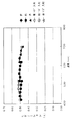
図4は、微細凹凸構造のピッチ:Pをパラメータとしたときの、「微細凹凸構造への入射光の偏光方向(単位:度)」と「0次透過率」との関係を示している。このときの薄層材料の屈折率:n=2.25である。 FIG. 4 shows the relationship between the “polarization direction (unit: degree) of incident light on the fine concavo-convex structure” and the “0th-order transmittance” when the pitch P of the fine concavo-convex structure is used as a parameter. The refractive index of the thin layer material at this time is n = 2.25.
微細凹凸構造を有する光学素子としての位相板を光学特性の面から見ると、0次透過率が大きく「入射光の偏光方向に対する依存性が小さい」ことが好ましい。このような、光学機能としての好ましい特性を「入射光の偏光方向の範囲:−180度〜+180度の範囲において、0次透過率:0.8以上」としてみると、図4から、ピッチは0.4以下であるべきことが分かる。 When a phase plate as an optical element having a fine concavo-convex structure is viewed from the viewpoint of optical characteristics, it is preferable that the 0th-order transmittance is large and “the dependency on the polarization direction of incident light is small”. When such a preferable characteristic as an optical function is assumed to be “the range of the polarization direction of incident light: in the range of −180 degrees to +180 degrees, 0th-order transmittance: 0.8 or more”, from FIG. It can be seen that it should be 0.4 or less.
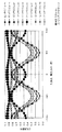
図5は、薄層材料の屈折率:n=2.29(波長:420nm)、2.23(波長:470nm)、2.20(波長:520nm)、2.17(波長:570nm)、2.16(波長:620nm)、2.14(波長:700nm)とし、微細凹凸構造における溝深さ:H=1μm、フィリングファクタ:f=0.7において、ピッチ:Pをパラメータとして変化させたとき、リタデーション:δが波長と共にどのように変化するかを示す図である。広い波長領域でリタデーションが安定した位相板であるためには、横軸の波長範囲において「リタデーションの変化が小さく略一定」であることが望まれる。 FIG. 5 shows the refractive index of the thin layer material: n = 2.29 (wavelength: 420 nm), 2.23 (wavelength: 470 nm), 2.20 (wavelength: 520 nm), 2.17 (wavelength: 570 nm), 2 .16 (wavelength: 620 nm), 2.14 (wavelength: 700 nm), when the groove depth in the fine relief structure is H = 1 μm, the filling factor is f = 0.7, and the pitch is changed with P as a parameter Retardation: how δ varies with wavelength. In order to provide a phase plate with stable retardation in a wide wavelength region, it is desired that “a change in retardation is small and substantially constant” in the wavelength range of the horizontal axis.
この条件を満足するのは、パラメータであるピッチ:Pが0.2〜0.4の範囲にある場合である。 This condition is satisfied when the parameter pitch: P is in the range of 0.2 to 0.4.
従って、先に述べた、ピッチ:Pとフィリングファクタ:fに対する条件(1)を満足することにより「広い波長範囲で略一定したリタデーションを有する位相板」が得られることが分かる。 Therefore, it is understood that “a phase plate having a substantially constant retardation in a wide wavelength range” can be obtained by satisfying the condition (1) for the pitch: P and the filling factor: f described above.
図6は、屈折率:n=2.29(波長:420nm)、2.23(波長:470nm)、2.20(波長:520nm)、2.17(波長:570nm)、2.16(波長:620nm)、2.14(波長:700nm)の薄層に、ピッチ:P=0.3μm、溝深さ:H=1μmで形成された微細凹凸構造に入射させる光の波長:λをパラメータとし、420nm、470nm、520nmに変化させたとき(図6(a))、520nm、570nm、620nmに変化させたとき、および(図6(b))と620nm、700nmに変化させたとき(図6(c))の、フィリングファクタ(横軸)とリタデーション(波長単位 縦軸)の関係を示している。 6 shows refractive indexes: n = 2.29 (wavelength: 420 nm), 2.23 (wavelength: 470 nm), 2.20 (wavelength: 520 nm), 2.17 (wavelength: 570 nm), 2.16 (wavelength). : 620 nm), 2.14 (wavelength: 700 nm) on a thin layer with a pitch: P = 0.3 μm and a groove depth: H = 1 μm. , 420 nm, 470 nm, and 520 nm (FIG. 6A), when changed to 520 nm, 570 nm, and 620 nm, and when changed to 620 nm and 700 nm (FIG. 6B). (C)) shows the relationship between the filling factor (horizontal axis) and retardation (vertical unit of vertical axis).
使用波長の領域を420nm〜700nmとした場合を想定し、この波長領域の入射光に対して略同一と見做し得るリタデーション(リタデーション変動:Δδ<±10%)を得るには、フィリングファクタの範囲として、0.5〜0.8の範囲(図6(a)〜図6(c)において破線で囲った範囲)が好適である。即ち、
0.5<f<0.8
であり、これが条件(2)の意義である。
Assuming that the wavelength region used is 420 nm to 700 nm, in order to obtain a retardation (retardation variation: Δδ <± 10%) that can be regarded as substantially the same with respect to incident light in this wavelength region, the filling factor of A range of 0.5 to 0.8 (a range surrounded by a broken line in FIGS. 6A to 6C) is preferable. That is,
0.5 <f <0.8
This is the significance of the condition (2).
条件(1)、(2)を満足することにより、入射光の偏光方向の範囲:±180度、0次透過率:80%で、リタデーション変動:Δδ<±10%の位相板を実現できる。 By satisfying the conditions (1) and (2), it is possible to realize a phase plate with retardation variation: Δδ <± 10% in the range of polarization direction of incident light: ± 180 degrees, zero-order transmittance: 80%.
この発明の位相板における薄層の材料は屈折率が1.6以上と高い。このため、微細凹凸構造に接する空気との屈折率差が大きいため、薄層表面での反射が大きくなりやすい。 The material of the thin layer in the phase plate of the present invention has a high refractive index of 1.6 or more. For this reason, since the refractive index difference with the air in contact with the fine concavo-convex structure is large, reflection on the surface of the thin layer tends to be large.
請求項4記載の位相板のように、微細凹凸構造の上に反射防止膜を形成することにより、薄層表面での反射を抑えることが好ましい。
図7は、このように反射防止膜を形成した実施の形態を説明するための図である。
図7(a)に示す薄層70は、屈折率:n=2.25の材料で形成され、微細凹凸構造はピッチ:P=0.22μm、溝深さ:H=1.086μm、フィリングファクタ:f=0.7のものである。微細凹凸構造70の上、即ち、微細凹凸構造70のランドの上とスペースの底部に反射防止膜71が形成されている。
As in the phase plate according to
FIG. 7 is a view for explaining an embodiment in which an antireflection film is formed in this way.
The
反射防止膜71は4層構造であり、図7(b)に示されたように、薄層側から数えて第1層が屈折率:2.35、厚さ:76nmの「高屈折率層」、第2層が屈折率:1.46、厚さ:7nmの「低屈折率層」、第3層が屈折率:2.35、厚さ:18nmの「高屈折率層」、第4層が屈折率:1.46、厚さ:78nmの「低屈折率層」である。
図16(a)は、反射防止膜を形成しない場合の偏光成分:TE(図16において「TE方向」)の0次透過率である。「R」は赤色波長領域、「G」は緑色波長領域、「B」は青色波長領域である。凡例に示すとおり、入射角を0度、5度、10度、15度としている。入射角:0度のときには、波長:480nm以下では「0次透過率が80%以下」になってしまっている。図16(b)は偏光成分:TM(図16において「TM方向」)の0次透過率である。
The
FIG. 16A shows the zero-order transmittance of the polarization component: TE (“TE direction” in FIG. 16) when no antireflection film is formed. “R” is a red wavelength region, “G” is a green wavelength region, and “B” is a blue wavelength region. As shown in the legend, the incident angles are 0 degrees, 5 degrees, 10 degrees, and 15 degrees. When the incident angle is 0 degree, the wavelength is 480 nm or less, and the 0th-order transmittance is 80% or less. FIG. 16B shows the zero-order transmittance of the polarization component: TM (“TM direction” in FIG. 16).
図16(a)、(b)の各場合につき、微細凹凸構造の上に上記図7(b)に構成を示す反射防止膜(図において「ARコート」)を形成した場合の、偏光成分:TEの0次透過率を図16(c)に、偏光成分:TMの0次透過率を16(d)に示す。 In each case of FIGS. 16A and 16B, the polarization component when the antireflection film (“AR coating” in the drawing) having the configuration shown in FIG. 7B is formed on the fine concavo-convex structure: FIG. 16C shows the zero-order transmittance of TE, and FIG. 16D shows the zero-order transmittance of the polarization component: TM.
図16(c)、(d)に示すように、0次透過率は偏光成分:TE、TMとも、波長:420nmから波長:700nmの範囲(B〜Rの波長領域)で88%以上となる。
なお、図16(a)、(b)では、符号R、G、Bで示す、各色波長領域の各短波長側に、0次透過率が低下する場合が「ひげ状」に存在するが、この部分は「1次回折光」により0次透過率が低下している箇所である。0次透過率の低下する「ひげ状の部分」は、図16(c)でも、B、Gの波長領域の各短波長側に存在し、図16(d)でも、Bの波長領域の短波長側に若干存在するが、このような「1次回折光が発生してない領域」については、図16(c)、(d)において「略99%以上の高0次透過率」を確保できている。
As shown in FIGS. 16 (c) and 16 (d), the zero-order transmittance is 88% or more in the range of wavelength: 420 nm to wavelength: 700 nm (B to R wavelength region) for both polarization components: TE and TM. .
In FIGS. 16A and 16B, there are cases where the 0th-order transmittance decreases in a “whisker shape” on each short wavelength side of each color wavelength region indicated by reference characters R, G, and B. This portion is where the 0th order transmittance is reduced by the “first order diffracted light”. The “whisker-shaped portion” in which the 0th-order transmittance decreases exists in each short wavelength side of the B and G wavelength regions in FIG. 16C, and also in FIG. Although slightly present on the wavelength side, “a high zero-order transmittance of about 99% or more” can be secured in FIGS. 16C and 16D for such “region where no first-order diffracted light is generated”. ing.
図16(c)、(d)は、反射防止膜を、図7に示すように微細工凸構造のランドとスペースとに設けた場合であるが、反射防止膜を「ランドの上のみ」に設けることによっても上記と同様の効果を得ることができる。 FIGS. 16C and 16D show the case where the antireflection film is provided on the land and the space of the fine convex structure as shown in FIG. 7, but the antireflection film is “only on the land”. The effect similar to the above can be acquired also by providing.
即ち、図17(c)、(d)は、上に説明したのと同じ反射防止膜を、ランドの上のみに形成した場合における偏光成分:TE、TM(図17においてTE方向、TM方向)の0次透過率を示す図で、図17(a)、(b)は図16(c)、(d)と同一である。 That is, FIGS. 17C and 17D show polarization components: TE and TM (TE direction and TM direction in FIG. 17) when the same antireflection film as described above is formed only on the land. FIGS. 17A and 17B are the same as FIGS. 16C and 16D.
図17の(a)と(c)、(b)と(d)とを比較すれば明らかなように、偏光成分:TE、TMの0次透過率は、反射防止膜をランドの上のみに形成した場合でも(反射防止膜をランドとスペースに形成した場合に比して、やや劣るが)88%以上の0次透過率を確保できている。 As is clear from comparison between FIGS. 17A and 17C and FIGS. 17B and 17D, the zero-order transmittance of the polarization components: TE and TM is that the antireflection film is placed only on the land. Even when it is formed (although slightly inferior to the case where the antireflection film is formed on the land and the space), the zero-order transmittance of 88% or more can be secured.
図18は「反射防止膜を形成することによる位相差への影響」を説明するための図である。図18(a)は「微細凹凸構造」を説明図的に示す図である。ピッチ:P=0.2μm、フィリングファクタ:f=0.8、溝深さ:H=0.3μm、屈折率:2.15の構造とした場合であり、波長:λ=660nmの光を入射させたときに発生するリタデーションは0.11λである。 FIG. 18 is a diagram for explaining “the influence on the phase difference caused by the formation of the antireflection film”. FIG. 18A is a diagram illustratively showing the “fine concavo-convex structure”. Pitch: P = 0.2 μm, Filling factor: f = 0.8, Groove depth: H = 0.3 μm, Refractive index: 2.15. Light having wavelength: λ = 660 nm is incident. Retardation generated when this is done is 0.11λ.
図18(b)は反射防止膜を説明する図であり、屈折率:2.15の平行平板の表面に、図の如く、空気側から屈折率:1.4で厚さ:100nmの第1層、屈折率:2.3で厚さ:30nmの第2層、屈折率:1.4で厚さ:10nmの第3層、屈折率:2.3で厚さ:80nmの第4層からなる4層構造で、ピッチ:P=0.2μm、フィリングファクタ:f=0.8の反射防止膜を形成した状態を示す。この反射防止膜に波長:λ=660nmの光を入射させたときに発生するリタデーションは0.02λである。 FIG. 18B is a diagram for explaining the antireflection film. As shown in the figure, the first antireflective film having a refractive index of 1.4 and a thickness of 100 nm is formed on the surface of a parallel plate having a refractive index of 2.15 from the air side. Layer, refractive index: 2.3, thickness: 30 nm, second layer, refractive index: 1.4, thickness: 10 nm, third layer, refractive index: 2.3, thickness: 80 nm In this four-layer structure, an antireflection film having a pitch: P = 0.2 μm and a filling factor: f = 0.8 is formed. The retardation generated when light having a wavelength of λ = 660 nm is incident on the antireflection film is 0.02λ.
図18(c)は、図18(a)に示した微細凹凸構造のランドの上のみに(b)に即して説明した4層構造の反射防止膜を形成した場合であり、このとき上記と同様に波長:λ=660nmの光を入射させた場合のリタデーションは0.19λとなる。 FIG. 18C shows a case where the antireflection film having the four-layer structure described in conformity with FIG. 18B is formed only on the land having the fine concavo-convex structure shown in FIG. In the same manner as described above, the retardation when light having a wavelength of λ = 660 nm is incident is 0.19λ.
図18(d)は、図18(a)に示す微細凹凸構造のランドとスペースとに、18(b)に即して説明した4層構造の反射防止膜を形成した場合であり、波長:λ=660nmの光を入射させた場合のリタデーションは0.12λである。ランドとスペースとに反射防止膜を形成する図18(d)の場合に比して、ランドの上のみに反射防止膜を形成する図18(c)の場合の方が、リタデーションを大きくすることが可能である。 FIG. 18D shows a case where the antireflection film having the four-layer structure described in accordance with 18B is formed on the land and space having the fine concavo-convex structure shown in FIG. Retardation when λ = 660 nm light is incident is 0.12λ. In the case of FIG. 18C in which the antireflection film is formed only on the land, the retardation is increased as compared with the case of FIG. 18D in which the antireflection film is formed on the land and the space. Is possible.
このように、反射防止膜はランドの上にのみ形成しても反射防止機能が発現し、高0次透過率を確保しつつ、リタデーションを大きくすることが可能である。なお、このような「ランドの上のみに反射防止機能を形成する構成」は、非特許文献1や2に掲載されている他のサブ波長構造の素子(偏光選択性の回折素子や、ある特定の波長域のみ光を透過させるフィルタなど)に関しても同様に反射防止機能を確保することが可能である。
As described above, even when the antireflection film is formed only on the land, an antireflection function is exhibited, and it is possible to increase the retardation while ensuring a high zero-order transmittance. In addition, such a “configuration for forming an antireflection function only on a land” refers to other sub-wavelength structure elements (polarization-selective diffractive elements or certain specific ones) described in
また、ランドの上のみに反射防止機能を形成する方法としては、上記の「高屈折率の薄層」で微細凹凸構造を形成したのちに、スペースに一旦「仮の部材」を充填して反射防止膜を蒸着し、その後「充填した部材とともにスペース上の仮の部材に蒸着されている反射防止膜」を除去する方法などを用いればよい。 In addition, as a method of forming an antireflection function only on the land, after forming a fine concavo-convex structure with the above-mentioned “high refractive index thin layer”, the space is once filled with a “temporary member” for reflection. A method of depositing an anti-reflection film and then removing the “anti-reflection film deposited on the temporary member in the space together with the filled member” may be used.
以下、画像投射装置の実施の形態を説明する。
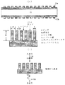
図8は、請求項13、14記載の画像投射装置の実施の1形態を示し、3原色に対応する各色の映像を個別に形成する3つの液晶表示素子110、111、112と、これら各液晶表示素子から射出した各色の映像光を合成するクロスプリズム113を有し、各液晶表示素子とクロスプリズム113との間の3光路に、1/2波長板相当の位相板116、117、118を有している。
白色光源101から放射された白色光はリフレクタ102により反射され、ダイクロイックミラー103に入射する。ダイクロイックミラー103は、青色波長以下の光を透過させ、青色波長より長い波長の光を反射する。従って、ダイクロイックミラー103に入射する白色光の内、青色成分はダイクロイックミラー103を透過し、緑色成分と赤色成分はダイクロイックミラー103により反射されてダイクロイックミラー104に入射する。
Hereinafter, embodiments of the image projection apparatus will be described.
FIG. 8 shows an embodiment of the image projection apparatus according to
White light emitted from the
ダイクロイックミラー104は赤色波長以上の波長の光を透過させ、赤色波長より短い波長の光を反射する。従って、ダイクロイックミラー104に入射した光のうち、緑色成分はダイクロイックミラー104に反射され、赤色成分はダイクロイックミラー104を透過する。このようにして、ダイクロイックミラー103、104により白色光源101からの白色光が、赤、緑、青の3原色の成分光に色分解される。
The
ダイクロイックミラー103を透過した「青色成分光」は、ミラー105により反射され、液晶表示素子110に入射し、ダイクロイックミラー104に反射された「緑色成分光」は、液晶表示素子111に入射する。また、ダイクロイックミラー104を透過した「赤色成分光」は、リレーレンズ108、ミラー106、リレーレンズ109、ミラー107により構成される光路を辿って液晶表示素子112に入射する。リレーレンズ108と109とは、赤色成分光の光路長補正を行う。
The “blue component light” transmitted through the
液晶表示素子110、111、112は「液晶層を1対の偏光子で挟持」してなり、液晶層を挟持する1対の偏光子は互いに偏光方向を直交させている。
各色成分光は、対応する液晶表示素子の入射側偏光子を透過すると直線偏光となって液晶層に入射する。液晶表示素子110、111、112にはそれぞれ、青色画像、緑色画像、赤色画像を表示するように画像信号が印加され、「投射すべき映像の画素」の位置の液晶層を透過する光は偏光面が90度旋回し、射出側偏光子と同じ偏光方向になって射出側偏光子を透過する。
The liquid
Each color component light becomes linearly polarized light and enters the liquid crystal layer when passing through the incident side polarizer of the corresponding liquid crystal display element. Image signals are applied to the liquid
このようにして、液晶表示素子110からは「青色画像に応じて2次元的に強度変調された青色成分光(以下「青色映像光」という。)」が射出する。同様に、液晶表示素子111からは「緑色画像に応じて2次元的に強度変調された緑色成分光(以下「緑色映像光」という。)」が射出し、液晶表示素子112からは「赤色画像に応じて2次元的に強度変調された赤色成分光(以下「赤色映像光」という。)」が射出する。即ち、液晶表示素子110、111、112は、3原色(青、緑、青)に対応する映像を個別に形成する。
In this way, the liquid
これら各液晶表示素子から射出した各色映像光は、その偏光方向が図面の面内に平行な方向となっている。
液晶表示素子110から射出した青色映像光は位相板116に入射し、液晶表示素子111、112からそれぞれ射出した緑色映像光、赤色映像光は、それぞれ位相板117、118に入射する。
Each color image light emitted from each liquid crystal display element has a polarization direction parallel to the plane of the drawing.
Blue video light emitted from the liquid
位相板116、117、118は「1/2波長板相当」であって、透過する光の直交2成分に対して1/2波長分の位相差を与える。これら位相板に入射する各色映像光は、上記の如く図面に平行な面内に偏光しているから、透過光はその偏光面が入射時の方向から90度旋回し、図面に直交する方向に偏光した光束となって、クロスプリズム113に、それぞれ対応する面から入射する。
The
クロスプリズム113は、図面に直交する方向からみた断面形状が正方形となる光透過性素材による直方体であり、互いに直交する反射面113a,113bを有している。反射面113aは「青色波長以下の波長の光を反射し、青色波長より長い波長の光を透過するダイクロイックミラー」となっており、反射面113bは「赤色波長以上の波長の光を反射し、赤色波長より短い波長の光を透過するダイクロイックミラー」となっている。
The
反射面113a、113bは、その「反射光の偏光軸」について方向性を有する。反射面113aは、青色波長以下の光のうち図面に直交する偏光成分の光(青色映像光)を良好に反射させるが、図面に直交する偏光成分の緑色映像光・赤色映像光は良好に透過させる。反射面113bは、図面に直交する偏光成分の赤色映像光を良好に反射させ、図面に直交する偏光成分の青色映像光と緑色映像光は良好に透過させる。
The reflecting
クロスプリズム113に入射する各色映像光のうち、青色映像光は反射面113aに反射され、赤色映像光は反射面113bに反射され、緑色映像光は反射面113a、113bを透過し、いずれも同一の方向となり、色合成されてクロスプリズム113から射出する。射出した光束は投射レンズ114に入射し、投射レンズ114により「表示面」であるスクリーン115上に拡大投射されて投射映像を表示する。
Of the color image lights incident on the
図9は、図8に示した実施の形態の変形例である。繁雑を避けるため、混同の恐れが無いと思われるものについては図8におけると同一の符号を付し、これらについての説明は図8に関する説明を援用する。 FIG. 9 is a modification of the embodiment shown in FIG. In order to avoid confusion, the same reference numerals as those in FIG. 8 are given to those which are not likely to be confused, and the description of FIG.
図9の画像投射装置は、図8の画像投射装置に対し、白色光源101とダイクロイックミラー103との間に、均一照明手段201(オプチカルインテグレータ)と偏光変換素子202とを付加したものである。
The image projection apparatus in FIG. 9 is obtained by adding a uniform illumination means 201 (optical integrator) and a
「オプチカルインテグレータ」である均一照明手段201は、液晶表示素子への照射光の光量を略均一にする手段であり、例えばフライアイレンズ、ロッドレンズ、矩形レンズアレイ等から成る公知のものを適宜利用できる。 The uniform illumination means 201, which is an “optical integrator”, is a means for making the amount of light irradiated to the liquid crystal display element substantially uniform. For example, a well-known device composed of, for example, a fly-eye lens, a rod lens, a rectangular lens array, or the like is appropriately used. it can.
偏光変換素子202は、白色光源101からの光を有効に使い、スクリーン上の投射映像を明るくするために液晶表示素子へ入射する光の偏光方向を揃えるのに用いられる。
The
液晶表示素子110、111、112は、液晶の持つ偏光特性を利用しており、高いコントラストを実現できるが、1対の偏光子で液晶を挟持しているため、図8に示した実施の形態におけるように「各液晶表示素子に入射する照射光が自然偏光状態である」と、各液晶表示素子の「入射側偏光子」を透過する際に、照明光量の1/2が遮断されてしまうことになり、光の利用効率が悪い。
The liquid
偏光変換素子202は、光源側からの照明光の偏光状態を「照明光の光強度を略保存しつつ、自然偏光状態から直線偏光状態」に変換するものである。このようにして直線偏光化された照明光の偏光方向を、液晶表示素子における入射側偏光子の偏光方向と揃えれば、光源側からの照明光の略100%を投射画像の表示に利用することができる。
The
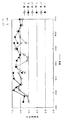
図10は、光源からの白色光束が均一照明手段201により均一化され、偏光変換手段202により偏光状態を変換される状態を説明するための図である。
FIG. 10 is a diagram for explaining a state in which the white light beam from the light source is made uniform by the
光源側からの白色光束は「1対の集光レンズアレイ(フライアイレンズアレイ)を対向配置して構成」した公知の均一照明手段201を透過して、偏光変換手段202に入射する。
The white light beam from the light source side is transmitted through a known
偏光変換手段202は、請求項11記載の光学素子に対する実施の1形態をなすものであり、光学基体202Aと、位相板部分202Bとを有している。
図10(a)に示すように、光学基体202Aの部分は、照明光の光軸に対して45度傾いた偏光分離面2021と反射面2022とを交互に有する。
The polarization conversion means 202 constitutes an embodiment of the optical element according to claim 11 and has an
As shown in FIG. 10A, the portion of the
偏光分離面2021は、入射光を偏光面が互いに直交する反射光S(以下「S成分」という。)と透過光P(以下「P成分」という。)とに分割する。反射面2022は、S成分を反射してP成分の進行方向と略同じ方向に向ける。
The
偏光分離面2021と反射面2022の組み合わせを1ユニットとし、このようなユニットの複数ユニットが、照明光の透過領域に渡って設けられて所謂「偏光プリズムレンズアレイ」をなし、アレイを構成する個々の偏光プリズムごとに、透過する照明光をS成分とP成分に分ける。
The combination of the
位相板部分202Bは、光学基体202Aから射出するS成分の偏光面を90度旋回させ、P成分の偏光方向に揃える。このようにして、偏光方向が揃った直線偏光の照明光が得られる。この照明光の偏光方向は勿論「各液晶表示素子の入射側偏光子の偏光方向」と同じである。
The
図10(b)は位相板部分202Bの部分を説明する図である。位相板部分202Bは、ガラス平板202B1の片面に形成された「屈折率:1.6以上の材料」による薄層202B2の表面に、断面矩形波状の微細凹凸構造2021B、2022B、2023B等がサブ波長構造として形成され、各微細凹凸構造2021B等は「2/1波長板相当の位相板」としての機能を付与されている。ガラス平板202B1は光学基体202Aにおける「方向の揃った照明光が射出する側の面」に一体化され、微細凹凸構造2021B等は「S成分が射出する部分」に形成されている。なお、位相板部分202Bと光学基体202Aとの接合は、薄層202B2を光学基体202Aの側としてもよく、このようにすると、微細凹凸構造をガラス平板202B1により良好に保護することができる。
FIG. 10B illustrates the
またガラス平板202B1を用いず、薄層202B2を光学基体202Aに直接形成してもよい。
Further, the thin layer 202B2 may be directly formed on the
図11は、請求項14記載の画像投射装置の実施の1形態を説明するための図である。繁雑を避けるため、混同の恐れがないと思われるものについては図8におけると同一の符号を付した。
FIG. 11 is a view for explaining one embodiment of the image projection apparatus according to
白色光源101から放射される白色光はリフレクタ102により反射され、ダイクロイックミラー103に入射すると、青色成分光が分離されてダイクロイックミラー103を透過し、緑色成分光と赤色成分光は反射されてダイクロイックミラー104に入射する。
When the white light emitted from the
緑色成分光はダイクロイックミラー104により反射され、赤色成分光はダイクロイックミラー104を透過する。このようにして、白色光が青、緑、赤の3原色に色分解される。青色成分光はミラー105により反射され、偏光ビームスプリッタ301に入射し、S偏光成分が反射され、1/4波長板相当の位相板307を介して反射型液晶表示素子304に入射する。
The green component light is reflected by the
緑色成分光は、偏光ビームスプリッタ302に入射し、S偏光成分が反射され、1/4波長板相当の位相板308を介して反射型液晶表示素子305に入射する。赤色成分光は偏光ビームスプリッタ303に入射し、S偏光成分が反射され、1/4波長板相当の位相板309を介して反射型液晶表示素子306に入射する。
The green component light enters the
各色成分光は対応する位相板を透過することにより円偏光となって、対応する反射型液晶表示素子に入射する。各反射型液晶表示素子304、305、306は、画像信号により反射光を変調し、変調された映像光を入射時と逆周りの円偏光とする。これらは、位相板307、308、309を透過することにより、往路の状態から偏光面が90度旋回し、対応する偏光ビームスプリッタ301、302、303に対してP偏光成分となり、偏光ビームスプリッタ301、302、303を透過してクロスプリズム113に入射し、図8の実施の形態と同様にして色合成されてクロスプリズム313から射出し、投射レンズ114によってスクリーン115にカラー映像として拡大投射される。このようにして、スクリーン115には画像が表示される。
Each color component light passes through the corresponding phase plate to become circularly polarized light and enters the corresponding reflective liquid crystal display element. Each of the reflective liquid
勿論、図11の実施の形態においても、図9の実施の形態と同様、白色光源101とダイクロイックミラー103との間に、均一照明手段201(オプチカルインテグレータ)と偏光変換素子202とを付加することにより、光利用効率を増大させることができる。
Of course, in the embodiment of FIG. 11 as well, the uniform illumination means 201 (optical integrator) and the
図8、図9に示した画像投射装置の実施の形態における位相板116、117、118の具体的な実施例を挙げる。
Specific examples of the
位相板116、117、118は何れも、厚さ:1.0mm、屈折率:1.45の平行平板状の石英ガラスを「ガラス平板」とし、その両面に「屈折率:1.6以上の材料」として「TiO2(屈折率:2.25)」を用い、厚さ:1μmの薄層をスパッタリングで形成し、これらの薄層の表面に断面矩形波状の微細凹凸構造をサブ波長構造として形成したものである。
Each of the
微細凹凸構造は、薄層の上に「電子ビームの走査により潜像の形成されるレジスト層」を形成し、このレジストに微細凹凸構造に対応するパターンを電子ビームにより描画して潜像を形成し、これを現像して「微細凹凸構造に対応するレジストパターン」を得、このレジストパターンをマスクとしてRIE(反応性イオンエッチング)で薄層を所望の溝深さにエッチングすることによって形成した。
各位相板の仕様と特性は以下のとおりである。
The fine concavo-convex structure forms a “resist layer on which a latent image is formed by scanning an electron beam” on a thin layer, and a pattern corresponding to the fine concavo-convex structure is drawn on the resist by an electron beam to form a latent image. This was developed to obtain a “resist pattern corresponding to the fine concavo-convex structure”, and the thin layer was etched to a desired groove depth by RIE (reactive ion etching) using this resist pattern as a mask.
The specifications and characteristics of each phase plate are as follows.
位相板116(青色映像光に対する1/2波長板相当の位相板)
薄層表面の微細凹凸構造
ピッチ:P=0.20μm
フィリングファクタ:f=0.6
ランドの幅:a=0.120μm
スペースの幅:b=0.080μm
溝深さ:H=0.380μm
光学特性
使用波長:420〜520nm
リタデーション:50±3%(50%は位相差:π)
0次透過率:0.88±7%(偏光成分:TE)
0.93±7%(偏光成分:TM) 。
Phase plate 116 (phase plate equivalent to a half-wave plate for blue image light)
Fine uneven structure on the surface of the thin layer Pitch: P = 0.20 μm
Filling factor: f = 0.6
Land width: a = 0.120 μm
Space width: b = 0.080 μm
Groove depth: H = 0.380 μm
optical properties
Wavelength used: 420-520 nm
Retardation: 50 ± 3% (50% is phase difference: π)
Zero-order transmittance: 0.88 ± 7% (polarization component: TE)
0.93 ± 7% (polarization component: TM).
位相板117(緑色映像光に対する1/2波長板相当の位相板)
薄層表面の微細凹凸構造
ピッチ:P=0.22μm
フィリングファクタ:f=0.7
ランドの幅:a=0.154μm
スペースの幅:b=0.066μm
溝深さ:H=0.543μm
光学特性
使用波長:520〜620nm
リタデーション:50±3%(50%は位相差:π)
0次透過率:0.88±9%(偏光成分:TE)
0.93±5%(偏光成分:TM) 。
Phase plate 117 (phase plate equivalent to a half-wave plate for green image light)
Fine uneven structure on the surface of the thin layer Pitch: P = 0.22 μm
Filling factor: f = 0.7
Land width: a = 0.154 μm
Space width: b = 0.066 μm
Groove depth: H = 0.543 μm
Optical properties Wavelength used: 520-620 nm
Retardation: 50 ± 3% (50% is phase difference: π)
Zero-order transmittance: 0.88 ± 9% (polarization component: TE)
0.93 ± 5% (polarization component: TM).
位相板118(赤色映像光に対する1/2波長板相当の位相板)
薄層表面の微細凹凸構造
ピッチ:P=0.30μm
フィリングファクタ:f=0.5
ランドの幅:a=0.150μm
スペースの幅:b=0.150μm
溝深さ:H=0.475μm
光学特性
使用波長:620〜700nm
リタデーション:50±4%(50%は位相差:π)
0次透過率:0.88±5%(偏光成分:TE)
0.93±4%(偏光成分:TM) 。
Phase plate 118 (a phase plate equivalent to a half-wave plate for red image light)
Fine uneven structure on the surface of the thin layer Pitch: P = 0.30 μm
Filling factor: f = 0.5
Land width: a = 0.150 μm
Space width: b = 0.150 μm
Groove depth: H = 0.475 μm
Optical properties Wavelength used: 620-700 nm
Retardation: 50 ± 4% (50% is phase difference: π)
Zero-order transmittance: 0.88 ± 5% (polarization component: TE)
0.93 ± 4% (polarization component: TM).
この実施例1における各位相板116、117、118の「リタデーション特性」を図12示す。3原色(青(B):420〜520nm、緑(G):520〜620nm、赤(R):620〜700nm)の各波長領域で、安定したリタデーションを確保できている。
FIG. 12 shows “retardation characteristics” of the
位相板116、117、118の「0次透過率」を図13に示す。上記3原色の範囲で80%以上の0次透過率を確保できている。図14は、上記各位相板におけるリタデーションの、入射角:0の場合と10度の場合の様子を示す。また、図15は上記各位相板について、0次透過率が入射角とともにどのように変化するかを示している。
位相板116、117、118のように、液晶表示素子の直後に配置されるような場合、入射角の変化は±10度程度を見積もればよく、その範囲においては各特性ともに安定した性能である。
“0th-order transmittance” of the
When the liquid crystal display element is disposed immediately after the liquid crystal display element, such as the
なお、実施例1では、位相板における薄層をガラス平板の両面に形成しているが、薄層をガラス平板の片面のみに形成し、この薄層に形成する微細凹凸形状の溝深さ:Hを、実施例1の場合の2倍(両面の薄層の、溝深さの和)としてもよい。 In Example 1, although the thin layer in the phase plate is formed on both surfaces of the glass flat plate, the thin layer is formed only on one surface of the glass flat plate, and the groove depth of the fine unevenness formed in this thin layer: H may be twice that of the first embodiment (the sum of the groove depths of the thin layers on both sides).
また、実施例1において形成された平板ガラス両面の薄層のうち、片面側の薄層を省略すれば、位相板は「1/4波長板相当」となり、図11の実施の形態における位相板307,308、309として用いることができる。 In addition, if the thin layer on one side of the thin layers on both sides of the flat glass formed in Example 1 is omitted, the phase plate is “equivalent to a quarter-wave plate”, and the phase plate in the embodiment of FIG. 307, 308, and 309 can be used.
なお、図8、図9の実施の形態では、3色いずれに対しても偏光軸の90度回転を必要とする場合を示しているが、3原色のいずれか1に対してのみ1/2波長板相当の位相板を必要とするような構成も可能である。 8 and 9 show a case in which the polarization axis needs to be rotated by 90 degrees for all three colors, but only 1/2 for any one of the three primary colors. A configuration requiring a phase plate equivalent to a wave plate is also possible.
11 ガラス平板
12a 薄層
12b 薄層
11 Glass
Claims (15)
微細凹凸構造におけるランドの幅がスペースの幅より広いことを特徴とする位相板。 The phase plate according to claim 1,
A phase plate characterized in that the land width in the fine relief structure is wider than the space width.
微細凹凸構造のピッチ:P、フィリングファクタ:fが、条件
(1) 0.1μm<P<0.4μm
(2) 0.5<f<0.8
を満足することを特徴とする位相板。 The phase plate according to claim 2,
Pitch of fine concavo-convex structure: P, filling factor: f, conditions (1) 0.1 μm <P <0.4 μm
(2) 0.5 <f <0.8
A phase plate satisfying the requirements.
微細凹凸構造の上に反射防止膜が形成されたことを特徴とする位相板。 In the phase plate according to any one of claims 1 to 3,
A phase plate, wherein an antireflection film is formed on a fine concavo-convex structure.
微細凹凸構造のランドの上のみに反射防止膜が形成されたことを特徴とする位相板。 In the phase plate according to any one of claims 1 to 3,
A phase plate, wherein an antireflection film is formed only on a land having a fine concavo-convex structure.
微細凹凸構造におけるランドの幅がスペースの幅より広いことを特徴とする光学素子。 The optical element according to claim 7.
An optical element characterized in that a land width in a fine relief structure is wider than a space width.
薄層における微細凹凸構造の上に反射防止膜が形成されたことを特徴とする光学素子。 The optical element according to claim 7 or 8,
An optical element, wherein an antireflection film is formed on a fine uneven structure in a thin layer.
薄層における微細凹凸構造のランドの上のみに反射防止膜が形成されたことを特徴とする光学素子。 The optical element according to claim 7 or 8,
An optical element, wherein an antireflection film is formed only on a land having a fine uneven structure in a thin layer.
光学基体が、入射光を偏光面が互いに直交する反射光と透過光に分割する偏光分離面と、上記反射光と透過光のうちの一方を反射して、他方の進行方向と略同じ方向に向ける反射面とを有し、
略同方向に揃った上記透過光および反射光が射出する面の側に、屈折率:1.6以上の材料による薄層が配置され、この薄層にサブ波長構造として形成されたランドとスペースによる断面矩形波状の微細凹凸構造が、上記反射光と透過光のうちの少なくとも一方の偏光面を変化させて双方の偏光面を一致させる位相板としての機能を有することを特徴とする光学素子。 The optical element according to any one of claims 6 to 10,
The optical substrate has a polarization separation surface that divides incident light into reflected light and transmitted light whose polarization planes are orthogonal to each other, reflects one of the reflected light and transmitted light, and is in substantially the same direction as the other traveling direction. A reflective surface to face,
A thin layer made of a material having a refractive index of 1.6 or more is disposed on the side of the surface from which the transmitted light and reflected light exit in substantially the same direction, and a land and a space formed as a subwavelength structure in the thin layer. An optical element characterized in that the fine concavo-convex structure having a rectangular wave shape in section has a function as a phase plate that changes the polarization plane of at least one of the reflected light and the transmitted light to make the polarization planes coincide with each other.
請求項1〜5の任意の1に記載の位相板、及び/または、請求項6〜11の任意の1に記載の光学素子が用いられたことを特徴とする画像投射装置。 In an image projection apparatus that guides a light beam from a light source to a liquid crystal display element and projects a display image of the liquid crystal display element on a display surface with a projection lens.
An image projection apparatus using the phase plate according to any one of claims 1 to 5 and / or the optical element according to any one of claims 6 to 11.
3原色に対応し各色の映像を個別に形成する3つの液晶表示素子と、
各液晶表示素子から射出した各色の映像光を合成するクロスプリズムを有し、
上記各液晶表示素子と上記クロスプリズムとの間の3光路の1以上に、1/2波長板相当の位相板として、請求項1〜5の任意の1に記載の位相板または請求項6〜10の任意の1に記載の光学素子を配置したことを特徴とする画像投射装置。 The image projection apparatus according to claim 12, wherein
Three liquid crystal display elements corresponding to the three primary colors and individually forming images of the respective colors;
It has a cross prism that synthesizes video light of each color emitted from each liquid crystal display element,
The phase plate according to any one of claims 1 to 5 or a phase plate according to any one of claims 1 to 5, as a phase plate corresponding to a half-wave plate in one or more of the three optical paths between the liquid crystal display elements and the cross prism. An image projection apparatus comprising: the optical element according to any one of 10;
3原色に対応し各色の映像を個別に形成する3つの反射型液晶表示素子と、
各反射型液晶表示素子から射出した各色の映像光を合成するクロスプリズムを有し、
上記各反射型液晶表示素子と上記クロスプリズムとの間の3光路の1以上に、1/4波長板相当の位相板として、請求項1〜5の任意の1に記載の位相板または請求項6〜10の任意の1に記載の光学素子を配置したことを特徴とする画像投射装置。 The image projection apparatus according to claim 13.
Three reflective liquid crystal display elements that individually form images of each color corresponding to the three primary colors;
Having a cross prism for synthesizing video light of each color emitted from each reflective liquid crystal display element;
The phase plate according to any one of claims 1 to 5 as a phase plate corresponding to a quarter-wave plate in one or more of the three optical paths between each of the reflective liquid crystal display elements and the cross prism. 6. An image projection apparatus comprising the optical element according to any one of 6 to 10.
光源からの光を直線偏光に揃える光学素子として、請求項11記載の光学素子を有することを特徴とする画像投射装置。 The image projection apparatus according to claim 13 or 14,
An image projection apparatus comprising the optical element according to claim 11 as an optical element for aligning light from a light source with linearly polarized light.
Priority Applications (1)
| Application Number | Priority Date | Filing Date | Title |
|---|---|---|---|
| JP2006212291A JP4814002B2 (en) | 2005-09-30 | 2006-08-03 | Phase plate manufacturing method, optical element and image projection apparatus |
Applications Claiming Priority (3)
| Application Number | Priority Date | Filing Date | Title |
|---|---|---|---|
| JP2005286872 | 2005-09-30 | ||
| JP2005286872 | 2005-09-30 | ||
| JP2006212291A JP4814002B2 (en) | 2005-09-30 | 2006-08-03 | Phase plate manufacturing method, optical element and image projection apparatus |
Publications (2)
| Publication Number | Publication Date |
|---|---|
| JP2007122017A true JP2007122017A (en) | 2007-05-17 |
| JP4814002B2 JP4814002B2 (en) | 2011-11-09 |
Family
ID=38145867
Family Applications (1)
| Application Number | Title | Priority Date | Filing Date |
|---|---|---|---|
| JP2006212291A Expired - Fee Related JP4814002B2 (en) | 2005-09-30 | 2006-08-03 | Phase plate manufacturing method, optical element and image projection apparatus |
Country Status (1)
| Country | Link |
|---|---|
| JP (1) | JP4814002B2 (en) |
Cited By (15)
| Publication number | Priority date | Publication date | Assignee | Title |
|---|---|---|---|---|
| JP2009048023A (en) * | 2007-08-21 | 2009-03-05 | Ricoh Opt Ind Co Ltd | Optical element |
| JP2009288406A (en) * | 2008-05-28 | 2009-12-10 | Canon Inc | Optical element and optical apparatus |
| JP2010072126A (en) * | 2008-09-17 | 2010-04-02 | Canon Inc | Optical element and optical apparatus |
| JP2010175805A (en) * | 2009-01-29 | 2010-08-12 | Canon Inc | Laminated thin film, phase plate and reflective liquid crystal display apparatus |
| JP2010211856A (en) * | 2009-03-09 | 2010-09-24 | Ricoh Opt Ind Co Ltd | Quarter-wave plate |
| JP2011232551A (en) * | 2010-04-28 | 2011-11-17 | Osaka Prefecture Univ | Optical component |
| WO2017061170A1 (en) * | 2015-10-05 | 2017-04-13 | Jxエネルギー株式会社 | Optical retarder member and projector |
| JP2018025748A (en) * | 2016-05-12 | 2018-02-15 | Jxtgエネルギー株式会社 | Optical retardation member and projector |
| JP2018072570A (en) * | 2016-10-28 | 2018-05-10 | リコーインダストリアルソリューションズ株式会社 | Speckle cancellation element and speckle cancellation mechanism |
| JP2018155795A (en) * | 2017-03-15 | 2018-10-04 | Jxtgエネルギー株式会社 | Optical retardation member, polarization conversion element, template, and manufacturing method of optical retardation member |
| CN108693585A (en) * | 2017-04-06 | 2018-10-23 | Jxtg能源株式会社 | The manufacturing method of optical phase difference component and optical phase difference component |
| JP2019032546A (en) * | 2014-06-02 | 2019-02-28 | Agc株式会社 | Image projection structure, manufacturing method of image projection structure, image projection method and window for automatic vehicle |
| JP2021504736A (en) * | 2017-11-21 | 2021-02-15 | アプライド マテリアルズ インコーポレイテッドApplied Materials,Incorporated | Manufacturing method of waveguide coupler |
| US11327218B2 (en) | 2017-11-29 | 2022-05-10 | Applied Materials, Inc. | Method of direct etching fabrication of waveguide combiners |
| KR20230094320A (en) * | 2021-12-21 | 2023-06-28 | 한국광기술원 | Image Output Apparatus with Improved Light Efficiency Including Geometrical Phase Prism and AR Apparatus Including the Same |
Citations (8)
| Publication number | Priority date | Publication date | Assignee | Title |
|---|---|---|---|---|
| JP2000221450A (en) * | 1999-01-29 | 2000-08-11 | Arisawa Mfg Co Ltd | Video device |
| JP2003207636A (en) * | 2002-01-15 | 2003-07-25 | Ricoh Co Ltd | Wavelength plate, optical pickup and optical disk device |
| JP2004077806A (en) * | 2002-08-19 | 2004-03-11 | Sanyo Electric Co Ltd | Phase plate optical element |
| JP2004093634A (en) * | 2002-08-29 | 2004-03-25 | Nippon Sheet Glass Co Ltd | Method of forming structure |
| JP2005107511A (en) * | 2003-09-08 | 2005-04-21 | Sony Corp | Picture projection device |
| JP2005128241A (en) * | 2003-10-23 | 2005-05-19 | Enplas Corp | Polarization conversion element |
| JP2005242083A (en) * | 2004-02-27 | 2005-09-08 | Canon Inc | Optical wavelength plate and manufacturing method therefor |
| JP2005259235A (en) * | 2004-03-11 | 2005-09-22 | Sanyo Electric Co Ltd | Optical pickup |
-
2006
- 2006-08-03 JP JP2006212291A patent/JP4814002B2/en not_active Expired - Fee Related
Patent Citations (8)
| Publication number | Priority date | Publication date | Assignee | Title |
|---|---|---|---|---|
| JP2000221450A (en) * | 1999-01-29 | 2000-08-11 | Arisawa Mfg Co Ltd | Video device |
| JP2003207636A (en) * | 2002-01-15 | 2003-07-25 | Ricoh Co Ltd | Wavelength plate, optical pickup and optical disk device |
| JP2004077806A (en) * | 2002-08-19 | 2004-03-11 | Sanyo Electric Co Ltd | Phase plate optical element |
| JP2004093634A (en) * | 2002-08-29 | 2004-03-25 | Nippon Sheet Glass Co Ltd | Method of forming structure |
| JP2005107511A (en) * | 2003-09-08 | 2005-04-21 | Sony Corp | Picture projection device |
| JP2005128241A (en) * | 2003-10-23 | 2005-05-19 | Enplas Corp | Polarization conversion element |
| JP2005242083A (en) * | 2004-02-27 | 2005-09-08 | Canon Inc | Optical wavelength plate and manufacturing method therefor |
| JP2005259235A (en) * | 2004-03-11 | 2005-09-22 | Sanyo Electric Co Ltd | Optical pickup |
Cited By (24)
| Publication number | Priority date | Publication date | Assignee | Title |
|---|---|---|---|---|
| JP2009048023A (en) * | 2007-08-21 | 2009-03-05 | Ricoh Opt Ind Co Ltd | Optical element |
| US8339708B2 (en) | 2008-05-28 | 2012-12-25 | Canon Kabuskiki Kaisha | Optical element and optical apparatus |
| JP2009288406A (en) * | 2008-05-28 | 2009-12-10 | Canon Inc | Optical element and optical apparatus |
| JP2010072126A (en) * | 2008-09-17 | 2010-04-02 | Canon Inc | Optical element and optical apparatus |
| JP2010175805A (en) * | 2009-01-29 | 2010-08-12 | Canon Inc | Laminated thin film, phase plate and reflective liquid crystal display apparatus |
| JP2010211856A (en) * | 2009-03-09 | 2010-09-24 | Ricoh Opt Ind Co Ltd | Quarter-wave plate |
| JP2011232551A (en) * | 2010-04-28 | 2011-11-17 | Osaka Prefecture Univ | Optical component |
| JP2019032546A (en) * | 2014-06-02 | 2019-02-28 | Agc株式会社 | Image projection structure, manufacturing method of image projection structure, image projection method and window for automatic vehicle |
| WO2017061170A1 (en) * | 2015-10-05 | 2017-04-13 | Jxエネルギー株式会社 | Optical retarder member and projector |
| CN108139525A (en) * | 2015-10-05 | 2018-06-08 | Jxtg能源株式会社 | optical phase difference component and projector |
| JP2018025748A (en) * | 2016-05-12 | 2018-02-15 | Jxtgエネルギー株式会社 | Optical retardation member and projector |
| TWI733793B (en) * | 2016-05-12 | 2021-07-21 | 日商Jxtg能源股份有限公司 | Optical phase difference component and projector |
| JP2018072570A (en) * | 2016-10-28 | 2018-05-10 | リコーインダストリアルソリューションズ株式会社 | Speckle cancellation element and speckle cancellation mechanism |
| CN108627900A (en) * | 2017-03-15 | 2018-10-09 | Jxtg能源株式会社 | The manufacturing method of optical phase difference component, polarization conversion element, template and optical phase difference component |
| JP2018155795A (en) * | 2017-03-15 | 2018-10-04 | Jxtgエネルギー株式会社 | Optical retardation member, polarization conversion element, template, and manufacturing method of optical retardation member |
| TWI743316B (en) * | 2017-03-15 | 2021-10-21 | 日商Jxtg能源股份有限公司 | Optical retardation member, polarization conversion element, template, and manufacturing method of optical retardation member |
| JP2018180112A (en) * | 2017-04-06 | 2018-11-15 | Jxtgエネルギー株式会社 | Optical phase difference member and production method of optical phase difference member |
| CN108693585A (en) * | 2017-04-06 | 2018-10-23 | Jxtg能源株式会社 | The manufacturing method of optical phase difference component and optical phase difference component |
| JP7064290B2 (en) | 2017-04-06 | 2022-05-10 | Eneos株式会社 | Optical retardation member and manufacturing method of optical retardation member |
| JP2021504736A (en) * | 2017-11-21 | 2021-02-15 | アプライド マテリアルズ インコーポレイテッドApplied Materials,Incorporated | Manufacturing method of waveguide coupler |
| US11327218B2 (en) | 2017-11-29 | 2022-05-10 | Applied Materials, Inc. | Method of direct etching fabrication of waveguide combiners |
| US11662516B2 (en) | 2017-11-29 | 2023-05-30 | Applied Materials, Inc. | Method of direct etching fabrication of waveguide combiners |
| KR20230094320A (en) * | 2021-12-21 | 2023-06-28 | 한국광기술원 | Image Output Apparatus with Improved Light Efficiency Including Geometrical Phase Prism and AR Apparatus Including the Same |
| KR102575167B1 (en) | 2021-12-21 | 2023-09-06 | 한국광기술원 | Image Output Apparatus with Improved Light Efficiency Including Geometrical Phase Prism and AR Apparatus Including the Same |
Also Published As
| Publication number | Publication date |
|---|---|
| JP4814002B2 (en) | 2011-11-09 |
Similar Documents
| Publication | Publication Date | Title |
|---|---|---|
| JP4814002B2 (en) | Phase plate manufacturing method, optical element and image projection apparatus | |
| JP4842763B2 (en) | Optical element and optical device | |
| US6947215B2 (en) | Optical element, optical functional device, polarization conversion device, image display apparatus, and image display system | |
| JP4847304B2 (en) | Optical element and optical device | |
| US8009355B2 (en) | Optical element having periodic structure and optical apparatus using the same | |
| JP4593894B2 (en) | Optical encoder | |
| US7236655B2 (en) | Polarization element and optical device using polarization element | |
| JP2008008990A (en) | Wavelength plate, image projector, and optical pick-up | |
| EP1826593B1 (en) | Optical element and image projecting apparatus | |
| JP4510547B2 (en) | Polarization separating element and projection apparatus having the same | |
| JP4125114B2 (en) | Optical element, optical modulation element, and image display device | |
| JP4427026B2 (en) | Polarizer and polarization separation element | |
| JP2007033676A (en) | Polarized light converting optical element, optical modulation module, and projection type image display apparatus | |
| JP2012226208A (en) | Polarization separation element, and polarization conversion element and image projection device using the same | |
| JP2008185768A (en) | Wavelength plate and optical device | |
| JP4537115B2 (en) | Polarization separation prism | |
| JP2011186252A (en) | Polarization converting element | |
| JP2009032698A (en) | Illumination optical system | |
| JP2008224786A (en) | Optical switching element, switching element, optical switching element array, and image display device | |
| JP5188524B2 (en) | Polarization separation element | |
| JP2008070691A (en) | Wavelength plate, lighting apparatus and projector | |
| JP5605144B2 (en) | Color composition unit and projection display device | |
| JP2010072126A (en) | Optical element and optical apparatus | |
| JP2006078917A (en) | Polarizing element, liquid crystal display panel and liquid crystal display | |
| JP2007003756A (en) | Polarizing optical element, optical part assembly and optical apparatus |
Legal Events
| Date | Code | Title | Description |
|---|---|---|---|
| A621 | Written request for application examination |
Free format text: JAPANESE INTERMEDIATE CODE: A621 Effective date: 20090409 |
|
| A977 | Report on retrieval |
Free format text: JAPANESE INTERMEDIATE CODE: A971007 Effective date: 20100916 |
|
| A131 | Notification of reasons for refusal |
Free format text: JAPANESE INTERMEDIATE CODE: A131 Effective date: 20101005 |
|
| A521 | Written amendment |
Free format text: JAPANESE INTERMEDIATE CODE: A523 Effective date: 20101206 |
|
| A131 | Notification of reasons for refusal |
Free format text: JAPANESE INTERMEDIATE CODE: A131 Effective date: 20110125 |
|
| A521 | Written amendment |
Free format text: JAPANESE INTERMEDIATE CODE: A523 Effective date: 20110328 |
|
| A02 | Decision of refusal |
Free format text: JAPANESE INTERMEDIATE CODE: A02 Effective date: 20110426 |
|
| A521 | Written amendment |
Free format text: JAPANESE INTERMEDIATE CODE: A523 Effective date: 20110725 |
|
| A911 | Transfer of reconsideration by examiner before appeal (zenchi) |
Free format text: JAPANESE INTERMEDIATE CODE: A911 Effective date: 20110729 |
|
| TRDD | Decision of grant or rejection written | ||
| A01 | Written decision to grant a patent or to grant a registration (utility model) |
Free format text: JAPANESE INTERMEDIATE CODE: A01 Effective date: 20110823 |
|
| A01 | Written decision to grant a patent or to grant a registration (utility model) |
Free format text: JAPANESE INTERMEDIATE CODE: A01 |
|
| A61 | First payment of annual fees (during grant procedure) |
Free format text: JAPANESE INTERMEDIATE CODE: A61 Effective date: 20110825 |
|
| R150 | Certificate of patent or registration of utility model |
Ref document number: 4814002 Country of ref document: JP Free format text: JAPANESE INTERMEDIATE CODE: R150 Free format text: JAPANESE INTERMEDIATE CODE: R150 |
|
| FPAY | Renewal fee payment (event date is renewal date of database) |
Free format text: PAYMENT UNTIL: 20140902 Year of fee payment: 3 |
|
| R250 | Receipt of annual fees |
Free format text: JAPANESE INTERMEDIATE CODE: R250 |
|
| R250 | Receipt of annual fees |
Free format text: JAPANESE INTERMEDIATE CODE: R250 |
|
| R250 | Receipt of annual fees |
Free format text: JAPANESE INTERMEDIATE CODE: R250 |
|
| R250 | Receipt of annual fees |
Free format text: JAPANESE INTERMEDIATE CODE: R250 |
|
| R250 | Receipt of annual fees |
Free format text: JAPANESE INTERMEDIATE CODE: R250 |
|
| LAPS | Cancellation because of no payment of annual fees |