JP2007109199A - Buffer device, control method for buffer device, and information processor - Google Patents
Buffer device, control method for buffer device, and information processor Download PDFInfo
- Publication number
- JP2007109199A JP2007109199A JP2006045374A JP2006045374A JP2007109199A JP 2007109199 A JP2007109199 A JP 2007109199A JP 2006045374 A JP2006045374 A JP 2006045374A JP 2006045374 A JP2006045374 A JP 2006045374A JP 2007109199 A JP2007109199 A JP 2007109199A
- Authority
- JP
- Japan
- Prior art keywords
- circuit
- buffer
- clock
- peripheral
- access
- Prior art date
- Legal status (The legal status is an assumption and is not a legal conclusion. Google has not performed a legal analysis and makes no representation as to the accuracy of the status listed.)
- Withdrawn
Links
Images


Abstract
Description
本発明は、バッファ装置、バッファ装置の制御方法及び情報処理装置に関する。 The present invention relates to a buffer device, a control method for the buffer device, and an information processing device.
異なるクロックで動作する回路間のデータ転送に関しては、例えば2ポートメモリを間に置き、各ポートをそれぞれの異なるクロックに同期してアクセスする方法や、異なるクロック間で動作する回路の間に2段バッファを置き、このバッファをデータ及び必要な制御信号をデータを受ける側のクロックで制御する方法の2方法が一般的である。
しかし上記の2方法では基本的にクロックの種類が3以上の場合の対応ができないという問題点があった。 However, the above two methods have a problem in that it is basically impossible to cope with the case where the clock type is 3 or more.
クロックの種類が3以上の場合は、上記2方法の回路をそれぞれが持つ必要があり、ホストインターフェイス(バスインターフェイス)の設計変更が必要であり、結果的に全ての周辺回路でバッファを持つことになる。 If the clock type is 3 or more, each of the above two methods must have a circuit, and the host interface (bus interface) must be redesigned. As a result, all peripheral circuits have buffers. Become.
このバッファリングにより、ホストCPUから各周辺装置へのアクセス順番と実際の周辺回路へのアクセス順番に時間差が生じ、制御が難しくなるという問題も出る。 Due to this buffering, a time difference occurs between the access order from the host CPU to each peripheral device and the access order to the actual peripheral circuit, which causes a problem that control becomes difficult.
本発明は以上のような問題点に鑑みてなされたものであり、その目的とするところは、様々な動作クロックで動作する既存の周辺回路を容易に接続することのできるバッファ回路を提供することで、システム・オン・チップを容易にすることを目的とする。 The present invention has been made in view of the above problems, and an object of the present invention is to provide a buffer circuit capable of easily connecting existing peripheral circuits operating with various operation clocks. The purpose is to facilitate system-on-chip.
(1)本発明は、
周波数の異なるクロックで動作する第1の回路と第2の回路の間に存在するバッファ装置であって、
第1の回路と第2の回路のデータのやり取りに必要なアドレス及びデータの少なくとも一方を格納するバッファと、
第1の回路とバッファの接続部である第1のインターフェース部と、
第2の回路とバッファの接続部である第2のインターフェース部と、
第1の回路及び第2の回路のバッファへのアクセス状況に基づき、前記バッファに供給するクロックを切り替えるタイミングを判断し、バッファに供給するクロックの選択または切り替えを指示するためのクロック切り替え制御信号を生成するクロック切り替え制御回路と、
第1の回路の動作クロック及び第2の回路の動作クロックを含む複数のクロックを入力し、前記クロック切り替え信号に基づきいずれかのクロックを選択して前記バッファに供給するクロック切り替え回路と、
を含むことを特徴とする。
(1) The present invention
A buffer device that exists between a first circuit and a second circuit that operate with clocks having different frequencies,
A buffer for storing at least one of an address and data necessary for data exchange between the first circuit and the second circuit;
A first interface unit which is a connection unit between the first circuit and the buffer;
A second interface unit that is a connection between the second circuit and the buffer;
Based on the access status to the buffers of the first circuit and the second circuit, the timing for switching the clock supplied to the buffer is determined, and a clock switching control signal for instructing selection or switching of the clock supplied to the buffer is provided. A clock switching control circuit to be generated;
A clock switching circuit that receives a plurality of clocks including an operation clock of the first circuit and an operation clock of the second circuit, selects one of the clocks based on the clock switching signal, and supplies the selected clock to the buffer;
It is characterized by including.
第1のインターフェース部は、第1の回路が前記バッファにアクセスする際の信号のやり取りをするためのインターフェース部である。 The first interface unit is an interface unit for exchanging signals when the first circuit accesses the buffer.
第2のインターフェース部は、第2の回路が前記バッファにアクセスする際の信号のやり取りをするためのインターフェース部である。 The second interface unit is an interface unit for exchanging signals when the second circuit accesses the buffer.
クロック切り替え制御回路は、第1の回路がバッファに対して読み書きを行う場合には、バッファに第1の回路の動作周波数のクロックを供給し、第2の回路がバッファに対して読み書きを行う場合にはバッファに第2の回路の動作周波数のクロックを供給するように、バッファに供給するクロックを切り替えるためのクロック切り替え制御信号を生成する。 When the first circuit reads / writes to / from the buffer, the clock switching control circuit supplies the buffer with the clock having the operating frequency of the first circuit, and the second circuit reads / writes from / to the buffer. In this case, a clock switching control signal for switching the clock supplied to the buffer is generated so that the clock having the operating frequency of the second circuit is supplied to the buffer.
そしてクロック切り替え回路は、第1の回路の動作周波数のクロックと第2の回路の動作周波数のクロックを含む複数のクロックを入力し、所定の制御信号に基づきいづれかのクロックを選択して、バッファに出力する選択回路によって実現することができる。 The clock switching circuit receives a plurality of clocks including a clock having an operating frequency of the first circuit and a clock having an operating frequency of the second circuit, selects one of the clocks based on a predetermined control signal, and inputs the clock to the buffer. This can be realized by an output selection circuit.
ここにおいて第2の回路として複数の異なる周波数の回路が接続されるようにしてもよい。このような場合には、クロック切り替え回路は、これら複数の異なる周波数の回路の動作周波数を入力して、第1の回路の動作周波数と複数の異なる周波数の回路の動作周波数の中からクロック切り替え制御信号に基づきいずれかの周波数を選択して出力することになる。 Here, a plurality of circuits having different frequencies may be connected as the second circuit. In such a case, the clock switching circuit inputs the operating frequencies of the plurality of circuits having different frequencies, and performs clock switching control from among the operating frequencies of the first circuit and the plurality of different frequencies. One of the frequencies is selected and output based on the signal.
(2)本発明のバッファ装置は、
前記バッファは、
複数段で構成されており、
前記クロック切り替え制御回路は、
第1の回路及び第2の回路の各段のバッファへのアクセス状況に基づき、前記各段のバッファに供給するクロックを切り替えるタイミングを判断し、各段に対応したクロック切り替え制御信号を生成し、
前記クロック切り替え回路は、
前記バッファの格段に対応して第1の回路の動作クロック及び第2の回路の動作クロックを含む複数のクロックを入力し、前記各段に対応したクロック切り替え信号に基づきいずれかのクロックを選択して各段のバッファに供給することを特徴とする。
(2) The buffer device of the present invention includes:
The buffer is
It consists of multiple stages,
The clock switching control circuit includes:
Based on the access status to the buffer of each stage of the first circuit and the second circuit, the timing to switch the clock supplied to the buffer of each stage is determined, and a clock switching control signal corresponding to each stage is generated,
The clock switching circuit is
A plurality of clocks including an operation clock of the first circuit and an operation clock of the second circuit are input corresponding to the exceptional level of the buffer, and one of the clocks is selected based on the clock switching signal corresponding to each stage. Supply to the buffer of each stage.
(3)本発明のバッファ装置は、
前記第2のインターフェース部は、
第1の回路のバッファへの書き込みが発生すると書き込みのあった段のバッファへのポインターを格納するためのFIFOを含み、
前記FIFOの出力順に先入先出で第2の回路からバッファへのアクセスを許可するように制御することを特徴とする。
(3) The buffer device of the present invention includes:
The second interface unit includes:
A FIFO for storing a pointer to the buffer at the stage of writing when writing to the buffer of the first circuit occurs;
Control is performed so as to permit access to the buffer from the second circuit in first-in first-out order in the output order of the FIFO.
(4)本発明のバッファ装置は、
前記バッファ装置は、
周波数の異なるクロックで動作する複数の周辺回路と前記複数の周辺回路を制御する制御部の間に存在するバッファ装置であって、
前記第1のインターフェース部は、
前記制御部を接続するホストポート又はバスとして構成され、
前記第2のインターフェース部は
前記複数の周辺回路に対応する複数の周辺回路インターフェース回路含み、
前記バッファは、
制御部と周辺装置間のアクセスに必要なアドレス及びデータの少なくとも一方を格納することを特徴とする。
(4) The buffer device of the present invention includes:
The buffer device includes:
A buffer device that exists between a plurality of peripheral circuits that operate with clocks having different frequencies and a control unit that controls the plurality of peripheral circuits,
The first interface unit includes:
It is configured as a host port or bus that connects the control unit,
The second interface unit includes a plurality of peripheral circuit interface circuits corresponding to the plurality of peripheral circuits,
The buffer is
It stores at least one of an address and data necessary for access between the control unit and the peripheral device.
(5)本発明のバッファ装置は、
前記各周辺回路インターフェース回路は、
各周辺回路毎に、第1の回路のバッファへの当該周辺回路に対する書き込みが発生すると書き込みのあった段のバッファへのポインターを格納するためのFIFOを含み、前記FIFOの出力順に先入先出で当該周辺回路からバッファへのアクセスを許可するように制御することを特徴とする。
(5) The buffer device of the present invention includes:
Each of the peripheral circuit interface circuits is
Each peripheral circuit includes a FIFO for storing a pointer to the buffer at the stage where writing has been performed when writing to the buffer of the first circuit occurs in the buffer of the first circuit. Control is performed to permit access to the buffer from the peripheral circuit.
(6)本発明のバッファ装置は、
前記各周辺回路は他の周辺回路とは独立したバスを有しており、
前記各周辺回路インターフェース回路は、
対応する周辺回路のバスに接続されていることを特徴とする。
(6) The buffer device of the present invention includes:
Each peripheral circuit has a bus independent of other peripheral circuits,
Each of the peripheral circuit interface circuits is
It is connected to a bus of a corresponding peripheral circuit.
このようにすること並列モードでの動作が可能となる。 This makes it possible to operate in a parallel mode.
(7)本発明のバッファ装置は、
前記クロック切り替え制御回路は、
第1の回路のバッファへの書き込みの終了を検出したら、当該バッファへ供給するクロックを、第2の回路の動作クロックに切り替えるように指示するクロック切り替え制御信号を生成することを特徴とする。
(7) The buffer device of the present invention includes:
The clock switching control circuit includes:
When the end of writing to the buffer of the first circuit is detected, a clock switching control signal for instructing to switch the clock supplied to the buffer to the operation clock of the second circuit is generated.
(8)本発明のバッファ装置は、
前記バッファは、
バッファに書き込まれた内容が第2の回路に対する読み出し又は書き込みのいずれであるかを識別するためのR/W識別フラグを含み、
前記クロック切り替え制御回路は、
R/W識別フラグが書き込みを示している場合には、バッファの内容が第2の回路から読み出されたことを検出したら、当該バッファへ供給するクロックを第1の回路の動作クロックに切り替えるように指示するクロック切り替え制御信号を生成することを特徴とする。
(8) The buffer device of the present invention includes:
The buffer is
An R / W identification flag for identifying whether the content written in the buffer is a read or write to the second circuit;
The clock switching control circuit includes:
When the R / W identification flag indicates writing, when it is detected that the buffer contents have been read from the second circuit, the clock supplied to the buffer is switched to the operation clock of the first circuit. Generating a clock switching control signal for instructing;
(9)本発明のバッファ装置は、
前記バッファは、
バッファに書き込まれた内容が第2の回路に対する読み出し又は書き込みのいずれであるかを識別するためのR/W識別フラグを含み、
前記クロック切り替え制御回路は、
R/W識別フラグが読み出しを示している場合には、第2の回路からバッファへの書き込みが行われたことを検出したら、当該バッファへ供給するクロックを、第1の回路の動作クロックに切り替えるように指示するクロック切り替え制御信号を生成することを特徴とする。
(9) The buffer device of the present invention includes:
The buffer is
An R / W identification flag for identifying whether the content written in the buffer is a read or write to the second circuit;
The clock switching control circuit includes:
When the R / W identification flag indicates reading, when it is detected that writing from the second circuit to the buffer has been performed, the clock supplied to the buffer is switched to the operation clock of the first circuit. Generating a clock switching control signal for instructing to do so.
(10)本発明のバッファ装置は、
前記バッファは、
バッファに書き込まれた内容が第2の回路に対する読み出し又は書き込みのいずれであるかを識別するためのR/W識別フラグを含み、
前記クロック切り替え制御回路は、
R/W識別フラグが読み出しを示している場合には、第2の回路から読み出し終了を検出し、読み出したデータを第1の回路へ出力したら、当該バッファへ供給するクロックを、第1の回路の動作クロックに切り替えるように指示するクロック切り替え制御信号を生成することを特徴とする。
(10) The buffer device of the present invention includes:
The buffer is
An R / W identification flag for identifying whether the content written in the buffer is a read or write to the second circuit;
The clock switching control circuit includes:
When the R / W identification flag indicates reading, when the end of reading is detected from the second circuit and the read data is output to the first circuit, the clock supplied to the buffer is supplied to the first circuit. A clock switching control signal for instructing switching to the operation clock is generated.
(11)本発明のバッファ装置は、
逐次モードであるか並列モードであるかの情報が記憶されるモード設定レジスタと、
モード設定レジスタの値が逐次モードであることを示している場合には第1の回路からのアクセスの順番に処理を実行するように制御し、モード設定レジスタの値が並列モードであることを示している場合には第1の回路からのアクセスの順番によらず処理を実行するように制御する回路と、を含み、
前記モード設定レジスタの値は第1の回路からの指示信号に基づき設定されることを特徴とする。
(11) The buffer device of the present invention includes:
A mode setting register for storing information on whether the mode is the sequential mode or the parallel mode;
When the value of the mode setting register indicates the sequential mode, control is performed so that the processing is executed in the order of access from the first circuit, and the value of the mode setting register indicates the parallel mode. And a circuit that controls to execute the process regardless of the order of access from the first circuit,
The value of the mode setting register is set based on an instruction signal from the first circuit.
(12)本発明は、上記のいずれかに記載のバッファ装置及び第1の回路及び第2の回路を含むことを特徴とする情報処理装置である。 (12) The present invention is an information processing apparatus including the buffer device according to any one of the above, a first circuit, and a second circuit.
請求項1乃至11のいずれかに記載のバッファ装置及び第1の回路及び第2の回路を含むことを特徴とする情報処理装置。 An information processing apparatus comprising the buffer device according to claim 1, a first circuit, and a second circuit.
(13)本発明は、
周波数の異なるクロックで動作する第1の回路と第2の回路の間に存在し、第1の回路と第2の回路のデータのやり取りに必要なアドレス及びデータの少なくとも一方を格納するバッファを含むバッファ装置の制御方法であって、
第1の回路及び第2の回路のバッファへのアクセス状況に基づき、前記バッファに供給するクロックを切り替えるタイミングを判断し、バッファに供給するクロックの選択または切り替えを指示するためのクロック切り替え制御信号を生成するステップと、
第1の回路の動作クロック及び第2の回路の動作クロックを含む複数のクロックを入力し、前記クロック切り替え信号に基づきいずれかのクロックを選択して前記バッファに供給するステップとを、
を含むことを特徴とする。
(13) The present invention provides:
A buffer that exists between a first circuit and a second circuit that operate with clocks having different frequencies and stores at least one of an address and data necessary for data exchange between the first circuit and the second circuit; A control method for a buffer device, comprising:
Based on the access status to the buffers of the first circuit and the second circuit, the timing for switching the clock supplied to the buffer is determined, and a clock switching control signal for instructing selection or switching of the clock supplied to the buffer is provided. Generating step;
Inputting a plurality of clocks including an operation clock of the first circuit and an operation clock of the second circuit, selecting any one of the clocks based on the clock switching signal, and supplying the selected clock to the buffer;
It is characterized by including.
(14)本発明の制御方法は、
前記第1の回路からの指示信号に基づき実行モードを設定するステップと、
実行モードが逐次モードに設定されている場合には第1の回路からのアクセスの順番に処理を実行するように制御し、並列モードに設定されている場合には第1の回路からのアクセスの順番によらず処理を実行するように制御するステップと、
を含むことを特徴とする。
(14) The control method of the present invention includes:
Setting an execution mode based on an instruction signal from the first circuit;
When the execution mode is set to the sequential mode, control is performed so that processing is executed in the order of access from the first circuit. When the execution mode is set to the parallel mode, access from the first circuit is controlled. A step for controlling the processing to be executed regardless of the order; and
It is characterized by including.
1.集積回路装置
以下、本発明の好適な実施形態について図面を用いて詳細に説明する。
1. Integrated Circuit Device Hereinafter, preferred embodiments of the present invention will be described in detail with reference to the drawings.
図1は、本実施の形態のバッファ装置について説明するための図である。 FIG. 1 is a diagram for explaining a buffer device according to the present embodiment.
本実施の形態のバッファ装置100は、周波数の異なる動作クロックで動作する第1の回路180と第2の回路190の間に存在するバッファ装置100であって、第1のインターフェース部130、第2のインターフェース部140、バッファ110、制御部170、クロック切り替え部120を含む。
The
また本実施の形態の情報処理装置300は、バッファ装置100、第1の回路180、第2の回路190とを含む。
The information processing apparatus 300 according to the present embodiment includes a
第1のインターフェース部130は、第1の回路を接続するためのインターフェース回路である。第2のインターフェース部140は第2の回路を接続するためのインターフェース回路である。
The
第1のインターフェース部130は、第1の回路(制御部)180を接続するホストポート又はバスへの接続部(図示せず)を含む。
The
第2のインターフェース部140は、第2の回路(周辺回路)190を接続するペリフェラルポート(図示せず)とFIFO142とセレクタ146とバスドライバレシーバ148を含む。
The
ペリフェラルポート(図示せず)には、該ペリフェラルポートに接続する第2の回路(周辺回路)190のクロック入力端子を持つようにしてもよい。 A peripheral port (not shown) may have a clock input terminal of the second circuit (peripheral circuit) 190 connected to the peripheral port.
FIFO142は、前記アドレスバッファ及びデータバッファのポインターを格納するもので、第1の回路180のバッファ110への書き込みが発生すると書き込みのあった段のバッファへのポインターを格納する。FIFO142の出力順に先入先出で第2の回路190からバッファへのアクセスを許可するように制御する。
The
バッファ110は第1の回路180と第2の回路190のデータのやり取りに必要なアドレス及びデータの少なくとも一方を格納するバッファである。
The
前記バッファ110を、複数段(110−0,110−1、・・・110−n)で構成して、前記クロック切り替え部120(120−0、120−1,・・・、120−n)は、前記バッファの各段110−0、110−1、・・・110−nに対応して設け、前記バッファの各段毎に供給するクロックを切り替える。
The
またバッファをメモリ空間あるいはIO空間にマッピングされたアドレスを格納する複数のアドレスバッファと、該アドレスバッファに対応した書込みデータ及び読み出しデータを格納するデータバッファとで構成するようにしてもよい。 Further, the buffer may be composed of a plurality of address buffers for storing addresses mapped in the memory space or IO space, and a data buffer for storing write data and read data corresponding to the address buffers.
また前記バッファ110−0、110−1、110−2、・・・に書き込まれた順番に前記各周辺回路にアクセスするようにしてもよい(逐次モード)。 The peripheral circuits may be accessed in the order written in the buffers 110-0, 110-1, 110-2,... (Sequential mode).
制御部170は、第1の回路(ホスト)からのアクセス全般の応答制御とバッファ制御を行う。制御部170は、クロック切り替え制御回路150を含む。
The
クロック切り替え制御回路150は、第1の回路180及び第2の回路190のバッファ110へのアクセス状況に基づき、前記バッファ110に供給するクロックを切り替えるタイミングを判断し、バッファに供給するクロックの選択または切り替えを指示するためのクロック切り替え制御信号152を生成する。
The clock
クロック切り替え制御回路150は、バッファが複数段で構成されている場合には、第1の回路180及び第2の回路190の各段のバッファ110−0、110−1、・・・、110−nへのアクセス状況に基づき、前記各段のバッファ110−0、110−1、・・・、110−nに供給するクロックを切り替えるタイミングを判断し、各段に対応したクロック切り替え制御信号152−0、152−1、・・・、152−nを生成する。
The clock
前記クロック切り替え制御回路150は、第1の回路のバッファへの書き込みの終了を検出したら、当該バッファへ供給するクロックを、第2の回路の動作クロックに切り替えるように指示するクロック切り替え制御信号を生成するようにしてもよい。
When the clock switching
ここで前記バッファ110は、バッファに書き込まれた内容が第2の回路190に対する読み出し又は書き込みのいずれであるかを識別するためのR/W識別フラグを含むようにしてもよい。
Here, the
かかる場合には、クロック切り替え制御回路150は、R/W識別フラグが書き込みを示している場合には、バッファ110の内容が第2の回路190から読み出されたことを検出したら、当該バッファ110へ供給するクロックを第1の回路の動作クロックに切り替えるように指示するクロック切り替え制御信号152を生成するようにしてもよい。
また前記クロック切り替え制御回路150は、R/W識別フラグが読み出しを示している場合には、第2の回路190からバッファへの書き込みが行われたことを検出したら、当該バッファ110へ供給するクロックを、第1の回路180の動作クロックに切り替えるように指示するクロック切り替え制御信号152を生成するようにしてもよい。第2の回路からの読み出しデータがバッファに格納されるパスは図示していないが、バッファの入力側にセレクタを設け、バッファの出力を第1の回路に与えるパスを用意することで可能である。
第2の回路からの読み出しデータは、第1の回路の動作クロックの変化に対して安定してデータを出力することができるため、読み出しデータはバッファリングせずに、直接第2の回路から第1の回路に出力するようにしてもよい。この場合、バッファの動作クロックの切り替えは、第2の回路からデータの読み出し終了を検出した後で行うようにしてもよい。
In such a case, when the R / W identification flag indicates writing, the clock switching
In addition, when the R / W identification flag indicates reading, the clock switching
Since the read data from the second circuit can be output stably with respect to the change in the operation clock of the first circuit, the read data is directly buffered from the second circuit without being buffered. 1 may be output to one circuit. In this case, the operation clock of the buffer may be switched after detecting the end of reading data from the second circuit.
クロック切り替え部120は、第1の回路180の動作クロック及び第2の回路190の動作クロックを含む複数のクロックを入力し、前記クロック切り替え信号152に基づきいずれかのクロックを選択して前記バッファ110に供給する。
The
第1の回路180の動作クロック182は、例えば第1のインターフェース部130を介して、第1の回路から入力するようにしてもよい。
The
また第2の回路の動作クロックは、例えば第2のインターフェース部140を介して、第2の回路から入力するようにしてもよい。
The operation clock of the second circuit may be input from the second circuit via the
またアドレスバッファに有効な値がない場合は該アドレスバッファ及び対応するデータバッファは第1の回路(制御部)180が接続されるホストポート又はバスの動作クロックで動作するようにしてもよい。 When there is no valid value in the address buffer, the address buffer and the corresponding data buffer may be operated with the operation clock of the host port or bus to which the first circuit (control unit) 180 is connected.
そして第1の回路(制御部)180からホストポートに接続した周辺回路にアクセスすると、アドレスとデータが有効な値のない前記アドレスバッファ及びデータバッファに一旦書き込まれるようにしてもよい。 Then, when the peripheral circuit connected to the host port is accessed from the first circuit (control unit) 180, the address and data may be temporarily written in the address buffer and data buffer having no valid values.
そして動作クロックが該ペリフェラルポートから入力されるクロックに切り替わり、該バッファのポインターが該ペリフェラルポートに対応したFIFO142に書き込まれ、該FIFO142に格納されたポインターにより前記アドレスバッファ、データバッファの内容が読み出され、該ペリフェラルポートに接続された第2の回路(周辺回路)190に対してのアクセスが行われるようにしてもよい。
Then, the operation clock is switched to the clock input from the peripheral port, the pointer of the buffer is written to the
アクセス終了後は再び第1の回路(制御部)180からのクロックに切り替わるようにしてもよい。 After the access is completed, the clock may be switched from the first circuit (control unit) 180 again.
なお第2の回路(周辺回路)190を接続する部分を“ペリフェラルポート”という表現をしたが、実際は汎用的なバスである場合が多い。 Although the portion connecting the second circuit (peripheral circuit) 190 is expressed as “peripheral port”, it is often a general-purpose bus.
例えば第2の回路(周辺回路)190が複数種類m存在する場合、バッファ装置100は複数のバスインターフェイスを持ち、その数はホスト用バス×1+周辺回路用バス×m、となる。
For example, when there are a plurality of types m of the second circuits (peripheral circuits) 190, the
本実施の形態によれば、周辺回路とのインターフェースは従来どおりでよいので、過去の設計資産の周辺回路をそのまま接続できる。また動作クロックが異なるものでも、容易に既存の周辺回路を接続することができる。 According to the present embodiment, since the interface with the peripheral circuit may be the same as the conventional one, the peripheral circuit of the past design asset can be connected as it is. Even if the operation clock is different, existing peripheral circuits can be easily connected.
また周辺回路用のポートの数だけの異なるクロックをサポートできる。 Also, it can support as many different clocks as the number of peripheral circuit ports.
またバッファが第1の回路(ホスト側)、第2の回路(スレーブ側)のアクセス対象側のクロックに切り替わるように制御する回路で実現できるので回路論理が簡単になる。 Further, the circuit logic can be simplified because the buffer can be realized by a circuit that controls to switch to the clock on the access target side of the first circuit (host side) and the second circuit (slave side).
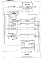
図2は、パッファ装置100の複数の周辺回路バスを接続した時の図である。
FIG. 2 is a diagram when a plurality of peripheral circuit buses of the
またバッファ装置100は、図2に示すように周波数の異なるクロックで動作する複数の周辺回路と前記複数の周辺回路を制御する制御部(ホスト)間に存在するバッファ装置として構成してもよい。
Further, as shown in FIG. 2, the
前記第1のインターフェース部は、制御部(ホスト)を接続するホストポート又はバス182として構成されるようにしてもよい。
The first interface unit may be configured as a host port or
また第2のインターフェース部は、周辺回路を接続する複数の周辺回路インターフェース回路140−0、140−1、・・、140−mを含む。 The second interface unit includes a plurality of peripheral circuit interface circuits 140-0, 140-1,..., 140-m that connect peripheral circuits.
前記バッファ110は、制御部(ホスト)と周辺装置間のアクセスに必要なアドレス及びデータの少なくとも一方を格納する。
The
ここで周辺装置からのリードデータ16は、全周辺装置バスインターフェイスからのものをまとめて図示していますが、複数が同時に有効になる事はない。
Here, the
ここでバッファ部110は、バッファとクロック制御回路を含んでいる。
Here, the
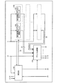
図3は図1のバッファ部110の構成図である。
FIG. 3 is a configuration diagram of the
各バッファ110−0、110−1、・・110−nはアドレスバッファ112−0、112−1、・・112−n、データバッファ114−0、114−1、・・114−n、リード/ライトフラグ116−0、116−1、・・116−n、使用フラグ118−0、118−1、・・118−nを含む。 Each of the buffers 110-0, 110-1,... 110-n includes address buffers 112-0, 112-1,... 112-n, data buffers 114-0, 114-1,. 116-n, write flags 116-0, 116-1,... 116-n, and use flags 118-0, 118-1,.
アドレスバッファ112−0、112−1、・・112−nは、メモリ空間あるいはIO空間にマッピングされたアドレスを格納するバッファで、ホストバスからのアクセス時にアドレスを格納する。 Address buffers 112-0, 112-1,... 112-n are buffers for storing addresses mapped in the memory space or IO space, and store addresses when accessed from the host bus.
データバッファ114−0、114−1、・・114−nは、アドレスバッファに対応したデータを格納するバッファであり、ホストバスからのライトアクセス時にライトデータを格納し、リードアクセス時には周辺装置からのリードデータを格納するようにしてもよい。 The data buffers 114-0, 114-1,... 114-n store data corresponding to the address buffer, store write data during write access from the host bus, and from peripheral devices during read access. You may make it store read data.
リード/ライトフラグ116−0、116−1、・・116−nは、バッファに格納したアクセスがリードかライトかを示すフラグである。 The read / write flags 116-0, 116-1,... 116-n are flags indicating whether the access stored in the buffer is read or write.
使用フラグ118−0、118−1、・・118−nは、バッファに格納したアクセスが終了したかどうかを示すフラグである。周辺装置インターフェイス部からのバッファ書き込み許可信号3−0、3−1、・・・、3−nでオフ(未使用)になる。 The use flags 118-0, 118-1,... 118-n are flags indicating whether or not the access stored in the buffer is completed. The buffer write enable signals 3-0, 3-1,..., 3-n from the peripheral device interface are turned off (not used).
クロック切り替え部120−0、120−1、・・120−nは、バッファ制御部からの周辺回路選択信号6−0、6−1、・・・、6−nによりクロックを切替える。切替えタイミングはバッファ110−0、110−1、・・110−nへの書込みが終了した時点である。 The clock switching units 120-0, 120-1,... 120-n switch clocks by peripheral circuit selection signals 6-0, 6-1,. The switching timing is when writing to the buffers 110-0, 110-1,.
バッファ部は、空バッファ指定制御部210、ネクストポインタ212、カレントポインタ214、バッファ書込み制御部216を含む。
The buffer unit includes an empty buffer
空バッファ指定制御部210は、バッファの使用フラグ118に基づき未使用のバッファをサーチしてポインタNo.を出力する。
The empty buffer
ネクストポインタ212は、空きバッファ指定制御部210が決定した次の次に使用するバッファポインターの値を格納する。
The
カレントポインタ214は、次に書込みを行うバッファのアドレスを示す。書き込み実行後はネクストポインター212の値を格納する。
The
バッファ書込み制御部216は、カレントポインター214の値により、次に書き込むバッファに対しての許可信号を生成する。
The
使用フラグ信号1は、バッファの使用フラグが出力されるもので、ホストからのアクセスで、アドレスが書き込まれた時にオンになり、周辺装置により実行されたときにオフになる。 The use flag signal 1 is a buffer use flag output, and is turned on when an address is written by an access from the host, and turned off when executed by a peripheral device.
2はリード/ライトフラグ信号であり、3−0,3−1,3−nはバッファ書込み許可信号であり、6は周辺回路選択信号であり192−0〜192−nは周辺装置のクロックであり、182はホストのクロックである。 2 is a read / write flag signal, 3-0, 3-1, and 3-n are buffer write enable signals, 6 is a peripheral circuit selection signal, and 192-0 to 192-n are clocks of peripheral devices. , And 182 is a host clock.
9はカレントポインターであり、10はホストバスからのアドレス信号であり、11はホストバスからのデータ信号であり、12はバッファからのアドレス出力信号であり、13はバッファからのデータ出力信号であり、14はホストバスからのリード/ライトフラグ入力である。 9 is a current pointer, 10 is an address signal from the host bus, 11 is a data signal from the host bus, 12 is an address output signal from the buffer, and 13 is a data output signal from the buffer. , 14 are read / write flag inputs from the host bus.
図4は周辺装置インターフェースの構成図である。 FIG. 4 is a configuration diagram of the peripheral device interface.
周辺装置インターフェースは、ポインター格納FIFO142、バッファセレクタ146、周辺装置バスインターフェイス148を含む。
The peripheral device interface includes a
ポインター格納FIFO142は、この周辺装置へのアクセスのアドレス/データが格納されたバッファNo.(ポインター)を格納するFIFOである。ポインター144とリード/ライトフラグ145の格納エリアからなる。
The
バッファセレクタ146は、ポインター格納FIFO142の出力143により、バッファを選択する。
The
周辺装置バスインターフェイス148は、周辺装置のバスへの変換を行う。アクセス終了後にポインタ格納FIFO制御用ポインタとのバッファの使用フラグをオフにする為の周辺装置アクセス実行信号17を有効にする。
Peripheral
周辺装置バッファポインター登録指示信号15は、バッファ制御部からの出力信号である。
The peripheral device buffer pointer
リードデータ16は周辺装置からのリードデータである。
The read
17は周辺装置アクセス実行信号である。 Reference numeral 17 denotes a peripheral device access execution signal.
25は周辺装置バスインターフェイスからのウエイト信号である。
図5はバッファ制御部の構成図である。 FIG. 5 is a block diagram of the buffer control unit.
バッファ制御部は、制御部152、アドレス比較部154、周辺装置登録部155を含む。
The buffer control unit includes a
周辺装置登録部155は、周辺装置のアクセス開始アドレス156と周辺装置のアクセスエリアサイズ158を含む。
The peripheral
周辺装置のアクセス開始アドレス156には、システムに搭載する周辺装置のメモリマップ上のスタートアドレスが格納される。 The peripheral device access start address 156 stores the start address on the memory map of the peripheral device mounted in the system.
周辺装置のアクセスエリアサイズ158には、システムに搭載する周辺装置のアクセスエリアサイズが格納される。
The
制御部152は、ホストからのアクセス全般の応答制御とバッファ制御を行う。
The
アドレス比較部154は、ホストからのアクセスが登録してある周辺装置に対してのものかどうかを周値と比較することで判断する。登録してある周辺装置に対してのものである周辺装置選択信号と周辺装置バッファポインター登録指示信号を有効にする。
The
19は周辺装置登録データ1であり、20は周辺装置登録データmであり、21はホストバスコマンド信号である。
22は周辺装置登録レジスタ制御信号であり、周辺装置登録部155への登録は、電源投入後のシステム初期設定時に行われる。
23はホストアクセス信号部制御信号であり、アドレスの比較は常時ではなく、ホストからのアクセスが発生した時である。ホストからのアクセスを応答制御を行う制御部152がこのタイミングを判断し、信号を生成してアドレス比較部154に指示を行う為の信号である。
24はバス制御信号であり、25はウエイト信号である。 24 is a bus control signal, and 25 is a wait signal.
図6は、周辺装置登録部に登録される周辺装置のアクセス開始アドレスと周辺装置のアクセスエリアサイズの一例である。 FIG. 6 is an example of the access start address of the peripheral device and the access area size of the peripheral device registered in the peripheral device registration unit.
本実施の形態では、システムの初期設定時に周辺装置登録部に、バッファ装置を介して接続する周辺装置の開始アドレスとエリアサイズを登録する。 In the present embodiment, the start address and area size of the peripheral device connected via the buffer device are registered in the peripheral device registration unit at the time of initial setting of the system.
本例では8個の周辺装置が接続され、アドレスとエリアサイズとして図6に示す値が登録されている。 In this example, eight peripheral devices are connected, and the values shown in FIG. 6 are registered as addresses and area sizes.
またバッファ段数は16段とする。(ポインター値 0〜FH まで)。カレントポインター0の初期値は0H、ネクストポインターの初期値は1Hとする。周辺装置インターフェイス内のFIFOの段数はバッファと同じ16段とする。 The number of buffer stages is 16. (Pointer value 0 to FH). The initial value of the current pointer 0 is 0H, and the initial value of the next pointer is 1H. The number of FIFO stages in the peripheral device interface is 16 stages, the same as the buffer.
次に、本実施の形態の並列モードによる動作の一例について説明する。 Next, an example of the operation in the parallel mode of this embodiment will be described.
まずCPUから、00A0#1000Hにデータ0000#000FH の書込みが発生したとする(ステップS1)。 First, it is assumed that data 0000 # 000FH is written to 00A0 # 1000H from the CPU (step S1).
次に制御部152がバスコマンドによりバスアクセスを認識し、信号23を有効にする。信号23が有効になる事により、バッファ書込み制御信号が動作し、カレントポインターの値が0Hである事から、信号3が有効となる。同時に、カレントポインターの値がネクストポインターの値に更新される。空きバッファ指定制御部は、バッファ1の次のバッファ2の使用フラグ118がオフである事から、ネクストポインター212に2Hをセットする(ステップS2)。
Next, the
次に信号3が有効になり、アドレスバッファ112−0に00A0#1000H が、データバッファ114−0に0000#000FHが、バッファNo.0のリード/ライトフラグ214に1が格納される。(フラグ214が1の時に書込みを表す事にする。)。バッファ0の使用フラグがオンになる(ステップS3)。
Next, the
次に書込み終了後に周辺回路選択信号6により、バッファ0のクロックが周辺装置1のクロックに切り替わる(ステップS4)。 Next, after the writing is completed, the clock of the buffer 0 is switched to the clock of the peripheral device 1 by the peripheral circuit selection signal 6 (step S4).
次にバッファ制御部150は信号23をオンにすると共に信号15有効にする。これにより周辺装置インターフェイス1のFIFOにカレントポインターの値0Hが格納される。FIFO書込みポインターが+1される。同時にFIFOに書き込まれた段の使用フラグがオンとなる(ステップS5)。
Next, the
次に周辺装置バス1が使用されていない為、即座にFIFOの値が読み出され、読出しポインターの値が+1となる。読み出されたFIFOの段の使用フラグがオフとなる(ステップS6)。 Next, since the peripheral device bus 1 is not used, the FIFO value is immediately read and the read pointer value becomes +1. The use flag of the read FIFO stage is turned off (step S6).
次にFIFOの出力によりバッファセレクタ146がバッファ0からの出力を選択し、周辺装置インターフェイスにアドレスとデータとリード/ライトフラグが出力され、周辺装置1へのアクセスが開始される。周辺装置アクセス実行信号17がアクティブとなり、FIFOの出力とともにバッファ部に送信され、FIFOの出力値が示すバッファの使用フラグ118がオフとなる。これにあわせてバッファの動作クロックがCPUバスクロックに戻る。バッファからのアドレスは、周辺装置バスに合わせたものに変換されてもよい(ステップS7)。
Next, the
CPUからのアクセスは、ライト動作の場合、バッファへの書込みが終了した時点でCPUバスのサイクルを終了させる。既にバッファに書き込まれたアクセスの実際の周辺装置への書込みを待たずにバスサイクルを終了させる。リード動作の場合は、このリード動作が終了した時点でCPUバスのサイクルを終了させる(ステップS8)。 In the case of a write operation, the access from the CPU ends the cycle of the CPU bus when the writing to the buffer is completed. The bus cycle is terminated without waiting for the write of the access already written in the buffer to the actual peripheral device. In the case of a read operation, the CPU bus cycle is terminated when the read operation is completed (step S8).
次にCPUバスからのライトアクセスは、上記の動作を繰り返し、バッファが一杯になるまでは、CPUからのアクセス順序に関係なく、周辺装置に対してのアクセスが実行される。使用したバッファは次々に処理フラグ118がオフになり開放されて、次のCPUUからのアクセス情報が格納される。空きバッファ指定制御部210が各バッファの使用フラグeをバッファNo.を+1方向にチェックし、ネクストポインター212を更新する(ステップS9)。
Next, in the write access from the CPU bus, the above operation is repeated, and until the buffer is full, access to the peripheral device is executed regardless of the access order from the CPU. The used buffer is successively released when the processing flag 118 is turned off, and the access information from the next CPUU is stored. The empty buffer
図7は並列モードの場合の処理の流れを示すフローチャートである。 FIG. 7 is a flowchart showing the flow of processing in the parallel mode.
ホストCPUからAポートに書込み動作発生(ステップS110)。ここでAポートとは周辺装置Aが接続されているポートである。 A write operation occurs from the host CPU to the A port (step S110). Here, the A port is a port to which the peripheral device A is connected.
ポインター001のバッファにアドレス・データを保存。ホストCPUへはアクセス終了を報告。この時点ではポインター001のバッファはホストCPUのクロックで動作している(ステップS120)。 Address data is stored in the pointer 001 buffer. Report the end of access to the host CPU. At this time, the buffer of the pointer 001 is operating with the clock of the host CPU (step S120).
ポインター001のクロックがAポートのクロックに切り替わると共に、ポインター値001がAポートのポインターFIFOに格納される。Aポートのアクセス終了後、バッファはホストCPU側クロックに切り替わる(ステップS130)。 The clock of the pointer 001 is switched to the clock of the A port, and the pointer value 001 is stored in the pointer FIFO of the A port. After the access to the A port is completed, the buffer is switched to the host CPU side clock (step S130).
ポインター002のバッファにアドレス・データを保存。ホストCPUへはアクセス終了を報告(ステップS140)。 Address data is saved in the buffer of pointer 002. Report the end of access to the host CPU (step S140).
ポインター002のクロックがAポートのクロックに切り替わると共に、ポインター値002がAポートのポインターFIFOに格納される。Aポートのアクセス終了後、ホストCPU側クロックに切り替わる(ステップS160)。 The clock of the pointer 002 is switched to the clock of the A port, and the pointer value 002 is stored in the pointer FIFO of the A port. After the A port access is completed, the host CPU side clock is switched (step S160).
ホストCPUからBポートに書込み動作発生(ステップS170)。ここでBポートとは周辺装置Bが接続されているポートである。 A write operation occurs from the host CPU to the B port (step S170). Here, the B port is a port to which the peripheral device B is connected.
ポインター003のバッファにアドレスデータを保存。ホストCPUへはアクセス終了を報告。この時点ではポインター003のバッファはホストCPUのクロックで動作している(ステップS180)
ポインター003のクロックがBポートのクロックに切り替わると共に、ポインター値003がBポートのポインターFIFOに格納される。Bポートのアクセス終了後ホストCPU側クロックに切り替わる(ステップS190)
ホストCPUからAポートに書込み動作発生(ステップS200)。
Address data is saved in the buffer of pointer 003. Report the end of access to the host CPU. At this time, the buffer of the pointer 003 is operating with the clock of the host CPU (step S180).
The clock of the pointer 003 is switched to the clock of the B port, and the pointer value 003 is stored in the pointer FIFO of the B port. After the B port access is completed, the host CPU side clock is switched (step S190).
A write operation occurs from the host CPU to the A port (step S200).
ポインター004のバッファにアドレス・データを保存。ホストCPUへはアクセス終了を報告(ステップS210)。 Address data is stored in the pointer 004 buffer. Report the end of access to the host CPU (step S210).
ポインター004のクロックがAポートのクロックに切り替わると共に、ポインター値004がAポートのポインターFIFOに格納される。Aポートのアクセス終了後、ホストCPU側クロックに切り替わる(ステップS220)。 The clock of the pointer 004 is switched to the clock of the A port, and the pointer value 004 is stored in the pointer FIFO of the A port. After the A port access is completed, the host CPU side clock is switched (step S220).
ホストCPUからAポートに読出し動作発生(ステップS230)。 A read operation occurs from the host CPU to the A port (step S230).
ポインター005のアドレスバッファにアドレスを保存(ステップS240)。 The address is stored in the address buffer of the pointer 005 (step S240).
ポインター005のクロックがAポートのクロックに切り替わると共に、ポインター値005がAポートのポインターFIFOに格納される(ステップS250)。 The clock of the pointer 005 is switched to the clock of the A port, and the pointer value 005 is stored in the pointer FIFO of the A port (step S250).
ポインター005のデータバッファにAポートからの読出しデータが格納された後、ホストCPUのクロックに切り替わる(ステップS260)。 After the data read from the A port is stored in the data buffer of the pointer 005, the clock is switched to the host CPU (step S260).
ホストCPUへ読出しデータと共にアクセス終了信号が返される(ステップS270)。 An access end signal is returned to the host CPU together with the read data (step S270).
なおステップS190において、これ以前の他のポートのアクセスが終了した後にポートアクセスが許可されるように制御することで逐次モード(ホストからのアクセスの順番に処理を実行するモード)の処理を実現することができる。 In step S190, sequential mode (a mode in which processing is executed in the order of access from the host) is realized by performing control so that port access is permitted after access of other ports before this is completed. be able to.
逐次的動作モードに設定すると実質的アクセス順番が保証できる。 When the sequential operation mode is set, a substantial access order can be guaranteed.
並列的動作モードに設定すると各周辺回路へのアクセスが平行して行われるのでシステムのパフォーマンスを上げる事ができる。ホストCPU側の動作クロックと周辺回路側の動作クロックが著しく異なりホスト側が速い場合に効果は顕著である。 When the parallel operation mode is set, access to each peripheral circuit is performed in parallel, so that the system performance can be improved. The effect is remarkable when the operation clock on the host CPU side and the operation clock on the peripheral circuit side are significantly different and the host side is fast.
逐次処理の場合は、ホスト側CPUが高速に動作しても遅い周辺回路のアクセスが終わるまでは次の動作に進めないが、並列モードの場合は、バッファに高速に書き込んでしまえば遅い周辺回路のアクセスが終了しなくても別な周辺回路にアクセスする事が可能となる。 In the case of sequential processing, even if the host side CPU operates at high speed, it cannot proceed to the next operation until the access of the slow peripheral circuit is completed. It is possible to access another peripheral circuit without completing the access.
従って各周辺回路間の連携制御が無い場合は、並列モードにする事で、各周辺回路を実質並列制御する事が可能となるのでシステム性能の向上に繋がる。 Accordingly, when there is no cooperative control between the peripheral circuits, the parallel mode can be achieved by controlling each peripheral circuit in parallel, leading to an improvement in system performance.
なお、本発明は本実施形態に限定されず、本発明の要旨の範囲内で種々の変形実施が可能である。 In addition, this invention is not limited to this embodiment, A various deformation | transformation implementation is possible within the range of the summary of this invention.
100 バッファ装置、 110 バッファ、120 クロック切り替え部、130 第1のI/F部、140 第2のI/F部、142 FIFO、146 セレクタ、148 バスドライバレシーバ、150 クロック切り替え制御部、152 クロック切り替え制御信号、170 制御部、180 第1の回路、190 第2の回路、300 情報処理装置 100 buffer device, 110 buffer, 120 clock switching unit, 130 first I / F unit, 140 second I / F unit, 142 FIFO, 146 selector, 148 bus driver receiver, 150 clock switching control unit, 152 clock switching Control signal, 170 control unit, 180 first circuit, 190 second circuit, 300 information processing apparatus
Claims (14)
第1の回路と第2の回路のデータのやり取りに必要なアドレス及びデータの少なくとも一方を格納するバッファと、
第1の回路とバッファの接続部である第1のインターフェース部と、
第2の回路とバッファの接続部である第2のインターフェース部と、
第1の回路及び第2の回路のバッファへのアクセス状況に基づき、前記バッファに供給するクロックを切り替えるタイミングを判断し、バッファに供給するクロックの選択または切り替えを指示するためのクロック切り替え制御信号を生成するクロック切り替え制御回路と、
第1の回路の動作クロック及び第2の回路の動作クロックを含む複数のクロックを入力し、前記クロック切り替え信号に基づきいずれかのクロックを選択して前記バッファに供給するクロック切り替え回路と、
を含むことを特徴とするバッファ装置。 A buffer device that exists between a first circuit and a second circuit that operate with clocks having different frequencies,
A buffer for storing at least one of an address and data necessary for data exchange between the first circuit and the second circuit;
A first interface unit which is a connection unit between the first circuit and the buffer;
A second interface unit that is a connection between the second circuit and the buffer;
Based on the access status to the buffers of the first circuit and the second circuit, the timing for switching the clock supplied to the buffer is determined, and a clock switching control signal for instructing selection or switching of the clock supplied to the buffer is provided. A clock switching control circuit to be generated;
A clock switching circuit that receives a plurality of clocks including an operation clock of the first circuit and an operation clock of the second circuit, selects one of the clocks based on the clock switching signal, and supplies the selected clock to the buffer;
A buffer device comprising:
前記バッファは、
複数段で構成されており、
前記クロック切り替え制御回路は、
第1の回路及び第2の回路の各段のバッファへのアクセス状況に基づき、前記各段のバッファに供給するクロックを切り替えるタイミングを判断し、各段に対応したクロック切り替え制御信号を生成し、
前記クロック切り替え回路は、
前記バッファの格段に対応して第1の回路の動作クロック及び第2の回路の動作クロックを含む複数のクロックを入力し、前記各段に対応したクロック切り替え信号に基づきいずれかのクロックを選択して各段のバッファに供給することを特徴とするバッファ装置。 In claim 1,
The buffer is
It consists of multiple stages,
The clock switching control circuit includes:
Based on the access status to the buffer of each stage of the first circuit and the second circuit, the timing to switch the clock supplied to the buffer of each stage is determined, and a clock switching control signal corresponding to each stage is generated,
The clock switching circuit is
A plurality of clocks including an operation clock of the first circuit and an operation clock of the second circuit are input corresponding to the exceptional level of the buffer, and one of the clocks is selected based on the clock switching signal corresponding to each stage. A buffer device for supplying to each stage buffer.
前記第2のインターフェース部は、
第1の回路のバッファへの書き込みが発生すると書き込みのあった段のバッファへのポインターを格納するためのFIFOを含み、
前記FIFOの出力順に先入先出で第2の回路からバッファへのアクセスを許可するように制御することを特徴とするバッファ装置。 In claim 2,
The second interface unit includes:
A FIFO for storing a pointer to the buffer at the stage of writing when writing to the buffer of the first circuit occurs;
A buffer device, wherein control is performed to permit access to the buffer from the second circuit in first-in first-out order in the output order of the FIFO.
前記バッファ装置は、
周波数の異なるクロックで動作する複数の周辺回路と前記複数の周辺回路を制御する制御部の間に存在するバッファ装置であって、
前記第1のインターフェース部は、
前記制御部を接続するホストポート又はバスとして構成され、
前記第2のインターフェース部は
前記複数の周辺回路に対応する複数の周辺回路インターフェース回路含み、
前記バッファは、
制御部と周辺装置間のアクセスに必要なアドレス及びデータの少なくとも一方を格納することを特徴とするバッファ装置。 In any one of Claims 2 thru | or 3.
The buffer device includes:
A buffer device that exists between a plurality of peripheral circuits that operate with clocks having different frequencies and a control unit that controls the plurality of peripheral circuits,
The first interface unit includes:
It is configured as a host port or bus that connects the control unit,
The second interface unit includes a plurality of peripheral circuit interface circuits corresponding to the plurality of peripheral circuits,
The buffer is
A buffer device for storing at least one of an address and data necessary for access between a control unit and a peripheral device.
前記各周辺回路インターフェース回路は、
各周辺回路毎に、第1の回路のバッファへの当該周辺回路に対する書き込みが発生すると書き込みのあった段のバッファへのポインターを格納するためのFIFOを含み、前記FIFOの出力順に先入先出で当該周辺回路からバッファへのアクセスを許可するように制御することを特徴とするバッファ装置。 In claim 4,
Each of the peripheral circuit interface circuits is
Each peripheral circuit includes a FIFO for storing a pointer to the buffer at the stage where writing has been performed when writing to the buffer of the first circuit occurs in the buffer of the first circuit. A buffer device that controls to permit access to the buffer from the peripheral circuit.
前記各周辺回路は他の周辺回路とは独立したバスを有しており、
前記各周辺回路インターフェース回路は、
対応する周辺回路のバスに接続されていることを特徴とするバッファ装置。 In any of claims 4 to 5,
Each peripheral circuit has a bus independent of other peripheral circuits,
Each of the peripheral circuit interface circuits is
A buffer device connected to a bus of a corresponding peripheral circuit.
前記クロック切り替え制御回路は、
第1の回路のバッファへの書き込みの終了を検出したら、当該バッファへ供給するクロックを、第2の回路の動作クロックに切り替えるように指示するクロック切り替え制御信号を生成することを特徴とするバッファ装置。 In any one of Claims 1 thru | or 6.
The clock switching control circuit includes:
When the end of writing to the buffer of the first circuit is detected, a buffer device that generates a clock switching control signal that instructs to switch the clock supplied to the buffer to the operation clock of the second circuit .
前記バッファは、
バッファに書き込まれた内容が第2の回路に対する読み出し又は書き込みのいずれであるかを識別するためのR/W識別フラグを含み、
前記クロック切り替え制御回路は、
R/W識別フラグが書き込みを示している場合には、バッファの内容が第2の回路から読み出されたことを検出したら、当該バッファへ供給するクロックを第1の回路の動作クロックに切り替えるように指示するクロック切り替え制御信号を生成することを特徴とするバッファ装置。 In any one of Claims 1 thru | or 7,
The buffer is
An R / W identification flag for identifying whether the content written in the buffer is a read or write to the second circuit;
The clock switching control circuit includes:
When the R / W identification flag indicates writing, when it is detected that the buffer contents have been read from the second circuit, the clock supplied to the buffer is switched to the operation clock of the first circuit. A buffer switching control signal for instructing
前記バッファは、
バッファに書き込まれた内容が第2の回路に対する読み出し又は書き込みのいずれであるかを識別するためのR/W識別フラグを含み、
前記クロック切り替え制御回路は、
R/W識別フラグが読み出しを示している場合には、第2の回路からバッファへの書き込みが行われたことを検出したら、当該バッファへ供給するクロックを、第1の回路の動作クロックに切り替えるように指示するクロック切り替え制御信号を生成することを特徴とするバッファ装置。 In any one of Claims 1 thru | or 8.
The buffer is
An R / W identification flag for identifying whether the content written in the buffer is a read or write to the second circuit;
The clock switching control circuit includes:
When the R / W identification flag indicates reading, when it is detected that writing from the second circuit to the buffer has been performed, the clock supplied to the buffer is switched to the operation clock of the first circuit. A buffer device that generates a clock switching control signal instructing
前記バッファは、
バッファに書き込まれた内容が第2の回路に対する読み出し又は書き込みのいずれであるかを識別するためのR/W識別フラグを含み、
前記クロック切り替え制御回路は、
R/W識別フラグが読み出しを示している場合には、第2の回路から読み出し終了を検出したら、バッファを介さず直接第1の回路へ読み出したデータを出力し、当該バッファへ供給するクロックを、第1の回路の動作クロックに切り替えるように指示するクロック切り替え制御信号を生成することを特徴とするバッファ装置。 In any one of Claims 1 thru | or 8.
The buffer is
An R / W identification flag for identifying whether the content written in the buffer is a read or write to the second circuit;
The clock switching control circuit includes:
When the R / W identification flag indicates reading, when the end of reading is detected from the second circuit, the read data is output directly to the first circuit without passing through the buffer, and the clock supplied to the buffer is supplied. A buffer device for generating a clock switching control signal for instructing to switch to the operation clock of the first circuit.
逐次モードであるか並列モードであるかの情報が記憶されるモード設定レジスタと、
モード設定レジスタの値が逐次モードであることを示している場合には第1の回路からのアクセスの順番に処理を実行するように制御し、モード設定レジスタの値が並列モードであることを示している場合には第1の回路からのアクセスの順番によらず処理を実行するように制御する回路と、を含み、
前記モード設定レジスタの値は第1の回路からの指示信号に基づき設定されることを特徴とするバッファ装置。 In any one of Claims 1 to 10,
A mode setting register for storing information on whether the mode is the sequential mode or the parallel mode;
When the value of the mode setting register indicates the sequential mode, control is performed so that the processing is executed in the order of access from the first circuit, and the value of the mode setting register indicates the parallel mode. And a circuit that controls to execute the process regardless of the order of access from the first circuit,
The buffer device characterized in that the value of the mode setting register is set based on an instruction signal from the first circuit.
第1の回路及び第2の回路のバッファへのアクセス状況に基づき、前記バッファに供給するクロックを切り替えるタイミングを判断し、バッファに供給するクロックの選択または切り替えを指示するためのクロック切り替え制御信号を生成するステップと、
第1の回路の動作クロック及び第2の回路の動作クロックを含む複数のクロックを入力し、前記クロック切り替え信号に基づきいずれかのクロックを選択して前記バッファに供給するステップとを、
を含むことを特徴とするバッファ装置の制御方法。 A buffer that exists between a first circuit and a second circuit that operate with clocks having different frequencies and stores at least one of an address and data necessary for data exchange between the first circuit and the second circuit; A control method for a buffer device, comprising:
Based on the access status to the buffers of the first circuit and the second circuit, the timing for switching the clock supplied to the buffer is determined, and a clock switching control signal for instructing selection or switching of the clock supplied to the buffer is provided. Generating step;
Inputting a plurality of clocks including an operation clock of the first circuit and an operation clock of the second circuit, selecting any one of the clocks based on the clock switching signal, and supplying the selected clock to the buffer;
A control method for a buffer device.
前記第1の回路からの指示信号に基づき実行モードを設定するステップと、
実行モードが逐次モードに設定されている場合には第1の回路からのアクセスの順番に処理を実行するように制御し、並列モードに設定されている場合には第1の回路からのアクセスの順番によらず処理を実行するように制御するステップと、
を含むことを特徴とするバッファ装置の制御方法。
In claim 13,
Setting an execution mode based on an instruction signal from the first circuit;
When the execution mode is set to the sequential mode, control is performed so that processing is executed in the order of access from the first circuit. When the execution mode is set to the parallel mode, access from the first circuit is controlled. A step for controlling the processing to be executed regardless of the order; and
A control method for a buffer device.
Priority Applications (1)
| Application Number | Priority Date | Filing Date | Title |
|---|---|---|---|
| JP2006045374A JP2007109199A (en) | 2005-09-15 | 2006-02-22 | Buffer device, control method for buffer device, and information processor |
Applications Claiming Priority (2)
| Application Number | Priority Date | Filing Date | Title |
|---|---|---|---|
| JP2005268628 | 2005-09-15 | ||
| JP2006045374A JP2007109199A (en) | 2005-09-15 | 2006-02-22 | Buffer device, control method for buffer device, and information processor |
Publications (1)
| Publication Number | Publication Date |
|---|---|
| JP2007109199A true JP2007109199A (en) | 2007-04-26 |
Family
ID=38034999
Family Applications (1)
| Application Number | Title | Priority Date | Filing Date |
|---|---|---|---|
| JP2006045374A Withdrawn JP2007109199A (en) | 2005-09-15 | 2006-02-22 | Buffer device, control method for buffer device, and information processor |
Country Status (1)
| Country | Link |
|---|---|
| JP (1) | JP2007109199A (en) |
Cited By (2)
| Publication number | Priority date | Publication date | Assignee | Title |
|---|---|---|---|---|
| JP2011519077A (en) * | 2008-02-20 | 2011-06-30 | ヒューレット−パッカード デベロップメント カンパニー エル.ピー. | Redriver having two reference clocks and operation method thereof |
| JP2015043170A (en) * | 2013-08-26 | 2015-03-05 | 株式会社東芝 | Interface circuit and system |
-
2006
- 2006-02-22 JP JP2006045374A patent/JP2007109199A/en not_active Withdrawn
Cited By (2)
| Publication number | Priority date | Publication date | Assignee | Title |
|---|---|---|---|---|
| JP2011519077A (en) * | 2008-02-20 | 2011-06-30 | ヒューレット−パッカード デベロップメント カンパニー エル.ピー. | Redriver having two reference clocks and operation method thereof |
| JP2015043170A (en) * | 2013-08-26 | 2015-03-05 | 株式会社東芝 | Interface circuit and system |
Similar Documents
| Publication | Publication Date | Title |
|---|---|---|
| US20020095562A1 (en) | Arithmetic unit comprising a memory shared by a plurality of processors | |
| US7724984B2 (en) | Image processing apparatus | |
| JPH11250228A (en) | Picture processor and system therefor | |
| JP2008276638A (en) | Semiconductor storage device, memory access control system and method for reading data | |
| CN101243416A (en) | Apparatus and method for storing data and/or instructions in a computer system having at least two processing units and at least one first memory or memory area for data and/or instructions | |
| JP4388005B2 (en) | Context switching device | |
| US9984014B2 (en) | Semiconductor device | |
| KR100631778B1 (en) | Data buffer circuit, interface circuit and control method thereof | |
| JP2008009591A (en) | Cache memory system | |
| JPWO2011099048A1 (en) | Transmission control device, memory control device, and PLC including the transmission control device | |
| JP2007109199A (en) | Buffer device, control method for buffer device, and information processor | |
| US8533368B2 (en) | Buffering device and buffering method | |
| JP3505728B2 (en) | Storage controller | |
| US4547848A (en) | Access control processing system in computer system | |
| JP2006164070A5 (en) | ||
| US20050135402A1 (en) | Data transfer apparatus | |
| JP4327238B2 (en) | System controller and cache control method | |
| US6681273B1 (en) | High performance, variable data width FIFO buffer | |
| US20050223129A1 (en) | Arbitration of data transfer requests | |
| JP2005107873A (en) | Semiconductor integrated circuit | |
| JP2009199384A (en) | Data processing apparatus | |
| JP2004005710A (en) | Information processor | |
| US20100153610A1 (en) | Bus arbiter and bus system | |
| JPH1185673A (en) | Method and device for controlling shared bus | |
| JP6535516B2 (en) | Multi-programmable device system and control method thereof |
Legal Events
| Date | Code | Title | Description |
|---|---|---|---|
| RD04 | Notification of resignation of power of attorney |
Free format text: JAPANESE INTERMEDIATE CODE: A7424 Effective date: 20080627 |
|
| A300 | Withdrawal of application because of no request for examination |
Free format text: JAPANESE INTERMEDIATE CODE: A300 Effective date: 20090512 |