JP2007108228A - Photoelectric consolidated substrate and its manufacturing method - Google Patents
Photoelectric consolidated substrate and its manufacturing method Download PDFInfo
- Publication number
- JP2007108228A JP2007108228A JP2005296571A JP2005296571A JP2007108228A JP 2007108228 A JP2007108228 A JP 2007108228A JP 2005296571 A JP2005296571 A JP 2005296571A JP 2005296571 A JP2005296571 A JP 2005296571A JP 2007108228 A JP2007108228 A JP 2007108228A
- Authority
- JP
- Japan
- Prior art keywords
- thin film
- opto
- metal thin
- core layer
- cladding layer
- Prior art date
- Legal status (The legal status is an assumption and is not a legal conclusion. Google has not performed a legal analysis and makes no representation as to the accuracy of the status listed.)
- Pending
Links
Images


Abstract
Description
本発明は、一つの基板に光導波路(光配線)と金属製配線パターン(電気配線)とが形成されている光電気混載基板およびその製造方法に関するものである。 The present invention relates to an opto-electric hybrid board in which an optical waveguide (optical wiring) and a metal wiring pattern (electric wiring) are formed on one substrate, and a method for manufacturing the same.
最近、光を媒体とした情報通信が普及している。そこで、情報通信用電子機器等に用いる基板として、光導波路(光配線)と金属製配線パターン(電気配線)とが形成されている光電気混載基板(例えば、特許文献1参照)が採用されている。 Recently, information communication using light as a medium has become widespread. Therefore, an opto-electric hybrid board (for example, see Patent Document 1) in which an optical waveguide (optical wiring) and a metal wiring pattern (electric wiring) are formed is employed as a board used for information communication electronic devices and the like. Yes.
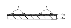
この光電気混載基板は、図9に示すように、金属製配線パターン11が形成された基板50と、光導波路2とが、接着剤層60を介して接着されて形成されている。この光電気混載基板には、通常、上記金属製配線パターン11上に、電気信号を光信号Lに変換する発光素子Aと、光信号Lを電気信号に変換する受光素子Bとが接続されている。そして、発光素子Aからの光信号Lを、光導波路を介して受光素子Bに伝達できるよう、発光素子Aの下方および受光素子Bの下方では、上記基板50に貫通孔51が形成され、かつ、コア層2bに光路変換ミラー21が形成されている。この光路変換ミラー21は、コア層2bに形成された、光軸に対して45°傾斜した傾斜面である。
As shown in FIG. 9, this opto-electric hybrid board is formed by bonding a
そして、光信号Lの伝達は、発光素子Aから下方に発せられた光信号Lを、一方(図9では左側)の光路変換ミラー(傾斜面)21で反射させて(光路を90°変換させて)、光導波路2のコア層2b内に導き、再度、他方(図9では右側)の光路変換ミラー(傾斜面)21で反射させて(光路を90°変換させて)、上方の受光素子Bに伝達させることにより行われる。なお、図9において、2aは第1クラッド層、2cは第2クラッド層である。
しかしながら、信号の高密度化および高速化に伴って、従来の光電気混載基板では、光信号Lの伝搬効率が不充分になってきている。 However, with the increase in the density and speed of signals, the propagation efficiency of the optical signal L has become insufficient in the conventional opto-electric hybrid board.
そこで、本発明者は、この原因について研究を重ねた結果、その原因は、特に、光導波路2のコア層2bと受光素子Bとの間で光信号Lが減衰することにあることを突き止めた。そして、その減衰する原因は、光導波路2のコア層2bと受光素子Bとの間の距離が長いことにあることも突き止めた。
Therefore, as a result of repeated research on this cause, the present inventor has found that the cause is that the optical signal L is attenuated particularly between the
この原因究明結果に基づいて、本発明者は、光導波路2のコア層2bと受光素子Bとの間の距離(コア層2bと金属製配線パターン11の表面との間の距離)を短縮すべく、金属製配線パターン11が形成された基板50を用いない光電気混載基板の製造方法を考えた。この製造方法は、金属箔等の金属シートの片面に光導波路2を形成した後、上記金属シートをエッチングすることにより、所定の金属製配線パターン11に形成する方法である。
Based on the cause investigation result, the inventor shortens the distance between the
しかしながら、この製造方法では、金属シートの厚みをある程度厚くしなければ、製造過程における金属シートの取り扱い性が悪く、光導波路2および金属製配線パターン11を形成する際の作業性が悪かった。そこで、金属シートの取り扱い性をよくするために金属シートを厚くすると、金属製配線パターン11も厚くなるため、今度は光導波路2のコア層2bと受光素子Bとの間の距離が充分に短縮されず、光信号Lの伝搬効率を充分に向上させることができないという問題が生じた。
However, in this manufacturing method, unless the thickness of the metal sheet is increased to some extent, the handleability of the metal sheet in the manufacturing process is poor, and the workability when forming the
本発明は、このような事情に鑑みなされたもので、光導波路のコア層と金属製配線パターン表面との間の距離を充分に短縮し、光信号の伝搬効率を充分に向上させることができる光電気混載基板およびその製造方法の提供をその目的とする。 The present invention has been made in view of such circumstances, and can sufficiently shorten the distance between the core layer of the optical waveguide and the surface of the metal wiring pattern and sufficiently improve the propagation efficiency of the optical signal. An object is to provide an opto-electric hybrid board and a manufacturing method thereof.
上記の目的を達成するため、本発明は、光信号伝達手段と、電気信号伝達手段とを有した光電気混載基板であって、上記光信号伝達手段が、第1クラッド層と第2クラッド層とでコア層を挟持するとともに被包し、そのコア層の所定位置を光路変換ミラーに形成してなる光導波路からなり、上記電気信号伝達手段が、上記第1クラッド層の表面に絶縁層を介さず直接形成した金属製配線パターンからなる光電気混載基板を第1の要旨とする。 In order to achieve the above object, the present invention provides an opto-electric hybrid board having optical signal transmission means and electrical signal transmission means, wherein the optical signal transmission means includes a first cladding layer and a second cladding layer. The core layer is sandwiched and encapsulated, and a predetermined position of the core layer is formed on an optical path conversion mirror, and the electric signal transmission means includes an insulating layer on the surface of the first cladding layer. An opto-electric hybrid board made of a metal wiring pattern directly formed without any intervention is taken as a first gist.
また、本発明は、上記光電気混載基板を製造する方法であって、剥離基材の表面に金属薄膜が形成された金属薄膜転写シートを準備し、その金属薄膜の表面に第1クラッド層を形成する工程と、上記剥離基材を金属薄膜から剥離する工程と、上記金属薄膜をエッチングにより所定の配線パターンに形成する工程と、上記第1クラッド層の表面にコア層を形成する工程と、このコア層の表面を覆うように第2クラッド層を形成する工程と、上記コア層の所定位置を光路変換ミラーに形成する工程とを備えている光電気混載基板の製造方法を第2の要旨とする。 The present invention is also a method for producing the opto-electric hybrid board, comprising preparing a metal thin film transfer sheet in which a metal thin film is formed on the surface of a release substrate, and providing a first cladding layer on the surface of the metal thin film. A step of forming, a step of peeling the release substrate from the metal thin film, a step of forming the metal thin film into a predetermined wiring pattern by etching, a step of forming a core layer on the surface of the first cladding layer, A second summary of a method for manufacturing an opto-electric hybrid board, comprising: a step of forming a second cladding layer so as to cover the surface of the core layer; and a step of forming a predetermined position of the core layer on an optical path conversion mirror. And
本発明者は、先の考えた光電気混載基板の製造方法での結果に基づき、さらに研究を重ねた。その結果、光電気混載基板の製造方法において、剥離基材の表面に金属薄膜が形成された金属薄膜転写シートを用い、その金属薄膜の表面に第1クラッド層を形成した後に、上記剥離基材を金属薄膜から剥離し、上記金属薄膜をエッチングにより所定の配線パターンに形成すると、作業性がよく、品質の安定した光電気混載基板を製造することができ、しかも、コア層と配線パターン表面との間の距離を充分に短縮できることを見出し、本発明に到達した。 The inventor conducted further research based on the result of the above-described method for manufacturing an opto-electric hybrid board. As a result, in the method for manufacturing an opto-electric hybrid board, a metal thin film transfer sheet having a metal thin film formed on the surface of the peeling base material is used, and after forming the first cladding layer on the surface of the metal thin film, the peeling base material If the metal thin film is peeled off from the metal thin film and the metal thin film is formed into a predetermined wiring pattern by etching, an opto-electric hybrid board with good workability and stable quality can be manufactured. The present inventors have found that the distance between the two can be sufficiently shortened, and have reached the present invention.
すなわち、剥離基材の表面に金属薄膜が形成された上記金属薄膜転写シートを用いると、その金属薄膜を厚くしなくても、剥離基材により、ある程度の剛性を有しているため、金属薄膜転写シートの取り扱い性がよくなっている。これにより、その金属薄膜転写シートの金属薄膜の表面に第1クラッド層を形成する際の作業性がよくなっている。そして、剥離基材を剥離しても、上記金属薄膜と第1クラッド層との積層体は、第1クラッド層の形成により、ある程度の剛性を得ることができ、取り扱い性がよくなっている。このため、その後の工程(金属薄膜をエッチングにより所定の配線パターンに形成する工程,第1クラッド層表面にコア層を形成する工程等)でも、作業性がよく、その結果、品質の安定した光電気混載基板を得ることができる。そして、その得られた光電気混載基板は、従来の光電気混載基板を構成する、コア層上方の基板(金属製配線パターンが形成された基板)がなく、しかも、配線パターン(金属薄膜)の厚みも薄くできるため、その配線パターン上に接続される受光素子と光導波路のコア層との間の距離を充分に短縮することができ、光信号の伝搬効率を充分に向上させることができる。 That is, when the metal thin film transfer sheet having the metal thin film formed on the surface of the peeling substrate is used, the metal thin film has a certain degree of rigidity even if the metal thin film is not thickened. The transfer sheet is easy to handle. Thereby, the workability | operativity at the time of forming a 1st clad layer on the surface of the metal thin film of the metal thin film transfer sheet is improving. And even if it peels a peeling base material, the laminated body of the said metal thin film and 1st cladding layer can acquire a certain amount of rigidity by formation of a 1st cladding layer, and the handleability is improving. For this reason, in subsequent processes (such as a process of forming a metal thin film into a predetermined wiring pattern by etching, a process of forming a core layer on the surface of the first cladding layer, etc.) An electric mixed substrate can be obtained. The obtained opto-electric hybrid board does not have a substrate above the core layer (a board on which a metal wiring pattern is formed) that constitutes a conventional opto-electric hybrid board, and the wiring pattern (metal thin film) Since the thickness can be reduced, the distance between the light receiving element connected on the wiring pattern and the core layer of the optical waveguide can be sufficiently shortened, and the propagation efficiency of the optical signal can be sufficiently improved.
本発明の光電気混載基板は、金属製配線パターンが、光導波路の第1クラッド層の表面に絶縁層を介さず直接形成されているため、光導波路のコア層と金属製配線パターン表面との間の距離が充分に短縮されている。その結果、上記配線パターン上に接続される受光素子と光導波路のコア層との間の距離を充分に短縮することができ、光信号の伝搬効率を充分に向上させることができる。 In the opto-electric hybrid board according to the present invention, the metal wiring pattern is directly formed on the surface of the first cladding layer of the optical waveguide without an insulating layer, so that the core layer of the optical waveguide and the surface of the metal wiring pattern The distance between them is sufficiently shortened. As a result, the distance between the light receiving element connected on the wiring pattern and the core layer of the optical waveguide can be sufficiently shortened, and the propagation efficiency of the optical signal can be sufficiently improved.
特に、上記金属製配線パターンの厚みが、1.0〜5.0μmの範囲内である場合には、その金属製配線パターンの厚みが充分に薄いため、光信号の伝搬効率をより一層向上させることができる。 In particular, when the thickness of the metal wiring pattern is in the range of 1.0 to 5.0 μm, the thickness of the metal wiring pattern is sufficiently thin, so that the propagation efficiency of the optical signal is further improved. be able to.
また、本発明の光電気混載基板の製造方法は、後に所定の配線パターンに形成される金属薄膜が剥離基材の表面に形成されている金属薄膜転写シートを用いるため、その金属薄膜転写シートを、ある程度の剛性を有した状態で取り扱うことができる。このため、その金属薄膜転写シートの金属薄膜(配線パターン)を薄くすることができる。また、その金属薄膜の表面に第1クラッド層を形成するため、金属薄膜転写シートの剥離基材を剥離しても、金属薄膜と第1クラッド層との積層体は、その第1クラッド層により、ある程度の剛性を得ることができ、取り扱い性がよくなっている。このため、その後の工程では、作業性がよく、その結果、品質の安定した光電気混載基板を得ることができる。そして、その得られた光電気混載基板では、配線パターンが、光導波路の第1クラッド層の表面に絶縁層を介さず直接形成されているため、光導波路のコア層と配線パターン表面との間の距離を充分に短縮することができる。その結果、上記配線パターン上に接続される受光素子と光導波路のコア層との間の距離を充分に短縮することができ、光信号の伝搬効率を充分に向上させることができる。 In addition, the method for manufacturing an opto-electric hybrid board according to the present invention uses a metal thin film transfer sheet in which a metal thin film to be formed later on a predetermined wiring pattern is formed on the surface of a release substrate. , It can be handled with a certain degree of rigidity. For this reason, the metal thin film (wiring pattern) of the metal thin film transfer sheet can be made thin. In addition, since the first clad layer is formed on the surface of the metal thin film, even if the peeling substrate of the metal thin film transfer sheet is peeled off, the laminate of the metal thin film and the first clad layer is formed by the first clad layer. A certain degree of rigidity can be obtained, and the handleability is improved. For this reason, in a subsequent process, workability | operativity is good, As a result, the opto-electric hybrid board | substrate with stable quality can be obtained. In the obtained opto-electric hybrid board, the wiring pattern is formed directly on the surface of the first cladding layer of the optical waveguide without an insulating layer, and therefore, between the core layer of the optical waveguide and the surface of the wiring pattern. Can be sufficiently shortened. As a result, the distance between the light receiving element connected on the wiring pattern and the core layer of the optical waveguide can be sufficiently shortened, and the propagation efficiency of the optical signal can be sufficiently improved.
特に、上記金属薄膜の厚みが、1.0〜5.0μmの範囲内である場合には、後に形成される配線パターンの厚みを充分に薄くすることができ、しかも、剥離基材を剥離した後の、金属薄膜と第1クラッド層との積層体を、ある程度の剛性を得た状態で取り扱うことができる。このため、光信号の伝搬効率をより一層向上させた光電気混載基板を、安定した品質で製造することができる。 In particular, when the thickness of the metal thin film is in the range of 1.0 to 5.0 μm, the thickness of the wiring pattern to be formed later can be made sufficiently thin, and the peeling substrate is peeled off. The subsequent laminate of the metal thin film and the first cladding layer can be handled with a certain degree of rigidity. For this reason, the opto-electric hybrid board that further improves the propagation efficiency of the optical signal can be manufactured with stable quality.
つぎに、本発明の実施の形態を図面にもとづいて詳しく説明する。但し、本発明は、これに限定されるわけではない。 Next, embodiments of the present invention will be described in detail with reference to the drawings. However, the present invention is not limited to this.
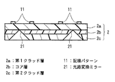
図1〜図6は、本発明の光電気混載基板の製造方法の一実施の形態を示している。この光電気混載基板の製造方法は、図6に示す光電気混載基板を製造する方法である。この光電気混載基板は、図6に示すように、光導波路2の表面に、絶縁層を介さず直接、金属製配線パターン11を形成したものである。
1 to 6 show an embodiment of a method for manufacturing an opto-electric hybrid board according to the present invention. This opto-electric hybrid board manufacturing method is a method of manufacturing the opto-electric hybrid board shown in FIG. As shown in FIG. 6, this opto-electric hybrid board is obtained by forming a
より詳しく説明すると、上記光導波路2は、第1クラッド層2aと第2クラッド層2cとでコア層2bを挟持するとともに被包し、そのコア層2bの所定位置(図6では、左右両側部分)を光路変換ミラー21に形成してなるものとなっている。この光路変換ミラー21は、コア層2bを光軸に対して傾斜した傾斜面に形成した部分であり、その傾斜角度は、光路を変換させる角度によって決まり、通常、光軸に対して45°に設定され、光路を90°変換するように形成される。そして、金属製配線パターン11は、光導波路2の第1クラッド層2aの表面に形成されている。
More specifically, the
このような光電気混載基板は、つぎのようにして製造することができる。 Such an opto-electric hybrid board can be manufactured as follows.
まず、図1に示す、金属薄膜1aが剥離基材1bの表面(図1では下面)に形成された金属薄膜転写シート1を準備し、さらに、下記に説明する、上記第1クラッド層2aおよび第2クラッド層2cの形成材料、ならびにコア層2bの形成材料を準備する。
First, a metal thin
すなわち、上記金属薄膜転写シート1は、通常、市販品を用いるが、作製(例えば、剥離基材1bの表面に、スパッタリング法により金属薄膜1aを形成する等)してもよい。そして、上記金属薄膜1aは、後に配線パターン11(図4参照)に形成されるものであり、その材料は、特に限定されないが、通常、銅が用いられる。金属薄膜1aの厚みも、特に限定されないが、後に形成されるコア層2bと金属薄膜1aの表面(上面)と間の距離を短くする観点から、1.0〜5.0μmの範囲内にすることが好ましい。この距離が1.0μmを下回ると、後に形成される配線パターン11(図4参照)が断線し易くなり、上記距離が5.0μmを上回ると、光信号Lの伝搬効率が不充分になるからである。また、上記剥離基材1bは、上記金属薄膜1aとの接触面に剥離処理が施されており、金属薄膜1aとの剥離が容易になっている。剥離基材1bとしては、特に限定されないが、通常、樹脂シートまたは金属シート等が用いられる。剥離基材1bの厚みも、特に限定されないが、できる限り薄い範囲で、金属薄膜転写シート1の取り扱い性がよくなる程度に剛性が得られる観点から、10〜50μmの範囲内にすることが好ましい。
That is, although the said metal thin
上記第1クラッド層2aおよび第2クラッド層2cの形成材料としては、例えば、エポキシ樹脂が用いられる。また、それ以外の形成材料としては、ポリイミド樹脂前駆体等があげられる。なお、第1クラッド層2aの形成材料と第2クラッド層2cの形成材料とは、同じであってもよいし、異なっていてもよい。
As a material for forming the
上記コア層2bの形成材料としては、例えば、感光性エポキシ樹脂があげられる。また、それ以外の形成材料としては、感光性ポリイミド前駆体等があげられる。
Examples of the material for forming the
なお、光導波路2を構成する関係から、コア層2bは第1クラッド層2aおよび第2クラッド層2cよりも屈折率が高い必要があるが、この屈折率の調整は、例えば、エポキシ樹脂の種類の選択や組成比率を調整して行うことができる。具体的には、コア層2bの屈折率と第1クラッド層2aおよび第2クラッド層2cの屈折率との関係、すなわち、両者の比屈折率差Δ〔比屈折率差Δ=(nコア−nクラッド)/nコア:n=屈折率〕は、通常、0.1〜5.0%の範囲であればよい。
In addition, from the relationship which comprises the
そして、このようにして準備された上記金属薄膜転写シート1および各種形成材料を用いて、つぎのようにして、光電気混載基板を製造する。
Then, using the metal thin
すなわち、図2に示すように、上記金属薄膜転写シート1の金属薄膜1aの表面(図2では下面)に、第1クラッド層2aの形成材料であるエポキシ樹脂ワニス等を、乾燥後の膜厚が好ましくは1〜30μm、特に好ましくは5〜20μmとなるよう塗布し、乾燥させることにより、エポキシ樹脂からなる樹脂層を形成する。上記塗布方法としては、スピンコート法やキャスティング法等の一般的な成膜方法を用いることができる。ついで、UV硬化、加熱することにより上記樹脂層中の残存溶媒の除去および硬化反応を完結させることにより、上記金属薄膜転写シート1の金属薄膜1aの表面にエポキシ樹脂製の第1クラッド層2aを形成する。なお、通常は、図2に図示したものを上下逆さまにした状態で、第1クラッド層2aが形成される。
That is, as shown in FIG. 2, an epoxy resin varnish or the like, which is a material for forming the
つぎに、図3に示すように、上記金属薄膜転写シート1の剥離基材1bを金属薄膜1aから剥離し、その剥離により露呈した金属薄膜1aの表面(第1クラッド層2aとは反対側の表面)に、フォトレジストを用いて、金属製配線パターンと同じパターンのエッチング用レジスト3を形成する。
Next, as shown in FIG. 3, the peeling
ついで、図4に示すように、エッチング液を用いて、エッチング用レジスト3以外の部分の(エッチング用レジスト3から露出している)金属薄膜1aを溶解し除去する。その後、エッチング用レジスト3を除去する。これにより、所定パターンの金属製配線パターン11を形成する。
Next, as shown in FIG. 4, the metal thin film 1 a (exposed from the etching resist 3) other than the etching resist 3 is dissolved and removed using an etching solution. Thereafter, the etching resist 3 is removed. Thereby, the
つぎに、図5に示すように、上記第1クラッド層2aの表面(図5では下面)に、コア層2bの形成材料である感光性エポキシ樹脂ワニス等を、乾燥後の膜厚が好ましくは2〜60μm、特に好ましくは6〜50μmとなるよう塗布し、初期乾燥によりコア層2bとなる感光性エポキシ樹脂層を形成する。ついで、所望のパターンが得られるよう、感光性ポリイミド樹脂前駆体層上にフォトマスクを載置してその上方から紫外線を照射する。この紫外線の照射における露光量は1000〜10000mJ/cm2 である。その後、光反応を完結させるために、Post Exposure Bake(PEB)と呼ばれる露光後の熱処理を行い、現像液を用いて現像を行う(ウェットプロセス法)。そして、現像によって得られた所望のパターンをイミド化するために、通常熱処理を行う。この際の加熱温度は、一般的に100〜150℃である。このようにして硬化することにより、ポリイミド樹脂製のパターンとなるコア層2bを形成する。
Next, as shown in FIG. 5, a photosensitive epoxy resin varnish, which is a material for forming the
その後、コア層2bの表面(下面および側面)を覆うように、第2クラッド層2cを、上記第1クラッド層2aの形成と同様にして形成する。なお、通常は、図5に図示したものを上下逆さまにした状態で、コア層2bおよび第2クラッド層2cが形成される。
Thereafter, the
そして、図6に示すように、レーザ加工,ダイヤモンドブレードを用いたダイシング等により、コア層2bの所定位置(図6では、左右両側部分)を、上記第2クラッド層2cの側から、光軸に対して傾斜した光路変換ミラー(傾斜面)21に形成する。この実施の形態では、コア層2bと第2クラッド層2cとからなる積層部分を断面三角形に切削し、その断面三角形の斜面の一部を上記光路変換ミラー21としている。また、左右の上記光路変換ミラー21の形成位置は、後で説明する発光素子Aおよび受光素子B(図7参照)の下方位置である。このようにして、上記光電気混載基板が製造される。なお、通常は、図6に図示したものを上下逆さまにした状態で、光路変換ミラー21が形成される。
Then, as shown in FIG. 6, the predetermined position of the
このようにして製造された上記光電気混載基板には、図7に示すように、光路変換ミラー21の上方位置に形成されている金属製配線パターン11に、発光素子Aおよび受光素子Bが接続される。
As shown in FIG. 7, the light-emitting element A and the light-receiving element B are connected to the
そして、上記光電気混載基板による光路変換は、つぎのようにして行われる。すなわち、発光素子Aから下方に発せられた光信号Lは、上記光電気混載基板の第1クラッド層2aの表面から入射し、第1クラッド層2a内を透過した後、コア層2bの一方(図7では左側)の光路変換ミラー21で反射し(光路を90°変換し)、コア層2b内に導かれ、再度、他方(図7では右側)の光路変換ミラー21で反射し(光路を90°変換し)、上方の受光素子Bに伝達される。
The optical path conversion by the opto-electric hybrid board is performed as follows. That is, the optical signal L emitted downward from the light emitting element A is incident from the surface of the
この光路変換では、図9に示す従来の光電気混載基板による光路変換と比較すると、金属製配線パターン11形成用の基板50がないため、コア層2bと受光素子Bとの間の距離が短く、光信号Lの伝搬効率が向上している。さらに、この実施の形態では、発光素子Aとコア層2bとの間の距離も短くなっており、光信号Lの伝搬効率がより向上している。
In this optical path conversion, the distance between the
なお、上記実施の形態では、発光素子Aも、光導波路2の表面に形成した金属製配線パターン11に接続させたが、図8に示すように、発光素子Aを、コア層2bの光軸上でその一端面(図8では左端面)の外側近傍に配置し、コア層2bの一方(図7では左側)の光路変換ミラー21を形成しないようにしてもよい。
In the above embodiment, the light emitting element A is also connected to the
また、上記実施の形態では、金属薄膜転写シート1の金属薄膜1aの表面に第1クラッド層2aを形成した後に、金属薄膜転写シート1の剥離基材1bを金属薄膜1aから剥離し、エッチング用レジスト3の形成を経て金属製配線パターン11を形成したが、上記剥離基材1bを剥離する順序は、これに限定されるものではなく、コア層2bを形成した後でもよいし、第2クラッド層2cを形成した後でもよいし、光路変換ミラー21を形成した後でもよい。そして、いずれの場合でも、上記剥離基材1bを剥離した後は、上記実施の形態と同様に、エッチング用レジスト3の形成を経て金属製配線パターン11を形成する。
Moreover, in the said embodiment, after forming the 1st clad
つぎに、実施例について比較例および従来例と併せて説明する。 Next, examples will be described together with comparative examples and conventional examples.
〔金属薄膜転写シート〕
市販の金属薄膜転写シート〔三井金属社製、MicoThin MTSD−H(3μm)〕を準備した。この金属薄膜転写シートは、厚み3μmの銅薄膜が、厚み25μmの剥離基材(銅箔)の表面に形成されているものである。
[Metal thin film transfer sheet]
A commercially available metal thin film transfer sheet [MicoThin MTSD-H (3 μm), manufactured by Mitsui Kinzoku Co., Ltd.] was prepared. In this metal thin film transfer sheet, a copper thin film having a thickness of 3 μm is formed on the surface of a peeling substrate (copper foil) having a thickness of 25 μm.
〔第1クラッド層および第2クラッド層の形成材料〕
BPEFG(長瀬産業社販売、オンコートEX−1020)20g、セロキサイド2021P(ダイセル化学社製)4.1g、SP−170(旭電化社製)0.24gを、シクロへキサン8.47gに溶解することにより、第1クラッド層および第2クラッド層の形成材料である樹脂溶液を得た。
[Formation materials of the first cladding layer and the second cladding layer]
20 g of BPEFG (sold by Nagase Sangyo Co., Ltd., ONCOAT EX-1020), 4.1 g of Celoxide 2021P (manufactured by Daicel Chemical Industries), and 0.24 g of SP-170 (manufactured by Asahi Denka) are dissolved in 8.47 g of cyclohexane. As a result, a resin solution as a material for forming the first cladding layer and the second cladding layer was obtained.
〔コア層の形成材料〕
BPEFG(長瀬産業社販売、オンコートEX−1020)20g、BPFG(長瀬産業社販売、オンコートEX−1010)10g、SP−170(旭電化社製)0.3gを、シクロへキサン20gに溶解することにより、コア層の形成材料である樹脂溶液を得た。
[Material for forming the core layer]
Dissolve 20 g of BPEFG (sold by Nagase Sangyo Co., Ltd., on coat EX-1020), 10 g of BPFG (sold by Nagase Sangyo Co., Ltd., on coat EX-1010), 0.3 g of SP-170 (manufactured by Asahi Denka) in 20 g of cyclohexane. As a result, a resin solution as a material for forming the core layer was obtained.
〔光電気混載基板の製造〕
上記実施の形態(図1〜図6参照)と同様にして、光電気混載基板を製造した。このとき、第1クラッド層および第2クラッド層の厚みをそれぞれ20μmとし、コア層を直線状のパターンに形成し、その寸法を、厚み50μm,幅50μm,長さ5cmとした。また、光路変換ミラーは、レーザ加工により、光軸に対して45°傾斜した傾斜面に形成した。なお、金属製配線パターンを形成する際に用いるエッチング液として、5%NaHCO3 水溶液を用いた。
[Manufacture of opto-electric hybrid board]
An opto-electric hybrid board was manufactured in the same manner as in the above embodiment (see FIGS. 1 to 6). At this time, the thickness of each of the first cladding layer and the second cladding layer was 20 μm, the core layer was formed in a linear pattern, and the dimensions were 50 μm thickness, 50 μm width, and 5 cm length. The optical path conversion mirror was formed on an inclined surface inclined by 45 ° with respect to the optical axis by laser processing. Incidentally, as the etching solution used in forming the metal wiring pattern, with 5% NaHCO 3 aq.
上記実施例1において、金属薄膜転写シートとして、銅薄膜の厚みが5μmのもの〔三井金属社製、MicoThin MTSD−H(3μm)〕を用いた。それ以外は、実施例1と同様にした。 In Example 1 above, a metal thin film transfer sheet having a copper thin film thickness of 5 μm [MicoThin MTSD-H (3 μm), manufactured by Mitsui Kinzoku Co., Ltd.] was used. Otherwise, the same procedure as in Example 1 was performed.
〔製造方法の比較例1〕
上記実施例1において、金属薄膜転写シートに代えて、圧延銅箔(厚み18μm)を用いた。それ以外は、実施例1と同様にした。すなわち、上記圧延銅箔の片面に第1クラッド層を形成した後、圧延銅箔をエッチングすることにより、所定パターンの金属製配線パターンを形成した。そして、上記第1クラッド層の表面にコア層および第2クラッド層を形成した後、光路変換ミラーを形成した。
[Comparative Example 1 of Manufacturing Method]
In Example 1 described above, a rolled copper foil (thickness: 18 μm) was used instead of the metal thin film transfer sheet. Otherwise, the same procedure as in Example 1 was performed. That is, after forming the first cladding layer on one side of the rolled copper foil, the rolled copper foil was etched to form a predetermined metal wiring pattern. Then, after forming the core layer and the second cladding layer on the surface of the first cladding layer, an optical path conversion mirror was formed.
〔従来例1〕
図9に示す従来の光電気混載基板を準備した。この光電気混載基板において、金属製配線パターンが形成された基板の厚みは143μm、金属製配線パターンの厚みは18μmだった。また、光導波路を構成する第1クラッド層,第2クラッド層およびコア層の厚みはそれぞれ実施例1と同様であった。また、基板と光導波路との間の接着剤層の厚みは10μmだった。
[Conventional example 1]
A conventional opto-electric hybrid board shown in FIG. 9 was prepared. In this opto-electric hybrid board, the thickness of the board on which the metal wiring pattern was formed was 143 μm, and the thickness of the metal wiring pattern was 18 μm. The thicknesses of the first cladding layer, the second cladding layer, and the core layer constituting the optical waveguide were the same as those in Example 1. The thickness of the adhesive layer between the substrate and the optical waveguide was 10 μm.
〔光伝搬損失の測定〕
このようにして得られた実施例1,2ならびに比較例1および従来例1の光電気混載基板に、発光素子および受光素子を実装し、光信号を、発光素子から発し、コア層を経て、受光素子に伝達させた。そして、そのときの光伝搬損失を測定した。その結果、実施例1の光伝搬損失は3.0dB、実施例2のそれは3.4dB、比較例1のそれは8.2dB、従来例1のそれは9.5dBであった。
(Measurement of optical propagation loss)
A light emitting element and a light receiving element are mounted on the opto-electric hybrid boards of Examples 1 and 2 and Comparative Example 1 and Conventional Example 1 obtained in this way, and an optical signal is emitted from the light emitting element, through the core layer, It was transmitted to the light receiving element. And the optical propagation loss at that time was measured. As a result, the optical propagation loss of Example 1 was 3.0 dB, that of Example 2 was 3.4 dB, that of Comparative Example 1 was 8.2 dB, and that of Conventional Example 1 was 9.5 dB.
このように、実施例1,2および比較例1の光電気混載基板は、従来例1の光電気混載基板よりも、光伝搬損失が小さいことから、光信号の伝搬効率が高いことがわかる。なかでも、実施例1,2の光電気混載基板は、比較例1の光電気混載基板よりも、光信号の伝搬効率がさらに高いことがわかる。 Thus, it can be seen that the opto-electric hybrid boards of Examples 1 and 2 and Comparative Example 1 have higher optical signal propagation efficiency because the optical propagation loss is smaller than that of the opto-electric hybrid board of Conventional Example 1. In particular, it can be seen that the opto-electric hybrid boards of Examples 1 and 2 have higher optical signal propagation efficiency than the opto-electric hybrid board of Comparative Example 1.
2a 第1クラッド層
2b コア層
2c 第2クラッド層
11 配線パターン
21 光路変換ミラー
2a
Claims (4)
Priority Applications (1)
| Application Number | Priority Date | Filing Date | Title |
|---|---|---|---|
| JP2005296571A JP2007108228A (en) | 2005-10-11 | 2005-10-11 | Photoelectric consolidated substrate and its manufacturing method |
Applications Claiming Priority (1)
| Application Number | Priority Date | Filing Date | Title |
|---|---|---|---|
| JP2005296571A JP2007108228A (en) | 2005-10-11 | 2005-10-11 | Photoelectric consolidated substrate and its manufacturing method |
Publications (1)
| Publication Number | Publication Date |
|---|---|
| JP2007108228A true JP2007108228A (en) | 2007-04-26 |
Family
ID=38034157
Family Applications (1)
| Application Number | Title | Priority Date | Filing Date |
|---|---|---|---|
| JP2005296571A Pending JP2007108228A (en) | 2005-10-11 | 2005-10-11 | Photoelectric consolidated substrate and its manufacturing method |
Country Status (1)
| Country | Link |
|---|---|
| JP (1) | JP2007108228A (en) |
Cited By (4)
| Publication number | Priority date | Publication date | Assignee | Title |
|---|---|---|---|---|
| WO2008136285A1 (en) * | 2007-04-27 | 2008-11-13 | Hitachi Chemical Company, Ltd. | Method for producing photoelectric composite substrate, photoelectric composite substrate produced by the method, and photoelectric composite module using the substrate |
| JP2009058923A (en) * | 2007-04-27 | 2009-03-19 | Hitachi Chem Co Ltd | Method for producing photoelectric composite substrate, photoelectric composite substrate produced by the method, and photoelectric composite module using the same |
| JP2010156801A (en) * | 2008-12-26 | 2010-07-15 | Fuji Xerox Co Ltd | Method for manufacturing polymer optical waveguide |
| US9411112B2 (en) | 2014-07-31 | 2016-08-09 | Fujitsu Limited | Photoelectric hybrid board, information processor, and method for manufacturing photoelectric hybrid board |
Citations (7)
| Publication number | Priority date | Publication date | Assignee | Title |
|---|---|---|---|---|
| JP2001166165A (en) * | 1999-12-08 | 2001-06-22 | Hitachi Cable Ltd | Waveguide film with adhesive sheet and method for packaging the same |
| JP2001525127A (en) * | 1997-05-14 | 2001-12-04 | アライドシグナル・インコーポレーテッド | Ultra-thin conductive layer for printed wiring boards |
| WO2004089049A1 (en) * | 2003-03-28 | 2004-10-14 | Tdk Corporation | Multilayer substrate and method for producing same |
| JP2004341454A (en) * | 2002-05-28 | 2004-12-02 | Matsushita Electric Works Ltd | Manufacturing method of optical circuit-electric circuit consolidation substrate |
| JP2005260058A (en) * | 2004-03-12 | 2005-09-22 | Furukawa Circuit Foil Kk | Carrier-attached very thin copper foil, manufacturing method of carrier-attached very thin copper foil, and wiring board |
| JP2005300930A (en) * | 2004-04-12 | 2005-10-27 | Matsushita Electric Works Ltd | Method for manufacturing optical and electrical consolidated substrate |
| JP2007084765A (en) * | 2005-09-26 | 2007-04-05 | Matsushita Electric Works Ltd | Curable epoxy resin film, optical waveguide using the same and photoelectric composite substrate |
-
2005
- 2005-10-11 JP JP2005296571A patent/JP2007108228A/en active Pending
Patent Citations (7)
| Publication number | Priority date | Publication date | Assignee | Title |
|---|---|---|---|---|
| JP2001525127A (en) * | 1997-05-14 | 2001-12-04 | アライドシグナル・インコーポレーテッド | Ultra-thin conductive layer for printed wiring boards |
| JP2001166165A (en) * | 1999-12-08 | 2001-06-22 | Hitachi Cable Ltd | Waveguide film with adhesive sheet and method for packaging the same |
| JP2004341454A (en) * | 2002-05-28 | 2004-12-02 | Matsushita Electric Works Ltd | Manufacturing method of optical circuit-electric circuit consolidation substrate |
| WO2004089049A1 (en) * | 2003-03-28 | 2004-10-14 | Tdk Corporation | Multilayer substrate and method for producing same |
| JP2005260058A (en) * | 2004-03-12 | 2005-09-22 | Furukawa Circuit Foil Kk | Carrier-attached very thin copper foil, manufacturing method of carrier-attached very thin copper foil, and wiring board |
| JP2005300930A (en) * | 2004-04-12 | 2005-10-27 | Matsushita Electric Works Ltd | Method for manufacturing optical and electrical consolidated substrate |
| JP2007084765A (en) * | 2005-09-26 | 2007-04-05 | Matsushita Electric Works Ltd | Curable epoxy resin film, optical waveguide using the same and photoelectric composite substrate |
Cited By (6)
| Publication number | Priority date | Publication date | Assignee | Title |
|---|---|---|---|---|
| WO2008136285A1 (en) * | 2007-04-27 | 2008-11-13 | Hitachi Chemical Company, Ltd. | Method for producing photoelectric composite substrate, photoelectric composite substrate produced by the method, and photoelectric composite module using the substrate |
| JP2009058923A (en) * | 2007-04-27 | 2009-03-19 | Hitachi Chem Co Ltd | Method for producing photoelectric composite substrate, photoelectric composite substrate produced by the method, and photoelectric composite module using the same |
| US8244080B2 (en) | 2007-04-27 | 2012-08-14 | Hitachi Chemical Company, Ltd. | Method for producing photoelectric composite substrate, photoelectric composite substrate produced by the method, and photoelectric composite module using the substrate |
| TWI456274B (en) * | 2007-04-27 | 2014-10-11 | Hitachi Chemical Co Ltd | Manufacturing method of an optoelectronic composite substrate, optoelectronic composite substrate manufactured by said manufacturing method, and optoelectronic composite module using said optoelectronic composite substrate |
| JP2010156801A (en) * | 2008-12-26 | 2010-07-15 | Fuji Xerox Co Ltd | Method for manufacturing polymer optical waveguide |
| US9411112B2 (en) | 2014-07-31 | 2016-08-09 | Fujitsu Limited | Photoelectric hybrid board, information processor, and method for manufacturing photoelectric hybrid board |
Similar Documents
| Publication | Publication Date | Title |
|---|---|---|
| JP4714195B2 (en) | Optical printed circuit board manufacturing method | |
| CN102369467B (en) | Manufacture the method for optical waveguide core, the method manufacturing optical waveguide, optical waveguide and optoelectronic composite wiring board | |
| KR100976671B1 (en) | Process for producing optical waveguide | |
| JP4153007B2 (en) | Optical wiring board and opto-electric hybrid board | |
| WO2004027472A1 (en) | Optical waveguide and method for manufacturing same | |
| JP2009175418A (en) | Opto-electronic printed wiring board and manufacturing method of same | |
| JP2005275405A (en) | Optical structure and method for connecting optical circuit board components | |
| TW201142391A (en) | Optical waveguide substrate having positioning structure, method for manufacturing same, and method for manufacturing opto-electric hybrid substrate | |
| JP2007148087A (en) | Optoelectrical integrated wiring board and optoelectrical integrated wiring system | |
| JP2011113039A (en) | Optical waveguide device and method of manufacturing the same | |
| US7106921B2 (en) | Optical waveguide interconnection board, method of manufacturing the same, precursor for use in manufacturing optical waveguide interconnection board, and photoelectric multifunction board | |
| JP2001007463A (en) | Substrate for mixedly mounting optical and electrical parts and its manufacture | |
| JP2005195651A (en) | Optical connection substrate, optical transmission system, and manufacturing method | |
| JP2006156439A (en) | Manufacturing method of photoelectricity mixed loading substrate | |
| JP2007108228A (en) | Photoelectric consolidated substrate and its manufacturing method | |
| JP2014077825A (en) | Manufacturing method of optical interconnect device and optical interconnect device | |
| KR100813919B1 (en) | optical connection block for PCB and method for fabrication thereof | |
| JP4441994B2 (en) | Optical wiring layer manufacturing method and optical / electrical wiring board | |
| JP2004163914A (en) | Manufacturing method of optical circuit board | |
| JP4962265B2 (en) | Optical waveguide manufacturing method | |
| JP2005099521A (en) | Optical transmission device | |
| JP4339198B2 (en) | Manufacturing method of optical module | |
| JP4742771B2 (en) | Method for manufacturing photoelectric composite substrate | |
| JP2005128319A (en) | Optical functional element and its manufacturing method | |
| JP6168598B2 (en) | Opto-electric hybrid module |
Legal Events
| Date | Code | Title | Description |
|---|---|---|---|
| A621 | Written request for application examination |
Free format text: JAPANESE INTERMEDIATE CODE: A621 Effective date: 20071113 |
|
| A131 | Notification of reasons for refusal |
Free format text: JAPANESE INTERMEDIATE CODE: A131 Effective date: 20091110 |
|
| A977 | Report on retrieval |
Free format text: JAPANESE INTERMEDIATE CODE: A971007 Effective date: 20091110 |
|
| A02 | Decision of refusal |
Free format text: JAPANESE INTERMEDIATE CODE: A02 Effective date: 20100406 |