JP2007103997A - Electromagnetic wave emission device - Google Patents
Electromagnetic wave emission device Download PDFInfo
- Publication number
- JP2007103997A JP2007103997A JP2005287342A JP2005287342A JP2007103997A JP 2007103997 A JP2007103997 A JP 2007103997A JP 2005287342 A JP2005287342 A JP 2005287342A JP 2005287342 A JP2005287342 A JP 2005287342A JP 2007103997 A JP2007103997 A JP 2007103997A
- Authority
- JP
- Japan
- Prior art keywords
- electromagnetic wave
- optical
- beat signal
- electromagnetic
- optical beat
- Prior art date
- Legal status (The legal status is an assumption and is not a legal conclusion. Google has not performed a legal analysis and makes no representation as to the accuracy of the status listed.)
- Pending
Links
Images

Abstract
Description
本発明は、イメージングや材料分析に用いられるミリ波帯からテラヘルツ波帯の電磁波を発生する電磁波放射装置に関する。 The present invention relates to an electromagnetic wave radiation device that generates an electromagnetic wave of a terahertz wave band from a millimeter wave band used for imaging and material analysis.
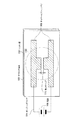
従来の電磁波放射装置として、例えば非特許文献1に開示されたものがある。図5は従来の電磁波放射装置を示す構成図、図6は図5に示す電磁波放射装置のシリコン層の裏面を示す図である。 For example, Non-Patent Document 1 discloses a conventional electromagnetic wave radiation device. FIG. 5 is a block diagram showing a conventional electromagnetic wave emission device, and FIG. 6 is a view showing the back surface of the silicon layer of the electromagnetic wave emission device shown in FIG.
図5に示す電磁波放射装置は、サファイア基板101と、サファイア基板101に張り付けされ、イオン打ち込みされたシリコン層102と、MgOで作られた半球レンズ103と、シリコン層102の裏面のパターンに導通を取るためのボンディングワイヤ104と、フェムト秒パルスレーザ105と、電源106と、フェムト秒パルスレーザ光をコリメートするための光学系107と、テラヘルツ電磁波をコリメートするためのパラボラ型反射ミラー108とを備える。
The electromagnetic wave emission device shown in FIG. 5 is electrically connected to the sapphire substrate 101, the silicon layer 102 which is attached to the sapphire substrate 101 and is ion-implanted, the hemispherical lens 103 made of MgO, and the back surface pattern of the silicon layer 102. It includes a bonding wire 104 for taking, a
また、サファイア基板101の裏面には図6に示すように、イオン打ち込みされたシリコン層102があり、その表面にアルミ配線により微小ギャップ111付きのダイポールアンテナペア109が形成されている。 Further, as shown in FIG. 6, an ion-implanted silicon layer 102 is provided on the back surface of the sapphire substrate 101, and a dipole antenna pair 109 with a minute gap 111 is formed on the front surface by aluminum wiring.
点線で示す円110は、サファイア基板101の表面側に設置された半球レンズ103とダイポールアンテナペア109の微小ギャップ111との位置関係を示す線である。ダイポールアンテナペア109にはボンディングワイヤ104により導通を取り、電源106より電圧を印加する。
A
フェムト秒パルスレーザ105から発生したフェムト秒パルス光は、コリメート光学系107によりダイポールアンテナペア109の微小ギャップ111に照射される。光照射でシリコン層102に発生したキャリアは印加電界により移動するため、ダイポールアンテナペア109に変位電流を発生させる。この変位電流は、立ち上がりが照射されるフェムト秒レーザのパルス幅に一致し、テラヘルツ帯の周波数成分を含んでいる。
The femtosecond pulse light generated from the
したがって、ダイポールアンテナペア109はテラヘルツ波放射器として機能し、サファイア基板101の方向にテラヘルツ波を照射する。サファイア基板101を通過したテラヘルツ波は半球レンズ103で放射角θが狭められ、パラボラ型反射ミラー108方向に放射される。そしてパラボラ型反射ミラー108で放射方向が90度曲げられ、かつ平行ビームにコリメートされる。
図5に示す電磁波放射装置では、コリメートしたテラヘルツビームの方向を変えるためには、以下の(1),(2)のいずれかを行う必要がある。 In the electromagnetic wave emission device shown in FIG. 5, in order to change the direction of the collimated terahertz beam, one of the following (1) and (2) must be performed.
(1)コリメート光学系107からパラボラ型反射ミラー108までを一体化して可動ステージに搭載し、これを動かす。 (1) The collimating optical system 107 to the parabolic reflection mirror 108 are integrated and mounted on a movable stage, and this is moved.
(2)出力ビームを平行に保ちながらビームがステアリングできるような複雑な動きを可能とする角度調整機能をパラボラ型反射ミラー108に持たせる。 (2) The parabolic reflection mirror 108 is provided with an angle adjustment function that enables a complicated movement that allows the beam to be steered while keeping the output beam parallel.
しかし、いずれも複雑な光学系を組む必要があるという問題があった。 However, there is a problem that all of them require a complicated optical system.
本発明は上記に鑑みてなされたもので、簡素な構造で、電磁波を所望の方向に向けて放射できる電磁波放射装置を提供することを目的とする。 The present invention has been made in view of the above, and an object thereof is to provide an electromagnetic wave radiation device capable of radiating an electromagnetic wave in a desired direction with a simple structure.
上記目的を達成するため、請求項1記載の発明は、ミリ波帯からテラヘルツ波帯の範囲の波長帯域の電磁波のうちで少なくとも1つの波長の電磁波を放射する電磁波放射装置において、光ビート信号を発生する光ビート信号発生手段と、前記光ビート信号をnチャンネルに分岐する光分岐手段と、この光分岐手段により分岐されるnチャンネルの前記光ビート信号の遅延量をそれぞれ独立に調整して出力する光遅延手段と、この光遅延手段からの前記光ビート信号を受けて電磁波を放射する電磁波放射素子がアレイ状にn素子配置された電磁波放射源と、前記光遅延手段から出力されるnチャンネルの前記光ビート信号の遅延量を制御することにより前記電磁波放射素子が放射する電磁波の位相をそれぞれ制御し、これにより前記電磁波放射源が放射する電磁波の方向を制御する制御手段とを備えたことを特徴とする。 In order to achieve the above object, an invention according to claim 1 is an electromagnetic wave emission device for emitting an electromagnetic wave having at least one wavelength among electromagnetic waves in a wavelength band ranging from a millimeter wave band to a terahertz wave band. An optical beat signal generating means for generating, an optical branching means for branching the optical beat signal into n channels, and a delay amount of the optical beat signal of the n channel branched by the optical branching means are independently adjusted and output. An optical delay means for receiving the optical beat signal from the optical delay means, an electromagnetic wave radiation source for radiating electromagnetic waves in an array, and an n-channel output from the optical delay means By controlling the delay amount of the optical beat signal, the phase of the electromagnetic wave radiated by the electromagnetic wave radiating element is respectively controlled. There is characterized in that a control means for controlling the direction of the electromagnetic wave radiation.
請求項2記載の発明は、前記電磁波放射素子は、前記光ビート信号を受けて高周波電流を発生する光電変換手段と、この光電変換手段で発生した高周波電流に応じた電磁波を2次的に空中に放射する平面アンテナとを備えたことを特徴とする。 According to a second aspect of the present invention, the electromagnetic wave radiating element includes a photoelectric conversion unit that generates a high-frequency current in response to the optical beat signal, and a second electromagnetic wave corresponding to the high-frequency current generated by the photoelectric conversion unit. And a planar antenna for radiating the light.
請求項3記載の発明は、前記平面アンテナは、前記光電変換手段に照射される前記光ビート信号の進行方向と同一方向に電磁波を放射することを特徴とする。 The invention according to claim 3 is characterized in that the planar antenna radiates an electromagnetic wave in the same direction as the traveling direction of the optical beat signal applied to the photoelectric conversion means.
請求項4記載の発明は、ミリ波帯からテラヘルツ波帯の範囲の波長帯域の電磁波のうちで少なくとも1つの波長の電磁波を放射する電磁波放射装置において、電磁波を放射する電磁波放射素子をアレイ状に配置した電磁波放射源と、前記複数の電磁波放射素子が放射する電磁波の位相をそれぞれ制御することにより前記電磁波放射源が放射する電磁波の方向を制御する制御手段とを備えたことを特徴とする。 According to a fourth aspect of the present invention, there is provided an electromagnetic wave radiation device that radiates an electromagnetic wave having at least one wavelength among electromagnetic waves in a wavelength band ranging from a millimeter wave band to a terahertz wave band. An electromagnetic wave radiation source arranged, and a control means for controlling the direction of the electromagnetic wave emitted from the electromagnetic wave radiation source by respectively controlling the phase of the electromagnetic wave emitted from the plurality of electromagnetic wave radiation elements.
本発明によれば、電磁波を放射する複数の電磁波放射素子をアレイ状に配置し、それぞれの電磁波放射素子が放射する電磁波の位相を調整することにより電磁波放射源が放射する電磁波の方向を制御するので、簡素な構造で、電磁波を所望の方向に向けて放射できる電磁波放射装置を提供することができる。 According to the present invention, a plurality of electromagnetic wave radiating elements that radiate electromagnetic waves are arranged in an array, and the direction of the electromagnetic waves radiated from the electromagnetic wave radiation source is controlled by adjusting the phase of the electromagnetic waves radiated by the respective electromagnetic wave radiating elements. Therefore, it is possible to provide an electromagnetic wave radiation device that can radiate an electromagnetic wave in a desired direction with a simple structure.
以下、本発明の電磁波放射装置を実施するための最良の形態について、図面を参照して説明する。図1は本発明の実施の形態の電磁波放射装置を示す構成図である。 The best mode for carrying out the electromagnetic wave emission device of the present invention will be described below with reference to the drawings. FIG. 1 is a block diagram showing an electromagnetic wave radiation device according to an embodiment of the present invention.
図1に示すように本実施の形態の電磁波放射装置は、光電変換によりテラヘルツ波が発生するような光ビート信号を発生する光ビート信号発生部1と、光ビート信号発生部1から入力される光ビート信号をnチャンネルに分岐する光分岐部2と、n個の移相器31〜3nを有し、光分岐部2から入力されるnチャンネルの光ビート信号の遅延量をそれぞれ独立に調整する光遅延回路3と、nチャンネルの2次元光ファイバアレイ4と、2次元光ファイバアレイ4から出射されるnチャンネルの光ビート信号をコリメートするコリメートレンズ5と、アレイ状にテラヘルツ波放射素子がn素子配置されたテラヘルツ波放射源6と、中央に穴があり裏面からの光がテラヘルツ波放射源6に照射されるようになっている放射源マウンタ7と、テラヘルツ波放射源6のn個のテラヘルツ波放射素子にバイアス電圧を印加するための電源8と、光遅延回路3を制御しテラヘルツ波放射源6から放射されるテラヘルツ波の方向を制御する制御部9とを備える。なお、以下ではn=9とする。
As shown in FIG. 1, the electromagnetic wave emission device according to the present embodiment is input from an optical beat signal generator 1 that generates an optical beat signal that generates a terahertz wave by photoelectric conversion, and an optical beat signal generator 1. It has an
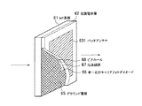
図2は図1に示す電磁波放射装置のテラヘルツ波放射源を示す構成図である。図2に示すようにテラヘルツ波放射源6は、InP基板61と、InP基板61上に形成された低誘電体層62と、低誘電体層62上にパッチアンテナ631〜639を3行×3列に並べて形成されたパッチアンテナアレイ63と、低誘電体層62の下層に存在する給電素子へ直流電圧を供給する電極パッド64とを備える。 FIG. 2 is a block diagram showing a terahertz wave radiation source of the electromagnetic wave radiation device shown in FIG. As shown in FIG. 2, the terahertz radiation source 6 includes an InP substrate 61, a low dielectric layer 62 formed on the InP substrate 61, and patch antennas 631 to 639 on the low dielectric layer 62 in 3 rows × 3. A patch antenna array 63 formed side by side and an electrode pad 64 for supplying a DC voltage to a power feeding element existing below the low dielectric layer 62 are provided.
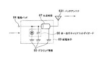
図3はパッチアンテナの下層にある給電素子を示す図、図4は給電素子の回路図である。パッチアンテナ631〜639の給電素子はすべて同様の構成であるので、パッチアンテナ631の給電素子を例に図示している。図3及び図4に示すように給電素子69は、InP基板61上に形成されたグラウンド電極65と、InP基板61上に形成され、光ビート信号を受けて相応の周波数で振動する高周波電流を発生する裏面光入射型の単一走行キャリアフォトダイオード66と、単一走行キャリアフォトダイオード66で発生した高周波電流を伝える伝送線路67と、伝送線路67を伝わってきた高周波電流を低誘電体層62を貫通させてパッチアンテナ631に伝えるビアホール68とを備える。 FIG. 3 is a diagram showing a feed element under the patch antenna, and FIG. 4 is a circuit diagram of the feed element. Since all the feeding elements of the patch antennas 631 to 639 have the same configuration, the feeding element of the patch antenna 631 is illustrated as an example. As shown in FIGS. 3 and 4, the power feeding element 69 includes a ground electrode 65 formed on the InP substrate 61 and a high-frequency current that is formed on the InP substrate 61 and oscillates at an appropriate frequency in response to the optical beat signal. The backside light incident type single traveling carrier photodiode 66 that is generated, the transmission line 67 that transmits the high-frequency current generated by the single traveling carrier photodiode 66, and the high-frequency current that has been transmitted through the transmission line 67 are reduced to the low dielectric layer 62. And a via hole 68 that is transmitted to the patch antenna 631.
この構造は、半絶縁性InP基板61上にエピタキシャル成長させた化合物半導体ヘテロ接合構造に対して、通常のフォトリソグラフィ、エッチング、メタルリフトオフなどを施すことで作製可能である。一例として、パッチアンテナ631を240ミクロン×240ミクロンとすれば、パッチアンテナ631は300GHz付近に共振周波数を持つ。 This structure can be produced by subjecting a compound semiconductor heterojunction structure epitaxially grown on the semi-insulating InP substrate 61 to normal photolithography, etching, metal lift-off, and the like. As an example, if the patch antenna 631 is 240 microns × 240 microns, the patch antenna 631 has a resonance frequency near 300 GHz.
ここで、本実施の形態の電磁波放射装置の動作を説明する。まず、光ビート信号発生部1は、光電変換によりテラヘルツ波が発生するような光ビート信号を発生し、光分岐部2に出力する。
Here, the operation of the electromagnetic wave emission device of the present exemplary embodiment will be described. First, the optical beat signal generation unit 1 generates an optical beat signal that generates a terahertz wave by photoelectric conversion, and outputs the optical beat signal to the
次いで、光分岐部2は、光ビート信号発生部1から入力された光ビート信号を9チャンネルに分岐し、光遅延回路3の移相器31〜39にそれぞれ出力する。
Next, the
その後、移相器31〜39は、制御部9からの制御指示に基づいて、光分岐部2から入力された光ビート信号の遅延量をそれぞれ独立に調整した後、3×3の2次元光ファイバアレイ4を経由してコリメートレンズ5に光ビート信号を放射する。
After that, the phase shifters 31 to 39 independently adjust the delay amount of the optical beat signal input from the
そして、コリメートレンズ5は、光ビート信号をコリメートし、テラヘルツ波放射源6に裏面から照射する。ここで、2次元光ファイバアレイ4のそれぞれの光ファイバから出射された光ビート信号は、対角の位置にあるパッチアンテナの給電素子に照射される。 The collimating lens 5 collimates the optical beat signal and irradiates the terahertz wave radiation source 6 from the back surface. Here, the optical beat signals emitted from the respective optical fibers of the two-dimensional optical fiber array 4 are applied to the feeding elements of the patch antenna at diagonal positions.
そして、給電素子69の単一走行キャリアフォトダイオード66は、光ビート信号を受けて相応の周波数で振動する高周波電流を発生する。この高周波電流は伝送線路67、ビアホール68を経由してパッチアンテナ631に伝えられる。そして、パッチアンテナ631は、高周波電流に応じたテラヘルツ波を2次的に空中に放射する。各パッチアンテナ631〜639で同様にテラヘルツ波が放射される。 The single traveling carrier photodiode 66 of the feed element 69 receives the optical beat signal and generates a high-frequency current that vibrates at a corresponding frequency. This high-frequency current is transmitted to the patch antenna 631 via the transmission line 67 and the via hole 68. The patch antenna 631 secondarily radiates a terahertz wave corresponding to the high-frequency current into the air. Similarly, terahertz waves are radiated from the patch antennas 631 to 639.
アレイ状に並べられたパッチアンテナ631〜639からそれぞれ放射されたテラヘルツ波は互いに干渉し合い、特定の方向にのみ強く放射される。そこで、制御部9は、各パッチアンテナ631〜639を励起する位相を制御することによってその干渉波の放射分布を制御し、テラヘルツ波の放射方向を制御する。 The terahertz waves radiated from the patch antennas 631 to 639 arranged in an array interfere with each other and are radiated strongly only in a specific direction. Therefore, the control unit 9 controls the radiation distribution of the interference wave by controlling the phase for exciting the patch antennas 631 to 639, and controls the radiation direction of the terahertz wave.
ここで、制御部9は、9つのパッチアンテナ631〜639から放射されるテラヘルツ波が任意の一方向に絞られて向かうように、移相器31〜39で各チャンネルに与える光遅延量を制御する。 Here, the control unit 9 controls the optical delay amount given to each channel by the phase shifters 31 to 39 so that the terahertz waves radiated from the nine patch antennas 631 to 639 are narrowed in one arbitrary direction. To do.
このように本実施の形態の電磁波放射装置によれば、パッチアンテナ631〜639を励起する各光ビート信号の遅延を制御することにより、パッチアンテナアレイ63から放射されるテラヘルツ波を、放射方向がある特定の方向に定まった収束ビームとして放射させることができるので、テラヘルツ波放射源6を移動させることなく、また可動ミラーなどの複雑な光学系を用いることなくテラヘルツ波を所望の方向に向けて発射できることが可能になる。 As described above, according to the electromagnetic wave radiation device of the present embodiment, the radiation direction of the terahertz wave radiated from the patch antenna array 63 is controlled by controlling the delay of each optical beat signal that excites the patch antennas 631 to 639. Since it can be radiated as a convergent beam defined in a specific direction, the terahertz wave is directed in a desired direction without moving the terahertz wave radiation source 6 and without using a complicated optical system such as a movable mirror. It becomes possible to launch.
また、単一走行キャリアフォトダイオード66と低誘電体層62を挟んで相対する位置に設置されたパッチアンテナ631によりテラヘルツ波を放射するので、単一走行キャリアフォトダイオード66を照射する光ビート信号の進行方向とパッチアンテナ631から放射されるテラヘルツ波の放射方向が同一方向となり、放射テラヘルツ波が、単一走行キャリアフォトダイオード66への光ビート信号集光用のコリメートレンズ5と干渉することがなく、自由に放射テラヘルツ波の出射方向を調整することが可能となる。 In addition, since the terahertz wave is radiated by the patch antenna 631 disposed at a position facing the single traveling carrier photodiode 66 and the low dielectric layer 62, the optical beat signal of the single traveling carrier photodiode 66 is irradiated. The traveling direction and the radiation direction of the terahertz wave radiated from the patch antenna 631 are the same direction, and the radiated terahertz wave does not interfere with the collimating lens 5 for collecting the optical beat signal to the single traveling carrier photodiode 66. It is possible to freely adjust the emission direction of the radiation terahertz wave.
また、パッチアンテナ631〜639をアレイ状に配置したので、アレイ化によるパワー合成で得られるパワーを稼ぐことができる。 Further, since the patch antennas 631 to 639 are arranged in an array, it is possible to earn power obtained by power synthesis by arraying.
なお、光遅延回路3としては、レンズと可動反射プリズムを組み合わせた空間型光遅延回路でも実現可能であるし、ファイバ統合型の光位相変調器を用いても実現できる。 The optical delay circuit 3 can be realized by a spatial optical delay circuit in which a lens and a movable reflecting prism are combined, or by using a fiber integrated optical phase modulator.
また、本実施の形態では、放射する電磁波の周波数は300GHzに限るものではなく、ミリ波帯からテラヘルツ帯の範囲のいずれの周波数の電磁波を用いてもかまわない。また、パッチアンテナアレイ63を形成するアンテナの配列も3行3列に限るものではなく、何行何列でもよい。また、アンテナの形状もパッチアンテナに限るものではなく、ダイポール、ログペリなど他の形状でもよい。 In the present embodiment, the frequency of the radiated electromagnetic wave is not limited to 300 GHz, and an electromagnetic wave having any frequency in the range from the millimeter wave band to the terahertz band may be used. Further, the arrangement of antennas forming the patch antenna array 63 is not limited to 3 rows and 3 columns, and may be any number of rows and columns. Also, the shape of the antenna is not limited to the patch antenna, but may be other shapes such as a dipole or log peri.
1 光ビート信号発生部
2 光分岐部
3 光遅延回路
4 2次元光ファイバアレイ
5 コリメートレンズ
6 テラヘルツ波放射源
7 放射源マウンタ
8 電源
9 制御部
31〜39 移相器
61 InP基板
62 低誘電体層
63 パッチアンテナアレイ
631〜639 パッチアンテナ
64 電極パッド
65 グラウンド電極
66 単一走行キャリアフォトダイオード
67 伝送線路
68 ビアホール
DESCRIPTION OF SYMBOLS 1 Optical beat
Claims (4)
光ビート信号を発生する光ビート信号発生手段と、
前記光ビート信号をnチャンネルに分岐する光分岐手段と、
この光分岐手段により分岐されるnチャンネルの前記光ビート信号の遅延量をそれぞれ独立に調整して出力する光遅延手段と、
この光遅延手段からの前記光ビート信号を受けて電磁波を放射する電磁波放射素子がアレイ状にn素子配置された電磁波放射源と、
前記光遅延手段から出力されるnチャンネルの前記光ビート信号の遅延量を制御することにより前記電磁波放射素子が放射する電磁波の位相をそれぞれ制御し、これにより前記電磁波放射源が放射する電磁波の方向を制御する制御手段と
を備えたことを特徴とする電磁波放射装置。 In an electromagnetic wave emission device that radiates electromagnetic waves of at least one wavelength among electromagnetic waves in a wavelength band ranging from the millimeter wave band to the terahertz wave band,
An optical beat signal generating means for generating an optical beat signal;
Optical branching means for branching the optical beat signal into n channels;
An optical delay means for independently adjusting and outputting delay amounts of the optical beat signals of the n channels branched by the optical branch means;
An electromagnetic wave radiation source in which n elements arranged in an array form receive electromagnetic wave radiation elements that receive the optical beat signal from the optical delay means, and radiate electromagnetic waves;
The phase of the electromagnetic wave emitted by the electromagnetic wave radiation element is controlled by controlling the delay amount of the optical beat signal of the n channel output from the optical delay means, and thereby the direction of the electromagnetic wave emitted by the electromagnetic wave radiation source An electromagnetic wave radiation device comprising: control means for controlling
前記光ビート信号を受けて高周波電流を発生する光電変換手段と、
この光電変換手段で発生した高周波電流に応じた電磁波を2次的に空中に放射する平面アンテナと
を備えたことを特徴とする請求項1に記載の電磁波放射装置。 The electromagnetic radiation element is:
Photoelectric conversion means for receiving the optical beat signal and generating a high-frequency current;
The electromagnetic wave radiation device according to claim 1, further comprising: a planar antenna that secondarily radiates electromagnetic waves according to the high-frequency current generated by the photoelectric conversion means into the air.
電磁波を放射する電磁波放射素子をアレイ状に配置した電磁波放射源と、
前記複数の電磁波放射素子が放射する電磁波の位相をそれぞれ制御することにより前記電磁波放射源が放射する電磁波の方向を制御する制御手段と
を備えたことを特徴とする電磁波放射装置。
In an electromagnetic wave emission device that radiates electromagnetic waves of at least one wavelength among electromagnetic waves in a wavelength band ranging from the millimeter wave band to the terahertz wave band,
An electromagnetic radiation source in which electromagnetic radiation elements that emit electromagnetic waves are arranged in an array; and
An electromagnetic wave radiation device comprising: control means for controlling the direction of the electromagnetic wave emitted by the electromagnetic wave radiation source by controlling the phase of the electromagnetic wave emitted by the plurality of electromagnetic wave radiation elements.
Priority Applications (1)
| Application Number | Priority Date | Filing Date | Title |
|---|---|---|---|
| JP2005287342A JP2007103997A (en) | 2005-09-30 | 2005-09-30 | Electromagnetic wave emission device |
Applications Claiming Priority (1)
| Application Number | Priority Date | Filing Date | Title |
|---|---|---|---|
| JP2005287342A JP2007103997A (en) | 2005-09-30 | 2005-09-30 | Electromagnetic wave emission device |
Publications (1)
| Publication Number | Publication Date |
|---|---|
| JP2007103997A true JP2007103997A (en) | 2007-04-19 |
Family
ID=38030551
Family Applications (1)
| Application Number | Title | Priority Date | Filing Date |
|---|---|---|---|
| JP2005287342A Pending JP2007103997A (en) | 2005-09-30 | 2005-09-30 | Electromagnetic wave emission device |
Country Status (1)
| Country | Link |
|---|---|
| JP (1) | JP2007103997A (en) |
Cited By (5)
| Publication number | Priority date | Publication date | Assignee | Title |
|---|---|---|---|---|
| JP2009210422A (en) * | 2008-03-04 | 2009-09-17 | Sony Corp | Probe device and terahertz spectroscopic apparatus |
| WO2009131113A1 (en) | 2008-04-25 | 2009-10-29 | 独立行政法人理化学研究所 | Terahertz beam steering apparatus and method thereof |
| WO2016208049A1 (en) * | 2015-06-26 | 2016-12-29 | 株式会社日立製作所 | Laser light position control device and measuring device |
| JPWO2021070903A1 (en) * | 2019-10-09 | 2021-04-15 | ||
| WO2024067977A1 (en) * | 2022-09-29 | 2024-04-04 | Nokia Solutions And Networks Oy | Apparatus comprising a plurality of resonant tunneling diode elements, method of manufacturing such apparatus, method of operating such apparatus |
-
2005
- 2005-09-30 JP JP2005287342A patent/JP2007103997A/en active Pending
Cited By (9)
| Publication number | Priority date | Publication date | Assignee | Title |
|---|---|---|---|---|
| JP2009210422A (en) * | 2008-03-04 | 2009-09-17 | Sony Corp | Probe device and terahertz spectroscopic apparatus |
| WO2009131113A1 (en) | 2008-04-25 | 2009-10-29 | 独立行政法人理化学研究所 | Terahertz beam steering apparatus and method thereof |
| JP2009265361A (en) * | 2008-04-25 | 2009-11-12 | Institute Of Physical & Chemical Research | Terahertz beam scanning apparatus and method |
| US8121157B2 (en) | 2008-04-25 | 2012-02-21 | Riken | Terahertz beam scanning apparatus and method thereof |
| WO2016208049A1 (en) * | 2015-06-26 | 2016-12-29 | 株式会社日立製作所 | Laser light position control device and measuring device |
| JPWO2016208049A1 (en) * | 2015-06-26 | 2017-08-17 | 株式会社日立製作所 | Laser light position control device and measuring device |
| JPWO2021070903A1 (en) * | 2019-10-09 | 2021-04-15 | ||
| JP7346584B2 (en) | 2019-10-09 | 2023-09-19 | パイオニア株式会社 | electromagnetic wave generator |
| WO2024067977A1 (en) * | 2022-09-29 | 2024-04-04 | Nokia Solutions And Networks Oy | Apparatus comprising a plurality of resonant tunneling diode elements, method of manufacturing such apparatus, method of operating such apparatus |
Similar Documents
| Publication | Publication Date | Title |
|---|---|---|
| US9557585B1 (en) | Stacked rows pseudo-randomly spaced two-dimensional phased array assembly | |
| US20230236471A1 (en) | Phase front shaping in one and two-dimensional optical phased arrays | |
| JP4858559B2 (en) | Radar equipment | |
| US4929956A (en) | Optical beam former for high frequency antenna arrays | |
| US10739256B1 (en) | Spectroscopy system with beat component | |
| CA2630379C (en) | Frequency scanning antenna | |
| US8934774B2 (en) | Phase shifter and photonic controlled beam former for phased array antennas | |
| US6825814B2 (en) | Antenna | |
| US7884777B2 (en) | Free-space-optically-synchronized wafer scale antenna module osillators | |
| KR20030015214A (en) | Reconfigurable antenna | |
| JP5731745B2 (en) | Antenna device and radar device | |
| JP2007103997A (en) | Electromagnetic wave emission device | |
| KR102257556B1 (en) | Apparatus for generating terahertz wave and method for controlling terahertz wavefront using the same | |
| US20080036669A1 (en) | Coherent near-field array | |
| Ortega et al. | Optical beamformer for 2-D phased array antenna with subarray partitioning capability | |
| JP4563815B2 (en) | Optical and frequency scanning arrays | |
| US10082627B2 (en) | Apparatus and method for providing terahertz waves | |
| JP2021507282A (en) | Laser beam deflector | |
| JP3009631B2 (en) | Optically controlled phased array antenna | |
| AU2006314463B2 (en) | Frequency scanning antenna | |
| JP2508707B2 (en) | Light control antenna device | |
| JP2011128059A (en) | Radio wave target simulation system | |
| JP2021197656A (en) | Lens antenna | |
| JPH11205027A (en) | Antenna system | |
| KR102615794B1 (en) | Reconfigurable metasurface antenna |