JP2007088056A - Wiring circuit board - Google Patents
Wiring circuit board Download PDFInfo
- Publication number
- JP2007088056A JP2007088056A JP2005272498A JP2005272498A JP2007088056A JP 2007088056 A JP2007088056 A JP 2007088056A JP 2005272498 A JP2005272498 A JP 2005272498A JP 2005272498 A JP2005272498 A JP 2005272498A JP 2007088056 A JP2007088056 A JP 2007088056A
- Authority
- JP
- Japan
- Prior art keywords
- ground
- layer
- metal
- insulating layer
- insulating
- Prior art date
- Legal status (The legal status is an assumption and is not a legal conclusion. Google has not performed a legal analysis and makes no representation as to the accuracy of the status listed.)
- Granted
Links
Images


Abstract
Description
本発明は、配線回路基板に関し、詳しくは、高密度化や高速化に対応した配線回路基板に関する。 The present invention relates to a printed circuit board, and more particularly to a printed circuit board that supports high density and high speed.
ハードディスクドライブに搭載される回路付サスペンション基板は、通常、金属支持基板と、金属支持基板の上に形成されたベース絶縁層と、ベース絶縁層の上に形成された導体パターンと、ベース絶縁層の上に導体パターンを被覆するように形成されたカバー絶縁層とを備えている。
このような回路付サスペンション基板では、金属支持基板と導体パターンとの間の電位差がノイズの発生原因となるため、そのノイズ対策として、導体パターンとして、電気信号を伝送する信号配線とともに、金属支持基板と導通するグランド配線を形成して、そのグランド配線を、磁気ヘッドと接続することにより、磁気ヘッドをグランド接続するようにしている。
A suspension board with circuit mounted on a hard disk drive is usually composed of a metal supporting board, a base insulating layer formed on the metal supporting board, a conductor pattern formed on the base insulating layer, and a base insulating layer. And an insulating cover layer formed so as to cover the conductor pattern.
In such a suspension board with circuit, since the potential difference between the metal support board and the conductor pattern causes noise generation, as a countermeasure against the noise, the metal support board as well as the signal wiring for transmitting an electrical signal as a conductor pattern. The magnetic head is connected to the ground by forming a ground wiring that is electrically connected to the magnetic head and connecting the ground wiring to the magnetic head.
また、このような回路付サスペンション基板では、近年の高密度化や高速化に対応して、導体パターンの伝送損失を低減するために、導体の下層に、絶縁層を挟んで、電気的にグランド電位とされる下部導体を設けることが提案されている(例えば、特許文献1参照。)。
しかるに、グランド配線を設けるとともに、下部導体を設ければ、高密度化や高速化に対応しつつ、ノイズ対策することができる。また、導体パターンを高密度に配置すると、グランド配線と下部導体とが、厚み方向において対向するので、グランド配線を下部導体へ接続すれば、グランド配線のグランド接続が容易となる。
しかし、グランド配線を下部導体へ接続すると、グランド配線と下部導体との接続部分(界面)において、密着不良が生じ、配線回路基板の信頼性が低下するという不具合がある。
However, if the ground wiring is provided and the lower conductor is provided, it is possible to take measures against noise while dealing with higher density and higher speed. Further, when the conductor patterns are arranged at high density, the ground wiring and the lower conductor face each other in the thickness direction. Therefore, if the ground wiring is connected to the lower conductor, the ground wiring can be easily connected to the ground.
However, when the ground wiring is connected to the lower conductor, there is a problem in that the adhesion failure occurs at the connection portion (interface) between the ground wiring and the lower conductor, and the reliability of the printed circuit board is lowered.
本発明の目的は、高密度化および高速化に対応しつつ、十分な信頼性をもって、ノイズ対策がなされた配線回路基板を提供することにある。 An object of the present invention is to provide a printed circuit board in which noise countermeasures are taken with sufficient reliability while accommodating high density and high speed.
上記目的を達成するために、本発明の配線回路基板は、金属支持基板と、前記金属支持基板の上に形成されるベース絶縁層と、前記ベース絶縁層の上に形成され、電気信号を伝送する信号配線部およびグランド接続のためのグランド配線部を含む導体パターンと、前記導体パターンを被覆するように、前記ベース絶縁層の上に形成されるカバー絶縁層と、前記信号配線部の少なくとも一部と厚み方向において対向し、少なくとも一部が前記金属支持基板に接続されるように、前記ベース絶縁層内に埋設されるグランド層とを備え、前記グランド配線部は、前記グランド層の少なくとも一部と厚み方向において対向するグランド層対向部と、前記金属支持基板と接続される接続部とを含んでいることを特徴としている。 In order to achieve the above object, a wired circuit board of the present invention is formed on a metal supporting board, a base insulating layer formed on the metal supporting board, and the base insulating layer, and transmits an electrical signal. A conductor pattern including a signal wiring portion to be connected and a ground wiring portion for ground connection, a cover insulating layer formed on the base insulating layer so as to cover the conductor pattern, and at least one of the signal wiring portions A ground layer embedded in the base insulating layer so as to be opposed to the portion in the thickness direction and to be connected to the metal support substrate, and the ground wiring portion is at least one of the ground layers. And a ground layer facing portion facing the portion in the thickness direction, and a connection portion connected to the metal support substrate.
また、本発明の配線回路基板では、前記グランド層が、前記信号配線部が延びる方向に対して直交する方向において、間隔を隔てて設けられており、前記グランド層対向部が、前記間隔を隔てて配置される各前記グランド層の少なくともいずれか一方と厚み方向において対向するように配置され、前記接続部が、前記間隔を隔てて配置される各前記グランド層の間に配置されていることが好適である。 In the wired circuit board of the present invention, the ground layer is provided with a gap in a direction orthogonal to the direction in which the signal wiring portion extends, and the ground layer facing portion has the gap. Arranged so as to oppose at least one of the ground layers arranged in the thickness direction, and the connecting portion is arranged between the ground layers arranged with the gap therebetween. Is preferred.
また、本発明の配線回路基板では、前記グランド配線部と前記金属支持基板との間には、前記導体パターンをアディティブ法により形成するための金属薄膜が介在されていてもよい。
また、本発明の配線回路基板では、前記金属支持基板には、前記信号配線部の少なくとも一部と厚み方向において対向する開口部が形成されていてもよい。
In the wired circuit board of the present invention, a metal thin film for forming the conductor pattern by an additive method may be interposed between the ground wiring portion and the metal support substrate.
In the wired circuit board of the present invention, the metal support board may be formed with an opening that faces at least a part of the signal wiring part in the thickness direction.
また、開口部が形成される場合には、前記ベース絶縁層内に埋設される前記グランド層が前記開口部から露出することを防止するために、前記グランド層を前記開口部から被覆する絶縁保護層を備えていることが好適である。 In addition, when the opening is formed, the insulating protection that covers the ground layer from the opening in order to prevent the ground layer embedded in the insulating base layer from being exposed from the opening. It is preferred to have a layer.
本発明の配線回路基板によれば、グランド配線部のグランド層対向部が、グランド層の少なくとも一部と厚み方向において対向するように、導体パターンを高密度で形成することができながら、グランド配線部の接続部は、グランド層と接続されるのではなく、金属支持基板と接続されているので、グランド配線部の接続部とグランド層との接続部分での密着性の向上を図ることができ、グランド配線部を確実にグランド接続することができる。そのため、本発明の配線回路基板では、高密度化および高速化に対応しつつ、十分な信頼性をもって、ノイズの発生を低減することができる。 According to the wired circuit board of the present invention, the conductor pattern can be formed at a high density so that the ground layer facing portion of the ground wiring portion faces at least a part of the ground layer in the thickness direction. Since the connection part of the part is not connected to the ground layer, but is connected to the metal support substrate, it is possible to improve the adhesion at the connection part between the connection part of the ground wiring part and the ground layer. The ground wiring portion can be securely connected to the ground. Therefore, in the printed circuit board according to the present invention, it is possible to reduce the generation of noise with sufficient reliability while accommodating high density and high speed.
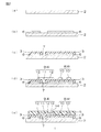
図1は、本発明の配線回路基板の一実施形態を示す回路付サスペンション基板の要部断面図である。
図1において、この回路付サスペンション基板1は、ハードディスクドライブに搭載される回路付サスペンション基板であって、金属支持基板2と、金属支持基板2の上に形成されるベース絶縁層3と、ベース絶縁層3の上に形成される導体パターン4と、導体パターン4を被覆するように、ベース絶縁層3の上に形成されるカバー絶縁層5とを備えている。また、この回路付サスペンション基板1には、金属支持基板2の上に形成され、ベース絶縁層3内に埋設されるグランド層6を備えている。
FIG. 1 is a cross-sectional view of an essential part of a suspension board with circuit showing an embodiment of a wired circuit board of the present invention.
In FIG. 1, a suspension board with
金属支持基板2は、長手方向(図1における紙厚方向)に延びる平板からなり、金属箔や金属薄板から形成されている。金属支持基板2を形成する金属としては、例えば、ステンレス、42アロイなどが用いられ、好ましくは、ステンレスが用いられる。また、その厚みは、例えば、15〜30μm、好ましくは、20〜25μmである。
グランド層6は、金属支持基板2の上に、金属支持基板2と接触するように、幅方向(長手方向に直交する方向)に間隔S1を隔てて複数(2つ)形成されている。グランド層6を形成する金属としては、例えば、クロム、銅、金、銀、白金、ニッケル、チタン、ケイ素、マンガン、ジルコニウム、およびそれらの合金、または、それらの酸化物などが用いられる。これらのうち、銅または銅合金が好ましく用いられる。また、グランド層6の厚みは、例えば、2〜10μm、好ましくは、2〜4μmである。また、幅方向において隣接する各グランド層6の間隔S1は、例えば、80〜500μm、好ましくは、120〜300μmである。
The
A plurality of (two)
ベース絶縁層3は、グランド層6を被覆(埋設)するように、金属支持基板2の上に形成されている。ベース絶縁層3には、幅方向において間隔S1を隔てて隣接配置される各グランド層6の間において、接続孔7が、ベース絶縁層3の厚み方向を貫通して、金属支持基板2を露出させるように形成されている。ベース絶縁層3を形成する絶縁体としては、例えば、ポリイミド、ポリエーテルニトリル、ポリエーテルスルホン、ポリエチレンテレフタレート、ポリエチレンナフタレート、ポリ塩化ビニルなどの合成樹脂が用いられる。これらのうち、ポリイミドが好ましく用いられ、感光性ポリイミドがさらに好ましく用いられる。また、その厚みは、例えば、5〜15μmであり、好ましくは、8〜10μmである。また、接続孔7の幅方向の開口長さS2は、例えば、40〜300μm、好ましくは、60〜200μmである。
The
導体パターン4は、電気信号を伝送する信号配線部8と、磁気ヘッドをグランド接続するためのグランド配線部9とを備えている。
信号配線部8は、一方のグランド層6を被覆するベース絶縁層3の上において、一方のグランド層6と厚み方向(上下方向)において対向するように設けられている。この信号配線部8は、幅方向において互いに間隔を隔てて配置され、長手方向に沿って延びる複数(2つ)の信号配線10と、各信号配線10の長手方向両端部に連続する複数の端子(図示せず。)とを備えている。長手方向一端部の端子には、磁気ヘッドの端子が接続されるとともに、長手方向他端部の端子には、外部制御回路の端子が接続される。
The
The
なお、各信号配線10の幅は、例えば、10〜100μm、好ましくは、15〜50μmであり、各信号配線10間の間隔は、例えば、10〜100μm、好ましくは、15〜50μmである。
グランド配線部9は、接続部11と、グランド層対向部12と、グランド端子部13とを一体的に備えている。
In addition, the width | variety of each
The
接続部11は、その下端面が金属支持基板2と直接接触するように、ベース絶縁層3に形成された接続孔7内に充填されている。
グランド層対向部12は、ベース絶縁層3の上に形成され、接続部11から幅方向両外側に延び、幅方向において間隔S1を隔てて隣接配置される各グランド層6の両方と、厚み方向(上下方向)においてベース絶縁層3を介して対向するように設けられている。
The
The ground
グランド端子部13は、磁気ヘッドのグランド端子と接続するために設けられ、後述するカバー絶縁層5のグランド端子開口部14から露出する部分として設けられている。このグランド端子部13は、図1においては、カバー絶縁層5のグランド端子開口部14が、一方のグランド層6と対向するグランド層対向部12が露出するように形成されているため、一方のグランド層6と対向するグランド層対向部12に設けられているが、例えば、カバー絶縁層5のグランド端子開口部14が、接続部11が露出するように形成されている場合には、その接続部11に設けられる。
The
また、導体パターン4を形成する導体としては、例えば、銅、ニッケル、金、はんだ、またはそれらの合金などの金属が用いられる。これらのうち、銅が好ましく用いられる。また、その厚みは、例えば、5〜20μm、好ましくは、7〜15μmである。
カバー絶縁層5は、導体パターン5を被覆するように、ベース絶縁層3の上に形成されている。このカバー絶縁層5には、上記した信号配線部8の端子に対向して、端子開口部(図示せず。)が形成されるとともに、グランド端子部13の形成部分に、グランド端子開口部14が形成されている。
Moreover, as a conductor which forms the
The
また、カバー絶縁層4を形成する絶縁体としては、上記したベース絶縁層3と同様の絶縁体が用いられる。また、その厚みは、例えば、3〜10μm、好ましくは、4〜5μmである。
図2〜図6は、この回路付サスペンション基板1の製造方法の一実施形態を示す製造工程図である。次に、図2〜図6を参照して、この回路付サスペンション基板1を製造する方法について説明する。
Further, as the insulator for forming the insulating
2-6 is a manufacturing process figure which shows one Embodiment of the manufacturing method of this suspension board |
この方法では、まず、図2(a)に示すように、金属支持基板2を用意し、次いで、図2(b)に示すように、その金属支持基板2の上に、グランド層6を形成する。
金属支持基板2の上にグランド層6を形成するには、図3(a)に示すように、金属支持基板2の表面全面に、スパッタリングまたは電解めっきにより、金属薄膜21を形成する。
In this method, first, a
In order to form the
金属薄膜21を形成する金属としては、例えば、上記したグランド層6と同様の金属が用いられ、好ましくは、銅やクロムが用いられる。また、その厚みは、例えば、0.01〜1μm、好ましくは、0.1〜1μmである。金属薄膜21は、金属支持基板2の表面と接触するように、金属支持基板2との密着性の高い金属と、グランド層6の表面と接触するように、グランド層6との密着力の高い金属とを積層することにより、多層で形成することもできる。
As the metal forming the metal
次いで、図3(b)に示すように、めっきレジスト22を、金属薄膜21の上に、上記したグランド層6の反転パターンで形成する。めっきレジスト22の形成は、例えば、ドライフィルムレジストを露光および現像する、公知の方法が用いられる。
その後、図3(c)に示すように、電解めっき、好ましくは、電解銅めっきにより、めっきレジスト22から露出する金属薄膜21の表面に、グランド層6を、上記したように、幅方向に間隔S1を隔てたパターンとして、形成する。
Next, as shown in FIG. 3B, the plating resist 22 is formed on the metal
Thereafter, as shown in FIG. 3C, the
次いで、図3(d)に示すように、めっきレジスト22を、例えば、エッチング(ウェットエッチング)または剥離によって除去した後、図3(e)に示すように、そのめっきレジスト22が形成されていた部分の金属薄膜21を、例えば、エッチング(ウェットエッチング)によって除去する。
これによって、図2(b)に示すように、金属支持基板2の上に、グランド層6が形成される。なお、図2においては、金属薄膜21は省略されている。
Next, as shown in FIG. 3D, after removing the plating resist 22 by, for example, etching (wet etching) or peeling, the plating resist 22 was formed as shown in FIG. The part of the metal
As a result, a
次いで、この方法では、図2(c)に示すように、ベース絶縁層3を、グランド層6を被覆するように、金属支持基板2の上に形成する。
ベース絶縁層3を、グランド層6を被覆するように、金属支持基板2の上に形成するには、例えば、感光性ポリイミドを用いて、金属支持基板2の上に、ベース絶縁層3をパターンとして形成する場合には、まず、図4(a)に示すように、感光性ポリイミド前駆体のワニス(感光性ポリアミック酸樹脂溶液)を、グランド層6を被覆するように、金属支持基板2の全面に塗布し、乾燥して皮膜23を形成する。次いで、図4(b)に示すように、皮膜23を、フォトマスク24を介して露光する。フォトマスク24は、光透過部24aおよび遮光部24bがパターンとして形成されており、遮光部24bが、例えば、皮膜23の周縁部と接続孔7の形成部分とに対向するように配置される。
Next, in this method, as shown in FIG. 2C, the
In order to form the
その後、皮膜23を、必要により露光後加熱した後、図4(c)に示すように、アルカリ現像液などの現像液を用いて、浸漬法やスプレー法などによって現像する。これによって、皮膜23における遮光部24bとの対向部分が溶解して、次いで、図4(d)に示すように、250℃以上に加熱して硬化すれば、金属支持基板2の上に、グランド層6を被覆するように、ポリイミドからなるベース絶縁層3が、接続孔7が形成されるパターンで形成される。なお、図4では、ベース絶縁層3を、ネガ画像で形成したが、ポジ画像で形成することもできる。
Thereafter, the
なお、ベース絶縁層3の形成は、上記の方法に特に制限されず、例えば、予め接続孔7が穿孔された合成樹脂のフィルムを用意して、そのフィルムを、グランド層6を被覆するように、金属支持基板2の上に、接着剤層を介して貼着することもできる。
次いで、この方法では、図2(d)に示すように、ベース絶縁層3の上に、導体パターン4を形成する。導体パターン4は、アディティブ法やサブトラクティブ法などの公知のパターンニング法により、上記した信号配線部8とグランド配線部9とを備えるパターンとして形成する。微細なパターンを形成する観点から、好ましくは、アディティブ法が用いられる。
The formation of the insulating
Next, in this method, a
アディティブ法によって、ベース絶縁層3の上に導体パターン4を形成するには、まず、図5(a)に示すように、ベース絶縁層3の表面およびベース絶縁層3から露出する金属支持基板2の表面に、スパッタリングにより、金属薄膜25を形成する。
金属薄膜25を形成する金属としては、例えば、上記したグランド層6と同様の金属が用いられ、好ましくは、銅やクロムが用いられる。また、その厚みは、例えば、0.01〜1μm、好ましくは、0.1〜1μmである。好ましくは、金属支持基板2およびベース絶縁層3の表面と接触するように、金属支持基板2およびベース絶縁層3との密着性の高い金属、例えば、クロムと、導体パターン4の表面と接触するように、導体パターン4との密着力の高い金属、例えば、銅とを、順次積層することにより、多層で形成する。
In order to form the
As a metal for forming the metal
次いで、図5(b)に示すように、めっきレジスト26を、金属薄膜25の上に、上記した導体パターン4の反転パターンで形成する。めっきレジスト26の形成は、例えば、ドライフィルムレジストを露光および現像する、公知の方法が用いられる。
その後、図5(c)に示すように、電解めっき、好ましくは、電解銅めっきにより、めっきレジスト26から露出する金属薄膜25の表面に、導体パターン4を、上記した信号配線部8とグランド配線部9とを備えるパターンとして、形成する。
Next, as shown in FIG. 5B, the plating resist 26 is formed on the metal
Thereafter, as shown in FIG. 5C, the
なお、電解めっきにより、信号配線部8がベース絶縁層3の上に形成されると同時に、グランド配線部9が、まず、接続部11が接続孔7内に充填されるように形成され、次いで、グランド層対向部12が接続孔7を囲むベース絶縁層3の上に形成されるようにして、形成される。
次いで、図5(d)に示すように、めっきレジスト26を、例えば、エッチング(ウェットエッチング)または剥離によって除去した後、図6(e)に示すように、そのめっきレジスト26が形成されていた部分の金属薄膜25を、例えば、エッチング(ウェットエッチング)によって除去する。
The
Next, as shown in FIG. 5D, after the plating resist 26 is removed by, for example, etching (wet etching) or peeling, the plating resist 26 is formed as shown in FIG. 6E. The portion of the metal
これによって、図2(d)に示すように、ベース絶縁層3の上に導体パターン4が形成される。なお、図2においては、金属薄膜25は省略されている。
そして、この方法では、図2(e)に示すように、カバー絶縁層5を、導体パターン4を被覆するように、ベース絶縁層3の上に形成する。
カバー絶縁層5を、導体パターン4を被覆するように、ベース絶縁層3の上に形成するには、例えば、感光性ポリイミドを用いて、ベース絶縁層3の上に、カバー絶縁層5をパターンとして形成する場合には、まず、図6(a)に示すように、感光性ポリイミド前駆体のワニス(感光性ポリアミック酸樹脂溶液)を、導体パターン4を被覆するように、ベース絶縁層3の表面およびベース絶縁層3から露出する金属支持基板2の表面に塗布し、乾燥して皮膜27を形成する。次いで、図6(b)に示すように、皮膜27を、フォトマスク28を介して露光する。フォトマスク28は、光透過部28aおよび遮光部28bがパターンとして形成されており、遮光部28bが、例えば、皮膜27の周縁部と、信号配線部8の端子開口部の形成部分と、グランド端子開口部14の形成部分とに対向するように配置される。
As a result, a
In this method, as shown in FIG. 2 (e), the insulating
In order to form the insulating
その後、皮膜27を、必要により露光後加熱した後、図6(c)に示すように、アルカリ現像液などの現像液を用いて、浸漬法やスプレー法などによって現像する。これによって、皮膜27における遮光部28bとの対向部分が溶解して、次いで、図6(d)に示すように、250℃以上に加熱して硬化すれば、ベース絶縁層3の上に、導体パターン4を被覆するように、ポリイミドからなるカバー絶縁層5が、信号配線部8の端子開口部およびグランド端子開口部14が形成されるパターンで形成される。なお、図6では、カバー絶縁層5を、ネガ画像で形成したが、ポジ画像で形成することもできる。
Thereafter, the
なお、カバー絶縁層5の形成は、上記の方法に特に制限されず、例えば、予め信号配線部8の端子開口部およびグランド端子開口部14が穿孔された合成樹脂のフィルムを用意して、そのフィルムを、導体パターン4を被覆するように、ベース絶縁層3の上に、接着剤層を介して貼着することもできる。
このようにして得られる回路付サスペンション基板1では、グランド配線部9のグランド層対向部12が、幅方向において間隔S1を隔てて隣接配置される各グランド層6の両方と、厚み方向(上下方向)において対向配置されている。そのため、導体パターン4を、信号配線部8およびグランド配線部9を高密度で配置する微細パターンとして形成することができる。しかも、グランド配線部9の接続部11は、グランド層6と接続されるのではなく、金属支持基板2と直接(グランド層6を介する間接ではなく直接)接続されているので、グランド配線部9の接続部11とグランド層6との接続部分(界面)での密着性の向上を図ることができ、グランド配線部9を確実にグランド接続することができる。
The formation of the insulating
In the suspension board with
とりわけ、上記した製造方法において、導体パターン4をアディティブ法により形成すると、グランド配線部9の接続部11と金属支持基板2との界面には、金属薄膜25が介在される(図5(e)参照)。
一方、導体パターン4をアディティブ法により形成する場合に、グランド配線部9の接続部11をグランド層6に接続すると、グランド配線部9の接続部11とグランド層6との界面に、金属薄膜25が介在されることとなり、この金属薄膜25の存在によって、グランド配線部9の接続部11とグランド層6との界面の密着不良が顕著となる場合がある。
In particular, in the manufacturing method described above, when the
On the other hand, when the
すなわち、グランド層6を銅から形成し、金属薄膜25をクロム(下層)/銅(上層)の2層から形成し、導体パターン4(接続部11)を銅から形成する場合には、グランド層6と金属薄膜25との間で密着不良を生じて、その結果、グランド配線部9の接続部11とグランド層6との界面の密着不良が顕著となる。
しかし、この回路付サスペンション基板1のように、グランド配線部9の接続部11を金属支持基板2と直接接続すれば、たとえ、グランド配線部9の接続部11と金属支持基板2との界面に、金属薄膜25が介在しても、グランド配線部9の接続部11と金属支持基板2との界面の密着性の向上を図ることができる。
That is, when the
However, if the
すなわち、金属支持基板2をステンレスから形成し、金属薄膜25をクロム(下層)/銅(上層)の2層から形成し、導体パターン4(接続部11)を銅から形成する場合には、金属支持基板2と金属薄膜25との間で密着性が向上し、その結果、グランド配線部9の接続部11と金属支持基板2との界面の密着性の向上を図ることができる。
その結果、この回路付サスペンション基板1では、高密度化および高速化に対応しつつ、十分な信頼性をもって、ノイズの発生を低減することができる。
That is, when the
As a result, the suspension board with
図7は、本発明の配線回路基板の他の実施形態を示す回路付サスペンション基板の要部断面図である。
図7に示すように、回路付サスペンション基板1では、さらに、金属支持基板2に、信号配線部8の信号配線10と厚み方向(上下方向)において対向するように、開口部15を形成することもできる。開口部15を形成することにより、導体パターン4の特性インピーダンスを調整し、部分的にフレキシブル性を向上させることができる。
FIG. 7 is a cross-sectional view of an essential part of a suspension board with circuit showing another embodiment of the wired circuit board of the present invention.
As shown in FIG. 7, in the suspension board with
この開口部15は、特に限定されないが、図7においては、例えば、金属支持基板2において、複数(2つ)の信号配線10と厚み方向(上下方向)において対向する一方のグランド層6との対向部分を、厚み方向に貫通するように形成されている。また、開口部15は、他方のグランド層6との対向部分にも、厚み方向に貫通するように形成されている。
Although the
また、図7に示す回路付サスペンション基板1では、グランド層6を開口部15から被覆するように、絶縁保護層16が設けられている。この絶縁保護層16は、一方のグランド層6と他方のグランド層6とに対応して、それぞれ設けられている。
一方のグランド層6に対応する一方の絶縁保護層16は、幅方向一端部から幅方向他端部に向かって、開口部15を被覆するまで延び、幅方向一端部においては、金属支持基板2とベース絶縁層3との間に介在され、その幅方向内側においては、開口部15を含む金属支持基板2とグランド層6との間に介在されている。また、一方の絶縁保護層16の幅方向他端部は、一方のグランド層6の幅方向途中に配置されており、これによって、一方のグランド層6の幅方向他端部と金属支持基板2との接触が確保されている。
Further, in the suspension board with
One insulating
他方のグランド層6に対応する他方の絶縁保護層16は、幅方向他端部から幅方向一端部に向かって、開口部15を被覆するまで延び、幅方向他端部においては、金属支持基板2とベース絶縁層3との間に介在され、その幅方向内側においては、開口部15を含む金属支持基板2とグランド層6との間に介在されている。また、他方の絶縁保護層16の幅方向一端部は、他方のグランド層6の幅方向途中に配置されており、これによって、他方のグランド層6の幅方向一端部と金属支持基板2との接触が確保されている。
The other insulating
また、絶縁保護層16を形成する絶縁体としては、上記したベース絶縁層3と同様の絶縁体が用いられる。また、その厚みは、例えば、1〜10μm、好ましくは、1〜3μmである。
このような絶縁保護層16を形成することによって、ベース絶縁層3内に埋設されるグランド層6が開口部15から露出することを防止することができ、グランド層6の腐食などを防止することができる。
Further, as the insulator for forming the insulating
By forming such an insulating
図8は、図7に示す回路付サスペンション基板1の製造方法の一実施形態を示す製造工程図である。次に、図7を参照して、図7に示す回路付サスペンション基板1を製造する方法について説明する。
この方法では、まず、図8(a)に示すように、金属支持基板2を用意し、次いで、図8(b)に示すように、その金属支持基板2の上に、絶縁保護層16を形成する。
FIG. 8 is a manufacturing process diagram showing an embodiment of a manufacturing method of the suspension board with
In this method, first, a
金属支持基板2の上に絶縁保護層16を形成するには、まず、金属支持基板2の全面に、感光性ポリイミド前駆体のワニス(感光性ポリアミック酸樹脂溶液)を塗布し、乾燥して皮膜した後、ベース絶縁層3の形成と同様に、露光および現像することにより、上記した絶縁保護層16の形成位置において、ポリイミドからなる絶縁保護層16をパターンとして形成する。
In order to form the insulating
次いで、図8(c)に示すように、絶縁保護層16の幅方向外端部が露出するように、グランド層6を、上記と同様の方法により、絶縁保護層16および金属支持基板2の上に形成する。これによって、絶縁保護層16が、グランド層6によって、幅方向外端部が露出するように、部分的に被覆される。
その後、図8(d)に示すように、上記と同様の方法により、ベース絶縁層3を、グランド層6を被覆するように、金属支持基板2および絶縁保護層16の上に形成し、次いで、図8(e)に示すように、上記と同様の方法により、ベース絶縁層3の上に、信号配線部8とグランド配線部9とを備えるパターンとして、導体パターン4を形成する。
Next, as shown in FIG. 8C, the
Thereafter, as shown in FIG. 8D, the
次いで、図8(f)に示すように、上記と同様の方法により、カバー絶縁層5を、導体パターン4を被覆するように、ベース絶縁層3の上に形成した後、図8(g)に示すように、金属支持基板2に開口部15を形成して、回路付サスペンション基板1を得る。
金属支持基板2に開口部15を形成するには、例えば、金属支持基板2における、開口部15を形成する部分を除く部分に、エッチングレジストを形成した後、エッチングレジストから露出する金属支持基板2を、例えば、塩化第二鉄水溶液などのエッチング液を用いて、浸漬法またはスプレー法によって、化学エッチング(ウェットエッチング)し、その後、エッチングレジストを除去する。
Next, as shown in FIG. 8 (f), the insulating
In order to form the
このようにして得られる図7に示す回路付サスペンション基板1では、上記した図1に示す回路付サスペンション基板1の利点に加えて、開口部15の形成により、導体パターン4の特性インピーダンスを調整し、部分的にフレキシブル性を向上させることができ、さらに、グランド層6を開口部15から被覆するように、絶縁保護層16が設けられているので、ベース絶縁層3内に埋設されるグランド層6が開口部15から露出することを防止することができ、グランド層6の腐食などを防止することができる。
In the suspension board with
なお、上記した回路付サスペンション基板1では、グランド層6の表面および導体パターン4の表面に保護皮膜を設けることもできる。保護皮膜は、上記の製造方法において、グランド層6の形成後、または、導体パターン4の形成後に、それぞれ、例えば、無電解ニッケルめっきによって、ニッケル皮膜として形成することができる。
また、上記の説明では、本発明の配線回路基板を、回路付サスペンション基板を例示して説明したが、本発明の配線回路基板は、回路付サスペンション基板に限らず、例えば、補強層(金属支持基板に相当)を備えるフレキシブル配線回路基板(片面フレキシブル配線回路基板、両面フレキシブル配線回路基板および多層フレキシブル配線回路基板を含む。)なども含んでいる。
In the suspension board with
In the above description, the wired circuit board of the present invention has been described by exemplifying the suspension board with circuit. However, the wired circuit board of the present invention is not limited to the suspension board with circuit, for example, a reinforcing layer (metal support) A flexible wiring circuit board (corresponding to a substrate) (including a single-sided flexible wiring circuit board, a double-sided flexible wiring circuit board, and a multilayer flexible wiring circuit board).
以下に実施例および比較例を示し、本発明をさらに具体的に説明するが、本発明は、何らこれら実施例および比較例に限定されることはない。
実施例1
金属支持基板として、厚み25μmのステンレス基板を用意して(図2(a)参照)、その金属支持基板の上に、金属薄膜として、厚み0.03μmのクロム薄膜と厚み0.07μmの銅薄膜とをスパッタリングによって順次形成した(図3(a)参照)。次いで、グランド層の反転パターンでめっきレジストを、ドライフィルムレジストを用いて形成した(図3(b)参照)。その後、めっきレジストから露出する金属薄膜の表面に、グランド層として、厚み4.0μmの銅箔を、硫酸銅水溶液を用いて電解銅めっきにより形成した(図3(c)参照)。なお、この銅箔は、幅方向に間隔を隔てて2つ形成した。
EXAMPLES The present invention will be described more specifically below with reference to examples and comparative examples, but the present invention is not limited to these examples and comparative examples.
Example 1
A stainless steel substrate having a thickness of 25 μm is prepared as a metal support substrate (see FIG. 2A), and a chromium thin film having a thickness of 0.03 μm and a copper thin film having a thickness of 0.07 μm are formed on the metal support substrate as metal thin films. Were sequentially formed by sputtering (see FIG. 3A). Next, a plating resist was formed using a dry film resist with a reverse pattern of the ground layer (see FIG. 3B). Thereafter, a copper foil having a thickness of 4.0 μm was formed on the surface of the metal thin film exposed from the plating resist by electrolytic copper plating using an aqueous copper sulfate solution (see FIG. 3C). Two copper foils were formed at an interval in the width direction.
次いで、めっきレジストを、水酸化ナトリウム水溶液を用いて剥離により除去した後(図3(d)参照)、めっきレジストが形成されていた部分の金属薄膜をエッチングにより除去し(図3(e)参照)、グランド層の表面に、保護皮膜として、厚み0.1μmのニッケル皮膜を無電解ニッケルめっきにより形成した。
次いで、グランド層を被覆するように、金属支持基板の上に、感光性ポリアミック酸樹脂のワニスを塗布後、乾燥して皮膜を形成し(図4(a)参照)、その皮膜を露光(図4(b)参照)および現像(図4(c)参照)し、さらに加熱硬化することにより(図4(d)参照)、接続孔が形成されるパターンとして、厚み10μmのポリイミドからなるベース絶縁層を形成した(図2(c)参照)。
Next, after removing the plating resist by peeling off using a sodium hydroxide aqueous solution (see FIG. 3 (d)), the metal thin film where the plating resist was formed is removed by etching (see FIG. 3 (e)). ) A nickel film having a thickness of 0.1 μm was formed on the surface of the ground layer by electroless nickel plating as a protective film.
Next, a varnish of a photosensitive polyamic acid resin is applied on the metal support substrate so as to cover the ground layer, and then dried to form a film (see FIG. 4A), and the film is exposed (see FIG. 4). 4 (b)) and development (see FIG. 4 (c)), followed by heat-curing (see FIG. 4 (d)), a base insulation made of polyimide having a thickness of 10 μm as a pattern for forming connection holes. A layer was formed (see FIG. 2C).
次いで、ベース絶縁層の表面および接続孔から露出する金属支持基板の表面に、金属薄膜として、厚み0.03μmのクロム薄膜と厚み0.07μmの銅薄膜とをスパッタリングによって順次形成した(図5(a)参照)。次いで、導体パターンの反転パターンでめっきレジストを、ドライフィルムレジストを用いて形成した(図5(b)参照)。その後、めっきレジストから露出する金属薄膜の表面に、導体パターンとして、厚み10μmの銅箔を、硫酸銅水溶液を用いて電解銅めっきにより形成した(図5(c)参照)。 Next, a chromium thin film having a thickness of 0.03 μm and a copper thin film having a thickness of 0.07 μm were sequentially formed by sputtering on the surface of the base insulating layer and the surface of the metal supporting substrate exposed from the connection holes (FIG. 5 ( a)). Next, a plating resist was formed using a dry film resist with a reverse pattern of the conductor pattern (see FIG. 5B). Thereafter, a copper foil having a thickness of 10 μm was formed as a conductive pattern on the surface of the metal thin film exposed from the plating resist by electrolytic copper plating using an aqueous copper sulfate solution (see FIG. 5C).
次いで、めっきレジストを、水酸化ナトリウム水溶液を用いて剥離により除去した後(図5(d)参照)、めっきレジストが形成されていた部分の金属薄膜をエッチングにより除去し(図5(e)参照)、導体パターンの表面に、保護皮膜として、厚み0.1μmのニッケル皮膜を無電解ニッケルめっきにより形成した。なお、この導体パターンは、上記した信号配線部とグランド配線部とを備えるパターンとして形成された。 Next, after removing the plating resist by peeling off using a sodium hydroxide aqueous solution (see FIG. 5D), the metal thin film in the portion where the plating resist was formed is removed by etching (see FIG. 5E). ) A nickel film having a thickness of 0.1 μm was formed on the surface of the conductor pattern by electroless nickel plating as a protective film. In addition, this conductor pattern was formed as a pattern provided with the above-mentioned signal wiring part and ground wiring part.
その後、導体パターンを被覆するように、金属支持基板およびカバー絶縁層の上に、感光性ポリアミック酸樹脂のワニスを塗布後、乾燥して皮膜を形成し(図6(a)参照)、その皮膜を露光(図6(b)参照)および現像(図6(c)参照)し、さらに加熱硬化することにより(図6(d)参照)、信号配線部8の端子開口部、および、グランド端子開口部14が形成されるパターンとして、厚み5μmのポリイミドからなるカバー絶縁層を形成し、これによって、回路付サスペンション基板を得た(図2(e)参照)。
Thereafter, a varnish of photosensitive polyamic acid resin is applied on the metal support substrate and the insulating cover layer so as to cover the conductor pattern, and then dried to form a film (see FIG. 6A). Is exposed (see FIG. 6 (b)) and developed (see FIG. 6 (c)), and further heat-cured (see FIG. 6 (d)), the terminal opening of the
実施例2
金属支持基板として、厚み25μmのステンレス基板を用意して(図8(a)参照)、その金属支持基板の上に、感光性ポリアミック酸樹脂のワニスを塗布後、乾燥して皮膜を形成し、その皮膜を露光および現像し、さらに加熱硬化することにより、上記した絶縁保護層の形成位置において、厚み2μmのポリイミドからなる絶縁保護層をパターンとして形成した(図8(b)参照)。
Example 2
As a metal support substrate, a stainless steel substrate having a thickness of 25 μm is prepared (see FIG. 8A), a varnish of photosensitive polyamic acid resin is applied on the metal support substrate, and then dried to form a film. The film was exposed and developed, and further heat-cured to form an insulating protective layer made of polyimide having a thickness of 2 μm as a pattern at the position where the insulating protective layer was formed (see FIG. 8B).
次いで、各絶縁保護層の幅方向外端部が露出するように、厚み4.0μmの銅箔からなるグランド層を、実施例1と同様の方法により、絶縁保護層および金属支持基板の上に形成した(図8(c)参照)。
その後、実施例1と同様の方法により、厚み10μmのポリイミドからなるベース絶縁層を、グランド層を被覆するように、金属支持基板および絶縁保護層の上に形成し(図8(d)参照)、次いで、実施例1と同様の方法により、ベース絶縁層の上に、信号配線部とグランド配線部とを備えるパターンとして、厚み10μmの銅箔からなる導体パターンを形成した(図8(e)参照)。
Next, a ground layer made of a copper foil having a thickness of 4.0 μm is formed on the insulating protective layer and the metal supporting substrate in the same manner as in Example 1 so that the outer ends in the width direction of each insulating protective layer are exposed. It formed (refer FIG.8 (c)).
Thereafter, a base insulating layer made of polyimide having a thickness of 10 μm is formed on the metal supporting substrate and the insulating protective layer so as to cover the ground layer by the same method as in Example 1 (see FIG. 8D). Then, a conductor pattern made of a copper foil having a thickness of 10 μm was formed on the insulating base layer as a pattern having a signal wiring portion and a ground wiring portion by the same method as in Example 1 (FIG. 8E). reference).
次いで、実施例1と同様の方法により、厚み5μmのポリイミドからなるカバー絶縁層を、導体パターンを被覆するように、ベース絶縁層の上に形成した後(図8(f)参照)、金属支持基板を、塩化第二鉄水溶液を用いてエッチングすることにより、開口部を形成して、回路付サスペンション基板を得た(図8(g)参照)。 Next, an insulating cover layer made of polyimide having a thickness of 5 μm was formed on the insulating base layer so as to cover the conductor pattern by the same method as in Example 1 (see FIG. 8F), and then supported by metal. The substrate was etched using a ferric chloride aqueous solution to form openings, and a suspension board with circuit was obtained (see FIG. 8G).
1 回路付サスペンション基板
2 金属支持基板
3 ベース絶縁層
4 導体パターン
5 カバー絶縁層
6 グランド層
8 信号配線部
9 グランド配線部
11 接続部
12 グランド層対向部
14 グランド端子開口部
15 絶縁保護層
25 金属薄膜
DESCRIPTION OF
Claims (5)
前記金属支持基板の上に形成されるベース絶縁層と、
前記ベース絶縁層の上に形成され、電気信号を伝送する信号配線部およびグランド接続のためのグランド配線部を含む導体パターンと、
前記導体パターンを被覆するように、前記ベース絶縁層の上に形成されるカバー絶縁層と、
前記信号配線部の少なくとも一部と厚み方向において対向し、少なくとも一部が前記金属支持基板に接続されるように、前記ベース絶縁層内に埋設されるグランド層とを備え、
前記グランド配線部は、前記グランド層の少なくとも一部と厚み方向において対向するグランド層対向部と、前記金属支持基板と接続される接続部とを含んでいることを特徴とする、配線回路基板。 A metal support substrate;
A base insulating layer formed on the metal support substrate;
A conductor pattern formed on the insulating base layer and including a signal wiring portion for transmitting an electrical signal and a ground wiring portion for ground connection;
An insulating cover layer formed on the insulating base layer so as to cover the conductive pattern;
A ground layer embedded in the insulating base layer so as to be opposed to at least a part of the signal wiring part in the thickness direction and to be connected to the metal supporting substrate at least a part of the signal wiring part;
The wired circuit board, wherein the ground wiring part includes a ground layer facing part facing at least a part of the ground layer in a thickness direction, and a connection part connected to the metal supporting board.
前記グランド層対向部が、前記間隔を隔てて配置される各前記グランド層の少なくともいずれか一方と厚み方向において対向するように配置され、
前記接続部が、前記間隔を隔てて配置される各前記グランド層の間に配置されていることを特徴とする、請求項1に記載の配線回路基板。 The ground layer is provided at an interval in a direction orthogonal to the direction in which the signal wiring portion extends,
The ground layer facing portion is disposed so as to face at least one of the ground layers disposed at an interval in the thickness direction,
The wired circuit board according to claim 1, wherein the connection portion is disposed between the ground layers disposed at a distance from each other.
Priority Applications (1)
| Application Number | Priority Date | Filing Date | Title |
|---|---|---|---|
| JP2005272498A JP4611159B2 (en) | 2005-09-20 | 2005-09-20 | Printed circuit board |
Applications Claiming Priority (1)
| Application Number | Priority Date | Filing Date | Title |
|---|---|---|---|
| JP2005272498A JP4611159B2 (en) | 2005-09-20 | 2005-09-20 | Printed circuit board |
Publications (2)
| Publication Number | Publication Date |
|---|---|
| JP2007088056A true JP2007088056A (en) | 2007-04-05 |
| JP4611159B2 JP4611159B2 (en) | 2011-01-12 |
Family
ID=37974769
Family Applications (1)
| Application Number | Title | Priority Date | Filing Date |
|---|---|---|---|
| JP2005272498A Active JP4611159B2 (en) | 2005-09-20 | 2005-09-20 | Printed circuit board |
Country Status (1)
| Country | Link |
|---|---|
| JP (1) | JP4611159B2 (en) |
Cited By (13)
| Publication number | Priority date | Publication date | Assignee | Title |
|---|---|---|---|---|
| JP2008282995A (en) * | 2007-05-10 | 2008-11-20 | Nitto Denko Corp | Wiring circuit board |
| JP2009260056A (en) * | 2008-04-17 | 2009-11-05 | Nitto Denko Corp | Wiring circuit board, and method of manufacturing the same |
| JP2009259315A (en) * | 2008-04-14 | 2009-11-05 | Nitto Denko Corp | Suspension board with circuit and production method thereof |
| JP2011198814A (en) * | 2010-03-17 | 2011-10-06 | Dainippon Printing Co Ltd | Wiring circuit board and method of manufacturing wiring circuit board |
| US8134080B2 (en) | 2005-07-07 | 2012-03-13 | Nitto Denko Corporation | Wired circuit board |
| US8266794B2 (en) | 2006-08-30 | 2012-09-18 | Nitto Denko Corporation | Method of producing a wired circuit board |
| JP2013033569A (en) * | 2011-08-02 | 2013-02-14 | Dainippon Printing Co Ltd | Substrate for suspension, suspension, suspension with element, hard disk drive, and method for manufacturing substrate for suspension |
| JP2016042405A (en) * | 2015-11-04 | 2016-03-31 | 大日本印刷株式会社 | Suspension substrate, suspension, suspension with element, and hard disk drive |
| JP2016531407A (en) * | 2013-08-23 | 2016-10-06 | アップル インコーポレイテッド | Connector insert and receptacle tongue formed using a printed circuit board |
| JP2017208443A (en) * | 2016-05-18 | 2017-11-24 | 日東電工株式会社 | Wiring-circuit board and method for manufacturing the same |
| CN107801294A (en) * | 2016-09-06 | 2018-03-13 | 日东电工株式会社 | Wired circuit board and its manufacture method |
| JP2021028988A (en) * | 2020-11-13 | 2021-02-25 | 日東電工株式会社 | Wiring-circuit board and method for manufacturing the same |
| WO2023281712A1 (en) * | 2021-07-08 | 2023-01-12 | 日本たばこ産業株式会社 | Power supply unit for aerosol generator |
Citations (5)
| Publication number | Priority date | Publication date | Assignee | Title |
|---|---|---|---|---|
| JPH09282624A (en) * | 1996-04-09 | 1997-10-31 | Tdk Corp | Bead gimbal assembly and hard disk drive device provided with it |
| JPH10507028A (en) * | 1995-06-09 | 1998-07-07 | インターナシヨナル・ビジネス・マシーンズ・コーポレーシヨン | Integrated head / electronic circuit interconnect suspension for data recording disk drive |
| JP2003228934A (en) * | 2002-02-01 | 2003-08-15 | Fujitsu Ltd | Suspension structure |
| JP2005011387A (en) * | 2003-06-16 | 2005-01-13 | Hitachi Global Storage Technologies Inc | Magnetic disk unit |
| JP2005100488A (en) * | 2003-09-22 | 2005-04-14 | Nitto Denko Corp | Suspension substrate with circuit and its manufacturing method |
-
2005
- 2005-09-20 JP JP2005272498A patent/JP4611159B2/en active Active
Patent Citations (5)
| Publication number | Priority date | Publication date | Assignee | Title |
|---|---|---|---|---|
| JPH10507028A (en) * | 1995-06-09 | 1998-07-07 | インターナシヨナル・ビジネス・マシーンズ・コーポレーシヨン | Integrated head / electronic circuit interconnect suspension for data recording disk drive |
| JPH09282624A (en) * | 1996-04-09 | 1997-10-31 | Tdk Corp | Bead gimbal assembly and hard disk drive device provided with it |
| JP2003228934A (en) * | 2002-02-01 | 2003-08-15 | Fujitsu Ltd | Suspension structure |
| JP2005011387A (en) * | 2003-06-16 | 2005-01-13 | Hitachi Global Storage Technologies Inc | Magnetic disk unit |
| JP2005100488A (en) * | 2003-09-22 | 2005-04-14 | Nitto Denko Corp | Suspension substrate with circuit and its manufacturing method |
Cited By (19)
| Publication number | Priority date | Publication date | Assignee | Title |
|---|---|---|---|---|
| US8134080B2 (en) | 2005-07-07 | 2012-03-13 | Nitto Denko Corporation | Wired circuit board |
| US8266794B2 (en) | 2006-08-30 | 2012-09-18 | Nitto Denko Corporation | Method of producing a wired circuit board |
| US8760815B2 (en) | 2007-05-10 | 2014-06-24 | Nitto Denko Corporation | Wired circuit board |
| JP2008282995A (en) * | 2007-05-10 | 2008-11-20 | Nitto Denko Corp | Wiring circuit board |
| JP2009259315A (en) * | 2008-04-14 | 2009-11-05 | Nitto Denko Corp | Suspension board with circuit and production method thereof |
| JP2009260056A (en) * | 2008-04-17 | 2009-11-05 | Nitto Denko Corp | Wiring circuit board, and method of manufacturing the same |
| JP2011198814A (en) * | 2010-03-17 | 2011-10-06 | Dainippon Printing Co Ltd | Wiring circuit board and method of manufacturing wiring circuit board |
| JP2013033569A (en) * | 2011-08-02 | 2013-02-14 | Dainippon Printing Co Ltd | Substrate for suspension, suspension, suspension with element, hard disk drive, and method for manufacturing substrate for suspension |
| US9992863B2 (en) | 2013-08-23 | 2018-06-05 | Apple Inc. | Connector inserts and receptacle tongues formed using printed circuit boards |
| JP2016531407A (en) * | 2013-08-23 | 2016-10-06 | アップル インコーポレイテッド | Connector insert and receptacle tongue formed using a printed circuit board |
| JP2016042405A (en) * | 2015-11-04 | 2016-03-31 | 大日本印刷株式会社 | Suspension substrate, suspension, suspension with element, and hard disk drive |
| CN107404800A (en) * | 2016-05-18 | 2017-11-28 | 日东电工株式会社 | Wired circuit board and its manufacture method |
| JP2017208443A (en) * | 2016-05-18 | 2017-11-24 | 日東電工株式会社 | Wiring-circuit board and method for manufacturing the same |
| CN107801294A (en) * | 2016-09-06 | 2018-03-13 | 日东电工株式会社 | Wired circuit board and its manufacture method |
| JP2018041795A (en) * | 2016-09-06 | 2018-03-15 | 日東電工株式会社 | Wiring-circuit board and method for manufacturing the same |
| JP2021028988A (en) * | 2020-11-13 | 2021-02-25 | 日東電工株式会社 | Wiring-circuit board and method for manufacturing the same |
| JP7021329B2 (en) | 2020-11-13 | 2022-02-16 | 日東電工株式会社 | Wiring circuit board and its manufacturing method |
| WO2023281712A1 (en) * | 2021-07-08 | 2023-01-12 | 日本たばこ産業株式会社 | Power supply unit for aerosol generator |
| JP7470870B2 (en) | 2021-07-08 | 2024-04-18 | 日本たばこ産業株式会社 | Aerosol generator power supply unit |
Also Published As
| Publication number | Publication date |
|---|---|
| JP4611159B2 (en) | 2011-01-12 |
Similar Documents
| Publication | Publication Date | Title |
|---|---|---|
| JP4611159B2 (en) | Printed circuit board | |
| JP4403090B2 (en) | Printed circuit board | |
| JP4339834B2 (en) | Method for manufacturing suspension board with circuit | |
| JP4799902B2 (en) | Wiring circuit board and method for manufacturing wiring circuit board | |
| JP4865453B2 (en) | Wiring circuit board and manufacturing method thereof | |
| JP4308862B2 (en) | Wiring circuit board and manufacturing method thereof | |
| TWI665943B (en) | Multi-layer flexible printed wiring board and manufacturing method thereof | |
| US8134080B2 (en) | Wired circuit board | |
| JP4790558B2 (en) | Method for manufacturing printed circuit board | |
| JP2009129490A (en) | Wired circuit board | |
| JP4588622B2 (en) | Method for manufacturing printed circuit board | |
| JP5829100B2 (en) | Printed circuit board | |
| JP4887232B2 (en) | Method for manufacturing printed circuit board | |
| TW200412205A (en) | Double-sided printed circuit board without via holes and method of fabricating the same | |
| JP2007157836A (en) | Wiring circuit board | |
| JP2006040414A (en) | Wiring circuit board | |
| JP2009016610A (en) | Wiring circuit substrate and its manufacturing method | |
| JP4796121B2 (en) | Wiring circuit board connection structure | |
| JP2007115321A (en) | Wiring circuit board | |
| JP4640853B2 (en) | Printed circuit board | |
| JP4128998B2 (en) | Wiring circuit board and manufacturing method thereof | |
| JP4588405B2 (en) | Wiring circuit board and manufacturing method thereof | |
| JP2006165269A (en) | Wiring circuit board | |
| JP2006128291A (en) | Multilayered printed wiring board, manufacturing method thereof and electronic device | |
| JP4566778B2 (en) | Printed circuit board |
Legal Events
| Date | Code | Title | Description |
|---|---|---|---|
| A621 | Written request for application examination |
Free format text: JAPANESE INTERMEDIATE CODE: A621 Effective date: 20070411 |
|
| A977 | Report on retrieval |
Free format text: JAPANESE INTERMEDIATE CODE: A971007 Effective date: 20100318 |
|
| A131 | Notification of reasons for refusal |
Free format text: JAPANESE INTERMEDIATE CODE: A131 Effective date: 20100323 |
|
| A521 | Request for written amendment filed |
Free format text: JAPANESE INTERMEDIATE CODE: A523 Effective date: 20100520 |
|
| TRDD | Decision of grant or rejection written | ||
| A01 | Written decision to grant a patent or to grant a registration (utility model) |
Free format text: JAPANESE INTERMEDIATE CODE: A01 Effective date: 20101012 |
|
| A01 | Written decision to grant a patent or to grant a registration (utility model) |
Free format text: JAPANESE INTERMEDIATE CODE: A01 |
|
| A61 | First payment of annual fees (during grant procedure) |
Free format text: JAPANESE INTERMEDIATE CODE: A61 Effective date: 20101013 |
|
| FPAY | Renewal fee payment (event date is renewal date of database) |
Free format text: PAYMENT UNTIL: 20131022 Year of fee payment: 3 |
|
| R150 | Certificate of patent or registration of utility model |
Ref document number: 4611159 Country of ref document: JP Free format text: JAPANESE INTERMEDIATE CODE: R150 Free format text: JAPANESE INTERMEDIATE CODE: R150 |
|
| FPAY | Renewal fee payment (event date is renewal date of database) |
Free format text: PAYMENT UNTIL: 20131022 Year of fee payment: 3 |
|
| FPAY | Renewal fee payment (event date is renewal date of database) |
Free format text: PAYMENT UNTIL: 20161022 Year of fee payment: 6 |
|
| R250 | Receipt of annual fees |
Free format text: JAPANESE INTERMEDIATE CODE: R250 |
|
| R250 | Receipt of annual fees |
Free format text: JAPANESE INTERMEDIATE CODE: R250 |
|
| R250 | Receipt of annual fees |
Free format text: JAPANESE INTERMEDIATE CODE: R250 |
|
| R250 | Receipt of annual fees |
Free format text: JAPANESE INTERMEDIATE CODE: R250 |
|
| R250 | Receipt of annual fees |
Free format text: JAPANESE INTERMEDIATE CODE: R250 |
|
| R250 | Receipt of annual fees |
Free format text: JAPANESE INTERMEDIATE CODE: R250 |
|
| R250 | Receipt of annual fees |
Free format text: JAPANESE INTERMEDIATE CODE: R250 |
|
| R250 | Receipt of annual fees |
Free format text: JAPANESE INTERMEDIATE CODE: R250 |
|
| R250 | Receipt of annual fees |
Free format text: JAPANESE INTERMEDIATE CODE: R250 |