JP2007060214A - Piezoelectric device - Google Patents
Piezoelectric device Download PDFInfo
- Publication number
- JP2007060214A JP2007060214A JP2005242243A JP2005242243A JP2007060214A JP 2007060214 A JP2007060214 A JP 2007060214A JP 2005242243 A JP2005242243 A JP 2005242243A JP 2005242243 A JP2005242243 A JP 2005242243A JP 2007060214 A JP2007060214 A JP 2007060214A
- Authority
- JP
- Japan
- Prior art keywords
- package body
- piezoelectric device
- circuit module
- electrodes
- piezoelectric
- Prior art date
- Legal status (The legal status is an assumption and is not a legal conclusion. Google has not performed a legal analysis and makes no representation as to the accuracy of the status listed.)
- Withdrawn
Links
Images


Classifications
-
- H—ELECTRICITY
- H01—ELECTRIC ELEMENTS
- H01L—SEMICONDUCTOR DEVICES NOT COVERED BY CLASS H10
- H01L2224/00—Indexing scheme for arrangements for connecting or disconnecting semiconductor or solid-state bodies and methods related thereto as covered by H01L24/00
- H01L2224/01—Means for bonding being attached to, or being formed on, the surface to be connected, e.g. chip-to-package, die-attach, "first-level" interconnects; Manufacturing methods related thereto
- H01L2224/10—Bump connectors; Manufacturing methods related thereto
- H01L2224/15—Structure, shape, material or disposition of the bump connectors after the connecting process
- H01L2224/16—Structure, shape, material or disposition of the bump connectors after the connecting process of an individual bump connector
- H01L2224/161—Disposition
- H01L2224/16151—Disposition the bump connector connecting between a semiconductor or solid-state body and an item not being a semiconductor or solid-state body, e.g. chip-to-substrate, chip-to-passive
- H01L2224/16221—Disposition the bump connector connecting between a semiconductor or solid-state body and an item not being a semiconductor or solid-state body, e.g. chip-to-substrate, chip-to-passive the body and the item being stacked
- H01L2224/16225—Disposition the bump connector connecting between a semiconductor or solid-state body and an item not being a semiconductor or solid-state body, e.g. chip-to-substrate, chip-to-passive the body and the item being stacked the item being non-metallic, e.g. insulating substrate with or without metallisation
-
- H—ELECTRICITY
- H01—ELECTRIC ELEMENTS
- H01L—SEMICONDUCTOR DEVICES NOT COVERED BY CLASS H10
- H01L2924/00—Indexing scheme for arrangements or methods for connecting or disconnecting semiconductor or solid-state bodies as covered by H01L24/00
- H01L2924/15—Details of package parts other than the semiconductor or other solid state devices to be connected
- H01L2924/161—Cap
- H01L2924/1615—Shape
- H01L2924/16195—Flat cap [not enclosing an internal cavity]
Abstract
Description
本発明は、圧電振動片及びその他の電子部品をパッケージ内に平面配置にて接合した圧電デバイスに関する。 The present invention relates to a piezoelectric device in which a piezoelectric vibrating piece and other electronic components are joined in a planar arrangement in a package.
従来より、各種情報・通信機器やOA機器、また、民生機器等の電子機器には、圧電振動片を備えた圧電デバイスが使用されている。特に最近は、モバイルコンピュータ、ICカード等の小型情報機器や、携帯電話に代表される携帯型通信機器の分野で、装置の小型化・軽量化と共に高機能化の進展が著しく、これに伴なって、圧電デバイスの小型化・薄型化、及び高機能化が図られている。圧電デバイスの高機能化においては、例えば圧電デバイスの一例としての水晶発振回路には、水晶振動片のみならず、発振回路、周波数調整回路、温度補償回路等を備えていることが望まれている。 Conventionally, a piezoelectric device including a piezoelectric vibrating piece has been used in various information / communication equipment, OA equipment, and electronic equipment such as consumer equipment. In recent years, in particular, in the field of small information devices such as mobile computers and IC cards, and portable communication devices represented by mobile phones, the progress of high functionality along with the downsizing and weight reduction of devices has been remarkable. Thus, the piezoelectric device has been reduced in size, thickness, and functionality. In order to increase the functionality of piezoelectric devices, for example, a crystal oscillation circuit as an example of a piezoelectric device is desired to include not only a crystal resonator element but also an oscillation circuit, a frequency adjustment circuit, a temperature compensation circuit, and the like. .
このような小型化・薄型化、及び高機能化のニーズに応える圧電デバイスとして、圧電振動片とその他の回路を構成する電子部品が同一パッケージ内に備えられた圧電デバイスが提案されている。すなわち、平板状と矩形環状のセラミックからなるセラミックベースを積層して凹部を有するパッケージ本体を形成し、その凹底部の平面上に設けられた接続端子(電極)に、圧電振動片としての水晶板(水晶振動片)と、電子部品としてのチップ抵抗及びチップコンデンサが、それぞれ導電性接着剤により接合され、さらにICがワイヤボンディングにより接合されている。水晶板とそれぞれの電子部品が接合された各接続端子は、セラミックベースの底板に設けられた物理的に充填されたスルーホールにより、底板の外側に形成されたユーザ端子と電気的に接続されている。さらに、上記の水晶板及び各種電子部品が搭載されたセラミックベースの上面にはキャップ(蓋体)が接合され、パッケージ内部を気密に保って封止されている(特許文献1)。なお、上記の導電性接着剤を用いた各電子部品の接合方法の他に、半田付けによる接合が一般的に行なわれている。 As a piezoelectric device that meets the needs for such miniaturization / thinning and high functionality, a piezoelectric device is proposed in which a piezoelectric vibrating piece and other electronic components constituting a circuit are provided in the same package. That is, a package base having a recess is formed by laminating a ceramic base made of a flat plate and a rectangular annular ceramic, and a crystal plate as a piezoelectric vibrating piece is connected to a connection terminal (electrode) provided on the plane of the bottom of the recess (Crystal resonator element), a chip resistor and a chip capacitor as electronic components are respectively bonded by a conductive adhesive, and an IC is further bonded by wire bonding. Each connection terminal where the quartz plate and each electronic component are joined is electrically connected to the user terminal formed outside the bottom plate by a physically filled through hole provided in the bottom plate of the ceramic base. Yes. Furthermore, a cap (lid body) is joined to the upper surface of the ceramic base on which the above-described quartz plate and various electronic components are mounted, and the inside of the package is kept airtight (Patent Document 1). In addition to the above-described electronic component joining method using the conductive adhesive, joining by soldering is generally performed.
しかしながら、特許文献1に記載の圧電デバイスの構造では、パッケージ本体の凹底部に各種電子部品を接合するときに、パッケージ本体を囲む側壁が阻害要因となって作業性が悪い。例えば、導電性接着剤や半田ペーストを塗布する際に使用するディスペンサのニードル部や、電子部品を仮搭載する際に使用するチップマウンタのノズル、またはワイヤボンディングする際のワイヤボンダのキャピラリ等が、パッケージ本体の側壁に緩衝して作業性を悪化させていた。このため、パッケージ本体の凹底部の側壁寄りには電子部品を配置することができず、一定のデッドスペースを設けなければならないという制約が生じ、圧電デバイスの平面方向の小型化に不利となってしまうという問題があった。
本発明は、上記問題を解消するためになされたものであって、その目的は、圧電デバイスの小型化に寄与して且つ組立性を向上し、高機能化が可能な構造の圧電デバイスを提供することにある。
However, in the structure of the piezoelectric device described in
The present invention has been made to solve the above-described problems, and an object of the present invention is to provide a piezoelectric device having a structure that contributes to miniaturization of the piezoelectric device, improves assembling property, and can achieve high functionality. There is to do.
上記課題を解決するために、本発明では、凹部が形成され、この凹部の底部平面上に設けられた複数の電極を有するパッケージ本体と、圧電振動片と、複数の電子部品と、パッケージ本体の凹部内を気密に封止する蓋体と、を備え、圧電振動片及び電子部品が、パッケージ本体の複数の電極に接合されている構造の圧電デバイスであって、電子部品は基板に接合され、該基板が、複数の電極のうちのいずれかに接合されていることを主旨とする。 In order to solve the above problems, in the present invention, a recess is formed, and a package body having a plurality of electrodes provided on a bottom plane of the recess, a piezoelectric vibrating piece, a plurality of electronic components, and a package body A lid that hermetically seals the inside of the recess, and a piezoelectric device having a structure in which the piezoelectric vibrating piece and the electronic component are bonded to the plurality of electrodes of the package body, the electronic component being bonded to the substrate, The main purpose is that the substrate is bonded to any one of the plurality of electrodes.
この構成によれば、従来の、パッケージ本体の凹底部に直接回路素子を搭載する方式の場合に、パッケージ本体の側壁が障害物となって困難であった側壁近傍への各種回路素子の配置が可能となる。この結果、省スペースにて各種回路素子をパッケージ本体の凹底部に搭載することができるので、圧電デバイスの、特に平面方向の小型化を図ることが可能となる。また、各種回路素子を省スペースにて搭載可能であるので、小型なサイズを保持しながら、圧電デバイスの高機能化を図ることが可能となる。さらに、回路素子が搭載された基板は、基板の回路配線設計により汎用性を持たせることも可能であるため、別機種の圧電デバイスに用いることも可能となり、圧電デバイス製造の低コスト化や、新規圧電デバイスの量産化における納期短縮等に寄与することが可能となる。 According to this configuration, in the case of the conventional system in which the circuit element is directly mounted on the concave bottom portion of the package body, the arrangement of various circuit elements in the vicinity of the side wall where the side wall of the package body has become difficult as an obstacle is difficult. It becomes possible. As a result, various circuit elements can be mounted on the concave bottom portion of the package body in a space-saving manner, so that it is possible to reduce the size of the piezoelectric device, particularly in the planar direction. In addition, since various circuit elements can be mounted in a space-saving manner, it is possible to increase the functionality of the piezoelectric device while maintaining a small size. Furthermore, since the board on which the circuit element is mounted can be made versatile by designing the circuit wiring of the board, it can also be used for other types of piezoelectric devices, reducing the cost of manufacturing piezoelectric devices, It is possible to contribute to shortening the delivery time in mass production of new piezoelectric devices.
本発明では、基板に接合された電子部品が樹脂封止されていることが望ましい。 In the present invention, it is desirable that the electronic component bonded to the substrate is resin-sealed.
この構成によれば、基板に接合されている複数の電子部品が封止樹脂によって封止されて、パッケージ本体の凹底部に搭載されている。これにより、例えば、基板に電子部品を半田により接合する際に発生する半田ボールや半田屑などの導電性を有した異物が残留していた場合に、該導電性を有する異物が、圧電振動片やその接続部分に付着して、圧電振動片の振動特性への悪影響を及ぼしたり、電気的な短絡等の原因となる危険性を回避することができる。また、基板や電子部品、及び半田接合に使用されるフラックス等の残留物等が移動若しくは気化するなどして圧電振動片に付着し、振動特性等に悪影響を及ぼす危険性を回避すること等が可能となる。従って、圧電振動片による振動特性に優れ、高信頼性を有する圧電デバイスを提供することが可能となる。 According to this configuration, the plurality of electronic components bonded to the substrate are sealed with the sealing resin and mounted on the concave bottom portion of the package body. Thereby, for example, when conductive foreign matter such as solder balls and solder scraps generated when the electronic component is joined to the substrate by soldering, the conductive foreign matter is transferred to the piezoelectric vibrating piece. In addition, it is possible to avoid a risk of adhering to the connecting portion and adversely affecting the vibration characteristics of the piezoelectric vibrating piece or causing an electrical short circuit. In addition, it is possible to avoid the risk of adversely affecting the vibration characteristics, etc., by adhering to the piezoelectric vibrating piece due to movement or vaporization of residues such as flux used for the substrate, electronic parts, and soldering. It becomes possible. Therefore, it is possible to provide a piezoelectric device having excellent vibration characteristics by the piezoelectric vibrating piece and having high reliability.
(第1の実施形態)
以下、本発明に係る圧電デバイスの第1の実施形態について図面に従って説明する。
(First embodiment)
Hereinafter, a first embodiment of a piezoelectric device according to the present invention will be described with reference to the drawings.
図1(a)は、本発明の圧電デバイスの第1の実施形態の構造を説明する正面図であり、同図(b)は、その圧電デバイスの図1(a)中のA−A断面図である。なお、図1(a)では、圧電デバイスの上部を覆っているパッケージ蓋体は仮想線で設置位置のみを示して図示を省略している。 Fig.1 (a) is a front view explaining the structure of 1st Embodiment of the piezoelectric device of this invention, The same figure (b) is the AA cross section in Fig.1 (a) of the piezoelectric device. FIG. In FIG. 1 (a), the package lid covering the upper portion of the piezoelectric device is shown by imaginary lines and only the installation position is not shown.
圧電デバイス10は、上面が開口した凹部を有するパッケージ本体1を備えている。パッケージ本体1の凹底部には、水晶からなる圧電振動片20と、基材31に設けられた複数対の電極端子32a〜32lを有する基板35に、電子部品である複数の回路素子50a〜50fがそれぞれ接合されて電気回路が構成されている回路モジュール30と、を有している。そして、前記圧電振動片20と回路モジュール30がそれぞれ接合されたパッケージ本体1の上面開口を、天板として封止しているパッケージ蓋体2を備えている。
The
アルミナ等のセラミック材料で形成されたパッケージ本体1は、矩形の平板状の底板部分1bと、底板部分1bの4辺に凹設させた側壁部分1aからなっている。パッケージ本体1の凹部底面には、圧電振動片20を接合するための複数のマウント電極4a,4bと、回路モジュール30を接合するための複数のマウント電極3a,3bが平面配置され、パッケージ本体1の底板部分1bに設けられた図示しない内部配線によってそれぞれの導通がとられている。また、該内部配線の一部は、底板部分1bに形成された図示しない導通性のスルーホールに接続されていて、該スルーホールは、底板部分1bの外側に形成された図示しない外部接続端子と電気的に接続されている。
A package
圧電振動片20は、水晶からなる矩形の薄板の表裏各面に形成された図示しない励振電極と、該励振電極から引き出された図示しない一対の接続電極とを有している。圧電振動片20は、パッケージ本体1の凹底部に形成されたマウント電極4a,4b上に、それぞれ対応する接続電極を位置決めして導電性接着剤120により接合することにより、略水平に片持ち支持されている。
なお、圧電振動片20の一対の接続電極と、それぞれに対応するパッケージ本体1のマウント電極4a,4bとの接続方法は、導電性接着剤を用いる方法に限らず、半田付けやその他の方法を用いてもよい。
The piezoelectric
The connection method between the pair of connection electrodes of the
回路モジュール30は、ガラスエポキシ樹脂などからなる絶縁性を有する基材31の両面に、フォトリソグラフィー等の方法により電極及び配線パターンが形成された基板35を備えている。基板35の上面側(メインパターン形成面31a)には、複数の対をなすパターン電極32a〜32lが形成されている。本実施形態の回路モジュール30においては、パターン電極32aと32b,32cと32d,32eと32f,32gと32h,32iと32j,32kと32l、が、それぞれ対をなして形成されている。このように対をなされるパターン電極32a〜32lには、それぞれの電極対に対応する回路素子50a〜50fが、図示しない半田により接続されている。回路素子50a〜50fには、例えば、回路に流れる電流値の制御に供するチップ抵抗、回路の電圧の安定化に供するチップコンデンサ、圧電振動片20の動作の温度補正に供するチップサーミスタ、等がある。一方、基板35の他方の面(裏面31b)には、外部接続端子33a,33bが形成されている。そして、外部接続端子33a,33bは、図示しない導通性を有したスルーホールによって、回路素子50a〜50fが接続された回路モジュール30の図示しない配線パターンと導通している。そして、回路モジュール30は、外部接続端子33a,33bと、それぞれに対応するパッケージ本体1の凹底部に形成されたマウント電極3a,3bとが、図示しない半田によって接合されることにより、パッケージ本体1に固定されている。
The
回路モジュール30及び圧電振動片20が接合されたパッケージ本体1の上面には、シールリング9を介してパッケージ蓋体2が接合され、パッケージ本体1の内部の気密が保たれて封止されている。
A
次に、上記の圧電デバイス10を製造する方法について、図面に従って説明する。
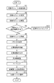
図2は、本実施形態の圧電デバイス10の製造工程のフローチャート図である。
Next, a method for manufacturing the
FIG. 2 is a flowchart of the manufacturing process of the
ステップS1では、基板31に各回路素子50a〜50fをSMT(Surface Mount Technology)によって実装し、回路モジュール30を製造する。回路モジュール30の製造は、まず、基板35のパターン電極32a〜32lに、スクリーン印刷法によって半田ペーストを所定量塗布する。次に、対をなすパターン電極32aと32b,32cと32d,32eと32f,32gと32h,32iと32j,32kと32lの、それぞれに対応する回路素子50a〜50fを、チップマウンタ等を用いて所定位置に位置決めする仮搭載を行なう。次に、各回路素子50a〜50fが仮搭載された基板35を、リフロー炉等によって半田溶融温度等を考慮した温度プロファイルにて加熱することにより、半田を溶解させて回路素子50a〜50fを接合させる。そして、有機溶剤等からなる洗浄液によって回路モジュール30を洗浄し、半田ペーストに含有されたフラックスや、半田リフローによって発生する半田ボール等を除去する(ステップS2)。
In step S1, each
ステップS3では、回路モジュール30の検査を行なう。検査は、外観検査、電気特性検査などの方法により、各回路素子50a〜50fが適正に接合されているか否かを判定する(ステップS4)。回路素子の接合不良が発見された場合(ステップS4でNo)には、当該箇所の修正を行ない(ステップS13)、ステップS2の回路モジュール洗浄工程に再投入される。なお、ステップS4で発見された不良箇所が修正不可能な状態となった場合には、不良品として分別される。
In step S3, the
回路モジュール30の検査にて、回路素子50a〜50fが適正に接合されていると判定された場合(ステップS4でYes)には、ステップS5に進んで、パッケージ本体1に回路モジュール30を搭載する。まず、パッケージ本体1のマウント電極3a,3bに、ディスペンサ等によって半田ペーストを所定量塗布し、次に、回路モジュール30の外部接続端子33a,33bを、それぞれ対応するパッケージ本体1のマウント電極3a,3b上に位置決めして仮搭載する。次に、リフロー炉等によりパッケージ本体1を加熱して半田接合をおこない、回路モジュール30の搭載を完了させる。そして、有機溶剤等からなる洗浄液によって、回路モジュール30が搭載されたパッケージ本体を洗浄して、フラックス等の汚染物質や付着物を除去する(ステップS6)。
When it is determined in the inspection of the
ステップS7では、パッケージ本体1のマウント電極4a,4b上に所定量の導電性接着剤120を塗布し、圧電振動片20の接続電極を、それぞれ対応するマウント電極4a,4bに位置決めして圧電振動片20が略水平になるように仮搭載し、導電性接着剤120を乾燥させることによって圧電振動片20を固定して搭載を完了させる。
In step S7, a predetermined amount of
ステップS8では、純水等により、圧電振動片20の清浄化を目的とする洗浄を行なう。次に、パッケージ本体1を介して回路モジュール30と電気的に接続された圧電振動片20の周波数を、所望の値に調整する周波数調整をおこなう(ステップS9)。
In step S8, cleaning for the purpose of cleaning the piezoelectric vibrating
ステップS10では、圧電振動片20及び回路モジュール30が搭載されたパッケージ本体1を、所定温度の乾燥炉に所定時間入れて乾燥させるベーキングを行なう。続いて、ステップS11では、パッケージ本体1の上面に、シールリング9を介して金属製のパッケージ蓋体2を接合し、パッケージ本体1の内部の気密が保たれれるように封止して、圧電デバイス10を得る。
In step S10, baking is performed in which the
ステップS12では、圧電デバイス10の電気的特性が所定の範囲内にあるか否かを確認する電気特性検査を行い、圧電デバイス10の一連の製造工程を終了する。
In step S12, an electrical property test is performed to confirm whether or not the electrical property of the
次に、上記実施形態の効果を以下に記載する。 Next, the effect of the said embodiment is described below.
(1)上記実施形態では、圧電振動片20とともに圧電デバイス10のパッケージ本体1の凹底部に搭載する複数の回路素子50a〜50fを、まず、基板35に接合させて回路モジュール30を得た。そして、回路モジュール30を、パッケージ本体1の凹底部のマウント電極3a,3bに接合する構成とした。
(1) In the above embodiment, the
この構成によれば、従来の、パッケージ本体1の凹底部に直接回路素子50a〜50fを搭載する方式の場合に、パッケージ本体1の側壁部分1aが障害物となって困難であった側壁部分1a近傍への各種回路素子の配置が可能となる。この結果、省スペースにて回路素子50a〜50fをパッケージ本体1の凹底部に搭載することができるので、圧電デバイス10の、特に平面方向の小型化を図ることが可能となる。
また、回路モジュール30は、基板35の回路配線設計により汎用性を持たせることも可能であるため、別機種の圧電デバイスに用いることも可能となり、圧電デバイス製造の低コスト化や、新規圧電デバイスの量産化における納期短縮等に寄与することが可能となる。
According to this configuration, in the case of the conventional system in which the
Further, since the
(2)上記実施形態では、基板35に各回路素子50a〜50fを接合するときに、SMTにより実装方式を採用した。
この結果、例えば、多数個取りの基板を用いて、半田ペーストの塗布にはスクリーン印刷法が適用できるので、効率的かつ高品質な回路素子実装が可能となり、圧電デバイス10の効率的な製造と低コスト化に寄与することが可能となる。また、回路モジュール30は、各回路素子50a〜50fが半田により接合されているので、検査工程にて半田付け不良があった場合に、修正して良品とすることも可能である。
(2) In the above embodiment, when the
As a result, for example, a screen printing method can be applied to the application of the solder paste using a multi-piece substrate, so that efficient and high-quality circuit element mounting can be achieved, and the
(3)上記実施形態では、基板35に各回路素子50a〜50fを実装した回路モジュール30を、洗浄液でフラックス洗浄してから、パッケージ本体1に搭載する構成とした。この結果、従来のパッケージ本体1の凹底部に各回路素子50a〜50fを実装する場合に、該凹底部にフラックス残渣が発生し易いという問題が解消でき、高い洗浄性を確保できるので、フラックス残渣による基板35の回路配線のマイグレーション等を抑制することが可能となる。また、フラックス残渣が圧電振動片20に付着して機能不良を引き起こすことも抑制できる。従って、高信頼性を有する圧電デバイス10を得ることが可能となる。
(3) In the above embodiment, the
(第2の実施形態)
上記第1の実施形態では、複数の回路素子50a〜50fが実装された回路モジュール30を、そのままパッケージ本体1に搭載する構造の圧電デバイス10について説明したが、これに限定されない。回路モジュールに実装された複数の回路素子及び基板との接合部分を樹脂封止して、パッケージ本体1に搭載する構成としてもよい。
(Second Embodiment)
In the first embodiment, the
図3(a)は、樹脂封止された回路モジュールが搭載された圧電デバイスの構造を説明するための正面図、同図(b)は、その圧電デバイスの図3(a)中のA−A断面図、図4は、本第2の実施形態の圧電デバイス60の製造工程のフローチャート図である。なお、本第2の実施形態の圧電デバイス60の構成のうち、上述した第1の実施形態と同様の構成については同一符号を用いて説明し、同一の構成については説明を省略する。
図3(a)において、圧電デバイス60は、圧電振動片20と、樹脂封止型回路モジュール70とが、パッケージ本体1の凹底部に電気的に接続されながら搭載され、パッケージ本体1の上面開口がパッケージ蓋体2により封止された構成を有している。
FIG. 3A is a front view for explaining the structure of a piezoelectric device on which a resin-sealed circuit module is mounted, and FIG. 3B is a cross-sectional view of the piezoelectric device shown in FIG. A sectional view and FIG. 4 are flowcharts of the manufacturing process of the
In FIG. 3A, the
樹脂封止型回路モジュール70は、基板35のメインパターン形成面31aに形成された複数の対をなすパターン電極32a〜32lに、それぞれに対応する回路素子50a〜50fが半田接合により接合され、封止樹脂100で樹脂封止されている。基板35の裏面31bには外部接続端子33a,33bが形成され、メインパターン形成面31aの配線パターンと図示しない導通性を有したスルーホールによって導通している。そして、樹脂封止型回路モジュール70は、パッケージ本体1の凹底部に形成されたマウント電極3a,3bと、それぞれに対応する外部接続端子33a,33bを位置決めして、半田によって接合されている。
In the resin-sealed
次に、上記の圧電デバイス60を製造する方法について、図面に従って説明する。
ステップS21では、基板35に、各回路素子50a〜50fをSMTにより実装して回路モジュールを製造する。
ステップS22では、有機溶剤等からなる洗浄液によって回路モジュールを洗浄し、フラックスや、半田リフローによって発生する半田ボール等を除去する。
Next, a method for manufacturing the
In step S21, each
In step S22, the circuit module is cleaned with a cleaning liquid made of an organic solvent or the like to remove flux, solder balls generated by solder reflow, and the like.
ステップS23では、回路モジュールを、キャビティが形成された上下の樹脂封止金型で挟み込み、封止樹脂100をキャビティに注入して充填させるトランスファモールド法によって樹脂封止し、樹脂封止型回路モジュール70を製造する。なお、樹脂封止方法はトランスファモールド法に限らず、例えばディスペンサで封止樹脂100を吐出させて塗布するポッティング法等、他の樹脂封止方法を用いてもよい。
In step S23, the circuit module is sandwiched between upper and lower resin-sealed molds in which cavities are formed, and resin-sealed by a transfer mold method in which the sealing
ステップS24では、樹脂封止型回路モジュール70の検査を行なう。検査は、封止樹脂の未充填等の外観的な良否を判定する外観検査と、回路モジュールの電気特性の良否を判定する電気特性検査方法があり、このうち少なくとも一方を行なう。検査にて不良と判定された場合(ステップS25でNo)には、不良品として分別される(ステップS34)。
In step S24, the resin-sealed
樹脂封止型回路モジュール70の検査にて、良品と判定された場合(ステップS25でYes)には、ステップS26に進んで、パッケージ本体1のマウント電極3a,3bに、それぞれ対応する樹脂封止型回路モジュール70の外部接続端子33a,33bを位置合わせして半田接合することに、樹脂封止型回路モジュール70が搭載される。次に、有機溶剤等からなる洗浄液によって洗浄し、フラックス等を除去する(ステップS27)。
If it is determined that the product is non-defective in the inspection of the resin-sealed circuit module 70 (Yes in Step S25), the process proceeds to Step S26, and the resin sealing corresponding to the
ステップS28では、パッケージ本体1のマウント電極4a,4bと、それぞれ対応する圧電振動片20の接続電極とを位置決めして、導電性接着剤により接合し、圧電振動片20を搭載させる。
In step S28, the
ステップS29では、純水等により圧電振動片20の洗浄を行ない、次に、圧電振動片20の周波数調整をおこなう(ステップS30)。そして、圧電振動片20及び樹脂封止型回路モジュール70が搭載されたパッケージ本体1を、所定温度の乾燥炉に所定時間入れてベーキングを行なう(ステップS31)。
In step S29, the piezoelectric vibrating
続いて、ステップS32では、パッケージ本体1の上面に、シールリング9を介してパッケージ蓋体2を接合して圧電デバイス60を得る。最後に、圧電デバイス60の電気特性検査を行い(ステップS33)、一連の製造工程を終了する。
Subsequently, in step S <b> 32, the
この構成によれば、樹脂封止型回路モジュール70は、搭載されている各回路素子50a〜50f、及び各回路素子50a〜50fと基板35との接合部分が封止樹脂100によって封止されている。これにより、例えば基板35に各回路素子50a〜50fをSMTにより実装する際に発生する半田ボールや半田屑などの導電性を有した異物が、回路モジュール洗浄工程(図4のステップS22)で除去しきれずに残留した場合等に、該導電性を有する異物が、圧電振動片20やその接続部分に付着して、圧電振動片20の振動特性への悪影響や、電気的な短絡等の悪影響を及ぼす危険を回避することができる。また、基板35や各回路素子50a〜50f、及びSMTにより実装した際のフラックス等の残留物等のアウトガスが発生して圧電振動片20付着し、振動特性等に悪影響を及ぼす等の不具合を回避することが可能となる。従って、圧電振動片20による振動特性に優れ、高信頼性を有する圧電デバイス60を提供することが可能となる。
According to this configuration, the resin-sealed
本発明は、前記各実施形態に限定されるものではなく、以下の変形例を実施することもできる。 The present invention is not limited to the above-described embodiments, and the following modifications can also be implemented.
(変形例1) 上記第1及び第2の実施形態では、パッケージ本体1の凹底部に設けられたマウント電極3a,3bに、回路モジュール30または樹脂封止型回路モジュール70を接続する際に、半田によって接合する方法を示したが、これに限定されない。例えば、導電性接着材を用いて、パッケージ本体1aのマウント電極3a,3bに回路モジュール30を接合する等、他の接合方法を用いる構成としてもよい。
この構成によれば、半田ペーストを使用しないので、回路モジュール30または樹脂封止型回路モジュール70を搭載した後にフラックス洗浄をする必要がなくなり、製造工程を減らすことができる。
(Modification 1) In the first and second embodiments, when the
According to this configuration, since no solder paste is used, it is not necessary to perform flux cleaning after mounting the
(変形例2)上記第1及び第2の実施形態では、基板35に各回路素子50a〜50fを、半田によるSMTによって接合する構成としたが、これに限らない。導電性接着剤を用いたり、ACF(Anisotropic Conductive Film)等の電気的接合材料を使って接合するなどの、他の接合方式を用いてもよい。
(Modification 2) In the first and second embodiments, the
1…パッケージ本体、2…蓋体としてのパッケージ蓋体、3a,3b…パッケージ本体の凹底部に設けられた電極であるマウント電極、4a,4b…圧電振動片が接合される電極であるマウント電極、10,60…圧電デバイスである圧電デバイス、32a〜32l…基板の電極であるパターン電極、35…基板、50a〜50f…電子部品としての回路素子、100…基板に接合された電子部品の樹脂封止に用いる封止樹脂。
DESCRIPTION OF
Claims (2)
圧電振動片と、複数の電子部品と、前記パッケージ本体の凹部内を気密に封止する蓋体と、を備え、
前記圧電振動片及び前記電子部品が、前記パッケージ本体の複数の電極に接合されている構造の圧電デバイスであって、
前記電子部品は基板に接合され、該基板が、前記複数の電極のうちのいずれかに接合されていることを特徴とする圧電デバイス。 A package body having a plurality of electrodes provided on the bottom plane of the recess, wherein a recess is formed;
A piezoelectric vibrating piece, a plurality of electronic components, and a lid for hermetically sealing the inside of the recess of the package body,
A piezoelectric device having a structure in which the piezoelectric vibrating piece and the electronic component are joined to a plurality of electrodes of the package body,
The electronic device is bonded to a substrate, and the substrate is bonded to any one of the plurality of electrodes.
前記基板に接合された電子部品が樹脂封止されていることを特徴とする圧電デバイス。
The piezoelectric device according to claim 1.
An electronic component bonded to the substrate is sealed with a resin.
Priority Applications (1)
| Application Number | Priority Date | Filing Date | Title |
|---|---|---|---|
| JP2005242243A JP2007060214A (en) | 2005-08-24 | 2005-08-24 | Piezoelectric device |
Applications Claiming Priority (1)
| Application Number | Priority Date | Filing Date | Title |
|---|---|---|---|
| JP2005242243A JP2007060214A (en) | 2005-08-24 | 2005-08-24 | Piezoelectric device |
Publications (2)
| Publication Number | Publication Date |
|---|---|
| JP2007060214A true JP2007060214A (en) | 2007-03-08 |
| JP2007060214A5 JP2007060214A5 (en) | 2008-09-25 |
Family
ID=37923309
Family Applications (1)
| Application Number | Title | Priority Date | Filing Date |
|---|---|---|---|
| JP2005242243A Withdrawn JP2007060214A (en) | 2005-08-24 | 2005-08-24 | Piezoelectric device |
Country Status (1)
| Country | Link |
|---|---|
| JP (1) | JP2007060214A (en) |
-
2005
- 2005-08-24 JP JP2005242243A patent/JP2007060214A/en not_active Withdrawn
Similar Documents
| Publication | Publication Date | Title |
|---|---|---|
| US7456552B2 (en) | Piezo-electric oscillator and method of manufacturing the same | |
| US7551040B2 (en) | Surface mount crystal oscillator | |
| JP2001196488A (en) | Electronic component device and manufacturing method thereof | |
| US20110193645A1 (en) | Piezoelectric vibrator and oscillator using the same | |
| US8072276B2 (en) | Surface mount crystal oscillator | |
| JP4091868B2 (en) | Surface mount temperature compensated crystal oscillator | |
| JP2005244639A (en) | Temperature compensated crystal oscillator | |
| JP4508041B2 (en) | Piezoelectric device | |
| JP2005065104A (en) | Surface mounted piezoelectric vibrator and its manufacturing method | |
| JP2007060214A (en) | Piezoelectric device | |
| JP2000244090A (en) | Structure of electronic component and its support structure | |
| JP2007088979A (en) | Piezoelectric device | |
| JP4284143B2 (en) | Piezoelectric oscillator | |
| JP2015195593A (en) | crystal oscillator | |
| JP5942312B2 (en) | Assembling method of crystal oscillator | |
| JP2004260598A (en) | Surface mount temperature compensation crystal oscillator | |
| JP2005109576A (en) | Piezoelectric oscillator | |
| JP2009302996A (en) | Method of manufacturing piezoelectric device | |
| JP2000315918A (en) | Crystal oscillator | |
| JPH118334A (en) | Intermediate of ball grid array package and its manufacture | |
| JP4284142B2 (en) | Piezoelectric oscillator | |
| JP2008187751A (en) | Surface mount piezoelectric oscillator | |
| JP2008010922A (en) | Piezoelectric oscillator | |
| JP2005039791A (en) | Temperature compensated crystal oscillator | |
| JP2007067832A (en) | Piezoelectric oscillator and manufacturing method thereof |
Legal Events
| Date | Code | Title | Description |
|---|---|---|---|
| RD04 | Notification of resignation of power of attorney |
Free format text: JAPANESE INTERMEDIATE CODE: A7424 Effective date: 20070405 |
|
| A521 | Request for written amendment filed |
Free format text: JAPANESE INTERMEDIATE CODE: A523 Effective date: 20080811 |
|
| A621 | Written request for application examination |
Free format text: JAPANESE INTERMEDIATE CODE: A621 Effective date: 20080811 |
|
| A977 | Report on retrieval |
Free format text: JAPANESE INTERMEDIATE CODE: A971007 Effective date: 20100108 |
|
| A131 | Notification of reasons for refusal |
Free format text: JAPANESE INTERMEDIATE CODE: A131 Effective date: 20100119 |
|
| A761 | Written withdrawal of application |
Free format text: JAPANESE INTERMEDIATE CODE: A761 Effective date: 20100316 |