JP2007017444A - Test socket - Google Patents
Test socket Download PDFInfo
- Publication number
- JP2007017444A JP2007017444A JP2006189459A JP2006189459A JP2007017444A JP 2007017444 A JP2007017444 A JP 2007017444A JP 2006189459 A JP2006189459 A JP 2006189459A JP 2006189459 A JP2006189459 A JP 2006189459A JP 2007017444 A JP2007017444 A JP 2007017444A
- Authority
- JP
- Japan
- Prior art keywords
- contact
- housing
- test socket
- lid
- slot
- Prior art date
- Legal status (The legal status is an assumption and is not a legal conclusion. Google has not performed a legal analysis and makes no representation as to the accuracy of the status listed.)
- Granted
Links
Images
Classifications
-
- G—PHYSICS
- G01—MEASURING; TESTING
- G01R—MEASURING ELECTRIC VARIABLES; MEASURING MAGNETIC VARIABLES
- G01R31/00—Arrangements for testing electric properties; Arrangements for locating electric faults; Arrangements for electrical testing characterised by what is being tested not provided for elsewhere
- G01R31/26—Testing of individual semiconductor devices
-
- G—PHYSICS
- G01—MEASURING; TESTING
- G01R—MEASURING ELECTRIC VARIABLES; MEASURING MAGNETIC VARIABLES
- G01R1/00—Details of instruments or arrangements of the types included in groups G01R5/00 - G01R13/00 and G01R31/00
- G01R1/02—General constructional details
- G01R1/04—Housings; Supporting members; Arrangements of terminals
- G01R1/0408—Test fixtures or contact fields; Connectors or connecting adaptors; Test clips; Test sockets
- G01R1/0433—Sockets for IC's or transistors
- G01R1/0441—Details
- G01R1/0466—Details concerning contact pieces or mechanical details, e.g. hinges or cams; Shielding
-
- H10P74/00—
Landscapes
- Physics & Mathematics (AREA)
- General Physics & Mathematics (AREA)
- Engineering & Computer Science (AREA)
- Computer Hardware Design (AREA)
- Microelectronics & Electronic Packaging (AREA)
- Testing Of Individual Semiconductor Devices (AREA)
- Coupling Device And Connection With Printed Circuit (AREA)
- Connecting Device With Holders (AREA)
Abstract
【課題】 集積回路のテストで用いるための改良型テストソケット。
【解決手段】 このテストソケットは、内部に形成された1つ以上のスロットを有するハウジングを含む。接点は各スロット内で受け入れられ、ロドボド上のトレスと嵌合する接点の後端とともに内部で維持される。設置はエラストマ組手段により達成され、接点の前端がテスト対象装置のリドまたはパッドにより嵌合され、その対応スロット内に押し込まれると、各接点の後端における弓状面が、事実上非並進または回転滑動しながらその対応トレスで回転するよう、エラストマが各接点を維持する。
【選択図】 図1An improved test socket for use in integrated circuit testing.
The test socket includes a housing having one or more slots formed therein. A contact is received within each slot and is maintained internally with the back end of the contact mating with the tres on the rhodobo. Installation is accomplished by means of an elastomer assembly, and when the front end of the contact is fitted by the lid or pad of the device under test and pushed into its corresponding slot, the arcuate surface at the rear end of each contact is effectively non-translated or The elastomer maintains each contact so that it rotates with its corresponding tress while sliding.
[Selection] Figure 1
Description
本発明は電子部品テスト技術に関する。しかしながら、さらに詳細には、本発明は、電子部品をテストするための接点を用いるテストソケットに関する。テストソケットは、テスト対象の電子部品のリドあるいはパッドと、ロドボド上の対応するトレスとの間に電子経路を相互結合し、それをもたらす接点を含む。本発明は、テストソケットの対応接点により装置のリドあるいはパッドおよびロドボドにかかる力の制御および調整に焦点を合わせる。 The present invention relates to an electronic component test technique. More particularly, however, the invention relates to a test socket that uses contacts for testing electronic components. The test socket includes contacts that interconnect and provide an electronic path between the lid or pad of the electronic component to be tested and the corresponding tres on the rhodobo. The present invention focuses on the control and adjustment of the force applied to the device lid or pad and rodbode by corresponding contacts on the test socket.
集積回路装置のテストは、電子装置に対して可能な限り高度な品質管理を得るため、長年にわたって遵守された手順である。テスタは、典型的には、テスタ装置と関連するロドボド上に形成された複数の導電性トレスを含む。テストを実施するため、導通装置の導線、あるいは非導電装置のパッドを、ロドボド上の対応トレスに相互接続する必要がある。複数接点を備えたテストソケットは、相互接続を実施するため、テスト対象装置とロドボドとの間に介装される。1つの接点は、前端において、テスト対象装置の導線またはパッドを、ロボド上の対応トレスと嵌合する。 Integrated circuit device testing is a procedure that has been followed for many years in order to obtain the highest possible quality control for electronic devices. The tester typically includes a plurality of conductive tresses formed on a rhodobo associated with the tester device. In order to perform the test, the conducting device leads or non-conducting device pads need to be interconnected to corresponding troughs on the rhodobo. A test socket with a plurality of contacts is interposed between the device under test and Rhodobod to perform interconnection. One contact, at the front end, mates the lead or pad of the device under test with a corresponding trace on the robot.
長年にわたり、このような接点の形状および構成は、テストソケットの構成、ロドボド、テスト対象装置の構造に応じて発展してきた。以前は、良好な伝送経路をもたらすため、接触端部における嵌合の種々な位置でぬぐい作業を行なうことが必要と考えられていた。しかしながら、技術の進歩につれて、以前考えられていたより少ないぬぐい作業でも良好な伝送経路を維持することが必要であることが明白になってきた。さらに、過剰なぬぐい作業により嵌合のさまざまなポイントで構成部品に損傷をもたらし、テストソケットやテスタロドボドの寿命を顕著に縮めることが明らかとなった。従って、面対面の摩滅を最小限にするため、さまざまな試みがなされている。しかしながら、現在の最先端の技術では、テストソケットの効率を最大化するとともに、磨耗やそれに続く構成部品の劣化を最小化することの両方に対して適した構成を決めることができなかった。 Over the years, the shape and configuration of such contacts has evolved depending on the configuration of the test socket, the rhodobo, and the structure of the device under test. Previously, it was considered necessary to perform wiping work at various positions of the fitting at the contact end to provide a good transmission path. However, as technology has advanced it has become clear that it is necessary to maintain a good transmission path with less wiping work than previously thought. Furthermore, it has been found that excessive wiping operations can cause damage to components at various points of mating and significantly shorten the life of test sockets and testarodbods. Accordingly, various attempts have been made to minimize face-to-face wear. However, current state-of-the-art technology has failed to determine a suitable configuration for both maximizing test socket efficiency and minimizing wear and subsequent component degradation.
本発明が目指すものは、従来技術のそのような問題点や指示に関する。本発明の利点は、発明の概要、発明の詳細な説明、付録請求項、添付図面を参照することでさらに明白になる。 The aim of the present invention relates to such problems and instructions of the prior art. The advantages of the present invention will become more apparent by referring to the summary of the invention, the detailed description of the invention, the appended claims, and the accompanying drawings.
本発明は改良型テストソケットである。これは、テスタロドボド面と嵌合する場所である第1面を備えたハウジングを含む。このハウジングは、ハウジングの第1面とほぼ平行で、それと離間した第2面を備えた。ハウジングの第2面は、第1面が対面する方向と反対に対面する。少なくとも1つのスロットは、その第1面と第2面との間のハウジングを通して延伸し、ハウジング内で形成される。接点は対応スロットで受け入れられる。このような接点は、テスト対象装置の対応リドあるいはパッドにより嵌合されるハウジングの第2面を突き抜けて垂直に延伸する前端を備えた。接点はさらに、弓状面を規定する後端をもち、この弓状面は、テスタロドボド面に形成された対応トレスを嵌合する。この接点は、接点の前端がテスト対象装置のリドまたはパッドにより嵌合され、そのスロットに押し込まれると、接点の弓状面が、事実上非並進あるいは回転滑動しながらテスタロドボド面の対応トレスにわたって回転するようスロット内に弾性的に設けられる。これにより、接点とロドボドとの間の磨耗が実質的になくなる。 The present invention is an improved test socket. This includes a housing with a first surface that is where it mates with the testarodbod surface. The housing had a second surface substantially parallel to and spaced from the first surface of the housing. The second surface of the housing faces opposite to the direction in which the first surface faces. At least one slot extends through the housing between its first and second surfaces and is formed within the housing. Contacts are received in corresponding slots. Such a contact has a front end that extends vertically through the second surface of the housing fitted by a corresponding lid or pad of the device under test. The contact further has a rear end that defines an arcuate surface that engages a corresponding trace formed on the testarodbod surface. This contact is fitted over the corresponding trestle of the Testarodbo surface when the front end of the contact is fitted by the lid or pad of the device under test and pushed into its slot, causing the arcuate surface of the contact to move virtually non-translating or rotationally sliding. Elastically provided in the slot. This substantially eliminates wear between the contacts and the rhodobodo.
接点の後端は、ロドボドとの嵌合で弓状面を規定することに加えて、その弓状面から角度離間し、徐々に弓状になった面も規定する。この実施例において、ハウジングはスロット内の壁を規定する。この壁は接点の後端の徐々に弓状になった面で嵌合され、徐々に弓状になった面と壁との間の空間関係は、接点の前端がテスト対象装置のリドまたはパッドにより嵌合され、対応スロットに押し込まれると、徐々に弓状になった面が壁に沿って動き、接点の弓状面をその対応トレスにわたって回転させる。ハウジングにより規定される壁が、ハウジングの第1面に対して鋭角で角度離間することが予測される。これにより、接点の弓状面が事実上非並進あるいは回転滑動しながらテスタロドボドのトレスにわたって回転できるようになる。 In addition to defining an arcuate surface by mating with the rhodobod, the rear end of the contact also defines an arcuate surface that is angularly spaced from the arcuate surface. In this embodiment, the housing defines a wall within the slot. This wall is fitted with a gradually arcuate surface at the rear end of the contact, and the spatial relationship between the gradually arcuate surface and the wall is such that the front end of the contact is the lid or pad of the device under test. And is pushed into the corresponding slot, the arcuate surface gradually moves along the wall and rotates the arcuate surface of the contact across its corresponding trace. It is anticipated that the walls defined by the housing will be angularly spaced apart at an acute angle with respect to the first surface of the housing. This allows the arcuate surfaces of the contacts to rotate across the tester throat tress while virtually non-translating or rotationally sliding.
本発明はこれにより、従来技術の指示を扱い、その問題を解決する改良型テストソケットである。これらの機能の観点から得られるさらに詳細な機能や利点は、発明の詳細な説明、請求項、添付図面を参照することでさらに明白になる。 The present invention thereby provides an improved test socket that handles prior art instructions and solves the problem. More detailed features and advantages obtained in view of these features will become more apparent with reference to the detailed description of the invention, the claims and the accompanying drawings.
本発明の好ましい実施例では、接点の弾性取付けを行うため、スロットに対して直交するエラストマ対を用いる。前エラストマは、テスタロドボド面と接点との間のチャネル内に置かれる。前エラストマは、ハウジングにより規定されたショルダが接点を嵌合し、ハウジングの第2面を越えて延伸する距離を制限するために用いることができることから、あらかじめ圧縮される。これにより、あらかじめ圧縮する作業は、前エラストマを間に挟む接点とロドボドとで達成される。前エラストマは、テスト対象装置のリドまたはパッドにより嵌合され、そのそれぞれのスロットに押し込まれると接点によりさらに圧縮される。 The preferred embodiment of the present invention uses an elastomer pair orthogonal to the slot to provide resilient attachment of the contacts. The pre-elastomer is placed in the channel between the testarodot surface and the contact. The front elastomer is pre-compressed because the shoulder defined by the housing can be used to fit the contacts and limit the distance that it extends beyond the second surface of the housing. As a result, the pre-compression operation is achieved by the contact point and the rhodobo that sandwich the front elastomer. The front elastomer is fitted by the lid or pad of the device under test and is further compressed by the contacts when pushed into its respective slot.
後エラストマは、接点の後端に予圧をかける。これにより、テスタロドボド面上の対応トレスに対する各接点の後端の間に接点を維持する。
本発明は貴金属製接点として用いることができる。このような接点はロドボド寿命を延ばす。NeyoroG接点は、めっきのない固体金合金製接点である。このような材料により接点の寿命が延びることが見出された一方、同様にロドボドの寿命も延びる。接点に対してNeyoroG材料を用いることで、ロドボドの寿命が、従来技術により公知のメカニズムでのロドボドの寿命より少なくとも2倍にできることがわかった。
The rear elastomer preloads the rear end of the contact. This maintains a contact between the rear ends of each contact relative to the corresponding trace on the testarodbo surface.
The present invention can be used as a noble metal contact. Such contacts extend the rhodobo life. The NeyoroG contact is a solid gold alloy contact without plating. While it has been found that such materials extend the life of the contacts, the life of the rhodobo is also increased. It has been found that the use of a NeyoroG material for the contacts can at least double the lifetime of rhodobod with that known in the prior art.
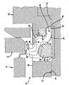
ここで図面を参照するが、この中で同様の参照番号は複数図を通して同様の要素を表しており、図1は本発明によるテストソケット10を示す。テストソケット10は、電子器具で用いられる集積回路の品質を確認するため、典型的に用いられるテスタとともに利用することが意図されている。テスタは、テスタと試験対象の集積回路装置18との間の電子通信を可能にするため、表面16上に形成された電導性トレス14を備えたテスタロドボド12との間でインタフェイスを取る。すなわち、電気信号がテスト対象装置18とテスト装置との間でテストソケット10を通して伝送される。
Reference is now made to the drawings, wherein like reference numerals represent like elements throughout the several views, and FIG. 1 illustrates a
図1は、複数のリド20とともに提供されるDUTパッケジを示すが、それらリドのうちの1つだけが示されている。図1は、テスト対象装置18の一部だけを示しているが、実質的に同一のリドは装置パッケジ18の反対側の両方に沿って延伸することが理解される。
FIG. 1 shows a DUT package provided with a plurality of lids 20, but only one of the lids is shown. Although FIG. 1 shows only a portion of the device under
図1は、テスト対象装置18がテストソケット10の対応接点24と接するリド20と嵌合する場合、リド20の曲げを防止するリド裏地をさらに示す。下向きの圧力が(図示されていない)プランジ機構によりテスト対象装置18にかけられる。プランジャは、テスト実施時、弾性取り付けされた接点24によりかけられる上向きバイアスより大きくな
るよう、接点24を押し下げる。図1は、テスト対象装置18が接点24と嵌合する前の接点24の正常位置を示す。同図ではさらに、プランジャがテスト対象装置をテスト位置まで押し下げた場合の接点位置をファントムで示す。典型的には、プランジャが移動する軸に沿った接点24の前端26の移動距離は0.3ミリメトルの状態である。以下で論じるとおり接点24の構成に関して、下縁の接点24の後端30における弓状面28は、トレス14に沿った面の実施的に非並進あるいは回転滑動なくロドボド12上の対応トレス14で回転することが理解される。最適な方法として、トレス14にかかる衝撃を制限するため、弓状面28ができるだけ大きな曲率半径を備えたようにする。さらに、接点24の構成から、接点が対応テスト対象装置18のリド20に沿った接点24の前端の並進滑動は、接点の前端をかなり洗浄する際には適しているが、装置18のリド20上での洗浄は最小であることがわかった。例えば、本発明の1つの実施例において、並進滑動は装置18上で0.041ミリメートルの状態である。
FIG. 1 further illustrates a lid lining that prevents bending of the lid 20 when the device under
テストソケット10は、トレス14が形成されるテスタロドボド12の面16とほぼ嵌合する第1面34を備えたハウジング32を含む。このハウジング32は、ハウジングの第1面とほぼ平行で、それと離間した第2面36を備えた。ハウジング32の第2面36は第1面34の反対側に対面する。前に論じたとおり、ハウジング32は複数の接点24をもつ。複数のスロット38が設けられるが、各スロットは接点24のうちの1つだけを受け入れる。
The
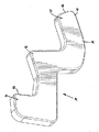
図2は、本発明による個々の接点を透視図で示す。接点24は、第1、第2、第3の突出40,42,44を含む。第1突出40は、ロドボド12のトレス14を嵌合する接点24の後端30で規定される。第3突出44は、テスト対象装置18のリド20またはパッドで嵌合される接点24の前端26により規定される。第2突出42は、以下で論じるとおり複数エラストマ46,48で設けられる場合、ハウジング32で規定されるショルダ49を嵌合するよう機能する。第2突出42によるショルダ49の嵌合は、接点49の上方への移動の程度を制限するよう機能し、接点24がテスト対象装置により嵌合されない場合、接点24の前端26の距離はハウジング32の第2面36を越えて延びる。
FIG. 2 shows the individual contacts according to the invention in a perspective view. The
再び図1を参照すると、テストソケット10は、ハウジング32内に形成されたスロット38で規定される面をほぼ横断する軸に沿って延伸するチャネル50,52対を有する。これらのチャネル50,52は、接点24をスロット38に設けるよう機能するエラストマ46,48を受け入れるよう意図されたものである。図1は、大きい前エラストマ46を受けいれるほぼ円形のチャネル50と、小さい後部エラストマ48を受け入れる角形のチャネル52とを示す。後エラストマ48は予圧されるが、その理由は、ロドボド12と勘合している接点29の後端30の弓状面28が、接点24の前端26を上に押し上げるような位置で接点24の後端30の上縁を嵌合するためである。同様に、前エラストマ46も圧縮され、さらに接点24を上方に押し上げ、テスト対象集積回路装置18のリド24またはパッドにより最初の接点のポイントに向けてバイアスをかけるよう機能する。
Referring again to FIG. 1, the
前に述べたとおり、ロドボド12上のトレス14と嵌合する弓状面28は、ロドボド12のトレス14に沿って、あったとしても、適切な並進あるいは回転滑動ではない。この理由は、スロット38の端部近くの第1面34に近いハウジング32内で規定される角度のついた壁54があるためである。接点24の後端30は、弓状面28を規定することに加えて、ハウジング32で規定される角度のついた壁54を嵌合する接点24の後端30の縁部で徐々に弓状になった面56も有する。接点24の配置は、弓状面28の接点がロドボドトレス14にわたって動きながらも、そのトレス14にわたって滑動しないよう、スロット38の端部で規定される角度のついた壁54と相互作用するものとなる。この動きは事実上すべて回転アクション(すなわち、トレスにわたる相対移動が滑動なく表面上の車輪回転となるもの)である。これは徐々に弓状になる面56により生じるものである
が、その理由は、徐々に弓状になる面56の嵌合が角度のついた壁54との接触を維持するため、接点24の後端30の弓状面28が並進滑動することなく回転できるようにする輪郭を有するためである。テスト対象装置18が引き出されると、逆方向での回転が起こる。
As previously mentioned, the arcuate surface 28 that mates with the tres 14 on the
前で論じたとおり、装置の引き出しが行われると、接点24の上方への動きを制限するため、第2突出42が、ハウジング32で規定されたショルダ49を嵌合する。
また、テスト対象装置18による力の作用点は、接点24の後端30とロドボド12上のトレス14との嵌合点から比較的大きな距離で離間している点が指摘される。これにより、ロリング作用(すなわち、ロドボドへの損傷等の最小化)により達成される利点が大きくなる。
As discussed above, when the device is withdrawn, the second protrusion 42 engages a shoulder 49 defined by the
Further, it is pointed out that the point of action of the force by the
さらに、貴金属製接点を本発明で使うこともできる。このような接点はロドボド寿命も延ばす。めっきをもたない固体金合金製接点であるNeyoroG接点の利用が考えられる。この材料は接点の寿命を延ばすだけでないことがわかった。この材料はまた、トレスに対する損傷を最小限にすることでロドボドの寿命も延ばす。ロドボドの寿命は従来技術で知られるもので構成された機構では、少なくとも二倍になることがわかった。 In addition, noble metal contacts can be used in the present invention. Such contacts also extend the rhodobo life. It is conceivable to use a Neyoro G contact, which is a solid gold alloy contact having no plating. This material has been found to not only extend the life of the contacts. This material also extends the life of the rhodobo by minimizing damage to the tres. Rhodobo's lifetime has been found to be at least doubled with mechanisms constructed from what is known in the prior art.
この開示は、多くの点で、明示的なものでだけであることが理解される。本発明の適用範囲を逸脱することなく、詳細、特に形状、寸法、材料、部品配置に関して変更を行ってもよい。したがって、本発明の適用範囲は添付請求項の文言で定義されるとおりである。 It is understood that this disclosure is in many respects only explicit. Changes may be made in details, particularly in terms of shape, dimensions, materials and component placement, without departing from the scope of the invention. Accordingly, the scope of the present invention is as defined in the language of the appended claims.
Claims (8)
対応するスロットで受け入れられ、テスト対象装置の対応リドまたはパッドによる嵌合のため、前記第2面を越えて延伸する前端を有するとともに、テスタロドボドの面上の対応トレスと嵌合する弓状面を規定する後端を備えた接点と、
前記対応するスロット内に前記接点を弾性的に保持するための手段であって、前記接点の前端がテスト対象装置のリドまたはパッドで嵌合され、対応するスロットに押し込まれる際に、非並進あるいは回転滑動しながら前記対応トレスで弓状面が回転する手段と
を備えるテストソケット。 A housing having a first surface substantially mating with a testarodbod surface, wherein the housing further includes a second surface that is spaced apart and parallel to the first surface and faces the first surface. At least one slot formed in the housing extends through the housing between the first surface and the second surface;
An arcuate surface that is received in a corresponding slot and has a front end extending beyond the second surface for mating with a corresponding lid or pad of the device under test and mating with a corresponding trace on the surface of the testarodbod A contact with a defined trailing edge;
Means for elastically holding the contact in the corresponding slot, wherein the front end of the contact is fitted with the lid or pad of the device under test and is not translated or pushed when pushed into the corresponding slot; A test socket comprising: means for rotating an arcuate surface with the corresponding trace while rotating and sliding.
で角度離間するところのテストソケット。 3. The test socket according to claim 2, wherein the wall is angularly separated from the first surface of the housing by an acute angular distance.
各対応スロットで受け入れられ、テスト対象装置のリドまたはパッドで嵌合されるハウジングの対向する面のうちの1つを超えて延伸する前端を備えた接点と、さらにロドボド面上の対応トレスと嵌合する弓状面を規定する後端を備えた接点とを含む複数の接点と、
テスト対象でありスロット内に押し込まれる装置のリドまたはパッドによる嵌合に応じて接点が動くと、後端にある接点の弓状面が非並進または回転滑動しながら対応トレスで回転するよう対応スロット内に各接点を設けるための手段と
を備えるテストソケット。 A housing comprising opposing surfaces and a plurality of slots extending between the surfaces,
A contact with a front end that extends beyond one of the opposing faces of the housing that is received in each corresponding slot and is mated with the lid or pad of the device under test, and further fitted with a corresponding trace on the rhodobod surface. A plurality of contacts including a contact with a back end defining a mating arcuate surface;
Corresponding slot so that the arcuate surface of the contact at the rear end rotates with corresponding truss while non-translating or rotationally sliding when the contact moves in response to the fitting by the lid or pad of the device being tested and pushed into the slot Means for providing each contact within the test socket.
Applications Claiming Priority (8)
| Application Number | Priority Date | Filing Date | Title |
|---|---|---|---|
| US69772105P | 2005-07-08 | 2005-07-08 | |
| US69769305P | 2005-07-08 | 2005-07-08 | |
| US60/697,721 | 2005-07-08 | ||
| US60/697,693 | 2005-07-08 | ||
| US77665406P | 2006-02-24 | 2006-02-24 | |
| US60/776,654 | 2006-02-24 | ||
| US11/482,644 US7445465B2 (en) | 2005-07-08 | 2006-07-07 | Test socket |
| US11/482,644 | 2006-07-07 |
Publications (3)
| Publication Number | Publication Date |
|---|---|
| JP2007017444A true JP2007017444A (en) | 2007-01-25 |
| JP2007017444A5 JP2007017444A5 (en) | 2012-03-01 |
| JP5180445B2 JP5180445B2 (en) | 2013-04-10 |
Family
ID=37309472
Family Applications (1)
| Application Number | Title | Priority Date | Filing Date |
|---|---|---|---|
| JP2006189459A Active JP5180445B2 (en) | 2005-07-08 | 2006-07-10 | Test socket |
Country Status (6)
| Country | Link |
|---|---|
| US (2) | US7445465B2 (en) |
| EP (1) | EP1742072B1 (en) |
| JP (1) | JP5180445B2 (en) |
| KR (1) | KR101292845B1 (en) |
| CN (1) | CN103076467B (en) |
| TW (1) | TWI397688B (en) |
Cited By (2)
| Publication number | Priority date | Publication date | Assignee | Title |
|---|---|---|---|---|
| US7632106B2 (en) | 2007-08-09 | 2009-12-15 | Yamaichi Electronics Co., Ltd. | IC socket to be mounted on a circuit board |
| US7914295B2 (en) | 2008-11-12 | 2011-03-29 | Yamaichi Electronics Co., Ltd. | Electrical connecting device |
Families Citing this family (38)
| Publication number | Priority date | Publication date | Assignee | Title |
|---|---|---|---|---|
| US7639026B2 (en) * | 2006-02-24 | 2009-12-29 | Johnstech International Corporation | Electronic device test set and contact used therein |
| JP5134803B2 (en) * | 2006-10-05 | 2013-01-30 | 株式会社日本マイクロニクス | Electrical connection device |
| JP5134805B2 (en) * | 2006-10-12 | 2013-01-30 | 株式会社日本マイクロニクス | Electrical connection device |
| US7686621B2 (en) * | 2008-03-12 | 2010-03-30 | Sigmatel, Inc. | Integrated circuit test socket having elastic contact support and methods for use therewith |
| US8278955B2 (en) | 2008-03-24 | 2012-10-02 | Interconnect Devices, Inc. | Test interconnect |
| US20090267629A1 (en) * | 2008-04-23 | 2009-10-29 | J. Foong Technologies Sdn. Bhd. | Contact for interconnect system in a test socket |
| US20090289647A1 (en) | 2008-05-01 | 2009-11-26 | Interconnect Devices, Inc. | Interconnect system |
| TW201027849A (en) | 2009-01-13 | 2010-07-16 | Yi-Zhi Yang | Connector |
| USD668625S1 (en) * | 2010-07-22 | 2012-10-09 | Titan Semiconductor Tool, LLC | Integrated circuit socket connector |
| KR200455379Y1 (en) * | 2011-06-13 | 2011-09-01 | 나경화 | Pins for testing semiconductor chips and sockets for testing semiconductor chips including them |
| MY175570A (en) * | 2012-03-20 | 2020-07-01 | Jf Microtechnology Sdn Bhd | Multiple rigid contact solution for ic testing |
| US9274141B1 (en) | 2013-01-22 | 2016-03-01 | Johnstech International Corporation | Low resistance low wear test pin for test contactor |
| TWI500222B (en) * | 2013-07-12 | 2015-09-11 | Ccp Contact Probes Co Ltd | Connector combination |
| US9425529B2 (en) | 2014-06-20 | 2016-08-23 | Xcerra Corporation | Integrated circuit chip tester with an anti-rotation link |
| KR101594993B1 (en) * | 2014-10-10 | 2016-02-17 | 정요채 | Test sockets for the semiconductor packages |
| US9343830B1 (en) * | 2015-06-08 | 2016-05-17 | Xcerra Corporation | Integrated circuit chip tester with embedded micro link |
| US9958499B1 (en) | 2015-07-07 | 2018-05-01 | Johnstech International Corporation | Constant stress pin tip for testing integrated circuit chips |
| US10436819B1 (en) | 2015-07-07 | 2019-10-08 | Johnstech International Corporation | Constant pressure pin tip for testing integrated circuit chips |
| TWI567846B (en) * | 2015-08-19 | 2017-01-21 | 創意電子股份有限公司 | Testing unit and testing apparatus using the same |
| US10101360B2 (en) * | 2016-11-02 | 2018-10-16 | Xcerra Corporation | Link socket sliding mount with preload |
| PH12018050194A1 (en) * | 2017-05-18 | 2019-02-04 | Jf Microtechnology Sdn Bhd | Manufacturing process for kelvin contact assembly housing |
| JP7046527B2 (en) * | 2017-08-15 | 2022-04-04 | 株式会社日本マイクロニクス | Electrical connection device |
| TWI805621B (en) * | 2017-09-25 | 2023-06-21 | 美商瓊斯科技國際公司 | High isolation contactor with test pin and housing for integrated circuit testing |
| US10985480B2 (en) | 2018-04-30 | 2021-04-20 | GITech Inc. | Transformation connector |
| US11067603B2 (en) | 2018-04-30 | 2021-07-20 | GITech Inc. | Connector having contact members |
| US11047878B2 (en) | 2018-04-30 | 2021-06-29 | GITech Inc. | Electrical connector |
| USD942290S1 (en) * | 2019-07-12 | 2022-02-01 | Johnstech International Corporation | Tip for integrated circuit test pin |
| CN110320390B (en) * | 2019-08-08 | 2021-12-10 | 深圳市研测科技有限公司 | Clamping tool for pin protection type diode test |
| US11289836B2 (en) * | 2020-07-23 | 2022-03-29 | International Business Machines Corporation | Land grid array electrical contact coating |
| CN116457668A (en) * | 2020-10-02 | 2023-07-18 | 琼斯科技国际公司 | Shell with anti-drop function |
| US11906576B1 (en) | 2021-05-04 | 2024-02-20 | Johnstech International Corporation | Contact assembly array and testing system having contact assembly array |
| US11867752B1 (en) | 2021-05-13 | 2024-01-09 | Johnstech International Corporation | Contact assembly and kelvin testing system having contact assembly |
| JP2024540287A (en) * | 2021-11-03 | 2024-10-31 | ジョンズテック インターナショナル コーポレイション | Housing with vertical backstop |
| USD1075695S1 (en) | 2022-04-05 | 2025-05-20 | Johnstech International Corporation | Contact pin for integrated circuit testing |
| USD1042346S1 (en) | 2022-04-05 | 2024-09-17 | Johnstech International Corporation | Contact pin for integrated circuit testing |
| USD1110279S1 (en) | 2022-04-05 | 2026-01-27 | Johnstech International Corporation | Contact pin for integrated circuit testing |
| USD1042345S1 (en) | 2022-04-05 | 2024-09-17 | Johnstech International Corporation | Test pin |
| KR102784779B1 (en) * | 2024-10-02 | 2025-03-19 | 서기복 | Semiconductor device testing equipment |
Citations (4)
| Publication number | Priority date | Publication date | Assignee | Title |
|---|---|---|---|---|
| JPH11162605A (en) * | 1997-11-25 | 1999-06-18 | Micronics Japan Co Ltd | Electrical connection device |
| JP2000156268A (en) * | 1998-11-18 | 2000-06-06 | Kasasaku Electronics:Kk | Ic socket and contact pin for ic socket |
| WO2006114895A1 (en) * | 2005-04-21 | 2006-11-02 | Kabushiki Kaisha Nihon Micronics | Electrical connection device |
| US7632106B2 (en) * | 2007-08-09 | 2009-12-15 | Yamaichi Electronics Co., Ltd. | IC socket to be mounted on a circuit board |
Family Cites Families (18)
| Publication number | Priority date | Publication date | Assignee | Title |
|---|---|---|---|---|
| US4980245A (en) * | 1989-09-08 | 1990-12-25 | Precision Concepts, Inc. | Multi-element metallic composite article |
| US5189363A (en) * | 1990-09-14 | 1993-02-23 | Ibm Corporation | Integrated circuit testing system having a cantilevered contact lead probe pattern mounted on a flexible tape for interconnecting an integrated circuit to a tester |
| US5207584A (en) * | 1991-01-09 | 1993-05-04 | Johnson David A | Electrical interconnect contact system |
| US5634801A (en) * | 1991-01-09 | 1997-06-03 | Johnstech International Corporation | Electrical interconnect contact system |
| US5069629A (en) * | 1991-01-09 | 1991-12-03 | Johnson David A | Electrical interconnect contact system |
| FR2703839B1 (en) * | 1993-04-09 | 1995-07-07 | Framatome Connectors France | Intermediate connector between printed circuit board and electronic circuit substrate. |
| US5594355A (en) * | 1994-07-19 | 1997-01-14 | Delta Design, Inc. | Electrical contactor apparatus for testing integrated circuit devices |
| US5609489A (en) * | 1994-12-21 | 1997-03-11 | Hewlett-Packard Company | Socket for contacting an electronic circuit during testing |
| US5938451A (en) * | 1997-05-06 | 1999-08-17 | Gryphics, Inc. | Electrical connector with multiple modes of compliance |
| MY128129A (en) * | 1997-09-16 | 2007-01-31 | Tan Yin Leong | Electrical contactor for testing integrated circuit devices |
| US6794890B1 (en) | 1999-07-27 | 2004-09-21 | Mitsubishi Denki Kabushiki Kaisha | Test socket, method of manufacturing the test socket, test method using the test socket, and member to be tested |
| JP2002093541A (en) | 2000-09-19 | 2002-03-29 | Miyazaki Oki Electric Co Ltd | IC socket |
| KR100351676B1 (en) * | 2000-10-12 | 2002-09-05 | 주식회사 우영 | Contact Pin and Socket for IC Package Tester comprising the Contact Pin |
| US20040067665A1 (en) * | 2001-05-31 | 2004-04-08 | Tomohiro Nakano | Socket connector and contact for use in a socket connector |
| US20030068908A1 (en) * | 2001-08-31 | 2003-04-10 | Brandt Jeffrey J. | Electrical contact for improved wiping action |
| US6854981B2 (en) * | 2002-06-03 | 2005-02-15 | Johnstech International Corporation | Small pin connecters |
| US7059866B2 (en) | 2003-04-23 | 2006-06-13 | Johnstech International Corporation | integrated circuit contact to test apparatus |
| SG129245A1 (en) * | 2003-04-29 | 2007-02-26 | Tan Yin Leong | Improved probe for integrated circuit test socket |
-
2006
- 2006-07-07 US US11/482,644 patent/US7445465B2/en active Active
- 2006-07-10 EP EP06014291A patent/EP1742072B1/en not_active Not-in-force
- 2006-07-10 TW TW095125115A patent/TWI397688B/en active
- 2006-07-10 JP JP2006189459A patent/JP5180445B2/en active Active
- 2006-07-10 CN CN201210563771.2A patent/CN103076467B/en active Active
- 2006-07-10 KR KR1020060064647A patent/KR101292845B1/en active Active
-
2008
- 2008-11-03 US US12/264,008 patent/US7722361B2/en active Active
Patent Citations (4)
| Publication number | Priority date | Publication date | Assignee | Title |
|---|---|---|---|---|
| JPH11162605A (en) * | 1997-11-25 | 1999-06-18 | Micronics Japan Co Ltd | Electrical connection device |
| JP2000156268A (en) * | 1998-11-18 | 2000-06-06 | Kasasaku Electronics:Kk | Ic socket and contact pin for ic socket |
| WO2006114895A1 (en) * | 2005-04-21 | 2006-11-02 | Kabushiki Kaisha Nihon Micronics | Electrical connection device |
| US7632106B2 (en) * | 2007-08-09 | 2009-12-15 | Yamaichi Electronics Co., Ltd. | IC socket to be mounted on a circuit board |
Cited By (2)
| Publication number | Priority date | Publication date | Assignee | Title |
|---|---|---|---|---|
| US7632106B2 (en) | 2007-08-09 | 2009-12-15 | Yamaichi Electronics Co., Ltd. | IC socket to be mounted on a circuit board |
| US7914295B2 (en) | 2008-11-12 | 2011-03-29 | Yamaichi Electronics Co., Ltd. | Electrical connecting device |
Also Published As
| Publication number | Publication date |
|---|---|
| US7445465B2 (en) | 2008-11-04 |
| EP1742072A3 (en) | 2009-05-20 |
| CN103076467B (en) | 2016-01-20 |
| US7722361B2 (en) | 2010-05-25 |
| KR101292845B1 (en) | 2013-08-02 |
| EP1742072A2 (en) | 2007-01-10 |
| CN103076467A (en) | 2013-05-01 |
| US20090053912A1 (en) | 2009-02-26 |
| KR20070006627A (en) | 2007-01-11 |
| TWI397688B (en) | 2013-06-01 |
| US20070032128A1 (en) | 2007-02-08 |
| TW200710396A (en) | 2007-03-16 |
| EP1742072B1 (en) | 2012-05-30 |
| JP5180445B2 (en) | 2013-04-10 |
Similar Documents
| Publication | Publication Date | Title |
|---|---|---|
| JP2007017444A (en) | Test socket | |
| JP2007017444A5 (en) | ||
| EP1826575B1 (en) | Electronic device test set and contact used therein | |
| US7059866B2 (en) | integrated circuit contact to test apparatus | |
| KR101585182B1 (en) | Socket device for testing an IC | |
| US7025602B1 (en) | Contact for electronic devices | |
| JP4367730B2 (en) | IC socket and spring means of the IC socket | |
| US9804194B2 (en) | Low resistance low wear test pin for test contactor | |
| KR20100053663A (en) | Semiconductor electromechanical contact | |
| US5167515A (en) | Socket for electric part | |
| JP5134805B2 (en) | Electrical connection device | |
| KR20050040762A (en) | Zif connector and semiconductor testing device using the same | |
| EP3158610B1 (en) | Socket that electrically connects an integrated circuit with a board | |
| CN1774841B (en) | Electrical plug connection for vehicles with sliding doors | |
| JP6744209B2 (en) | Sockets for electrical contacts and electrical components | |
| US20050174136A1 (en) | Test pin back surface in probe apparatus for low wear multiple contacting with conductive elastomer | |
| HK1185948A (en) | Test socket | |
| HK1185948B (en) | Test socket | |
| JPH11251022A (en) | Contact pin of ic socket, contact pin unit and ic socket | |
| JPH088015A (en) | Ic socket | |
| HK1199106B (en) | Improved integrated circuit contact with test apparatus | |
| FR2517873A1 (en) | Rocking-armature mechanism for relay contacts - has cylindrical or spherical conducting bearing rolling on elastic U=spring |
Legal Events
| Date | Code | Title | Description |
|---|---|---|---|
| A521 | Request for written amendment filed |
Free format text: JAPANESE INTERMEDIATE CODE: A523 Effective date: 20060905 |
|
| A521 | Request for written amendment filed |
Free format text: JAPANESE INTERMEDIATE CODE: A523 Effective date: 20090313 |
|
| A621 | Written request for application examination |
Free format text: JAPANESE INTERMEDIATE CODE: A621 Effective date: 20090313 |
|
| A131 | Notification of reasons for refusal |
Free format text: JAPANESE INTERMEDIATE CODE: A131 Effective date: 20110920 |
|
| A524 | Written submission of copy of amendment under article 19 pct |
Free format text: JAPANESE INTERMEDIATE CODE: A524 Effective date: 20111220 |
|
| A524 | Written submission of copy of amendment under article 19 pct |
Free format text: JAPANESE INTERMEDIATE CODE: A524 Effective date: 20111220 |
|
| A131 | Notification of reasons for refusal |
Free format text: JAPANESE INTERMEDIATE CODE: A131 Effective date: 20120207 |
|
| A601 | Written request for extension of time |
Free format text: JAPANESE INTERMEDIATE CODE: A601 Effective date: 20120502 |
|
| A602 | Written permission of extension of time |
Free format text: JAPANESE INTERMEDIATE CODE: A602 Effective date: 20120509 |
|
| A521 | Request for written amendment filed |
Free format text: JAPANESE INTERMEDIATE CODE: A523 Effective date: 20120807 |
|
| A131 | Notification of reasons for refusal |
Free format text: JAPANESE INTERMEDIATE CODE: A131 Effective date: 20120828 |
|
| A521 | Request for written amendment filed |
Free format text: JAPANESE INTERMEDIATE CODE: A523 Effective date: 20121121 |
|
| TRDD | Decision of grant or rejection written | ||
| A01 | Written decision to grant a patent or to grant a registration (utility model) |
Free format text: JAPANESE INTERMEDIATE CODE: A01 Effective date: 20121225 |
|
| A61 | First payment of annual fees (during grant procedure) |
Free format text: JAPANESE INTERMEDIATE CODE: A61 Effective date: 20130111 |
|
| R150 | Certificate of patent or registration of utility model |
Ref document number: 5180445 Country of ref document: JP Free format text: JAPANESE INTERMEDIATE CODE: R150 |
|
| R250 | Receipt of annual fees |
Free format text: JAPANESE INTERMEDIATE CODE: R250 |
|
| R250 | Receipt of annual fees |
Free format text: JAPANESE INTERMEDIATE CODE: R250 |
|
| R250 | Receipt of annual fees |
Free format text: JAPANESE INTERMEDIATE CODE: R250 |
|
| R250 | Receipt of annual fees |
Free format text: JAPANESE INTERMEDIATE CODE: R250 |
|
| R250 | Receipt of annual fees |
Free format text: JAPANESE INTERMEDIATE CODE: R250 |
|
| R250 | Receipt of annual fees |
Free format text: JAPANESE INTERMEDIATE CODE: R250 |
|
| R250 | Receipt of annual fees |
Free format text: JAPANESE INTERMEDIATE CODE: R250 |
|
| R250 | Receipt of annual fees |
Free format text: JAPANESE INTERMEDIATE CODE: R250 |
|
| R250 | Receipt of annual fees |
Free format text: JAPANESE INTERMEDIATE CODE: R250 |
|
| R250 | Receipt of annual fees |
Free format text: JAPANESE INTERMEDIATE CODE: R250 |
|
| R250 | Receipt of annual fees |
Free format text: JAPANESE INTERMEDIATE CODE: R250 |