JP2007011205A - Organic led display device - Google Patents
Organic led display device Download PDFInfo
- Publication number
- JP2007011205A JP2007011205A JP2005194974A JP2005194974A JP2007011205A JP 2007011205 A JP2007011205 A JP 2007011205A JP 2005194974 A JP2005194974 A JP 2005194974A JP 2005194974 A JP2005194974 A JP 2005194974A JP 2007011205 A JP2007011205 A JP 2007011205A
- Authority
- JP
- Japan
- Prior art keywords
- voltage
- current conversion
- current
- organic led
- conversion characteristic
- Prior art date
- Legal status (The legal status is an assumption and is not a legal conclusion. Google has not performed a legal analysis and makes no representation as to the accuracy of the status listed.)
- Pending
Links
Images


Landscapes
- Electroluminescent Light Sources (AREA)
- Control Of Indicators Other Than Cathode Ray Tubes (AREA)
- Control Of El Displays (AREA)
Abstract
Description
本発明は、有機LED表示装置に係り、特に、輝度を正確に制御することのできる有機LED表示装置に関する。 The present invention relates to an organic LED display device, and more particularly to an organic LED display device capable of accurately controlling luminance.
有機LEDをマトリックス状に配置した表示装置で高輝度かつ高コントラストな画像を長時間にわたって安定に表示するためには、有機LEDをTFT(Thin Film Transistor)で構成される電圧・電流変換回路で能動駆動することが必要である。 In order to stably display high-brightness and high-contrast images over a long period of time on a display device in which organic LEDs are arranged in a matrix, the organic LEDs are activated by a voltage / current conversion circuit composed of TFTs (Thin Film Transistors). It is necessary to drive.
有機LEDは有機LEDを流れる電流に応じた輝度で発光する特性を有するため、電界効果型トランジスタで輝度制御電圧を輝度制御電流に変換し、有機LEDに供給するものが一般的である。 Since an organic LED has a characteristic of emitting light with a luminance corresponding to a current flowing through the organic LED, a field effect transistor generally converts a luminance control voltage into a luminance control current and supplies it to the organic LED.
しかし、電界効果型トランジスタの電圧・電流変換特性は、電界効果型トランジスタの閾値電圧および移動度により影響を受けるが、特に電界効果型トランジスタの閾値電圧の影響が顕著である。 However, the voltage-current conversion characteristics of the field effect transistor are affected by the threshold voltage and mobility of the field effect transistor, but the influence of the threshold voltage of the field effect transistor is particularly significant.
このため、有機LEDの発光輝度は、電界効果型トランジスタの閾値電圧に大きく影響されることとなり、有機LED表示装置に含まれる電界効果型トランジスタの特性にバラツキがある場合には、同一の輝度電圧を印加した場合でも輝度が不均一となる課題があった。 For this reason, the light emission luminance of the organic LED is greatly influenced by the threshold voltage of the field effect transistor, and when the characteristics of the field effect transistor included in the organic LED display device vary, the same luminance voltage is used. There is a problem that the luminance becomes non-uniform even when the voltage is applied.
上記課題を解決するために、既に下記のような電圧・電流変換回路が提案されている。
1.電界効果トランジスタの閾値電圧に対応する補償電圧を蓄積するコンデンサを電圧・電流変換回路中に設置する電圧プログラム回路
2.表示輝度に対応する電流を定電流源から供給し、表示輝度に対応する電流に対応したゲート電圧を蓄積するコンデンサを電圧・電流変換回路中に設置し、輝度のばらつきを抑制する電流プログラム回路
しかし、上記の電圧・電流変換回路にあっては、回路内にコンデンサおよびトランジスタを追設する必要があるため、表示装置における電圧・電流変換回路の占有面積が大きく、表示素子の占有面積が小さくなり、表示画面の分解能が低下するという新たな課題が生じる。
In order to solve the above problems, the following voltage / current conversion circuit has been proposed.
1. 1. A voltage program circuit in which a capacitor for storing a compensation voltage corresponding to a threshold voltage of a field effect transistor is installed in a voltage / current conversion circuit. A current program circuit that supplies a current corresponding to the display brightness from a constant current source and installs a capacitor in the voltage / current conversion circuit to store the gate voltage corresponding to the current corresponding to the display brightness, thereby suppressing variations in brightness. In the above voltage / current conversion circuit, since it is necessary to add a capacitor and a transistor in the circuit, the area occupied by the voltage / current conversion circuit in the display device is large, and the area occupied by the display element is small. This causes a new problem that the resolution of the display screen is lowered.
そこで、有機LED表示装置の輝度不均一を解決するために、各有機LEDに流れる電流を計測し、この電流計測値に応じて有機LEDへの電流供給時間を制御する有機LED表示装置も提案されている(例えば、特許文献1参照)。
しかしながら、上記提案に係る有機LED表示装置はパルス幅により輝度を制御するものであるため、多階調の輝度制御を行う場合には、電圧・電流変換回路の浮遊容量によりパルスが鈍り、所定の輝度で画像を表示できないという課題があった。 However, since the organic LED display device according to the above proposal controls the luminance by the pulse width, when performing multi-grayscale luminance control, the pulse becomes dull due to the stray capacitance of the voltage / current conversion circuit, and a predetermined value There was a problem that an image could not be displayed with luminance.
本発明は、従来の課題を解決するためになされたものであって、多階調の輝度制御を行う場合にも輝度を正確に制御できる有機LED表示装置を提供することを目的とする。 The present invention has been made to solve the conventional problems, and an object of the present invention is to provide an organic LED display device capable of accurately controlling luminance even when performing multi-tone luminance control.
第1の発明に係る有機LED表示装置は、有機LEDと前記有機LED発光時の輝度を制御する輝度電圧を前記有機LEDに供給する輝度電流に変換する電圧・電流変換回路とからなる画素回路を複数個マトリックス状に配置して構成される表示手段と、前記電圧・電流変換回路のそれぞれの電圧・電流変換特性を決定する電圧・電流変換特性決定手段と、前記電圧・電流変換回路に供給される前記輝度電圧を前記電圧・電流変換特性決定手段で決定された電圧・電流変換特性に基づいて補正する輝度電圧補正手段とを含む構成を有している。 According to a first aspect of the present invention, there is provided an organic LED display device comprising: a pixel circuit including an organic LED and a voltage / current conversion circuit that converts a luminance voltage for controlling luminance during light emission of the organic LED into a luminance current supplied to the organic LED. A plurality of display means arranged in a matrix, voltage / current conversion characteristic determining means for determining the respective voltage / current conversion characteristics of the voltage / current conversion circuit, and the voltage / current conversion circuit. Brightness voltage correction means for correcting the brightness voltage based on the voltage / current conversion characteristics determined by the voltage / current conversion characteristics determination means.
この構成により、電圧・電流変換回路の電圧・電流変換特性に基づき輝度電圧を補正し正確に輝度を制御できることとなる。 With this configuration, the luminance voltage can be corrected based on the voltage / current conversion characteristics of the voltage / current conversion circuit to accurately control the luminance.
第2の発明に係る有機LED表示装置は、前記電圧・電流変換特性決定手段が、前記電圧・電流変換回路のそれぞれに、参照電圧を印加する参照電圧印加手段と、前記参照電圧印加手段から参照電圧が印加されたときに、前記電圧・電流変換回路を介して前記有機LEDに流れる電流を計測する電流計測手段と、前記参照電圧印加手段により印加された参照電圧と前記電流測定手段で測定された電流とに基づいて前記電圧・電流変換回路のそれぞれの電圧・電流変換特性を算出する電圧・電流変換特性算出手段とを含む構成を有している。 In the organic LED display device according to the second invention, the voltage / current conversion characteristic determining means applies a reference voltage to each of the voltage / current conversion circuits, and the reference voltage applying means refers to the reference voltage applying means. When a voltage is applied, it is measured by a current measuring unit that measures a current flowing through the organic LED through the voltage / current conversion circuit, a reference voltage applied by the reference voltage applying unit, and the current measuring unit. Voltage / current conversion characteristic calculating means for calculating the voltage / current conversion characteristics of each of the voltage / current conversion circuits based on the measured current.
この構成により、電圧・電流変換回路ごとに電圧・電流変換特性を決定できることとなる。 With this configuration, the voltage / current conversion characteristics can be determined for each voltage / current conversion circuit.
第3の発明に係る有機LED表示装置は、前記参照電圧印加手段が、前記電圧・電流変換回路のそれぞれに、互いに異なる少なくとも2つの参照電圧を印加するものであり、前記電流計測手段が、前記少なくとも2つの参照電圧が印加されたときに、前記電圧・電流変換回路を介して前記有機LEDに流れる少なくとも2つの電流を計測するものであり、
前記電圧・電流変換特性算出手段が、前記電圧・電流変換特性算出手段が、前記参照電圧印加手段により印加された少なくとも2つの参照電圧と前記電流測定手段で測定された少なくとも2つの電流とに基づいて、前記電圧・電流変換特性を、電圧を独立変数、電流の開平値を従属変数とする1次関数で表したときの比例定数および電圧軸切片である閾値電圧を算出するものである構成を有している。
In the organic LED display device according to a third aspect of the invention, the reference voltage applying unit applies at least two different reference voltages to each of the voltage / current conversion circuits, and the current measuring unit includes the When at least two reference voltages are applied, at least two currents flowing through the organic LED via the voltage / current conversion circuit are measured.
The voltage / current conversion characteristic calculation means is based on at least two reference voltages applied by the reference voltage application means and at least two currents measured by the current measurement means. The voltage-current conversion characteristic is calculated by calculating a proportionality constant and a threshold voltage that is a voltage axis intercept when the voltage-current conversion characteristic is expressed by a linear function with the voltage as an independent variable and the square root of the current as a dependent variable. Have.
この構成により、互いに異なる少なくとも2つの参照電圧を印加したときに有機LEDに流れる電流を計測することにより、電圧・電流変換特性が、電圧を独立変数、電流を従属変数とする1次関数として決定されることとなる。 With this configuration, by measuring the current flowing through the organic LED when at least two different reference voltages are applied, the voltage / current conversion characteristics are determined as a linear function with the voltage as an independent variable and the current as a dependent variable. Will be.
第4の発明に係る有機LED表示装置は、前記輝度電圧補正手段が、前記輝度電圧を、前記電圧・電流変換特性算出手段で算出された電圧・電流変換特性と基準電圧・電流変換特性とに基づいて補正する構成を有している。 In the organic LED display device according to a fourth aspect of the present invention, the luminance voltage correction means converts the luminance voltage into a voltage / current conversion characteristic calculated by the voltage / current conversion characteristic calculation means and a reference voltage / current conversion characteristic. It has the structure which correct | amends based on.
この構成により、電圧・電流変換回路ごとに輝度電圧を補正できることとなる。 With this configuration, the luminance voltage can be corrected for each voltage / current conversion circuit.
第5の発明に係る有機LED表示装置は、前記基準電圧・電流変換特性が、前記電圧・電流変換特性算出手段で算出された電圧・電流変換特性に基づいて決定される構成を有している。 The organic LED display device according to a fifth aspect of the invention has a configuration in which the reference voltage / current conversion characteristic is determined based on the voltage / current conversion characteristic calculated by the voltage / current conversion characteristic calculation means. .
この構成により、電圧・電流変換回路ごとの電圧・電流変換特性から基準電圧・電流変換特性を決定できることとなる。 With this configuration, the reference voltage / current conversion characteristics can be determined from the voltage / current conversion characteristics of each voltage / current conversion circuit.
本発明は、電圧・電流変換特性決定手段および輝度電圧補正手段を設けることにより、輝度を正確に制御できるという効果を有する有機LED表示装置を提供することができるものである。 The present invention can provide an organic LED display device having an effect that brightness can be accurately controlled by providing voltage / current conversion characteristic determining means and brightness voltage correcting means.
以下、本発明に係る有機LED表示装置の実施形態について、図面を用いて説明する。
(第1の実施形態)
本発明の第1の実施形態の有機LED表示装置のブロック図を図1に示す。
Hereinafter, an embodiment of an organic LED display device according to the present invention will be described with reference to the drawings.
(First embodiment)
FIG. 1 shows a block diagram of the organic LED display device according to the first embodiment of the present invention.
即ち、第1の実施形態の有機LED表示装置は、有機LEDと有機LEDを発光させる電流を供給する電圧・電流変換回路とからなる画素回路を複数個マトリックス状に配置して構成される表示手段11と、電圧・電流変換回路のそれぞれの電圧・電流変換特性を決定する電圧・電流変換特性決定手段12と、電圧・電流変換特性決定手段12で決定された電圧・電流変換特性に基づいて輝度電圧を補正する輝度電圧補正手段13とを含む。 That is, the organic LED display device according to the first embodiment is a display unit configured by arranging a plurality of pixel circuits each including an organic LED and a voltage / current conversion circuit that supplies a current for causing the organic LED to emit light in a matrix. 11, voltage / current conversion characteristic determining means 12 for determining the respective voltage / current conversion characteristics of the voltage / current conversion circuit, and luminance based on the voltage / current conversion characteristics determined by the voltage / current conversion characteristic determining means 12 Luminance voltage correction means 13 for correcting the voltage.
電圧・電流変換特性測定手段12は、電圧・電流変換回路のそれぞれに参照電圧を印加する参照電圧印加手段121と、参照電圧印加手段121から参照電圧が印加されたときに電圧・電流変換回路を介して有機LEDに流れる電流を計測する電流計測手段122と、参照電圧印加手段121により印加された参照電圧と電流測定手段122で測定された電流とに基づいて電圧・電流変換回路のそれぞれの電圧・電流変換特性を算出する電圧・電流変換特性算出手段123とを含む。
The voltage / current conversion
第1の実施形態の有機LED表示装置は、図2のハードウエア構成図に示すように、有機LEDと有機LEDを発光させる電流を供給する電圧・電流変換回路とからなる画素回路を複数個マトリックス状に配置して構成される表示パネル21と、表示パネル21の特定の列に参照電圧あるいは輝度電圧を供給する列選択部22と、表示パネル21の特定の行をアクティブにする行選択部23と、有機LEDの共通接地線に挿入される電流測定用抵抗素子24と、有機LED表示装置を制御する制御部25とを含む。
As shown in the hardware configuration diagram of FIG. 2, the organic LED display device according to the first embodiment includes a plurality of pixel circuits each including an organic LED and a voltage / current conversion circuit that supplies current for causing the organic LED to emit light.
制御部25は、例えばマイクロプロセッサで構成され、有機LED表示装置制御プログラムを実行するCPU251と、有機LED表示装置制御プログラムを記憶するメモリ252と、外部回路から輝度電圧V(i,j)および電源オンオフ信号を入力する外部インターフェイス(I/F)253と、参照電圧または補正輝度電圧を出力するD/A変換器254と、列選択部22および行選択部23に選択信号を出力する選択信号I/F255と、有機LEDを流れる電流を測定するために電流測定用抵抗素子24の両端に発生する電圧をディジタル値に変換するA/D変換器256と、CPU251、メモリ252、外部I/F253、D/A変換器254、選択信号I/F255およびA/D変換器256を相互に接続するバス257とを含む。
The
図3は、表示パネル21内でマトリックス状に配置される1つの画素回路3の回路図であって、画素回路3は、列選択部22から延伸する1本の列選択線221にソースS1が接続され、行選択部23から延伸する1本の行選択線231にゲートG1が接続される第1のFET31と、正極線26にソースS2が接続され、第1のFET31のドレンD1にゲートG2が接続される第2のFET32と、第2のFET32のソースS2とゲートG2とに接続される保持コンデンサ33とを含む電圧・電流変換回路34と、第2のFET32のドレンD2と負極線27との間に接続される有機LED35とを備える。なお、負極線27は、電流測定用抵抗素子24を介して接地されている。
FIG. 3 is a circuit diagram of one
なお、図3に示す電圧・電流変換回路34は一例であって、他の電圧・電流変換回路であっても、本願発明を適用することができる。
The voltage /
次に、本発明に係る有機LED表示装置の動作を説明する。 Next, the operation of the organic LED display device according to the present invention will be described.
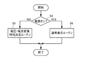
図4は、制御部25が実行する有機LED表示装置制御プログラムのフローチャートであって、CPU251は、まず、外部I/F253を介して有機LED表示装置の電源がオンであるか、オフであるかを判断する(ステップS4)。
FIG. 4 is a flowchart of an organic LED display device control program executed by the
CPU251は、ステップS4で電源がオンからオフに遷移したと判断したときは電圧・電流変換特性決定ルーチンを実行し(ステップS5)、ステップS4で電源がオンであると判断したときは通常表示ルーチンを実行する(ステップS6)。
The
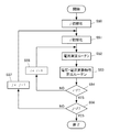
図5は、制御部25が有機LED表示装置制御プログラムのステップS5で実行する電圧・電流変換特性決定ルーチンのフローチャートであって、CPU251は、まず、表示パネル21の行を選択する行選択インデックスjを“1”に初期化する(ステップS50)。
FIG. 5 is a flowchart of a voltage / current conversion characteristic determination routine executed by the
次に、CPU251は、表示パネル21の列を選択する列選択インデックスiを“1”に初期化する(ステップS51)。
Next, the
そして、CPU251は、電流測定ルーチンを実行し(ステップS52)、さらに、電圧・電流変換特性算出ルーチンを実行する(ステップS53)。
Then, the
次に、CPU251は、列選択インデックスiが最大値Iに到達したか否かを判定し(ステップS54)、列選択インデックスiが最大値Iに到達していないと判定したときは、列選択インデックスiをインクリメントして(ステップS55)、ステップS52の処理に戻る。
Next, the
一方、CPU251は、列選択インデックスiが最大値Iに到達したと判定したときは、行選択インデックスjが最大値Jに到達したか否かを判定する(ステップS56)。
On the other hand, when the
CPU251は、行選択インデックスjが最大値Jに到達していないと判定したときは、行選択インデックスjをインクリメントして(ステップS57)、ステップS51の処理に戻る。
When the
一方、CPU251は、行選択インデックスjが最大値Jに到達したと判定したときは、このルーチンを終了する。
On the other hand, when the
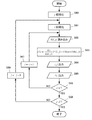
図6は、制御部25が電圧・電流変換特性決定ルーチンのステップS52で実行する電流測定ルーチンのフローチャートであって、CPU251は、まず、電流測定の実行回数を示す回数インデックスmを“1”に初期化する(ステップS520)。
FIG. 6 is a flowchart of the current measurement routine executed by the
次に、CPU251は、列インデックスiを列選択部22に、行インデックスjを行選択部23に、選択信号I/F255を介して出力する(ステップS521)。
Next, the
ついで、CPU251は、D/A変換器254を介して列選択部22の入力端子に第m番目の参照電圧Vr(m)を印加する(ステップS522)。
Next, the
以下に、この状態における画素回路3の動作を、図3を参照しつつ説明する。
Hereinafter, the operation of the
CPU251が行インデックスjを行選択部23に出力すると、行選択線231がオン状態となって第1のFET31のゲートG1に電圧が印加され、第1のFET31が導通状態となる。
When the
CPU251が列インデックスiを列選択部22に出力すると、参照電圧Vr(m)が第1のFET31のソースS1およびドレンD1を経由して第2のFET32のゲートG2に印加される。
When the
すると、参照電圧Vr(m)の関数として決定される電流が、正極線26から第2のFET32のソースS2およびドレンD2を経て有機LED35に流入し、有機LEDを発光させた後、負極線27、電流測定用抵抗素子24を経て、接地線に流出する。
Then, a current determined as a function of the reference voltage Vr (m) flows from the
以下、図6の電流測定ルーチンの説明に戻る。 Hereinafter, the description returns to the current measurement routine of FIG.
CPU251は、電流測定用抵抗素子24の両端に発生した電圧ViをA/D変換器256を介して読み込み、電圧Vi(i、j、m)として記憶する(ステップS523)。
The
CPU251は、回数インデックスmが最大値Mに到達したか否かを判定し(ステップS524)、回数インデックスmが最大値Mに到達していないと判定したときは回数インデックスmをインクリメントして(ステップS525)、ステップS521の処理に戻る。
The
一方、CPU251は、回数インデックスmが最大値Mに到達したと判定したときは、このルーチンを終了する。
On the other hand, when the
図7は、制御部25が電圧・電流変換特性決定ルーチンのステップS53で実行する電圧・電流変換特性算出ルーチンのフローチャートであって、電流測定を2回実施し、電圧・電流変換回路(i、j)の電圧・電流変換特性を、[数1]に示すように電圧を独立変数、電流の開平値を従属変数とする1次関数で近似する場合について説明する。
FIG. 7 is a flowchart of a voltage / current conversion characteristic calculation routine executed by the
CPU251は、電流測定用抵抗素子24の両端に発生した電圧Vi(i、j、1)を電流測定用抵抗素子24の抵抗値Rrで除して、参照電圧Vr(1)を印加したときにi列j行に配置された画素回路3に含まれる有機LED35に流れる電流I1を算出する(ステップS530)。
When the
次に、CPU251は、電流測定用抵抗素子24の両端に発生した電圧Vi(i、j、2)を電流測定用抵抗素子24の抵抗値Rrで除して、参照電圧Vr(2)を印加したときにi列j行に配置された画素回路3に含まれる有機LED35に流れる電流I2を算出する(ステップS531)。
Next, the
CPU251は、[数2]を用いて、i列j行に配置された画素回路3に含まれる第2のFET32の電圧・電流変換特性の比例定数K(i、j)を算出する(ステップS532)。
The
次に、CPU251は、[数3]を用いて、i列j行に配置された画素回路3に含まれる第2のFET32の電圧・電流変換特性の閾値電圧Vth(i、j)を算出して(ステップS533)、このルーチンを終了する。
Next, the
以上で電圧・電流変換特性決定ルーチンの説明を終了し、通常表示時の補正方法について説明する。 This is the end of the description of the voltage / current conversion characteristic determination routine, and a correction method during normal display will be described.
図8は補正方法説明用グラフであって、横軸右方向に電圧・電流変換回路34の第2のFET32のゲートG2に印加される電圧Vを、横軸左方向に第2のFET32のソースS2からドレンD2に向かって流れる電流Iを、縦軸に第2のFET32のソース・ドレン間電圧VSDをとる。
FIG. 8 is a graph for explaining the correction method. The voltage V applied to the gate G2 of the
また、第1象限はゲート電圧V対ソース・ドレン間電圧VSD特性を示し、第2象限は−ソース・ドレン間電圧VSD対ドレン電流I特性を示す。 The first quadrant shows the gate voltage V vs. source-drain voltage V SD characteristics, and the second quadrant shows the source-drain voltage V SD vs. drain current I characteristics.
なお、第1象限のゲート電圧V対ソース・ドレン間電圧VSD特性のうち、実線は標準FETの特性を、一点鎖線はi列j行に配置された画素回路3に含まれる第2のFET32の特性を示す。
Of the gate voltage V versus source-drain voltage V SD characteristics in the first quadrant, the solid line indicates the characteristics of the standard FET, and the alternate long and short dash line indicates the
また、第2象限のソース・ドレン間電圧VSD対ドレン電流I特性は、ソース・ドレン間電圧VSDの1/2乗がドレン電流Iとなる曲線であり、第2のFETによるバラツキはないものとする。 The source-drain voltage V SD vs. drain current I characteristic in the second quadrant is a curve in which the half power of the source-drain voltage V SD becomes the drain current I, and there is no variation due to the second FET. Shall.
従って、i列j行に配置された電圧・電流変換回路34の閾値電圧Vth(i、j)および比例定数K(i、j)が定まれば、第2のFET32のゲート電圧V対ドレン電流I特性が[数4]のように定まる。
Therefore, if the threshold voltage Vth (i, j) and the proportionality constant K (i, j) of the voltage /
標準のFETの輝度電圧V対ソース・ドレン間電圧VSD特性は、[数5]で表されるものとする。 The luminance voltage V vs. source-drain voltage V SD characteristic of a standard FET is expressed by [Equation 5].
よって、標準のFETのゲートに電圧V(i,j)を印加したときに標準のFETのソースからドレンに向かって流れる電流Idが、i列j行に配置された画素回路3に含まれる第2のFET32のゲートに電圧Vcを印加したときに第2のFET32のソースからドレンに向かって流れる電流となるように、電圧Vcを定めればよい。
Therefore, the current Id that flows from the source of the standard FET toward the drain when the voltage V (i, j) is applied to the gate of the standard FET is included in the
図9は、制御部25が有機LED表示装置制御プログラムのステップS6で実行する通常表示ルーチンのフローチャートであって、CPU251は、まず、表示パネル21の行を選択する行選択インデックスjを“1”に初期化する(ステップS60)。
FIG. 9 is a flowchart of a normal display routine executed by the
次に、CPU251は、表示パネル21の列を選択する列選択インデックスiを“1”に初期化する(ステップS61)。
Next, the
CPU251は、i列j行の画素の輝度電圧V(i,j)を外部I/F253を介して読み込む(ステップS62)。
The
そして、CPU251は、[数6]に基づいて補正輝度電圧Vcを算出する(ステップS63)。
Then, the
次に、CPU251は、列インデックスiを列選択部22に、行インデックスjを行選択部23に、選択信号I/F255を介して出力する(ステップS64)。
Next, the
そして、CPU251は、補正輝度電圧Vcを出力する(ステップS65)。
Then, the
次に、CPU251は、列選択インデックスiが最大値Iに到達したか否かを判定し(ステップS66)、列選択インデックスiが最大値Iに到達していないと判定したときは、列選択インデックスiをインクリメントして(ステップS67)、ステップS62の処理に戻る。
Next, the
一方、CPU251は、列選択インデックスiが最大値Iに到達したと判定したときは、行選択インデックスjが最大値Jに到達したか否かを判定する(ステップS68)。
On the other hand, when it is determined that the column selection index i has reached the maximum value I, the
CPU251は、行選択インデックスjが最大値Jに到達していないと判定したときは、行選択インデックスjをインクリメントして(ステップS69)、ステップS61の処理に戻る。
When the
一方、CPU251は、行選択インデックスjが最大値Jに到達したと判定したときは、このルーチンを終了する。
On the other hand, when the
以上説明したように、第1の実施形態によれば、表示パネルに配置される各画素回路の電圧・電流変換特性を測定し、この電圧・電流変換特性に応じて輝度電圧を補正することにより、電圧・電流変換特性のバラツキに起因する輝度のバラツキを補正することができる。
(第2の実施形態)
第1の実施形態にあっては、標準のFETの輝度電圧V対ソース・ドレン間電圧VSD特性は予め定められているものとしているが、理論的に決定されたものであるので実際の特性とは一致しない場合もある。
As described above, according to the first embodiment, the voltage / current conversion characteristic of each pixel circuit arranged in the display panel is measured, and the luminance voltage is corrected according to the voltage / current conversion characteristic. Therefore, it is possible to correct luminance variations caused by variations in voltage / current conversion characteristics.
(Second Embodiment)
In the first embodiment, the luminance voltage V versus the source-drain voltage V SD characteristic of the standard FET is predetermined, but since it is theoretically determined, the actual characteristic May not match.
第2の実施形態は、この課題を解決するものであって、電流測定結果に基づいて標準のFETの輝度電圧V対ソース・ドレン間電圧VSD特性を決定する。 The second embodiment solves this problem, and determines the luminance voltage V vs. source-drain voltage V SD characteristics of a standard FET based on the current measurement result.
図10は、第2の実施形態で使用される第2の電圧・電流変換特性決定ルーチンのフローチャートであって、ステップS53とステップS54の間に基準特性決定ルーチン(ステップS7)が挿入される。 FIG. 10 is a flowchart of a second voltage / current conversion characteristic determination routine used in the second embodiment, and a reference characteristic determination routine (step S7) is inserted between step S53 and step S54.
図11は、基準電圧・電流変換特性決定ルーチンのフローチャートであって、表示パネルを構成する複数の画素回路の輝度電圧V対ソース・ドレン間電圧VSD特性の平均特性を標準の輝度電圧V対ソース・ドレン間電圧VSD特性とする場合を示している。 FIG. 11 is a flowchart of a reference voltage / current conversion characteristic determination routine, in which the average characteristic of the luminance voltage V vs. source-drain voltage V SD characteristics of a plurality of pixel circuits constituting the display panel is expressed as a standard luminance voltage V vs. The source-drain voltage V SD characteristics are shown.
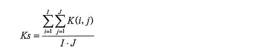
まず、CPU251は、[数7]により図7に示す電圧・電流変換特性算出ルーチンのステップS532で算出された比例定数の平均値を標準の輝度電圧V対ソース・ドレン間電圧VSD特性の比例定数とする(ステップS70)。
First, the
次に、CPU251は、[数8]により図7に示す電圧・電流変換特性算出ルーチンのステップS533で算出された閾値電圧の平均値を標準の輝度電圧V対ソース・ドレン間電圧VSD特性の閾値電圧とする(ステップS71)。
Next, the
以上説明したように、第2の実施形態によれば、実際の表示パネルに基づいて標準の輝度電圧V対ソース・ドレン間電圧VSD特性を決定することが可能となる。 As described above, according to the second embodiment, it is possible to determine the standard luminance voltage V vs. source-drain voltage V SD characteristic based on the actual display panel.
11 表示手段
12 電圧・電流変換特性決定手段
13 輝度電圧補正手段
121 参照電圧印加手段
122 電流計測手段
123 電圧・電流変換特性算出手段
DESCRIPTION OF
Claims (5)
前記電圧・電流変換回路のそれぞれの電圧・電流変換特性を決定する電圧・電流変換特性決定手段と、
前記電圧・電流変換回路に供給される前記輝度電圧を前記電圧・電流変換特性決定手段で決定された電圧・電流変換特性に基づいて補正する輝度電圧補正手段とを含む有機LED表示装置。 A display configured by arranging a plurality of pixel circuits in a matrix form, each of which includes an organic LED and a voltage / current conversion circuit that converts a luminance voltage for controlling the luminance when the organic LED emits light into a luminance current supplied to the organic LED Means,
Voltage / current conversion characteristic determining means for determining each voltage / current conversion characteristic of the voltage / current conversion circuit;
An organic LED display device comprising: a luminance voltage correction unit that corrects the luminance voltage supplied to the voltage / current conversion circuit based on the voltage / current conversion characteristic determined by the voltage / current conversion characteristic determination unit.
前記電圧・電流変換回路のそれぞれに、参照電圧を印加する参照電圧印加手段と、
前記参照電圧印加手段から参照電圧が印加されたときに、前記電圧・電流変換回路を介して前記有機LEDに流れる電流を計測する電流計測手段と、
前記参照電圧印加手段により印加された参照電圧と前記電流測定手段で測定された電流とに基づいて前記電圧・電流変換回路のそれぞれの電圧・電流変換特性を算出する電圧・電流変換特性算出手段とを含む請求項1に記載の有機LED表示装置。 The voltage / current conversion characteristic determining means includes:
Reference voltage application means for applying a reference voltage to each of the voltage / current conversion circuits;
Current measuring means for measuring a current flowing through the organic LED via the voltage / current conversion circuit when a reference voltage is applied from the reference voltage applying means;
Voltage / current conversion characteristic calculating means for calculating each voltage / current conversion characteristic of the voltage / current conversion circuit based on the reference voltage applied by the reference voltage applying means and the current measured by the current measuring means; The organic LED display device according to claim 1, comprising:
前記電流計測手段が、前記少なくとも2つの参照電圧が印加されたときに、前記電圧・電流変換回路を介して前記有機LEDに流れる少なくとも2つの電流を計測するものであり、
前記電圧・電流変換特性算出手段が、前記参照電圧印加手段により印加された少なくとも2つの参照電圧と前記電流測定手段で測定された少なくとも2つの電流とに基づいて、前記電圧・電流変換特性を、電圧を独立変数、電流の開平値を従属変数とする1次関数で表したときの比例定数および電圧軸切片である閾値電圧を算出するものである請求項2に記載の有機LED表示装置。 The reference voltage applying means applies at least two different reference voltages to each of the voltage / current conversion circuits;
The current measuring means measures at least two currents flowing through the organic LED via the voltage / current conversion circuit when the at least two reference voltages are applied;
Based on at least two reference voltages applied by the reference voltage applying unit and at least two currents measured by the current measuring unit, the voltage / current conversion characteristic calculating unit calculates the voltage / current conversion characteristic, The organic LED display device according to claim 2, which calculates a proportionality constant and a threshold voltage which is a voltage axis intercept when the voltage is represented by a linear function having an independent variable and a square root value of a current as a dependent variable.
前記輝度電圧を、前記電圧・電流変換特性算出手段で算出された電圧・電流変換特性と基準電圧・電流変換特性とに基づいて補正するものである請求項3に記載の有機LED表示装置。 The luminance voltage correcting means is
4. The organic LED display device according to claim 3, wherein the luminance voltage is corrected based on the voltage / current conversion characteristic calculated by the voltage / current conversion characteristic calculation means and a reference voltage / current conversion characteristic.
前記電圧・電流変換特性算出手段で算出された電圧・電流変換特性に基づいて決定される請求項4に記載の有機LED表示装置。 The reference voltage / current conversion characteristic is
The organic LED display device according to claim 4, wherein the organic LED display device is determined based on the voltage / current conversion characteristics calculated by the voltage / current conversion characteristics calculation means.
Priority Applications (1)
| Application Number | Priority Date | Filing Date | Title |
|---|---|---|---|
| JP2005194974A JP2007011205A (en) | 2005-07-04 | 2005-07-04 | Organic led display device |
Applications Claiming Priority (1)
| Application Number | Priority Date | Filing Date | Title |
|---|---|---|---|
| JP2005194974A JP2007011205A (en) | 2005-07-04 | 2005-07-04 | Organic led display device |
Publications (1)
| Publication Number | Publication Date |
|---|---|
| JP2007011205A true JP2007011205A (en) | 2007-01-18 |
Family
ID=37749770
Family Applications (1)
| Application Number | Title | Priority Date | Filing Date |
|---|---|---|---|
| JP2005194974A Pending JP2007011205A (en) | 2005-07-04 | 2005-07-04 | Organic led display device |
Country Status (1)
| Country | Link |
|---|---|
| JP (1) | JP2007011205A (en) |
Citations (5)
| Publication number | Priority date | Publication date | Assignee | Title |
|---|---|---|---|---|
| JPH11219146A (en) * | 1997-09-29 | 1999-08-10 | Mitsubishi Chemical Corp | Active matrix light emitting diode picture element structure and method |
| JP2002278514A (en) * | 2001-03-19 | 2002-09-27 | Sharp Corp | Electro-optical device |
| JP2004094237A (en) * | 2002-08-14 | 2004-03-25 | Rohm Co Ltd | Organic el drive circuit and organic el display device using the same |
| JP2004145257A (en) * | 2002-04-23 | 2004-05-20 | Semiconductor Energy Lab Co Ltd | Light emitting device device and production system of the same |
| WO2005057544A1 (en) * | 2003-12-10 | 2005-06-23 | Koninklijke Philips Electronics N.V. | Video data signal correction |
-
2005
- 2005-07-04 JP JP2005194974A patent/JP2007011205A/en active Pending
Patent Citations (5)
| Publication number | Priority date | Publication date | Assignee | Title |
|---|---|---|---|---|
| JPH11219146A (en) * | 1997-09-29 | 1999-08-10 | Mitsubishi Chemical Corp | Active matrix light emitting diode picture element structure and method |
| JP2002278514A (en) * | 2001-03-19 | 2002-09-27 | Sharp Corp | Electro-optical device |
| JP2004145257A (en) * | 2002-04-23 | 2004-05-20 | Semiconductor Energy Lab Co Ltd | Light emitting device device and production system of the same |
| JP2004094237A (en) * | 2002-08-14 | 2004-03-25 | Rohm Co Ltd | Organic el drive circuit and organic el display device using the same |
| WO2005057544A1 (en) * | 2003-12-10 | 2005-06-23 | Koninklijke Philips Electronics N.V. | Video data signal correction |
Similar Documents
| Publication | Publication Date | Title |
|---|---|---|
| EP3472826B1 (en) | Calibration apparatus for oled sub-pixel circuit, source electrode driving circuit, and data voltage compensation method | |
| US7345660B2 (en) | Correction of pixels in an organic EL display device | |
| JP5443504B2 (en) | Method for providing drive transistor control signal to drive transistor | |
| US7656370B2 (en) | Method and circuit arrangement for the ageing compensation of an organic light-emitting diode and circuit arrangement | |
| TWI449017B (en) | Electroluminescent display with initial nonuniformity compensation | |
| JP5416229B2 (en) | Electroluminescent display compensated drive signal | |
| CN107452342B (en) | Display system, control system, analysis method of display panel and test system | |
| US8427513B2 (en) | Display device, display device drive method, and computer program | |
| US9202412B2 (en) | Organic EL display apparatus and method of fabricating organic EL display apparatus | |
| US9576530B2 (en) | Electro-optical device | |
| TWI383356B (en) | Electroluminescent display compensated analog transistor drive signal | |
| US8059070B2 (en) | Display device, and methods for manufacturing and controlling the display device | |
| US8072400B2 (en) | Measurement of pixel current in display device | |
| US10276095B2 (en) | Display device and method of driving display device | |
| US20090256854A1 (en) | Brightness unevenness correction for oled | |
| JP2010517092A5 (en) | ||
| JP2012513040A (en) | Digitally driven electroluminescent display compensated for aging | |
| JP5807007B2 (en) | Display device | |
| JP2004138831A (en) | Organic electroluminescence display device | |
| CA2490860A1 (en) | Real-time calibration scheduling method and algorithm for amoled displays | |
| KR20140095425A (en) | Driving method of display apparatus | |
| JP2005070614A (en) | Method for inspecting organic el substrate and organic el display device | |
| KR20160007787A (en) | Organic light emitting display and method for driving the same | |
| JP6312083B2 (en) | Display device and driving method thereof | |
| US20080088567A1 (en) | Method and device for measuring panel current |
Legal Events
| Date | Code | Title | Description |
|---|---|---|---|
| A621 | Written request for application examination |
Free format text: JAPANESE INTERMEDIATE CODE: A621 Effective date: 20080122 |
|
| A131 | Notification of reasons for refusal |
Free format text: JAPANESE INTERMEDIATE CODE: A131 Effective date: 20101228 |
|
| A02 | Decision of refusal |
Free format text: JAPANESE INTERMEDIATE CODE: A02 Effective date: 20110426 |