JP2007010403A - Measuring technique for film thickness of antireflective layer of antireflective film - Google Patents
Measuring technique for film thickness of antireflective layer of antireflective film Download PDFInfo
- Publication number
- JP2007010403A JP2007010403A JP2005189585A JP2005189585A JP2007010403A JP 2007010403 A JP2007010403 A JP 2007010403A JP 2005189585 A JP2005189585 A JP 2005189585A JP 2005189585 A JP2005189585 A JP 2005189585A JP 2007010403 A JP2007010403 A JP 2007010403A
- Authority
- JP
- Japan
- Prior art keywords
- film
- light
- antireflective
- film thickness
- thickness
- Prior art date
- Legal status (The legal status is an assumption and is not a legal conclusion. Google has not performed a legal analysis and makes no representation as to the accuracy of the status listed.)
- Granted
Links
Images
Abstract
Description
本発明は、反射防止フィルムの透明反射防止層の膜厚を測定する方法に関するものである。 The present invention relates to a method for measuring the film thickness of a transparent antireflection layer of an antireflection film.
反射防止フィルムの反射防止層の膜厚を測定する方法として一般的なのが、可視光を用いてその分光特性により、正常な厚さの分光特性と比較して厚さを算出するものである。しかし、この方法によると、ポイントでとらえることはできるが、大きなフィルム全面の膜厚分布等はとることができない。時間をかければ測定ポイントを増やし、マップを作成することも出来るが、ラインで流れているような状態で全巾を測定することは出来ない。 As a general method for measuring the film thickness of the antireflection layer of the antireflection film, the thickness is calculated by comparing the spectral characteristics of normal thickness with the spectral characteristics using visible light. However, according to this method, although it can be grasped by points, the film thickness distribution on the entire surface of the large film cannot be obtained. If you take time, you can increase the number of measurement points and create a map, but you cannot measure the full width as if it is flowing in a line.
ディスプレイの表面に貼られている反射防止フィルムの反射防止作用は、主につや消しのフィルムを用いる方法と、薄膜の干渉を用いた二種類のものがある。 The antireflection action of the antireflection film attached to the surface of the display is mainly classified into a method using a matte film and two types using thin film interference.
薄膜の干渉を用いた反射防止フィルムの反射防止層は、主に可視光の中心値540nm付近の緑色の波長を干渉で打ち消すよう、540nm×1/4の厚さに設定された反射防止膜が存在する。540nm×1/4=135nmで屈折率を1.36程度の物質で構成させると、およそ100nm程の厚さで塗られている。この層の厚さの変動があると、正しく540nmで干渉を起こさなくなり、干渉を起こす波長域が変動し、目視ではムラに見えることがある。また、急激な厚さ変動、凹部、凸部が存在すると、点欠陥としてとらえてしまう。 The anti-reflection layer of the anti-reflection film using the interference of the thin film is an anti-reflection film set to a thickness of 540 nm × ¼ so that the green wavelength near the center value of 540 nm of visible light is mainly canceled by interference. Exists. When it is made of a material having a refractive index of about 1.36 at 540 nm × 1/4 = 135 nm, it is coated with a thickness of about 100 nm. If there is a variation in the thickness of this layer, interference does not occur correctly at 540 nm, the wavelength range causing the interference varies, and visual observation may appear uneven. Further, if there is a sudden thickness variation, a concave portion, or a convex portion, it is regarded as a point defect.
そのため、この反射防止膜の層の厚さはかなり均一なものである必要があり、反射防止フィルムの製造中、ラインで流れているような状態でフィルム全巾で反射防止層の膜厚を常時管理する必要がある。 For this reason, the thickness of the antireflection film must be fairly uniform. During the production of the antireflection film, the thickness of the antireflection layer should always be set to the full width of the film as if it were flowing in a line. Need to manage.
本発明は、上記の課題を解決するためになされたものであって、反射防止フィルムの製造中、フィルム走行状態でフィルム全巾にわたり連続的に反射防止層の膜厚を測定することが可能な、反射防止フィルムの反射防止層の膜厚を測定する方法を提供することを目的とする。 The present invention has been made to solve the above-described problem, and during the production of an antireflection film, the film thickness of the antireflection layer can be continuously measured over the entire width of the film while the film is running. An object of the present invention is to provide a method for measuring the film thickness of an antireflection layer of an antireflection film.
上記の目的を達成するために、すなわち、請求項1に係る発明は、反射防止フィルムの反射防止層の膜面に365〜400nmの長波長域紫外光を照射し、その膜面および膜の裏面からの反射光を相互に干渉させ、その干渉により得らた濃淡の光像(光信号)によって薄膜の膜厚を測定することを特徴とする反射防止フィルムの反射防止層の膜厚を測定する方法である。 In order to achieve the above object, that is, in the invention according to claim 1, the film surface of the antireflection layer of the antireflection film is irradiated with ultraviolet light having a long wavelength region of 365 to 400 nm, and the film surface and the back surface of the film The thickness of the antireflection layer of the antireflection film is measured by measuring the thickness of the thin film based on the light image (light signal) of light and shade obtained by the interference between the reflected lights from Is the method.
本発明により、ウエブ状の反射防止フィルムの製造中、フィルム走行状態でフィルム全巾にわたり連続的に反射防止層の膜厚を測定することが可能となった。この測定方法により、反射防止フィルムの製造中、反射防止層の均一な膜厚の管理が可能となった。 The present invention makes it possible to continuously measure the film thickness of the antireflection layer over the entire width of the film during the production of the web-like antireflection film. This measurement method enabled management of the uniform thickness of the antireflection layer during the production of the antireflection film.
通常、反射防止層は100nm、屈折率1.35程度の透明樹脂で構成される。この構
成であれば、前述したとおり、およそ可視光400〜750nmの中心値540nmの緑付近の波長の1/4の長さであるため、この層に入射する可視光は540nmを中心として干渉を起こし、反射してこなくなる。
Usually, the antireflection layer is made of a transparent resin having a thickness of 100 nm and a refractive index of about 1.35. With this configuration, as described above, the visible light incident on this layer interferes with the center at 540 nm because the length is about ¼ of the wavelength in the vicinity of green with a central value of 540 nm of visible light 400 to 750 nm. Wake up and not reflect.
540nmから遠ざかれば、例えば、400nmや750nmの光は干渉を起こしきれない分、わずかに反射してくる。従って、この層の厚さが変化することで、反射してくる光の分光特性が変わり、その反射してくるわずかな光の構成も変わってくる。これが従来の膜厚測定方法である。 When moving away from 540 nm, for example, light of 400 nm or 750 nm is slightly reflected as much as interference cannot occur. Therefore, by changing the thickness of this layer, the spectral characteristics of the reflected light change, and the composition of the slight reflected light also changes. This is a conventional film thickness measurement method.
上記の従来の膜厚測定方法に対して、本発明の膜厚測定方法によれば、380nm程度の可視光域に近い紫外線の場合である。380nm×1/4=95nm、95nm×1.35=66.7nm、すなわち、膜厚66.7nmのとき全干渉を起こし、130nm程度でも全干渉を起こす。厚さ66.7nmのときは、UV波長380nmの1/4波長なので、反射光は最も少ない状態となる。 In contrast to the above-described conventional film thickness measurement method, according to the film thickness measurement method of the present invention, this is the case of ultraviolet rays close to the visible light range of about 380 nm. 380 nm × 1/4 = 95 nm, 95 nm × 1.35 = 66.7 nm, that is, total interference occurs when the film thickness is 66.7 nm, and total interference occurs even at about 130 nm. When the thickness is 66.7 nm, the reflected light is the least because it is a quarter wavelength of the UV wavelength of 380 nm.
また、130nmの場合は、1/2波長なので反射光は倍増され、最も明るくなる。従って、66.7〜130nmの間で膜厚が変化するのであれば、380nm程度の紫外光を用いることで、100nmを中心に厚さの変化がそのままの明暗で表示されることになる。 In the case of 130 nm, since the wavelength is ½, the reflected light is doubled and becomes brightest. Therefore, if the film thickness changes between 66.7 and 130 nm, the change in the thickness centered on 100 nm is displayed as it is by using the ultraviolet light of about 380 nm.
以下、本発明の反射防止フィルムの反射防止層の膜厚を測定する方法において、直線ライン状紫外照明光を用いた測定装置を用いた一実施形態について図面を参照して詳細に説明する。 Hereinafter, in the method for measuring the film thickness of the antireflection layer of the antireflection film of the present invention, an embodiment using a measuring device using linear linear ultraviolet illumination light will be described in detail with reference to the drawings.
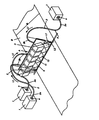
図1は、本発明装置Aの全体斜視図であり、1は、紫外波長域を含む光源装置、4は、可視光源装置より発する光の波長域のうち前記干渉を起こす紫外波長域の光を選択する紫外光透過光学フィルター、2は、光源装置1の光発生位置に基端部2aが接続されて、該光源装置1から発する紫外波長域を含む可視光をライン状にガイドするライン状ライトガイド、3は、そのライン状ライトガイド2の先端部2bが接続された矩形状のプレート状ライトガイド、11は、CCDカメラ等の光像検出手段、12は、紫外域波長360nm以上400nm未満の紫外域の長波長側に60〜70%程度の高い透過率を持つ撮像レンズ部(例えば光学ガラスBK7を用いた高透過率レンズ)、Bは、被検査体、Sは被検査体Bの幅W方向に照射された照明幅dの直線ライン状紫外照明光である。
FIG. 1 is an overall perspective view of the device A of the present invention, in which 1 is a light source device including an ultraviolet wavelength region, and 4 is light in an ultraviolet wavelength region that causes interference among the wavelength regions of light emitted from a visible light source device. The ultraviolet light transmitting
前記矩形状のプレート状ライトガイド3は、その下端部を被検査体Bに向かって、その検査体Bの幅W方向に平行に固定配置されている。 The rectangular plate-shaped light guide 3 is fixedly arranged parallel to the width W direction of the inspection object B with its lower end directed toward the inspection object B.
前記光源装置1から発した紫外波長域を含む可視光は、紫外波長域の光を選択する紫外光透過光学フィルター4を透って、ライン状ライトガイドの干渉を起こす紫外波長域のみの光L1を、該光源装置1に接続したライン状ライトガイド2の基端部2aに入射し、その基端部2aからライン状ライトガイド2に沿って、そのガイド2先端部2bにライン状にガイドする。
Visible light including the ultraviolet wavelength region emitted from the light source device 1 passes through the ultraviolet light transmission optical filter 4 that selects light in the ultraviolet wavelength region, and only the light L1 in the ultraviolet wavelength region causing interference of the linear light guide. Is incident on the base end portion 2a of the line-
ライン状ライトガイド2の先端部2bは、被検査体Bの幅W方向に平行に固定配置した矩形状のプレート状ライトガイド3の上端部に接続して取り付けられていて、紫外波長域のみの光L1はライン状ライトガイド2の先端部2bからプレート状ライトガイド3内部に照射され、そのガイド3内部を透って下端部から、照明幅dの直線ライン状紫外照明光L1として、被検査体Bの表面に照射されるようになっている。なお、本発明装置において、光源装置1は1基乃至複数基を配置することができ、また、ライン状ライトガイド2は、各光源装置1に対して1本乃至複数本を接続することができ、また、プレート状ライ
トガイド3の上端部に対しては1本乃至複数本を接続することができる。
The front end portion 2b of the line-
図1に示す紫外波長域を含む光源装置1は、水銀放電ランプを用いた紫外波長域を多く含む可視光も発するランプハウス型の光源装置であり、このランプから発する光線は紫外光域から可視光域までの様々な波長の光を発するものであり、実際は、200nm〜700nm近傍までの様々な波長の光が発せられる。 The light source device 1 including the ultraviolet wavelength region shown in FIG. 1 is a lamp house type light source device that emits visible light including a large amount of ultraviolet wavelength region using a mercury discharge lamp, and the light emitted from this lamp is visible from the ultraviolet light region. It emits light of various wavelengths up to the light range, and actually, light of various wavelengths from 200 nm to 700 nm is emitted.
200nm〜700nm近傍までの様々な波長のうち、可視光域の波長は、400nm以上〜700nm以下程度であるが、紫外光域の波長は、200nm〜400nm未満程度であり、その紫外光域の波長の中では、特に300nm〜400未満nm、あるいは360nm〜400nm未満程度までの紫外光が最も強く発せられる。 Among various wavelengths from 200 nm to near 700 nm, the wavelength in the visible light region is about 400 nm to 700 nm, but the wavelength in the ultraviolet region is about 200 nm to less than 400 nm, and the wavelength in the ultraviolet region. In particular, ultraviolet light having a wavelength of about 300 nm to less than 400 nm or about 360 nm to less than 400 nm is emitted most strongly.
本発明装置のように紫外波長域を含む光源装置1による光源を使う直線ライン状紫外照明光Lによる照明検査の場合、まず、光像検出手段11であるカメラ(例えば、リニア型CCDカメラ)の感度は、紫外光専用カメラを使わない限りは、紫外光域よりも可視光域に強く出ているため、たとえ紫外光によって被検査体の何かを光像として検出したとしても、よりカメラ感度の高い可視光によって紫外光による被検査体の光像は全て消されてしまうか、映像として判別し難くなる。 In the case of the illumination inspection by the linear line-shaped ultraviolet illumination light L using the light source by the light source device 1 including the ultraviolet wavelength region as in the device of the present invention, first, a camera (for example, a linear CCD camera) as the optical image detection means 11 is used. Sensitivity is higher in the visible light range than in the ultraviolet light range unless a dedicated camera for ultraviolet light is used, so even if something on the object to be inspected is detected as an optical image by ultraviolet light, the camera sensitivity is higher. The high visible light erases all the light image of the object to be inspected by ultraviolet light or makes it difficult to discriminate it as an image.
そのために、紫外波長域を含む可視光源装置1による光源光のうち、波長400nm以上の可視光は全てカットして、紫外光のみとする必要がある。また、紫外光であっても、350nm以下の短波長の紫外光は、ライン状ライトガイド2、プレート状ライトガイド3などのライトガイドに一般的に用いられる多成分グラスファイバーや、レンズに劣化をもたらす現象があるため、石英製のファイバーやレンズを使わない限り、これもまたカットする必要がある。石英製の場合はその限りでない。
Therefore, it is necessary to cut all visible light having a wavelength of 400 nm or more from the light source light by the visible light source device 1 including the ultraviolet wavelength region so that only the ultraviolet light is obtained. Even in the case of ultraviolet light, ultraviolet light having a short wavelength of 350 nm or less deteriorates multi-component glass fibers or lenses generally used for light guides such as the
よって、本発明装置においては、紫外波長域を含む可視光源装置1のランプハウス中には、波長350nm〜400nm未満までの光L1を透すフィルター4が装着されるものである。 Therefore, in the device of the present invention, the filter 4 that transmits the light L1 having a wavelength of 350 nm to less than 400 nm is mounted in the lamp house of the visible light source device 1 including the ultraviolet wavelength region.
可視光源装置1からは、ライン状ライトガイド2とプレート状ライトガイド3とがこの順に接続され、フィルター4を透過した光L1を、プレート状ライトガイド3によって照明幅dの直線ライン状紫外照明光L1として、その照明光L1によって照明された被検査体B(例えば、連続的に移動するシートB、あるいは静止状態のシートB)の表面にて反射した反射光L2による光像が、光像検出手段11のレンズ12を通して、リニア型CCDカメラ(ラインCCDカメラ)等の光像検出手段11にて撮像される。
From the visible light source device 1, a line-
撮像されるこの画像により、正常厚みの部分はおよそ128階調に、それ以上厚い部分は白っぽく薄いところは暗く表示される。 According to this captured image, the normal thickness portion is displayed in about 128 gradations, and the thicker portion is displayed in a whitish and thin portion dark.
上記の反射防止フィルムの反射防止層の膜厚を測定する方法により、ウエブ状の反射防止フィルムの製造中、フィルム走行状態でフィルム全巾にわたり連続的に反射防止層の膜厚を測定することができる。この測定方法により、反射防止フィルムの製造中、反射防止層の均一な膜厚の管理が可能となる。 According to the method for measuring the film thickness of the antireflection layer of the antireflection film, the film thickness of the antireflection layer can be continuously measured over the entire width of the film during the production of the web-shaped antireflection film. it can. This measurement method enables management of the uniform thickness of the antireflection layer during the production of the antireflection film.
A…検査装置
B…被検査体
1…紫外光を含む可視光源装置
2…ライン状ライトガイド
2a…ガイド基端部
2b…先端部
3…プレート状ライトガイド
4…光学フィルター
11…光像検出手段
12…光学レンズ部
A ... inspection device B ... inspected object 1 ... visible
Claims (1)
Priority Applications (1)
| Application Number | Priority Date | Filing Date | Title |
|---|---|---|---|
| JP2005189585A JP5181412B2 (en) | 2005-06-29 | 2005-06-29 | Method for controlling the film thickness of the antireflection layer of the antireflection film |
Applications Claiming Priority (1)
| Application Number | Priority Date | Filing Date | Title |
|---|---|---|---|
| JP2005189585A JP5181412B2 (en) | 2005-06-29 | 2005-06-29 | Method for controlling the film thickness of the antireflection layer of the antireflection film |
Publications (2)
| Publication Number | Publication Date |
|---|---|
| JP2007010403A true JP2007010403A (en) | 2007-01-18 |
| JP5181412B2 JP5181412B2 (en) | 2013-04-10 |
Family
ID=37749128
Family Applications (1)
| Application Number | Title | Priority Date | Filing Date |
|---|---|---|---|
| JP2005189585A Expired - Fee Related JP5181412B2 (en) | 2005-06-29 | 2005-06-29 | Method for controlling the film thickness of the antireflection layer of the antireflection film |
Country Status (1)
| Country | Link |
|---|---|
| JP (1) | JP5181412B2 (en) |
Cited By (1)
| Publication number | Priority date | Publication date | Assignee | Title |
|---|---|---|---|---|
| JP2012068173A (en) * | 2010-09-24 | 2012-04-05 | Fujifilm Corp | Method for measuring film thickness of optical film and method for manufacturing optical film |
Citations (9)
| Publication number | Priority date | Publication date | Assignee | Title |
|---|---|---|---|---|
| JPS5974354U (en) * | 1982-11-11 | 1984-05-19 | 大日本印刷株式会社 | Line optical head |
| JPS6399263U (en) * | 1986-12-19 | 1988-06-27 | ||
| JP2000241127A (en) * | 1999-02-25 | 2000-09-08 | Toppan Printing Co Ltd | Film thickness measurement method and winding-up vacuum film-forming device |
| JP2002310924A (en) * | 2001-04-17 | 2002-10-23 | Toray Ind Inc | Sheet defect inspecting device and sheet manufacturing method |
| JP2003042971A (en) * | 2001-07-31 | 2003-02-13 | Ibiden Co Ltd | Pattern inspection device and inspection method |
| JP2004012254A (en) * | 2002-06-06 | 2004-01-15 | Toshiba Corp | Surface inspection device |
| JP2004107690A (en) * | 2002-09-13 | 2004-04-08 | Konica Minolta Holdings Inc | Method for depositing optical thin film, method for producing antireflection film and antireflection film |
| JP2006038728A (en) * | 2004-07-29 | 2006-02-09 | Toppan Printing Co Ltd | Method for inspecting antireflection transparent film |
| JP2006258880A (en) * | 2005-03-15 | 2006-09-28 | Konica Minolta Opto Inc | Method for manufacturing antireflection film, and antireflection film |
-
2005
- 2005-06-29 JP JP2005189585A patent/JP5181412B2/en not_active Expired - Fee Related
Patent Citations (9)
| Publication number | Priority date | Publication date | Assignee | Title |
|---|---|---|---|---|
| JPS5974354U (en) * | 1982-11-11 | 1984-05-19 | 大日本印刷株式会社 | Line optical head |
| JPS6399263U (en) * | 1986-12-19 | 1988-06-27 | ||
| JP2000241127A (en) * | 1999-02-25 | 2000-09-08 | Toppan Printing Co Ltd | Film thickness measurement method and winding-up vacuum film-forming device |
| JP2002310924A (en) * | 2001-04-17 | 2002-10-23 | Toray Ind Inc | Sheet defect inspecting device and sheet manufacturing method |
| JP2003042971A (en) * | 2001-07-31 | 2003-02-13 | Ibiden Co Ltd | Pattern inspection device and inspection method |
| JP2004012254A (en) * | 2002-06-06 | 2004-01-15 | Toshiba Corp | Surface inspection device |
| JP2004107690A (en) * | 2002-09-13 | 2004-04-08 | Konica Minolta Holdings Inc | Method for depositing optical thin film, method for producing antireflection film and antireflection film |
| JP2006038728A (en) * | 2004-07-29 | 2006-02-09 | Toppan Printing Co Ltd | Method for inspecting antireflection transparent film |
| JP2006258880A (en) * | 2005-03-15 | 2006-09-28 | Konica Minolta Opto Inc | Method for manufacturing antireflection film, and antireflection film |
Cited By (1)
| Publication number | Priority date | Publication date | Assignee | Title |
|---|---|---|---|---|
| JP2012068173A (en) * | 2010-09-24 | 2012-04-05 | Fujifilm Corp | Method for measuring film thickness of optical film and method for manufacturing optical film |
Also Published As
| Publication number | Publication date |
|---|---|
| JP5181412B2 (en) | 2013-04-10 |
Similar Documents
| Publication | Publication Date | Title |
|---|---|---|
| WO2016188378A1 (en) | Measurement device and measurement method for thin film provided with transparent substrate | |
| US10311271B2 (en) | Diffuse bright field illumination system for a barcode reader | |
| US9788732B2 (en) | Optical measuring device and fiber bundle association method | |
| JP2015200664A (en) | Device for angular colorimetry and method of the same | |
| TWI451073B (en) | Measuring the optical system and the use of its brightness meter, color brightness meter and color meter | |
| CN103105403A (en) | Method and device for detecting surface defect of transparent optical component | |
| JP2006266933A (en) | Method and apparatus for inspecting defect in transparent plate | |
| JP2002181698A (en) | Spectral reflectance measuring apparatus and method | |
| CN203069531U (en) | Device for detecting surface defect of transparent optical element | |
| JP2008170344A (en) | Evaluating method and measuring device of glareproof | |
| US9250184B2 (en) | Status estimation device, status estimation method and program for ultraviolet curable resin | |
| JP2007333563A (en) | Inspection device and inspection method for light transmitting sheet | |
| KR101738188B1 (en) | Relief pattern detection device | |
| CN205449356U (en) | Glass surface stress appearance | |
| JP5181412B2 (en) | Method for controlling the film thickness of the antireflection layer of the antireflection film | |
| CN103579037A (en) | Thickness detection apparatus using digital optical technology and method using the same | |
| JP2006201015A (en) | Inspection device using linear line like ultraviolet illumination light | |
| FI127243B (en) | Method and measuring device for continuous measurement of Abbe number | |
| JP2016114602A (en) | Surface shape measurement device, and defect determination device | |
| CN106500891B (en) | Glass surface stress detection device and detection prism used for same | |
| JP5184842B2 (en) | Colored film thickness measuring method and apparatus | |
| JPH03276005A (en) | Shape measuring device | |
| CN216594853U (en) | Defect detection device for transparent medium thin layer | |
| KR20130080269A (en) | Displacement measuring apparatus, and displacement measuring method using the same | |
| JPH095167A (en) | Ear drum thermometer |
Legal Events
| Date | Code | Title | Description |
|---|---|---|---|
| A621 | Written request for application examination |
Free format text: JAPANESE INTERMEDIATE CODE: A621 Effective date: 20080522 |
|
| A977 | Report on retrieval |
Free format text: JAPANESE INTERMEDIATE CODE: A971007 Effective date: 20101019 |
|
| A131 | Notification of reasons for refusal |
Free format text: JAPANESE INTERMEDIATE CODE: A131 Effective date: 20101026 |
|
| A521 | Written amendment |
Free format text: JAPANESE INTERMEDIATE CODE: A523 Effective date: 20101217 |
|
| A131 | Notification of reasons for refusal |
Free format text: JAPANESE INTERMEDIATE CODE: A131 Effective date: 20110920 |
|
| A131 | Notification of reasons for refusal |
Free format text: JAPANESE INTERMEDIATE CODE: A131 Effective date: 20121002 |
|
| A521 | Written amendment |
Free format text: JAPANESE INTERMEDIATE CODE: A523 Effective date: 20121127 |
|
| TRDD | Decision of grant or rejection written | ||
| A01 | Written decision to grant a patent or to grant a registration (utility model) |
Free format text: JAPANESE INTERMEDIATE CODE: A01 Effective date: 20121218 |
|
| A61 | First payment of annual fees (during grant procedure) |
Free format text: JAPANESE INTERMEDIATE CODE: A61 Effective date: 20121231 |
|
| R150 | Certificate of patent or registration of utility model |
Free format text: JAPANESE INTERMEDIATE CODE: R150 |
|
| FPAY | Renewal fee payment (event date is renewal date of database) |
Free format text: PAYMENT UNTIL: 20160125 Year of fee payment: 3 |
|
| LAPS | Cancellation because of no payment of annual fees |