JP2006524914A - Plasma processing system and method - Google Patents
Plasma processing system and method Download PDFInfo
- Publication number
- JP2006524914A JP2006524914A JP2006508616A JP2006508616A JP2006524914A JP 2006524914 A JP2006524914 A JP 2006524914A JP 2006508616 A JP2006508616 A JP 2006508616A JP 2006508616 A JP2006508616 A JP 2006508616A JP 2006524914 A JP2006524914 A JP 2006524914A
- Authority
- JP
- Japan
- Prior art keywords
- chamber
- plasma processing
- particles
- processing system
- electrode
- Prior art date
- Legal status (The legal status is an assumption and is not a legal conclusion. Google has not performed a legal analysis and makes no representation as to the accuracy of the status listed.)
- Withdrawn
Links
Images


Classifications
-
- H—ELECTRICITY
- H01—ELECTRIC ELEMENTS
- H01J—ELECTRIC DISCHARGE TUBES OR DISCHARGE LAMPS
- H01J37/00—Discharge tubes with provision for introducing objects or material to be exposed to the discharge, e.g. for the purpose of examination or processing thereof
- H01J37/32—Gas-filled discharge tubes
- H01J37/32431—Constructional details of the reactor
- H01J37/3244—Gas supply means
-
- H—ELECTRICITY
- H01—ELECTRIC ELEMENTS
- H01J—ELECTRIC DISCHARGE TUBES OR DISCHARGE LAMPS
- H01J2237/00—Discharge tubes exposing object to beam, e.g. for analysis treatment, etching, imaging
- H01J2237/02—Details
- H01J2237/022—Avoiding or removing foreign or contaminating particles, debris or deposits on sample or tube
Abstract
【課題】プラズマ処理システム及び方法
【解決手段】プラズマ処理システムは、プラズマ処理領域を含むチャンバと、前記チャンバ内の前記処理領域に基板を支持するように構成されかつ配置されたチャックとを含む。前記プラズマ処理システムは、さらに、前記チャンバと連通し、かつその中にパージガスを流すことにより、パーティクルの前記チャンバからの除去を容易にするように構成された少なくとも1つのガス注入路を含む。一実施形態においては、前記プラズマ処理システムは、電極に、DCまたはRF電力によってバイアスがかけられたときに、静電力により、前記チャンバ内のパーティクルを引き付けるまたははね返すように構成された電極を含むことができる。A plasma processing system includes a chamber including a plasma processing region and a chuck configured and arranged to support a substrate in the processing region within the chamber. The plasma processing system further includes at least one gas injection path configured to facilitate removal of particles from the chamber by communicating with the chamber and flowing a purge gas therein. In one embodiment, the plasma processing system includes an electrode configured to attract or repel particles in the chamber by electrostatic force when the electrode is biased by DC or RF power. Can do.
Description
この出願は、2003年3月31日に出願された米国特許仮出願第60/458,432号に基づいており、かつ前記出願から利益を得るものであり、その内容全体は参照してここに組み込まれる。 This application is based on US Provisional Application No. 60 / 458,432, filed March 31, 2003, and would benefit from said application, the entire contents of which are hereby incorporated herein by reference. Incorporated.
本発明は、プラズマ処理に関し、より具体的には、プラズマ処理の間、プラズマ処理システムからパーティクルを除去することに関する。 The present invention relates to plasma processing, and more specifically to removing particles from a plasma processing system during plasma processing.
一般的に、プラズマは、活性種の集まりであり、そのうちの一部はガス状であり、またそのうちの一部は帯電している。プラズマは、多種多様なアプリケーション用の特定の処理システムに有用である。例えば、プラズマ処理システムは、材料処理に、半導体、集積回路、ディスプレイ及び他の電子機器の製造及び処理に、例えば半導体ウェハ等の基板のエッチング及び成膜に対して、かなり有用である。 In general, plasma is a collection of active species, some of which are gaseous and some of which are charged. Plasma is useful in specific processing systems for a wide variety of applications. For example, plasma processing systems are quite useful for material processing, for manufacturing and processing semiconductors, integrated circuits, displays and other electronic equipment, and for etching and depositing substrates such as semiconductor wafers.
ほとんどのプラズマ処理システムにおいては、例えば、べローズ、バルブあるいは壁付着物からはげ落ちる固体パーティクルが、プラズマ中に存在する可能性がある。ウェハ処理中、粒径が、サブミクロンサイズから数mm以上のサイズのそのようなパーティクルは、デバイスが形成されるウェハ表面に付着し、それによって、デバイスにダメージが生じ、歩留まりが低下する可能性がある。多くのプロセスパラメータが、そのようなパーティクルの生成に影響を及ぼす。例えば、RF及びDCバイアスは、ウェハ近くのパーティクルを「浮かす(float)」ことができ、またプラズマの化学作用は、はげ落ちる可能性のある壁付着物を生成するある程度の傾向を有し得る。 In most plasma processing systems, for example, solid particles that flake off bellows, valves or wall deposits can be present in the plasma. During wafer processing, such particles with particle sizes from sub-micron to several millimeters or larger can adhere to the wafer surface on which the device is formed, thereby damaging the device and reducing yield. There is. Many process parameters affect the generation of such particles. For example, RF and DC bias can “float” particles near the wafer and the plasma chemistry can have some tendency to create wall deposits that can flake off.
本発明の1つの態様は、プラズマ処理領域を含むチャンバと、前記チャンバ内の前記処理領域内に基板を支持するように構成され、かつ配置されたチャックとを具備するプラズマ処理システムを提供することである。 One aspect of the present invention provides a plasma processing system comprising a chamber including a plasma processing region and a chuck configured and arranged to support a substrate within the processing region in the chamber. It is.
前記プラズマ処理システムは、さらに、プラズマ発生器と、前記チャンバと連通している少なくとも1つのガス注入路とを備える。前記プラズマ発生器は、プラズマ処理の間に、前記プラズマ処理領域内にプラズマを生成するように構成されており、また、前記少なくとも1つのガス注入路は、前記チャンバの中にパージガスを流すことにより、前記チャンバからのパーティクルの除去を容易にするように構成されている。 The plasma processing system further includes a plasma generator and at least one gas injection path in communication with the chamber. The plasma generator is configured to generate plasma in the plasma processing region during plasma processing, and the at least one gas injection path is configured to flow a purge gas into the chamber. , Configured to facilitate removal of particles from the chamber.
本発明の他の態様は、プラズマ処理領域を含むチャンバと、前記チャンバ内の前記処理領域内に基板を支持するように構成され、かつ配置されたチャックとを備える、プラズマ処理システムを提供することである。前記プラズマ処理システムは、さらに、プラズマ発生器と、電極と、前記チャンバと連通している少なくとも1つのガス注入路とを備える。前記プラズマ発生器は、前記プラズマ処理領域内において、プラズマ処理の間にプラズマを生成するように構成されている。前記電極は、DCまたはRF電力によって前記電極にバイアスがかけられた場合に、静電力によって前記チャンバ内のパーティクルを引きつけるようにまたははね返すように構成されており、また、前記少なくとも1つのガス注入路は、前記チャンバの中にパージガスを流すことにより、前記チャンバからのパーティクルの除去を容易にするように構成されている。 Another aspect of the present invention provides a plasma processing system comprising a chamber including a plasma processing region and a chuck configured and arranged to support a substrate within the processing region in the chamber. It is. The plasma processing system further includes a plasma generator, an electrode, and at least one gas injection path in communication with the chamber. The plasma generator is configured to generate plasma during plasma processing within the plasma processing region. The electrode is configured to attract or repel particles in the chamber by electrostatic force when the electrode is biased by DC or RF power, and the at least one gas injection path Is configured to facilitate removal of particles from the chamber by flowing a purge gas through the chamber.
本発明のまた別の態様は、プラズマ処理の間に、プラズマを生成することができるプラズマ処理領域を含むチャンバを有するプラズマ処理システム内で、基板を処理する方法を提供することである。前記方法は、前記チャンバと連通する少なくとも1つのガス注入路を介してパージガスを供給することにより、前記チャンバ内のパーティクルを除去することを含む。 Yet another aspect of the present invention is to provide a method of processing a substrate in a plasma processing system having a chamber that includes a plasma processing region capable of generating plasma during plasma processing. The method includes removing particles in the chamber by supplying a purge gas through at least one gas injection path in communication with the chamber.
本明細書の一部に組み込まれ、かつ前記明細書の一部を構成する、本発明の実施形態に関する添付図面は、上述の全般的な説明、及び以下に示す実施形態の詳細な説明と共に、本発明の原理を説明するのに役に立つものである。 The accompanying drawings, which are incorporated in and constitute a part of this specification, and relating to embodiments of the present invention, together with the general description above and the detailed description of the embodiments presented below, It is useful for explaining the principle of the present invention.
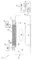
図1A及び図1Bは、本発明の原理によるプラズマ処理システムの一実施形態を示す。符号12で示す前記プラズマ処理システムは、図1A及び図1Bに概略的に示されている。プラズマ処理システム12は、プラズマ18を生成することができるプラズマ処理領域16を画定し、符号14で示すプラズマ処理チャンバを備える。チャックまたは電極22は、前記チャンバ14内に配置することができ、かつ処理領域16内において、チャンバ14内で基板20を支持するように構成されかつ配置されている。基板20は、半導体ウェハ、集積回路、被覆されるポリマー材からなるシート、イオン注入により表面硬化される金属、あるいは、例えば、エッチングまたは成膜される他の材料物質とすることができる。
1A and 1B illustrate one embodiment of a plasma processing system according to the principles of the present invention. The plasma processing system indicated by
図示してはいないが、例えば、チャンバ14に組み合わされた冷却供給流路を介して、冷却剤をチャック22に供給することができる。各冷却供給流路は、冷却供給源に結合することができる。例えば、前記冷却供給流路は、前記冷却供給源に、個別に接続することができる。別法として、冷却供給流路は、全ての冷却供給流路をあるパターンで接続する相互接続流路からなるネットワークによって相互接続することができる。
Although not shown, for example, the coolant can be supplied to the
概して、プラズマを生成するようにイオン化可能などのようなガスでもあり得るプラズマ生成ガスは、例えば、ガス注入口26を介してチャンバ14内に導入されてプラズマになる。前記プラズマ生成ガスは、当業者が理解しているように、所望の用途に従って選択することができ、例えば、窒素、キセノン、アルゴン、フルオロカーボン化学に対して四フッ化炭素(CF4)または八フッ化シクロブタン(C4F8)、塩素(Cl2)、臭化水素(HBr)、酸素(O2)、あるいは、他のガスとすることができる。
In general, a plasma generating gas, which can be any gas that can be ionized to generate a plasma, is introduced into the
ガス注入口26は、チャンバ14に結合されており、プラズマ処理ガスをプラズマ処理領域16内に導入するように構成されている。様々なガス注入口またはインジェクタ、および種々のガス注入動作を、プラズマ処理チャンバ14にプラズマ処理ガスを導入するのに用いることができ、前記チャンバは、密封することができ、またアルミニウムまたは他の適当な材質で形成することができる。プラズマ処理ガスは、ほとんどの場合、基板近くにまたは基板と反対側に配置されたガスインジェクタまたは注入口から導入される。例えば、図1A及び図1Bに示すように、ガス注入口26を介して供給されるガスは、容量結合型プラズマ(capacitively coupled plasma:CCP)源内の基板と対向する注入電極(上部電極28)を介して注入することができる。ガス注入口26を介して供給されるガスは、例えば、ガスフロー制御装置(図示せず)によって制御することができる。
The
別法として、図示しない実施形態においては、電磁結合型プラズマ(transformer coupled plasma:TCP)源内の基板と対向する誘電体窓を介して、ガスを注入することができる。図2から図6は、例えば、誘導結合型プラズマ(inductively coupled plasma:ICP)源内のガス注入プレートを介して、ガスを注入することができるプラズマ処理システム12の実施形態を示し、それらを以下に詳細に説明する。その他のガスインジェクタ構成が当業者に知られており、プラズマ処理チャンバ14と、例えば、ヘリコン(Helicon)及び電子サイクロトロン共鳴(electron cyclotron resonance:ECR)源等の他のプラズマ源と同様に、共に用いることができる。
Alternatively, in an embodiment not shown, the gas can be injected through a dielectric window facing a substrate in a source of electromagnetic coupled plasma (TCP). FIGS. 2-6 illustrate embodiments of a
プラズマ処理チャンバ14は、ポンピング装置33が取り付けられた排出口29を備えることができる。(図1Aの前記ポンピング装置に組み合わされたバルブ35として示す)ポンピング装置33内のスロットル制御バルブは、プラズマ処理チャンバ14内のガス圧力制御を実行することができる。ポンピング装置33は、ウェハ20の近傍からパーティクルを除去するように機能する。ゲートバルブ35及び真空ポンプ37(図1A)は、ポンピング装置33の構成要素であるが、簡略化のため、ポンピング装置33のみを、図2、図3、図4及び図6に示してある。
The
上部電極28及び下部電極(チャック)22の形として、プラズマ発生器は、プラズマ処理ガスをイオン化することによって、プラズマ処理領域16内にプラズマ18を生成するように、チャンバ14に結合することができる。前記プラズマ処理ガスは、例えば、上部電極28に結合された電源30を用いて、RFおよび/またはDC電力を前記ガスに供給することによってイオン化することができる。ある用途においては、前記プラズマ発生器は、例えば、RF電力を供給することが可能なアンテナまたはRFコイルを含んでもよい。例えば、電源30によってプラズマに供給される電力は、チャンバ14内に導入されるプラズマ生成ガス中で放電を引き起こすことができ、それによって、プラズマ18等のプラズマを生成することができる。
In the form of an
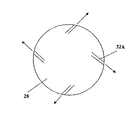
上部電極28は、その中に形成された1つ以上のガス注入路32A(図1A)または32B(図1B)を有することができる。注入路32A、32Bは、処理領域16に連通させることができ、かつガスインジェクタ26から離れた、パージガス(図示せず)、例えば不活性ガスの供給源からパージガスを供給することができる。ヘリウム、アルゴン、クリプトン、ネオン、キセノン及び他のガスまたは希ガス等の不活性ガスは、この目的のために使用することができる。ガス注入路32A、32Bは、いずれかの方向または角度で、チャンバ14の処理領域16内に入るように、上部電極28内に形成することができる。図1Aにおいて、ガス注入路32Aは、チャンバ14の内部チャンバ壁31に対して外側径方向に、パージガスの流れを注入するように構成されている。ガス注入路32Aは、内部チャンバ壁31と直角に、かつ基板20によって画定される面と平行にすることができる。注入路32Aは、パージガスの動きが、パージガスを、前記内部チャンバの概して周囲に流すことができるようにする遠心成分を有するように、あるいは、図1Cに示すように配置することができ、それにより、パーティクルが前記チャンバ壁にぶつかって流れ続け、かつ基板20から離れる。図1Cに示すように、注入路32Aは、例えば、直角ではない角度で内部チャンバ壁31を横切らせることができ、かつ基板20によって画定される面と平行にすることができる。
The
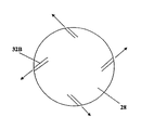
ガス注入路32Bは、注入されたパージガスが、上方または下方の動きの成分(下方の動き成分を示す図1B参照)を有し、かつ可能な限り渦巻形の成分(図1D参照)も有するように、内部チャンバ壁31に対して直角ではない角度で上部電極28内に形成することができる。図1Bにおいては、ガス注入路32Bは、基板20によって画定される面に対して直角にすることができ、図1Dにおいては、ガス注入路32Bは、基板20によって画定される面と平行にすることができる。これらの注入角度は、パーティクルを前記ウェハから離しておく前記チャンバ内でのフローパターンを生成することにより、ウェハ20からパーティクルを離しておくことを助ける。例えば、上記渦巻形の成分は、図1C及び図1Dに示すように、前記基板によって画定される面内に、注入路32A、32Bをある角度で向けることにより生成することができる。注入路32A、32Bは、電極28の半径に関する水平面に対してある角度で向けるように表すこともできる。別法として、注入路32A、32Bは、内部チャンバ壁31に対して直角にすることができ、例えば、内部チャンバ壁31に対して垂直ではない角度で向けることができる。
The
絶縁リング34は、上部電極28と、チャンバ14に結合されたDCまたはRFバイアス電極36とを実質的に囲むことができる。例えば、電極36は、絶縁リング34の外面に埋め込むことができる。
Insulating
DCまたはRFバイアス電極36は、適当な電源38によって起動することができる。電極36のパルシングは、ウェハ20の近傍からのパーティクルを、電極36の近傍に引き付けさせることができる。そこで、パージガスを、注入路32A、32Bを介して断続的または継続的に処理領域16に流して、パーティクルの流れをポンピング装置33に送ることができる。このようにして、パーティクルは、チャンバ14及び処理領域16から除去される。
The DC or
また、ガス注入路32A、32Bを介してパージガスを供給するのに加えて、パーティクルを引き付けるのに用いられるのとは異なる反対極性で(例えば、DCバイアスの場合)電極36をパルシングして、パーティクルを吹き飛ばすこと、例えば、ウェハ近傍からのパーティクルの除去をアシストすることも可能である。前記反対極性は、パーティクルの電極36への引き付けを終わらせ、ガス注入路32A、32Bを介して供給されるパージガスを用いたパーティクル除去を容易にする。
In addition to supplying the purge gas through the
様々なリード(図示せず)、例えば、電圧プローブまたは他のセンサを、プラズマ処理システム12に結合することができる。
Various leads (not shown), such as voltage probes or other sensors, can be coupled to the
プラズマ処理システム12への入力を伝え、かつ活性化させるのに十分な制御電圧を生成することが可能で、かつプラズマ処理システム12からの出力をモニタリングすることが可能なコントローラ(図示せず)を、プラズマ処理システム14に組み合わせることができる。例えば、前記コントローラは、上部電極28のRF電源30及びガス注入口26(または、前記注入口と流体的に連通する流量制御装置)に結合することができ、かつ前記電源及び前記制御装置と情報を交換することができる。さらに、前記コントローラは、図1A及び図1Bに示すように、それぞれ、ポンピング装置33及び電極36の電源38と連通させることができる。記憶装置に格納することができるプログラムを、格納されたプロセスレシピに従って、プラズマ処理システム12の上述した構成要素を制御するのに用いることができる。別法として、各コントローラが、例えば、プラズマ処理システム12の異なる構成要素を制御するように構成されている多数のコントローラを設けることができる。前記コントローラの1つの実例は、カリフォルニア州グレンデールのMicro/SYS社の組込み可能なPCコンピュータ型PC/104である。
A controller (not shown) capable of generating a control voltage sufficient to communicate and activate the input to the
図2は、図1A及び図1Bに示すプラズマ処理システム12と実質的に同様の構造及び動作からなるプラズマ処理システム112を示す。プラズマリアクタまたは発生器17が、容量結合型プラズマ(CCP)源、誘導結合型プラズマ(ICP)源、電磁結合型プラズマ(TCP)源、電子サイクロトロン共鳴(ECR)プラズマ源、ヘリコンプラズマ源または同様のシステムのうちのいずれかであってもよい「一般的な(generic)」プラズマリアクタを表わす。プラズマ処理システム112は、処理領域16と連通するように、チャンバ14の壁を貫通して形成されているガス注入路132を備える。ガス注入路132は、図2のチャンバ14の上壁に形成されているが、ガス注入路132は、前記チャンバまたはリアクタのいずれかの壁に、例えば、図1A及び図1Bの壁31に形成することができ、その結果、パージガスを、異なる方向または角度で、処理領域16に供給することができる。また、図2は、プラズマシステム112の側壁に取付けられた電極36を示す。異なるタイプのプラズマシステムまたはリアクタ、例えば、CCP、TCP、ヘリコンまたはECR型のシステムまたはリアクタにおいては、電極36は、そのようなタイプのシステムまたはリアクタのチャンバのいずれかの適当な壁に取付けることができる。
FIG. 2 shows a
電極36は、バイアスをかけて、ウェハ20の近傍からのパーティクルを、チャンバ14の外周部において、電極36の近傍に引き付けさせることができる。そこで、パージガスを、注入路132を介して処理領域16に流し、パーティクルの流れをポンピング装置33に送ることができる。このようにして、パーティクルは、チャンバ14及び処理領域16から除去される。
The
プラズマ処理システム12と同様に、プラズマ処理システム112は、ガス注入路32を介してパージガスを供給するのに加えて、パーティクルを引き付けるのに用いられるのとは異なる反対極性で(例えば、DCバイアスの場合)電極36をパルシングして、チャンバ14からパーティクルを除去することができる。
Similar to the
プラズマ処理システム12、112は、チャンバ14の処理領域16からパーティクルを除去するように、パージガスと共に、DCバイアスまたはRFバイアスを用いることが示される。図3に示されているプラズマ処理システム212は、チャンバ14の処理領域16からパーティクルを除去するようにパージガスのみを用いることが示される。プラズマ処理システム12、112の部材と、構造及び動作が実質的に等しいプラズマ処理システム212における同様の部材には、同じ参照数字を付けている。
The
プラズマ処理システム212は、チャック22、または、その上に前記チャックが位置するチャック台構造のいずれかに形成されているガス注入路232を含む。ガス注入路232は、ウェハ20から上方及び外側に、パージガスの流れを噴射するように構成されている。図3に示す実施形態においては、前記パージガスは、ガス注入路232を介して同時に供給することにより、前記ウェハ、特に前記ウェハの縁部からパーティクルを除去することができる。ガス注入路232は、上述したプラズマ処理システムまたはリアクタのいずれかに形成することができる。別法として、パージガスは、ガス注入路232を介して継続的に供給することができ、または、ガス注入路232を介して、異なる時間に供給することができる。
The
図4及び図5は、チャンバ14の処理領域16からパーティクルを除去するようにパージガスのみを用いることが、また、示されているプラズマ処理システム312を示す。システム12、112及び212の部材と、構造及び動作が実質的に等しいプラズマ処理システム312における同様の部材には、同じ参照数字を付けている。
FIGS. 4 and 5 show the
プラズマ処理システム312は、チャンバ14の周囲に配置されているガス注入路332(図5)を備えるパーティクル除去システムを含む。ガス注入路332は、パージガスの流れが、ウェハ20を越えた上方に向けられるように、チャンバ14の側壁に形成することができる。ガス注入路332は、セットまたはゾーンで作動することができ、その結果、1つのみのセットまたはゾーンが、一度にパルシングされる。例えば、図5において、各セットまたはゾーンは、4つまたは5つの注入路332を含むことができる。換言すれば、1つのセットまたはゾーンは、チャンバ14の周囲の約4分の1に及ぶが、異なる数のゾーン及びゾーンごとの注入路を用いてもよい。
The
1つのセットまたはゾーンの活性化(activation)は、ガスフロー及びパーティクルが、ウェハの中心近くに流れなくなることを避けることを可能にする。従って、パーティクルを、ウェハ20から吹き飛ばし、前記ウェハを横切ってウェハ20の他の側へ吹き飛ばして、ポンピング装置33を介して除去することができる。多数のセットまたはゾーンのガス注入路332を、例えば順次作動させることができ、その結果、各ガス注入路332が、少なくとも一度使用される。
Activation of one set or zone allows gas flow and particles to be prevented from flowing near the center of the wafer. Thus, particles can be blown away from the
図6は、チャンバ14の処理領域16からパーティクルを除去するようにパージガスのみを用いることが示されているプラズマ処理システム412を示す。システム12、112、212及び312の部材と、構造及び動作が実質的に等しいプラズマ処理システム412における同様の部材には、同じ参照数字を付けている。
FIG. 6 illustrates a
プラズマ処理システム412は、図6に示すように、展開渦リング構造402(expanding vortex ring structure 402)を生成して、チャンバ14の処理領域16からのパーティクルの除去を容易にするように構成されているガス注入路432を含む。
The
注入路432を介して、パルス上にガスを注入すると、ガスフローの渦リング構造402が生成され、これは、徐々に径方向に広がり、一定時間経過後に、(片方矢印で示す方向で)内部チャンバ壁31に到達し、パーティクルをウェハ20の上に浮遊させる。
When gas is injected over the pulse via the
プラズマ処理システムにおいては、パーティクルは、一般に、プラズマ18の静電力により、ウェハ20の上、特に、前記ウェハの縁部に浮遊する可能性がある。パーティクルは、概して、チャック22からRFバイアスを除去したとき、もしくはプラズマ18を消したときに、浮遊させていた静電電位が取り除かれ、ダメージを起こすパーティクルがウェハ20の上に積もり、デバイスに最もダメージを与える。上述した全ての実施形態において、ウェハの処理は、所定のレシピに従って実行することができ、プラズマ18が完全に消失する前に、プラズマ処理が本質的に停止している間、プラズマがまだ、パーティクルを浮遊させ続けるのに十分高密度である低RF電力動作を用いることができる。この低電力動作の間に、図1Aから図1D及び図2から図6に関して上述したプラズマ処理システム12、112、212、312、412を作動させて、チャンバ14の処理領域16からパーティクルを除去することができる。パーティクルが、ポンピング装置33を用いて、一旦、排出されると、RF電力及びプラズマは完全に消失する。また、ウェハの処理中に、図1Aから図1D及び図2から図6に関して上述したプラズマ処理システム12、112、212、312、412を作動させて、チャンバ14の処理領域16からパーティクルを除去することもできる。
In plasma processing systems, particles can generally float on the
図示していないが、図1Aから図1D及び図2から図6に関して上述したプラズマ処理システム12、112、212、312、412の特徴は、混合させることができる。より具体的には、注入路系32A、32B、132、232、332、432及び電極36は、いずれかの実施形態において置換することができる。例えば、プラズマ処理システム212において、(図2に示すプラズマ処理システム112に関して上述したように)電極36をチャンバ14の側壁に取付けて、チャック22の側部のガス注入路232を介してパージガスを供給することに加えて、電極36の近傍にパーティクルを引き付けることができる。
Although not shown, features of the
図7は、上述した実施形態のいずれかを用いて使用することができるプラズマ処理システムで基板を処理する方法を示す。図8から図11は、本発明の原理によるプラズマ処理システムでパーティクルを除去する種々の方法を示し、上述した特定の実施形態で実施することができる。 FIG. 7 illustrates a method for processing a substrate in a plasma processing system that can be used with any of the embodiments described above. FIGS. 8-11 illustrate various methods of removing particles in a plasma processing system according to the principles of the present invention and can be implemented in the particular embodiments described above.
図7に示すプラズマ処理システムで基板を処理する方法は、500で始まる。502において、ウェハが、前記プラズマ処理システムの処理領域内に配置される。504において、前記ウェハは、上述したような所定のプロセスレシピに従って処理される。ブロック506は、508においてパーティクルを除去することと、必要な場合に、510において、パーティクルの除去を繰り返すこととを含む、パーティクル除去シーケンスを規定する。ブロック506は、504のウェハ処理の後に続くが、前記パーティクル除去シーケンスは、ウェハが所定のプロセスレシピに従って処理されている間または処理された後に実行することができる。図8から図11は、ブロック506の代わりに、図7に示す上述した方法に代わりに用いることができる操作の実施例を示す。
The method of processing a substrate with the plasma processing system shown in FIG. At 502, a wafer is placed in a processing region of the plasma processing system. At 504, the wafer is processed according to a predetermined process recipe as described above.
508において、パーティクルは、少なくとも1つのパージガスと、プラズマ中の静電力とを用いて、前記処理チャンバの処理領域から除去される。パーティクルの除去は、必要に応じて、ウェハ処理の状況により繰り返すことができる(例えば、パーティクルがより発生しやすいプロセスの場合、多数のパーティクル除去操作を用いることができる)。このため、510において、前記パーティクル除去操作を繰り返すか否かの判断がなされる。そして、そのような場合、前記パーティクル除去操作は、508において繰り返され、新たな判断が、510においてなされる。除去操作の所定回数は、例えば、経験、実験、歩留まり及びダメージレベルに基づく所定回数を用いて決めることができる。 At 508, particles are removed from the processing region of the processing chamber using at least one purge gas and an electrostatic force in the plasma. Particle removal can be repeated as needed depending on the wafer processing situation (for example, in a process where particles are more likely to be generated, multiple particle removal operations can be used). Therefore, at 510, it is determined whether or not to repeat the particle removal operation. In such a case, the particle removal operation is repeated at 508 and a new determination is made at 510. The predetermined number of removal operations can be determined using a predetermined number based on experience, experiment, yield, and damage level, for example.
さらなるパーティクル除去操作が必要でない場合には、512において、ウェハを上記チャックに保持する電気バイアスが取り除かれる。514において、処理されたウェハは、上記プラズマ処理システムから移動される。516において、上記方法は終了する。 If no further particle removal operation is required, at 512, the electrical bias that holds the wafer to the chuck is removed. At 514, the processed wafer is moved from the plasma processing system. At 516, the method ends.
図8は、602において、パージガスをパルシングすることと、604において、必要に応じて前記パルシングを繰り返すこととを含む、パーティクル除去シーケンスを規定するブロック606を示す。ブロック606は、504において、上記基板が処理された後、または処理されている間に、602において、パージガスがパルシングされるように、ブロック506の代わりに、図7に示す上述した方法に代わりに用いることができる。604における判断が、604におけるパージガスのパルシングが必要であるという場合、前記パージガスは、602において、パルシングされる。604における判断が、前記パージガスのさらなるパルシングが必要でないという場合、シーケンス606は終了して、図7の512に続く。
FIG. 8 shows a
図9は、例えば、702において、DCまたはRFバイアスを、電極36等の電極に印加することを含むパーティクル除去シーケンスを規定するブロック706を示す。ブロック706のパーティクル除去シーケンスは、704において、パージガスをパルシングすることと、708において、必要に応じて前記バイアス及びガスのパルシングを繰り返すこととも含む。ブロック706は、DCまたはRFバイアスが、電極、例えば、図1から図2に示す電極36に印加されるように、ブロック506の代わりに、図7に示す上述した方法に代わりに用いることができる。708における判断が、さらなるパーティクル除去が必要であるという場合には、702において、DCまたはRFバイアスが印加され、704において、パージガスがパルシングされる。708における判断が、さらなるパーティクル除去が必要でないという場合には、シーケンス706は終了し、図7の512に続く。
FIG. 9 shows a
図10は、上記プラズマ処理チャンバの周囲に配置されている、ガス注入路の複数のノズルを介してパージガスを供給することを含むパーティクル除去シーケンスを規定するブロック806を示す。このパーティクル除去シーケンスは、例えば、図4及び図5に示すプラズマ処理システム312に用いることができる。ノズルの第1のセットは、802において、ガスを前記ノズルの第1のセットに供給するために、例えば、バルブまたは同様の装置を用いてガス供給装置に接続されており、804において、前記パージガスがパルシングされる。ノズルの追加的なセットを介したパージガスのパルシングが必要か否かの判断が、808においてなされる。必要な場合、810において、ノズルの前記追加的なセット、例えば、ノズルの第2のセットにガスを供給するために、例えば、バルブまたは同様の装置を用いて、パージガスの供給部を追加的なノズルに接続することができ、804におけるパージガスのパルシングが、前記ノズルの第2のまたは追加的なセットを用いて繰り返される。前記プロセスは、ノズルの全てのセットがパルシングされるまで繰り返される。前記ノズルセットは、どのような順序でもパルシングすることができ、前記シーケンスは、前記シーケンスの範囲内で、1つのセットを他のセットよりもより多くパルシングすることを含んでもよい。
FIG. 10 shows a
ブロック806は、504において、上記基板が処理された後に、上記プラズマ処理チャンバの周囲に配置されているガス注入路の複数のノズルを介して、パージガスが供給されるように、ブロック506の代わりに、図7に示す上述した方法に代わりに用いることができる。
図11は、900において、上記処理チャンバ内のパーティクル濃度を測定することと、902において、図8、図9または図10に示す方法のいずれかを用いて、前記チャンバ内のパーティクルを除去することとを含むパーティクル除去シーケンスを規定するブロック906を示す。パーティクル除去後に、904において、パーティクル濃度の新たな測定が実行される。パーティクル濃度の測定は、2002年11月26日に出願された、米国特許仮出願第60/429,067号の教示に従って実行することができ、前記出願の内容全体は参照してここに組み込まれる。別法として、公知のどのような方法も、パーティクル濃度を測定するのに用いてもよい。908において、パーティクル除去を繰り返すか否かの判断がなされる。そして、そのような場合、910において、(例えば、吸引力を変更する、除去を速めるため等)任意のものである、パーティクル除去条件(例えば、パージガス流量、DCまたはRF電極バイアスまたは他の条件)を変える必要があるか否かの判断がなされ、902において、前記除去操作が繰り返された後、新たなパーティクル濃度測定が、904において行われ、908において、繰り返しの新たな判断がなされる。一旦、最新の測定によってパーティクル濃度が安全なレベルまで低減されていることが確認されると、全てのRF電力が遮断され、(例えば、図7のフローチャートにおいて)上記ウェハが、上記処理チャンバから移動される。
FIG. 11 shows measuring the particle concentration in the processing chamber at 900 and removing particles in the chamber at 902 using any of the methods shown in FIG. 8, FIG. 9 or FIG. A
ブロック906は、504において、上記基板が処理され、900において、上記処理チャンバ内のパーティクル濃度が測定され、902において、前記チャンバ内のパーティクルが除去され、続いて、904において、新たなパーティクル濃度測定が行われるように、ブロック506の代わりに、図7の上述した方法に代わりに用いることができる。この最後に行われたパーティクル濃度測定は、統計的方法を用いて、図7のプロセス504の間のパーティクルによるダメージに関連付けることができる。一旦、許容可能なダメージレベルに達すると、測定されかつ関連付けられたパーティクル濃度を、他のプロセスのための目標値として用いることができる。他のプロセスの実行中には、910において、パラメータを調整することができ、あるいは、この目標の濃度が達成されるまで、ウェハにおける実際のダメージレベルを必ずしも算出することなく、ガスのパルシングの回数を繰り返す。この実際のダメージレベルを測定することの回避は、ウェハ処理実行中の時間を節約することができる。
上記方法は、プラズマ処理システム内のパーティクルを除去する上記の方法に加えて、プラズマ処理領域内のパーティクルを除去するための追加的な行為、操作または処理手順を含むことができる。それらの追加的な行為、操作または処理手順の様々な組合せを用いることもできる。例えば、上記プラズマ処理チャンバからパーティクルを除去する操作は、基板処理中に、または、基板が処理された後に、実行することができる。 In addition to the above method of removing particles in the plasma processing system, the method can include additional acts, operations, or processing procedures for removing particles in the plasma processing region. Various combinations of these additional acts, operations or processing procedures can also be used. For example, the operation of removing particles from the plasma processing chamber can be performed during substrate processing or after the substrate has been processed.
本発明を、その好適な実施形態に関して、具体的に示しかつ説明してきたが、当業者には、本発明の趣旨及び範囲を逸脱することなく、様々な形態及び詳細の変更が可能であることが理解されるであろう。 Although the invention has been particularly shown and described with respect to preferred embodiments thereof, various changes and modifications can be made by those skilled in the art without departing from the spirit and scope of the invention. Will be understood.
例えば、パーティクル測定装置を、図1A、図1B及び図2から図6に記載したプラズマ処理システム12、112、212、312または412のうちのいずれかと共に用いることができる。前記パーティクル測定装置は、チャンバ内のパーティクル濃度を読取るために、処理チャンバ14に結合することができる。パーティクル濃度データは、プラズマ処理システム12、112、212、312または412あるいはプラズマ処理チャンバ14が、例えば、クリーニングを要するとき及び場合を判断するのに用いることができる。従って、プラズマ処理システム12、112、212、312または412あるいはプラズマ処理チャンバ14は、必要な場合にのみクリーニングすることができ、このことは、典型的な歩留まりを改善することができ、かつプラズマ処理システム12、112、212、312または412の予防的なメンテナンスのための運転停止の頻度を減らすことができる。また、前記システムは、パーティクルの発生が極小化されるように、プロセスエンジニアが、プロセスパラメータを調整できるようにし、プロセスパラメータの調整が、ある特に不安定なプロセスに必要な場合、例えば、前記システムは、種々のプロセスレシピを比較することを可能にする測定値を提供する。
For example, a particle measuring device can be used with any of the
従って、上記の実施形態は、この発明の機能的なかつ構造上の原理を説明するために示しかつ記載されており、かつそれらの実施形態は、そのような原理から逸脱することなく、変更されることがある。そのため、この発明は、特許請求の範囲の趣旨及び範囲に含まれる全ての変更例を含む。 Accordingly, the foregoing embodiments have been shown and described to illustrate the functional and structural principles of the present invention, and the embodiments may be modified without departing from such principles. Sometimes. Therefore, the present invention includes all modifications included in the spirit and scope of the claims.
Claims (31)
前記チャンバ内の前記処理領域内に基板を支持するように構成されたチャックと、
前記チャンバと連通し、プラズマ処理の間、前記プラズマ処理領域にプラズマを生成するように構成されたプラズマ発生器と、
前記チャンバと連通する少なくとも1つのガス注入路とを具備し、
この少なくとも1つのガス注入路は、それを介してパージガスを流すことにより、前記チャンバからのパーティクルの除去を容易にするように構成されているプラズマ処理システム。 A chamber containing a plasma processing region;
A chuck configured to support a substrate in the processing region in the chamber;
A plasma generator in communication with the chamber and configured to generate plasma in the plasma processing region during plasma processing;
Comprising at least one gas injection path in communication with the chamber;
The plasma processing system, wherein the at least one gas injection path is configured to facilitate removal of particles from the chamber by flowing a purge gas therethrough.
この電極に、DCまたはRF電力でバイアスがかけられた場合に、静電力により、前記チャンバ内のパーティクルを引き付けるかまたははね返すように構成されている請求項1に記載のプラズマ処理システム。 Further comprising an electrode,
The plasma processing system of claim 1, wherein the electrode is biased or repelled by electrostatic force when the electrode is biased with DC or RF power.
前記電極は、パーティクルを前記チャンバから除去するように前記ガス注入路がパージガスを供給し得るように、パーティクル引き付けるようにバイアスがかけられ、その後、パーティクルの引き付けを終了させるようにバイアスがかけられる請求項3に記載のプラズマ処理システム。 When finishing attracting particles to the electrode,
The electrode is biased to attract particles so that the gas injection path can supply purge gas so as to remove particles from the chamber, and then biased to finish attracting particles. Item 4. The plasma processing system according to Item 3.
チャンバ内のパーティクルを除去することを具備し、
前記チャンバ内のパーティクルを除去することは、前記チャンバと連通する少なくとも1つのガス注入路を介してパージガスを供給することを含んでいる方法。 A method of processing a substrate in a plasma processing system having a chamber that includes a plasma processing region in which plasma can be generated during plasma processing to process the substrate, comprising:
Removing particles in the chamber,
Removing the particles in the chamber includes supplying a purge gas through at least one gas injection path in communication with the chamber.
前記少なくとも1つのガス注入路を介してパージガスを連続して供給することを含んでいる請求項23に記載の方法。 Removing the particles
24. The method of claim 23, comprising continuously supplying a purge gas through the at least one gas injection path.
前記チャンバの周辺に配置された複数のガス注入路を介してパージガスを供給することを含み、
各注入路は、パージガスを前記チャンバに注入するノズルを有している請求項23に記載の方法。 Removing the particles
Supplying a purge gas through a plurality of gas injection paths disposed around the chamber;
24. The method of claim 23, wherein each injection path has a nozzle for injecting a purge gas into the chamber.
前記注入路の第1のセットの各ノズルが、パージガスを前記チャンバに注入するように、前記複数のガス注入路の第1のセットを介してパージガスを供給することと、
前記注入路の第1のセットとは異なる時間に、前記注入路の第2のセットの各ノズルが、パージガスを前記チャンバに注入するように、前記複数のガス注入路の第2のセットを介してパージガスを供給することとをさらに含んでいる請求項23に記載の方法。 Removing the particles
Supplying a purge gas through the first set of gas injection paths such that each nozzle of the first set of injection paths injects a purge gas into the chamber;
Through a second set of gas injection paths, each nozzle of the second set of injection paths injects a purge gas into the chamber at a different time than the first set of injection paths. 24. The method of claim 23, further comprising: supplying a purge gas.
パーティクル測定装置を用いて、前記チャンバ内のパーティクル濃度を測定することと、
前記測定したパーティクル濃度に基づいて、前記チャンバ内のパーティクルを除去することを繰り返すこととをさらに含んでいる請求項23に記載の方法。 Removing the particles
Using a particle measuring device to measure the particle concentration in the chamber;
24. The method of claim 23, further comprising repeating removing particles in the chamber based on the measured particle concentration.
前記チャンバ内のパーティクルを引き付けるかまたははね返すように構成された電極に電圧を印加することを含んでいる請求項23に記載の方法。 Removing the particles
24. The method of claim 23, comprising applying a voltage to an electrode configured to attract or bounce particles in the chamber.
前記チャンバから引き付けたパーティクルを除去するように、前記パージガスを供給することとをさらに具備する請求項23に記載の方法。 Applying a voltage to an electrode configured to attract particles in the chamber from the substrate toward the electrode;
24. The method of claim 23, further comprising supplying the purge gas so as to remove particles attracted from the chamber.
前記チャンバから前記パーティクルを除去するように、前記パージガスを供給することとをさらに具備する請求項29に記載の方法。 Applying a voltage to the electrode so as to finish attracting particles in the chamber toward the electrode;
30. The method of claim 29, further comprising supplying the purge gas to remove the particles from the chamber.
Applications Claiming Priority (2)
| Application Number | Priority Date | Filing Date | Title |
|---|---|---|---|
| US45843203P | 2003-03-31 | 2003-03-31 | |
| PCT/US2004/001406 WO2004095502A2 (en) | 2003-03-31 | 2004-01-21 | Plasma processing system and method |
Publications (1)
| Publication Number | Publication Date |
|---|---|
| JP2006524914A true JP2006524914A (en) | 2006-11-02 |
Family
ID=33310684
Family Applications (1)
| Application Number | Title | Priority Date | Filing Date |
|---|---|---|---|
| JP2006508616A Withdrawn JP2006524914A (en) | 2003-03-31 | 2004-01-21 | Plasma processing system and method |
Country Status (3)
| Country | Link |
|---|---|
| US (1) | US20060060303A1 (en) |
| JP (1) | JP2006524914A (en) |
| WO (1) | WO2004095502A2 (en) |
Cited By (2)
| Publication number | Priority date | Publication date | Assignee | Title |
|---|---|---|---|---|
| CN104465292A (en) * | 2014-11-28 | 2015-03-25 | 上海华力微电子有限公司 | Pretreatment method for ion implanter |
| KR20220104667A (en) * | 2014-06-10 | 2022-07-26 | 램 리써치 코포레이션 | Defect control and stability of dc bias in rf plasma-based substrate processing systems using molecular reactive purge gas |
Families Citing this family (28)
| Publication number | Priority date | Publication date | Assignee | Title |
|---|---|---|---|---|
| US8349128B2 (en) | 2004-06-30 | 2013-01-08 | Applied Materials, Inc. | Method and apparatus for stable plasma processing |
| US20060000802A1 (en) * | 2004-06-30 | 2006-01-05 | Ajay Kumar | Method and apparatus for photomask plasma etching |
| KR100672820B1 (en) * | 2004-11-12 | 2007-01-22 | 삼성전자주식회사 | Method of processing a processed object using plasma |
| US20060130966A1 (en) * | 2004-12-20 | 2006-06-22 | Darko Babic | Method and system for flowing a supercritical fluid in a high pressure processing system |
| US7572737B1 (en) * | 2006-06-30 | 2009-08-11 | Lam Research Corporation | Apparatus and methods for adjusting an edge ring potential substrate processing |
| JP4916802B2 (en) * | 2006-07-20 | 2012-04-18 | 大日本スクリーン製造株式会社 | Heat treatment equipment |
| US7943005B2 (en) | 2006-10-30 | 2011-05-17 | Applied Materials, Inc. | Method and apparatus for photomask plasma etching |
| US7909961B2 (en) * | 2006-10-30 | 2011-03-22 | Applied Materials, Inc. | Method and apparatus for photomask plasma etching |
| KR101437522B1 (en) * | 2007-09-05 | 2014-09-03 | 어플라이드 머티어리얼스, 인코포레이티드 | Cathode liner with wafer edge gas injection in a plasma reactor chamber |
| US7832354B2 (en) * | 2007-09-05 | 2010-11-16 | Applied Materials, Inc. | Cathode liner with wafer edge gas injection in a plasma reactor chamber |
| US7879250B2 (en) | 2007-09-05 | 2011-02-01 | Applied Materials, Inc. | Method of processing a workpiece in a plasma reactor with independent wafer edge process gas injection |
| US20090086400A1 (en) * | 2007-09-28 | 2009-04-02 | Intevac, Inc. | Electrostatic chuck apparatus |
| US20090222804A1 (en) * | 2008-02-29 | 2009-09-03 | Illinois Tool Works, Inc. | Embedded firmware updating system and method |
| US20110011534A1 (en) * | 2009-07-17 | 2011-01-20 | Rajinder Dhindsa | Apparatus for adjusting an edge ring potential during substrate processing |
| JP5397215B2 (en) * | 2009-12-25 | 2014-01-22 | ソニー株式会社 | Semiconductor manufacturing apparatus, semiconductor device manufacturing method, simulation apparatus, and simulation program |
| US8664563B2 (en) * | 2011-01-11 | 2014-03-04 | Gas Technology Institute | Purging and debris removal from holes |
| US9228261B2 (en) * | 2011-08-02 | 2016-01-05 | Tokyo Electron Limited | System and method for tissue construction using an electric field applicator |
| CN102856150B (en) * | 2012-09-29 | 2015-08-26 | 中微半导体设备(上海)有限公司 | Plasm reaction cavity cleaning device and plasm reaction cavity cleaning method thereof |
| CN103839745B (en) * | 2012-11-23 | 2016-06-22 | 中微半导体设备(上海)有限公司 | A kind of swing plasm restraint device |
| US20150247238A1 (en) * | 2014-03-03 | 2015-09-03 | Lam Research Corporation | Rf cycle purging to reduce surface roughness in metal oxide and metal nitride films |
| US9478408B2 (en) | 2014-06-06 | 2016-10-25 | Lam Research Corporation | Systems and methods for removing particles from a substrate processing chamber using RF plasma cycling and purging |
| US10081869B2 (en) | 2014-06-10 | 2018-09-25 | Lam Research Corporation | Defect control in RF plasma substrate processing systems using DC bias voltage during movement of substrates |
| JP2017096827A (en) * | 2015-11-26 | 2017-06-01 | 東京エレクトロン株式会社 | Particle concentration mechanism, particle measurement device, and substrate processing device equipped with particle measurement device |
| JP6569521B2 (en) * | 2015-12-24 | 2019-09-04 | 東京エレクトロン株式会社 | Deposition equipment |
| US10413913B2 (en) | 2017-02-15 | 2019-09-17 | Tokyo Electron Limited | Methods and systems for dielectrophoresis (DEP) separation |
| CN112789718A (en) | 2018-10-01 | 2021-05-11 | 东京毅力科创株式会社 | Device and method for removing foreign matters on surface of substrate by static electricity |
| WO2020112923A1 (en) * | 2018-11-30 | 2020-06-04 | Lam Research Corporation | Throughput improvement with interval conditioning purging |
| KR20230169722A (en) * | 2022-06-09 | 2023-12-18 | 주식회사 나이스플라즈마 | Plasma chamber forming swirl motion with side gas feed |
Family Cites Families (7)
| Publication number | Priority date | Publication date | Assignee | Title |
|---|---|---|---|---|
| US5102496A (en) * | 1989-09-26 | 1992-04-07 | Applied Materials, Inc. | Particulate contamination prevention using low power plasma |
| JP3137682B2 (en) * | 1991-08-12 | 2001-02-26 | 株式会社日立製作所 | Method for manufacturing semiconductor device |
| US5522934A (en) * | 1994-04-26 | 1996-06-04 | Tokyo Electron Limited | Plasma processing apparatus using vertical gas inlets one on top of another |
| US5573597A (en) * | 1995-06-07 | 1996-11-12 | Sony Corporation | Plasma processing system with reduced particle contamination |
| US5854138A (en) * | 1997-07-29 | 1998-12-29 | Cypress Semiconductor Corp. | Reduced-particle method of processing a semiconductor and/or integrated circuit |
| US6486081B1 (en) * | 1998-11-13 | 2002-11-26 | Applied Materials, Inc. | Gas distribution system for a CVD processing chamber |
| WO2001001467A1 (en) * | 1999-06-29 | 2001-01-04 | Tohoku Techno Arch Co., Ltd. | Method and apparatus for processing fine particle dust in plasma |
-
2004
- 2004-01-21 WO PCT/US2004/001406 patent/WO2004095502A2/en active Application Filing
- 2004-01-21 JP JP2006508616A patent/JP2006524914A/en not_active Withdrawn
-
2005
- 2005-09-28 US US11/236,535 patent/US20060060303A1/en not_active Abandoned
Cited By (4)
| Publication number | Priority date | Publication date | Assignee | Title |
|---|---|---|---|---|
| KR20220104667A (en) * | 2014-06-10 | 2022-07-26 | 램 리써치 코포레이션 | Defect control and stability of dc bias in rf plasma-based substrate processing systems using molecular reactive purge gas |
| KR102576851B1 (en) * | 2014-06-10 | 2023-09-08 | 램 리써치 코포레이션 | Defect control and stability of dc bias in rf plasma-based substrate processing systems using molecular reactive purge gas |
| CN104465292A (en) * | 2014-11-28 | 2015-03-25 | 上海华力微电子有限公司 | Pretreatment method for ion implanter |
| CN104465292B (en) * | 2014-11-28 | 2017-05-03 | 上海华力微电子有限公司 | Pretreatment method for ion implanter |
Also Published As
| Publication number | Publication date |
|---|---|
| US20060060303A1 (en) | 2006-03-23 |
| WO2004095502A2 (en) | 2004-11-04 |
| WO2004095502A3 (en) | 2005-06-09 |
Similar Documents
| Publication | Publication Date | Title |
|---|---|---|
| JP2006524914A (en) | Plasma processing system and method | |
| TWI710415B (en) | Methods for eliminating fluorine residue in a substrate processing chamber using a plasma-based process | |
| US9735021B2 (en) | Etching method | |
| JP5185251B2 (en) | Gas injection system with reduced contamination and method of use thereof | |
| US9455133B2 (en) | Hollow cathode device and method for using the device to control the uniformity of a plasma process | |
| JP4388020B2 (en) | Semiconductor plasma processing apparatus and method | |
| US9793134B2 (en) | Etching method | |
| US20070227663A1 (en) | Substrate processing apparatus and side wall component | |
| US20180311707A1 (en) | In situ clean using high vapor pressure aerosols | |
| US9818582B2 (en) | Plasma processing method | |
| CN113257653A (en) | Mounting table, plasma processing apparatus, and cleaning method | |
| US9735025B2 (en) | Etching method | |
| US20060289296A1 (en) | Plasma processing method and high-rate plasma etching apparatus | |
| JP2009238837A (en) | Plasma processing apparatus and method | |
| US7744720B2 (en) | Suppressor of hollow cathode discharge in a shower head fluid distribution system | |
| US11501976B2 (en) | Substrate processing method and substrate processing apparatus | |
| KR20080014938A (en) | Apparatus for removing particle of electro static chuck | |
| JP2007266522A (en) | Plasma treatment device and processing method employing it | |
| KR100837625B1 (en) | A method and apparatus for treating substrates | |
| JP2004134437A (en) | Method and apparatus for manufacturing semiconductor device | |
| JP2004335637A (en) | Etching method and etching device | |
| KR100360177B1 (en) | Method for controlling an etching process of semiconductor | |
| KR100715012B1 (en) | Gas discharge suppressing member and plasma processing apparatus | |
| TW202226327A (en) | Plasma processing device and processing method thereof characterized by adding the gas supplying sources connected to the gas channel and using the valve to control the kind and flow of the supplied gas, thereby flexibly switching gas supply on demand during substrate processing and chamber cleaning | |
| KR20050100866A (en) | Dry etching device of semiconductor manufacture device |
Legal Events
| Date | Code | Title | Description |
|---|---|---|---|
| A621 | Written request for application examination |
Free format text: JAPANESE INTERMEDIATE CODE: A621 Effective date: 20061129 |
|
| A761 | Written withdrawal of application |
Free format text: JAPANESE INTERMEDIATE CODE: A761 Effective date: 20071010 |