JP2006332694A - Method for forming metal bumps on semiconductor surface - Google Patents
Method for forming metal bumps on semiconductor surface Download PDFInfo
- Publication number
- JP2006332694A JP2006332694A JP2006200592A JP2006200592A JP2006332694A JP 2006332694 A JP2006332694 A JP 2006332694A JP 2006200592 A JP2006200592 A JP 2006200592A JP 2006200592 A JP2006200592 A JP 2006200592A JP 2006332694 A JP2006332694 A JP 2006332694A
- Authority
- JP
- Japan
- Prior art keywords
- layer
- metal
- pillar
- solder
- depositing
- Prior art date
- Legal status (The legal status is an assumption and is not a legal conclusion. Google has not performed a legal analysis and makes no representation as to the accuracy of the status listed.)
- Pending
Links
Images


Classifications
-
- H—ELECTRICITY
- H01—ELECTRIC ELEMENTS
- H01L—SEMICONDUCTOR DEVICES NOT COVERED BY CLASS H10
- H01L24/00—Arrangements for connecting or disconnecting semiconductor or solid-state bodies; Methods or apparatus related thereto
- H01L24/01—Means for bonding being attached to, or being formed on, the surface to be connected, e.g. chip-to-package, die-attach, "first-level" interconnects; Manufacturing methods related thereto
- H01L24/10—Bump connectors ; Manufacturing methods related thereto
- H01L24/11—Manufacturing methods
-
- H—ELECTRICITY
- H01—ELECTRIC ELEMENTS
- H01L—SEMICONDUCTOR DEVICES NOT COVERED BY CLASS H10
- H01L2224/00—Indexing scheme for arrangements for connecting or disconnecting semiconductor or solid-state bodies and methods related thereto as covered by H01L24/00
- H01L2224/01—Means for bonding being attached to, or being formed on, the surface to be connected, e.g. chip-to-package, die-attach, "first-level" interconnects; Manufacturing methods related thereto
- H01L2224/10—Bump connectors; Manufacturing methods related thereto
- H01L2224/11—Manufacturing methods
- H01L2224/1147—Manufacturing methods using a lift-off mask
-
- H—ELECTRICITY
- H01—ELECTRIC ELEMENTS
- H01L—SEMICONDUCTOR DEVICES NOT COVERED BY CLASS H10
- H01L2224/00—Indexing scheme for arrangements for connecting or disconnecting semiconductor or solid-state bodies and methods related thereto as covered by H01L24/00
- H01L2224/01—Means for bonding being attached to, or being formed on, the surface to be connected, e.g. chip-to-package, die-attach, "first-level" interconnects; Manufacturing methods related thereto
- H01L2224/10—Bump connectors; Manufacturing methods related thereto
- H01L2224/11—Manufacturing methods
- H01L2224/119—Methods of manufacturing bump connectors involving a specific sequence of method steps
- H01L2224/11901—Methods of manufacturing bump connectors involving a specific sequence of method steps with repetition of the same manufacturing step
- H01L2224/11902—Multiple masking steps
-
- H—ELECTRICITY
- H01—ELECTRIC ELEMENTS
- H01L—SEMICONDUCTOR DEVICES NOT COVERED BY CLASS H10
- H01L2924/00—Indexing scheme for arrangements or methods for connecting or disconnecting semiconductor or solid-state bodies as covered by H01L24/00
- H01L2924/013—Alloys
- H01L2924/014—Solder alloys
-
- H—ELECTRICITY
- H01—ELECTRIC ELEMENTS
- H01L—SEMICONDUCTOR DEVICES NOT COVERED BY CLASS H10
- H01L2924/00—Indexing scheme for arrangements or methods for connecting or disconnecting semiconductor or solid-state bodies as covered by H01L24/00
- H01L2924/10—Details of semiconductor or other solid state devices to be connected
- H01L2924/11—Device type
- H01L2924/14—Integrated circuits
-
- H—ELECTRICITY
- H01—ELECTRIC ELEMENTS
- H01L—SEMICONDUCTOR DEVICES NOT COVERED BY CLASS H10
- H01L2924/00—Indexing scheme for arrangements or methods for connecting or disconnecting semiconductor or solid-state bodies as covered by H01L24/00
- H01L2924/15—Details of package parts other than the semiconductor or other solid state devices to be connected
- H01L2924/151—Die mounting substrate
- H01L2924/156—Material
- H01L2924/15786—Material with a principal constituent of the material being a non metallic, non metalloid inorganic material
- H01L2924/15787—Ceramics, e.g. crystalline carbides, nitrides or oxides
-
- H—ELECTRICITY
- H01—ELECTRIC ELEMENTS
- H01L—SEMICONDUCTOR DEVICES NOT COVERED BY CLASS H10
- H01L2924/00—Indexing scheme for arrangements or methods for connecting or disconnecting semiconductor or solid-state bodies as covered by H01L24/00
- H01L2924/30—Technical effects
- H01L2924/35—Mechanical effects
- H01L2924/351—Thermal stress
Abstract
Description
発明の属する技術分野
本発明は集積回路素子の製造に関し、さらに詳細には、信頼性の高い微細ピッチのはんだバンプを低コストで作製する方法に関する。
BACKGROUND OF THE INVENTION 1. Field of the Invention The present invention relates to the manufacture of integrated circuit elements, and more particularly, to a method for producing a highly reliable fine pitch solder bump at a low cost.
従来の技術
半導体素子の実装については、長年にわたって、半導体素子の機能サイズのさらなる減少(素子性能の向上と素子製造コストの減少という二重の要件によって促される)に重点が置かれている。こうした傾向に基づいて半導体素子密度の大幅な増大がもたらされており、素子またはパッケージのI/O能力に益々重点が置かれるようになっている。従って、集積回路と他の回路もしくはシステム部品とを接続する金属接続物がより一層重要になってきており、半導体素子のさらなる小型化と相俟って、回路の性能に対して益々好ましくない影響を及ぼすようになっている。金属相互接続物の寄生容量と抵抗が増大すると、チップの性能が大幅に低下することがある。この点に関して最も重要なのは、電源バス(power bus)もしくは接地バス(ground bus)に沿っての電圧低下、および臨界信号路(critical signal paths)のRC遅延である。より幅広の金属線を使用することによって抵抗を少なくしようとすると、これら金属線の容量がより高くなる。
Prior Art Semiconductor device packaging has been focused on the further reduction in the functional size of semiconductor devices (promoted by the dual requirement of improved device performance and reduced device manufacturing costs) over the years. This trend has led to a significant increase in semiconductor device density, with increasing emphasis on the I / O capability of the device or package. Therefore, metal connections that connect an integrated circuit with other circuits or system components are becoming more important, and coupled with further miniaturization of semiconductor elements, an increasingly unfavorable impact on circuit performance. It has come to exert. As parasitic capacitance and resistance of metal interconnects increase, chip performance can be significantly degraded. Most important in this regard is the voltage drop along the power or ground bus and the RC delay of the critical signal paths. If the resistance is reduced by using wider metal lines, the capacity of these metal lines will be higher.
こうした実装上の問題を解決するためにとられているアプローチの1つは、相互接続ワイヤ用に低抵抗の金属(たとえば銅)を開発することであるが、信号線間に低誘電率の材料が使用されている。I/O能力の問題を解決するための他のアプローチは、適切な製造コストでチップを相互接続する高信頼性の方法をもたらすようなチップ実装技術を設計することである。こうしたことからフリップ・チップ・パッケージが開発された。 One approach taken to solve these packaging problems is to develop a low resistance metal (eg, copper) for the interconnect wires, but with a low dielectric constant material between the signal lines Is used. Another approach to solving the I / O capability problem is to design a chip mounting technology that provides a reliable way to interconnect the chips at a reasonable manufacturing cost. For this reason, flip chip packages were developed.
フリップ・チップ技術により、チップのAlパッド上にバンプ(一般にはPb/Snはんだ)が作製され、パッケージ媒体(package media)(通常は、セラミックまたはプラスチックをベースとしている)にパンプが直接相互接続される。フリップ・チップは、最短路を介して、表を下にしてパッケージ媒体に接合される。これらの技術は、単一チップの実装だけでなく、複数チップ又は集積されたレベルの実装(パッケージがより大きい)にも、および幾つかのチップを収容してより大きな機能ユニットを形成するより高度な基板にも適用することができる。 Flip chip technology creates bumps (typically Pb / Sn solder) on the Al pads of the chip and interconnects the bumps directly to the package media (usually based on ceramic or plastic). The The flip chip is bonded to the package medium face down through the shortest path. These technologies are not only for single-chip implementations, but also for multiple-chip or integrated level implementations (larger packages) and more sophisticated to accommodate several chips to form larger functional units It can be applied to any substrate.
いろいろなI/O相互接続物を使用するフリップ・チップ技術は、パッケージに対する極めて低いインダクタンスの相互接続と相俟って、素子への最も高い密度の相互接続を達成するという利点を有する。しかしながら、予備試験可能性(pre−testability)、接合後の目視検査、およびはんだバンプの疲労を防止するための熱膨張係数(CTE)の整合などが、まだ課題として残っている。幾つかのパッケージを一緒に実装する場合(たとえば、プラスチック基板へのセラミックパッケージの表面実装など)、CTEが不整合であると、はんだ−鉛接合部に対して大きな熱応力を引き起こすことがあり、従って温度サイクル操作によるはんだ疲労によって接合部の破壊が起こることがある。 Flip chip technology using various I / O interconnects has the advantage of achieving the highest density interconnect to the device, coupled with the very low inductance interconnect to the package. However, pre-testability, visual inspection after joining, and thermal expansion coefficient (CTE) matching to prevent fatigue of the solder bumps still remain issues. When mounting several packages together (for example, surface mounting a ceramic package on a plastic substrate), mismatched CTEs can cause significant thermal stress on the solder-lead joint, Therefore, the joint may be destroyed by solder fatigue due to temperature cycle operation.
従来技術の基板実装は、セラミックとプラスチックのフリップ・チップ実装を使用する。セラミック基板の実装は高コストであり、全体としてのパッケージの性能を制約することがわかっている。最近では、プラスチック基板のフリップ・チップ実装が見られるようになり、このタイプの実装が設計の大きな流れとなっていて、大量のフリップ・チップ・パッケージの製造においてしばしば使用されている。プラスチック基板のフリップ・チップ・パッケージは、低密度のフリップ・チップ集積回路(IC)に使用されると充分に機能を果たす。ICから出ているピンの数が多い場合(すなわち350ピンを越える場合)、あるいはICから出ているピンの数が350ピンより少ないが、必要とされる全体としてのパッケージサイズが小さい場合、プラスチックのフリップ・チップ構造物は複雑かつ高コストになる。このことは、プラスチックのフリップ・チップ・パッケージを製造するのに使用される多層構造物に対してトレースすることができる。この多層構造物を使用すると、一般には2〜3ミルの範囲のパッケージ線密度が得られる。この線密度は、単層内のパッケージに対してチップI/Oからはんだボールまでファンアウト(fan out)を達成するには充分とは言えず、従って多層アプローチが求められることになる。多層アプローチは比較的厚い(50〜75μm)誘電体層を使用し、これらの層は、プラスチックのフリップ・チップ・パッケージが実装されるラミネート基板の熱膨張係数(CTE)よりかなり高いCTEを有する。こうしたCTEの差を和らげるために、全体としてのパッケージを(熱的および機械的に)バランスさせなければならず、従ってさらなる材料と、これらの材料を施すためのさらなるプロセス工程が使用され、このためボール・グリッド・アレイ(Ball Grid Array)パッケージのコストが増し、いろいろ問題が生じる。 Prior art substrate mounting uses ceramic and plastic flip chip mounting. Mounting ceramic substrates has been found to be costly and limit the overall package performance. Recently, flip-chip mounting of plastic substrates has become commonplace, and this type of mounting has become a major design trend and is often used in the manufacture of large numbers of flip chip packages. Plastic substrate flip chip packages perform well when used in low density flip chip integrated circuits (ICs). If the number of pins coming out of the IC is large (ie more than 350 pins) or the number of pins coming out of the IC is less than 350 pins but the overall package size required is small, plastic This flip chip structure is complex and expensive. This can be traced to a multilayer structure used to manufacture plastic flip chip packages. When this multilayer structure is used, a package line density in the range of 2-3 mils is generally obtained. This linear density is not sufficient to achieve a fan out from chip I / O to solder balls for a package in a single layer, thus requiring a multi-layer approach. The multilayer approach uses relatively thick (50-75 μm) dielectric layers that have a CTE that is significantly higher than the coefficient of thermal expansion (CTE) of the laminate substrate on which the plastic flip chip package is mounted. To alleviate these CTE differences, the overall package must be balanced (thermally and mechanically), so additional materials and additional process steps for applying these materials are used, and thus The cost of a ball grid array package increases, and various problems arise.
半導体素子を製造する上での、素子と素子機能(device features)とを相互接続する技術が、今日のようなサブミクロン素子の時代においても依然として続いている課題である。こうした目的に対してボンドパッドとはんだバンプがしばしば使用されており、従って、単純で、信頼性が高くて、そして低コストのボンドパッドとはんだバンプを製造することに継続的な努力が注がれている。 The technology for interconnecting devices and device features in the manufacture of semiconductor devices remains a challenge that continues in the era of submicron devices such as today. Bond pads and solder bumps are often used for these purposes, and therefore, continuous efforts are made to produce simple, reliable, and low cost bond pads and solder bumps. ing.
ボンドパッドは一般に、素子エレメントを結びつけるために、またダイの露出接点区域をもたらすために使用される。これらの接点区域は、ダイに対して外部の部品にダイを結びつけるのに適切である。たとえば、ボンドワイヤの一端が半導体ダイのボンドパッドに結びつけられ、そしてボンドワイヤの他端がプリント回路基板の一部に結びつけられる。従来技術に対しては、ボンドパッドの信頼性を高めつつ製造プロセスが単純化できるような、ボンドパッドの製造面での改良が絶えず求められている。 Bond pads are generally used to tie element elements and to provide exposed contact areas for the die. These contact areas are suitable to tie the die to parts external to the die. For example, one end of the bond wire is tied to the bond pad of the semiconductor die and the other end of the bond wire is tied to a portion of the printed circuit board. There is a continuing need for prior art improvements in bond pad manufacturing that can simplify the manufacturing process while increasing bond pad reliability.
ボンドパッドに一般的に使用される材料としては、タングステンやアルミニウム等の金属材料があるが、ドーピング量の多いポリシリコンも材料を接触させるのに使用することができる。ボンドパッドは半導体素子の上表面に形成され、このとき導電性材料が絶縁性の誘電体層中に埋め込まれることが多い。ポリシリコンをボンドパッド材料として使用する場合、N−領域と接触させるためのn−型ドーパントをポリシリコンにドーピングすることができるが、P−領域と接触させるためのp−型ドーパントをポリシリコンにドーピングすることもできる。こうしたドーピングというアプローチにより、ドーパントの相互拡散とマイグレーションが防止される。ボンドパッドのエリアに対しては低い接触抵抗が必要とされるが、湿気や化学溶媒の吸収の防止、薄いフィルムの接着特性、離層、および亀裂についての検討がボンドパッドの作製に対しては重要である。 Commonly used materials for bond pads include metallic materials such as tungsten and aluminum, but polysilicon with a high amount of doping can also be used to contact the material. The bond pad is formed on the upper surface of the semiconductor element, and at this time, a conductive material is often embedded in an insulating dielectric layer. If polysilicon is used as the bond pad material, the polysilicon can be doped with an n-type dopant for contact with the N-region, but a p-type dopant for contact with the P-region may be added to the polysilicon. It can also be doped. This doping approach prevents dopant interdiffusion and migration. Low contact resistance is required for the bond pad area, but consideration of moisture and chemical solvent absorption, thin film adhesive properties, delamination, and cracks is important for bond pad fabrication. is important.
アルミニウムボンドパッドを作製するのに使用される従来の加工シーケンスは、半導体表面(一般にはシリコン単結晶基板の表面)からスタートする。半導体表面を覆うようにイントラメタル誘電体(Intra Metal Dielectric)(IMD)の層を付着させ、IMD層の表面を覆うように金属(一般にはアルミニウム)の層を付着させる。金属の層をパターン焼き付けし、一般にはフォトレジスト層および写真平板法とエッチカング法の従来法を使用してエッチングする。この方法でボンドパッドを作製した後、IMDの層を覆うようにパシベーション層を付着させる。再び写真平板法とエッチング法を使用して、ボンドパッドと整列した開口をパシベーション層中に作製する。 Conventional processing sequences used to make aluminum bond pads start from a semiconductor surface (generally the surface of a silicon single crystal substrate). A layer of Intra Metal Dielectric (IMD) is deposited over the semiconductor surface, and a layer of metal (generally aluminum) is deposited over the surface of the IMD layer. The metal layer is pattern baked and etched, typically using a photoresist layer and conventional methods of photolithographic and etch canng. After the bond pad is fabricated by this method, a passivation layer is deposited so as to cover the IMD layer. Using photolithography and etching again, openings aligned with the bond pads are made in the passivation layer.
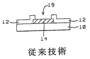
次に、導体パッド(contact pad)上にはんだバンプを作製するのに使用される従来法について説明する。図1〜4は、相互接続バンプを作製するのに使用される方法の1つの例をしている。半導体表面10に金属導体パッド14が設けられており、半導体表面10はパシベーション層12で保護されている。パシベーション層12に開口19が造られており、金属導体パッド14の表面が、この開口19を通して露出されている。図2では、パシベーション層12の表面を覆うように誘電体層16を付着させている。誘電体層16をパターン焼き付け及びエッチングし、これによって金属パッド14と整列していて、金属パッド14の表面を部分的に露出させる開口21を誘電体層16に作製する。一般にはアンダーバンプメタラージ(UBM)を使用して、誘電体層16を覆うように金属層18を作製し、このとき金属層18は、開口21の内部で金属パッド14の表面と接触している。金属パッド14の上に位置する金属層18の区域は、プロセシングにおける後の段階で、相互接続バンプが造られる台座(pedestal)を形成する。この台座はさらに、フォトレジストもしくは誘電体物質を含有する1つ以上の層の付着とパターン焼き付けによって垂直方向に延ばすことができる(これらの追加層は図2には示されていない)。これらの層は本質的に層16の形状を有しており、幾つかある最終的な加工工程のうちの、相互接続バンプの形成のために施される工程時において除去される。
Next, a conventional method used for producing solder bumps on a contact pad will be described. 1-4 illustrate one example of a method used to make interconnect bumps.
フォトレジスト層(図示せず)を付着させ、パターン焼き付けし、エッチングし、これによって導体パッド14と整列した開口を作製する。次いで、図3におけるたとえば銅やニッケルの金属層20(作製しようとする相互接続バンプの台座の一体部分を形成する)を、フォトレジスト層に作製された、また金属層18の表面上において作製された開口において電気メッキし、これによりメッキ工程時において層18が下側電極として機能する。従来技術での使用における層20は約1〜10μmの厚さを有しており、通常の厚さは約5μmである。最後に、層20の表面にはんだ層22を電気メッキする。次いで、パターン焼き付けされたフォトレジスト層を除去する。
A photoresist layer (not shown) is deposited, pattern baked, and etched, thereby creating openings aligned with the
金属層18をエッチングし(図4)、相互接続バンプのための台座のみを所定の場所に残す。このエッチングプロセス時に、付着させた層20と22がマスクとして機能する。前記のように、図2における台座のさらなる造形のために誘電体層またはフォトレジスト層の追加層が付着されている場合、これらの層もこの時点において除去される。
The
はんだペースト又ははんだフラックス(図示せず)をはんだ層22に施し、通常は窒素雰囲気下でリフロー表面にてはんだ22を溶融し、これにより球状の相互接続バンプ22(図4に示す)が作製される。
Solder paste or solder flux (not shown) is applied to the
相互接続バンプの台座をさらに造形するのに使用できる誘電体層またはフォトレジスト層の上記追加層の他に、相互接続バンプの作製を目的としている応用の多くは、バリヤー層として機能するか、あるいは他の特定の目的(たとえば、種々のオーバーレイ層の接着性の改良、または隣接層間の物質の拡散防止)を有する金属層を利用する。これらの層はまとまって図4の層18を形成し、上記から明らかなように、作製されるバンプの形状に対して影響を及ぼし、従ってしばしばボール・リミティング・メタル(Ball Limiting Metal)(BLM)層と呼ばれる。しばしば使用されるBLM層は、クロム、銅、および金の連続したオーバーレイ層であり、このときクロムは、下側に存在するアルミニウム導体パッドとの接着性を高めるのに使用されており、銅層は、下側層へのはんだ物質の拡散を防ぐよう機能しており、そして金層は、銅層の表面の酸化を防ぐよう機能している。BLM層は、図2〜4における層18である。
In addition to the above additional layers of dielectric or photoresist layers that can be used to further shape the interconnect bump pedestal, many of the applications aimed at making interconnect bumps function as barrier layers or Utilize metal layers with other specific purposes (eg, improving adhesion of various overlay layers, or preventing diffusion of materials between adjacent layers). These layers collectively form
素子密度を上げると、作製された半導体素子の一部である部品とエレメントの接近度が増す。こうした接近度の増大は、半導体素子のエレメント間のスペーシングまたは“ピッチ”の減少をもたらす。最先端の技術は約200μmのピッチを有するはんだバンプを使用し、素子密度のさらなる増大に対して制約を及ぼす。信頼性という点において、はんだバンプのピッチをさらに減少させる上で制約を受ける(従って、はんだバンプに対して比較的大きなボールサイズが要求されるということである)。このようにはんだボールが比較的大きいと、はんだボールのピッチのさらなる減少が制約を受ける。 Increasing the element density increases the degree of proximity between the parts and elements that are part of the manufactured semiconductor element. This increase in proximity results in a decrease in spacing or “pitch” between elements of the semiconductor device. The state-of-the-art technology uses solder bumps having a pitch of about 200 μm, which limits the further increase in device density. In terms of reliability, there is a restriction in further reducing the pitch of the solder bumps (thus, a relatively large ball size is required for the solder bumps). Thus, if the solder balls are relatively large, further reduction of the pitch of the solder balls is restricted.
多くの用途において、はんばバンプは、I/Oボンドパッドと基板すなわちプリント回路基板との間の相互接続物として使用されている。大きなはんだボールは高いスタンドオフをもたらす。なぜなら、高いスタンドオフのはんだボールは、より良好な熱的性能を有するからである(CTEの不整合を防止するのがより容易になり、従ってはんだボールに及ぼす熱応力が少なくなる)。従って、相互接続の信頼性を保持するためには、大きなはんだボールが必要とされる。ソフトエラー(soft error)(電気的または機能的なエラー)が起こるのを防ぐために低アルファ(low−alpha)のはんだが施され、これにより不注意なメモリ・ディスチャージ(memory discharge)や不正確な電圧セッティング(1または0)が起こる可能性が取り除かれる。 In many applications, bumps are used as interconnects between I / O bond pads and a substrate or printed circuit board. Large solder balls result in high standoffs. This is because high standoff solder balls have better thermal performance (it is easier to prevent CTE mismatch and therefore less thermal stress on the solder balls). Therefore, large solder balls are required to maintain interconnect reliability. Low-alpha solder is applied to prevent soft errors (electrical or functional errors) from occurring, which can lead to inadvertent memory discharge and inaccuracies. The possibility of voltage setting (1 or 0) is eliminated.
Dassらによる米国特許第6,162,652号は、ボンドパッドの表面にはんだバンプを付着させることを含めて、集積回路素子を試験することについて開示している。
Farnworthらによる米国特許第5,756,370号は、試験用半導体ダイとの一時的な接続を形成させるための規格適合の接点システム、および柔軟な接点システムを製造するための方法を開示している。
US Pat. No. 6,162,652 by Dass et al. Discloses testing integrated circuit elements, including depositing solder bumps on the surface of bond pads.
US Pat. No. 5,756,370 by Farnworth et al. Discloses a standards-compliant contact system for forming a temporary connection with a test semiconductor die and a method for manufacturing a flexible contact system. Yes.
Hubackerによる米国特許第5,554,940号は、接点バンプが取り付けられている半導体素子の精確な検査、および周辺テストパッドの形成について開示している。 U.S. Pat. No. 5,554,940 by Hubercker discloses the precise inspection of semiconductor devices to which contact bumps are attached and the formation of peripheral test pads.
Seppalaらによる米国特許第5,665,639号、Ohsawaらによる米国特許第6,051,450号、およびLinによる米国特許第5,882,957号は、関連したバンププロセス(bump process)を開示している。 US Pat. No. 5,665,639 by Seppala et al., US Pat. No. 6,051,450 by Ohsawa et al., And US Pat. No. 5,882,957 by Lin disclose related bump processes. is doing.
Chaoらによる米国特許第5,633,535号は、乾式レジストを使用するペデスタルプロセス(pedestal process)を開示している。
Linによる米国特許第6,103,552号は、はんだバンプの形成を含むウエハー・スケールの実装を達成するための方法とパッケージを開示している。
US Pat. No. 5,633,535 by Chao et al. Discloses a pedestal process using dry resist.
US Pat. No. 6,103,552 to Lin discloses a method and package for achieving wafer scale packaging, including the formation of solder bumps.
発明の要旨
本発明の主要な目的は、微細ピッチのはんだバンプを作製する方法を提供することにある。
SUMMARY OF THE INVENTION The main object of the present invention is to provide a method for producing fine pitch solder bumps.
本発明の他の目的は、より小さなはんだバンプを作製する方法、そしてさらに、微細ピッチのはんだバンプの作製を可能にする方法を提供することにある。
本発明のさらに他の目的は、はんだバンプの高さを増大させることによる、高信頼性の微細ピッチのはんだバンプを作製するための原価効率の良い方法を提供することにある。この目的は、はんだバンプの信頼性が、はんだボールと下側に存在する基板との間の距離の2乗に比例して向上する、という考え方に基づいている。
It is another object of the present invention to provide a method for producing smaller solder bumps, and further a method that enables production of fine pitch solder bumps.
Yet another object of the present invention is to provide a cost effective method for making highly reliable fine pitch solder bumps by increasing the height of the solder bumps. This object is based on the idea that the reliability of the solder bumps increases in proportion to the square of the distance between the solder ball and the underlying substrate.
本発明のさらに他の目的は、はんだバンプを作製する原価効率の良い方法を提供することにある。こうした原価効率の良い方法は、標準的なはんだ材料を使用することによって、そしてそれと共に高コストの“低−αはんだ”の必要性をなくすことによって達成される。 Yet another object of the present invention is to provide a cost-effective method of making solder bumps. Such a cost-effective method is achieved by using standard solder materials and with it eliminating the need for costly “low-α solder”.
本発明のさらに他の目的は、メモリー製品に及ぼすアルファ効果を少なくすることによって微細ピッチはんだバンプを作製する、原価効率の良い方法を提供することにある。
本発明のさらに他の目的は、はんだバンプ作製プロセスが完了した後のフラックスの清浄操作が容易なはんだバンプ作製法を提供することにある。
Yet another object of the present invention is to provide a cost effective method of making fine pitch solder bumps by reducing alpha effects on memory products.
Still another object of the present invention is to provide a solder bump manufacturing method that facilitates a flux cleaning operation after the solder bump manufacturing process is completed.
本発明のさらに他の目的は、アンダーフィルの簡単な施しを可能にするはんだバンプ作製法を提供することにある。
本発明の方法によれば、半導体表面上に導体パッドを形成し、これに誘電体の層がオーバーレイしている。導体パッドを保護するために、誘電体層を覆うようにパシベーション層を付着させ、導体パッドの表面を部分的に露出させる開口をパシベーション層中に作製する。パシベーション層中に作製した開口を含めて、パシベーション層を覆うようにバリヤー層を付着させる。バリヤー層をオーバーレイしていて、導体パッドと整列していて、導体パッドの表面にほぼ等しい直径を有する3つの金属層のカラムを形成する。これら3つの金属層は連続していて、バリヤー層と接触している層から始めて、ピラー金属の層、アンダーバンプ金属の層、およびはんだ金属の層で構成されている。ピラー金属層の直径を減少させ、はんだ金属のリフローにより本発明のはんだバンプの形成が完了した後に、パシベーション層の表面からバリヤー層を選択的に除去する。
Still another object of the present invention is to provide a method for producing solder bumps that allows simple application of underfill.
In accordance with the method of the present invention, a conductive pad is formed on a semiconductor surface, overlaid with a dielectric layer. In order to protect the conductor pad, a passivation layer is deposited so as to cover the dielectric layer, and an opening is formed in the passivation layer to partially expose the surface of the conductor pad. A barrier layer is deposited to cover the passivation layer, including the openings made in the passivation layer. A barrier layer is overlaid and aligned with the conductor pads to form a column of three metal layers having a diameter approximately equal to the surface of the conductor pads. These three metal layers are continuous and start with a layer in contact with the barrier layer and consist of a pillar metal layer, an under bump metal layer, and a solder metal layer. After the diameter of the pillar metal layer is reduced and the formation of the solder bump of the present invention is completed by reflow of the solder metal, the barrier layer is selectively removed from the surface of the passivation layer.
好ましい態様の説明
図5を参照すると、第1のプロフィールを有する本発明の完成はんだバンプの断面が示されている。“プロフィール”とは、はんだバンプ作製における最終工程のうちの一工程時に、バリヤー金属の層がエッチングされるときの違いを表わしている。
DESCRIPTION OF PREFERRED EMBODIMENTS Referring to FIG. 5, a cross section of a finished solder bump of the present invention having a first profile is shown. “Profile” represents the difference when the barrier metal layer is etched during one of the final steps in solder bump fabrication.
本発明のはんだバンプの第1のプロフィールに対しては、露出バリヤー金属の等方性エッチングが行われ、露出バリヤー金属が除去される(但し、このバリヤー金属が本発明のピラー金属の下側に存在している場合は除く)。 The first profile of the solder bump of the present invention is subjected to an isotropic etch of the exposed barrier metal to remove the exposed barrier metal (provided that the barrier metal is under the pillar metal of the present invention). Except when it exists).
本発明のはんだバンプの第2のプロフィールに対しては、露出バリヤー金属の異方性エッチングが行われ、露出バリヤー金属が除去される(但し、このバリヤー金属が、はんだバンプのリフロー前に、はんだバンプによって異方性エッチングから遮蔽されている場合は除く)。 For the second profile of the solder bumps of the present invention, the exposed barrier metal is anisotropically etched to remove the exposed barrier metal (provided that the barrier metal is soldered prior to solder bump reflow). Except when shielded from anisotropic etching by bumps).
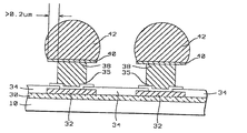
図5において断面で示されているのは、本発明のはんだバンプの第1のプロフィールであり、このはんだバンプのエレメントは以下の通りである:
−10、その上にはんだバンプが作製される半導体表面であって、一般にはシリコン半導体基板の表面である;
−30、半導体表面10を覆うように付着させた誘電体層;
−32、誘電体層30の表面上に作製された導体パッド;
−34、誘電体層30の表面を覆うように付着させた、パターン焼き付けされたパシベーション層; パシベーション層34に開口が造られていて、導体パッド32の表面を部分的に露出させている;
−36、等方的にエッチングされたバリヤー金属層; このバリヤー金属層は等方的にエッチングされているので、バリヤー金属は、パシベーション層34の表面から完全に除去されている(但し、オーバーレイしているはんだバンプのピラー金属(38)によってバリヤー金属が被覆されている場合は除く);
−38、はんだバンプのピラー金属;
−40、はんだバンプのピラー金属38をオーバーレイするように作製されたアンダーバンプ金属の層;
−40、はんだ金属。
Shown in cross-section in FIG. 5 is a first profile of a solder bump of the present invention, the elements of which are as follows:
-10, a semiconductor surface on which solder bumps are made, generally the surface of a silicon semiconductor substrate;
-30, a dielectric layer deposited over the
-32, a conductor pad made on the surface of the
-34, pattern-baked passivation layer deposited over the surface of
-36, isotropically etched barrier metal layer; since this barrier metal layer is isotropically etched, the barrier metal is completely removed from the surface of the passivation layer 34 (however, overlaid) Except when the barrier metal is covered by the pillar metal (38) of the solder bumps)
-38, pillar metal of solder bumps;
-40, a layer of underbump metal made to overlay the solder
-40, solder metal.
図6にて断面で示されているのは、本発明のはんだバンプの第2のプロフィールであり、このはんだバンプのエレメントは、異方的にエッチングされた層35(バリヤー金属層)が、異方性エッチングの特質により、図6の断面にて示すようにピラー金属38に対して突き出ている、という点を除けば、本発明のはんだバンプの第1のプロフィールに関して記載したエレメントと同じである。
Shown in cross-section in FIG. 6 is a second profile of the solder bump of the present invention, in which the element of the solder bump has an anisotropically etched layer 35 (barrier metal layer) that is different. Is the same as the element described with respect to the first profile of the solder bump of the present invention, except that due to the nature of the isotropic etching, it protrudes against the
図7〜16は、図5と6にて断面で示されているはんだバンプが得られる、本発明のプロセスの詳細を示している。
図7は、基板10の表面上部分の断面を示している。以下にエレメントについて記載する:
−10、シリコン基板であり、その表面上に金属導体パッド32が作製されている;
−30、基板10の表面を覆うように付着させた誘電体層;
−32、金属導体パッド、一般にはアルミニウムを含み、誘電体層30の表面上に作製される;
−34、誘電体層30の表面を覆うように付着させたパシベーション層であり、金属導体パッド32と整列していて、導体パッド32の表面を部分的に露出させている開口がパシベーション層34に作製されている;
−36、パシベーション層34の表面を覆うように作製されたバリヤー金属層であって、パシベーション層34に作製されている開口を含み、下側に存在する導体パッド32と接触している。
FIGS. 7-16 show details of the process of the present invention in which the solder bumps shown in cross section in FIGS. 5 and 6 are obtained.
FIG. 7 shows a cross section of the upper portion of the surface of the
-10, a silicon substrate with
-30, a dielectric layer deposited over the surface of the
-32, comprising metal conductor pads, generally aluminum, made on the surface of the
-34, a passivation layer deposited so as to cover the surface of the
-36, a barrier metal layer produced so as to cover the surface of the
層30に対する誘電体材料としては、一般的に使用されている誘電体材料〔たとえば、二酸化ケイ素(ドーピングされている場合と、そうでない場合)、オキシ窒化ケイ素、パリレン、ポリイミド、スピン−オン−ガラス(spin−on−glass)、プラズマ酸化物、またはLPCVD酸化物など〕のいずれも使用することができる。本発明の誘電体層30の付着に対して使用される材料は上記材料に限定されず、当業界において広く使用されている誘電体のいずれも使用できる。
The dielectric material for
金属導体パッド32の作製に対しては、たとえばアルミニウム−銅材料(アルミニウム導体パッド作製用)を供給源として使用し、約100〜400℃の温度および約1〜100ミリトルの圧力にて約10〜400sccmの流量で約400〜11000オングストロームの厚さに金属rfスパッタリングするという従来法を使用することができる。金属層を付着させた後、パターン焼き付けとエッチングを行ってアルミニウム導体パッド32を作製しなければならない。このパターン焼き付けとエッチングでは、従来の写真平板法、従来のパターン焼き付け法、および従来のエッチング法が使用される。Al−Cuの付着層は、Cl2/Arをエッチング液として使用して、50〜200℃の温度にて、Cl2に対しては約20sccmの、Arに対しては1000sccmのエッチング液流量にて、約50ミリトル〜約10トルの圧力にて、30〜200秒のエッチング時間でエッチングすることができる。
For the production of the
代表的なアプリケーションでは、半導体素子もしくは半導体基板における導線(conducting lines)の種々の層の表面上に化学蒸着(CVD)法を使用して絶縁層(たとえば、酸化ケイ素や酸素含有ポリマー)を付着させて、導電性の相互接続線を互いに隔離する。相互接続線のパターン焼き付け層上にさらに絶縁層を付着させることができ、絶縁層に金属バイアスが造られた状態で相互接続線の連続層間の電気的接触が確立される。チップに対する電気的接触は一般に、相互接続金属線のパターン焼き付けレベルとの電気的インターフェースを形成するボンディング・パッドまたは導体パッドによって確立される。信号線と電源/接地線は、ボンディング・パッドまたは導体パッドに接続することができる。ボンディング・パッドまたは導体パッドをチップの表面上に作製した後、ボンディング・パッドの表面を覆うようにパシベーション層を付着させることによってボンディング・パッドまたは導体パッドを不動態化し、電気的に絶縁する。パシベーション層は、CVDによって付着される酸化ケイ素/窒化ケイ素(SiO2/Si3N4)を含有してよい。このパシベーション層をパターン焼き付け及びエッチングして、パシベーション層にボンディング・パッドまたは導体パッドのための開口を作製し、その後に第2の比較的厚いパシベーション層を付着させて、さらなる絶縁、ならびに湿気や汚染物からの、またチップ集成時における機械的損傷からのチップ表面のさらなる保護を果たすことができる。 In a typical application, an insulating layer (eg, silicon oxide or an oxygen-containing polymer) is deposited using chemical vapor deposition (CVD) methods on the surface of various layers of conducting lines in a semiconductor device or semiconductor substrate. The conductive interconnect lines are isolated from each other. An additional insulating layer may be deposited on the interconnect line pattern burn-in layer, and electrical contact between successive layers of the interconnect line is established with a metal bias created in the insulating layer. Electrical contact to the chip is typically established by bonding pads or conductor pads that form an electrical interface with the pattern burn-in level of the interconnect metal lines. Signal lines and power / ground lines can be connected to bonding pads or conductor pads. After the bonding pad or conductor pad is fabricated on the surface of the chip, the bonding pad or conductor pad is passivated and electrically insulated by applying a passivation layer to cover the surface of the bonding pad. The passivation layer may contain silicon oxide / silicon nitride (SiO 2 / Si 3 N 4 ) deposited by CVD. This passivation layer is pattern baked and etched to create openings for bonding or conductor pads in the passivation layer, followed by deposition of a second relatively thick passivation layer for further insulation as well as moisture and contamination. Further protection of the chip surface from objects and from mechanical damage during chip assembly can be achieved.
パシベーション層の作製に対しては種々の材料が使用されている。パシベーション層は、CVDによって付着させた酸化ケイ素/窒化ケイ素(SiO2/Si3N4)を含有してよく、感光性ポリイミドの層であってもよく、あるいは窒化チタンを含んでもよい。パシベーション層に対して使用されることの多い他の材料はリンをドーピングした二酸化ケイ素であり、一般には、低温CVD法を使用して、アルミニウム相互接続物の最終層上に付着させる。近年、パシベーション層の作製に対しては、感光性ポリイミドが使用されることが多い。従来のポリイミドは、半導体素子構造物におけるアプリケーションに対して多くの優れた特性を有する。感光性ポリイミドはこれらの同じ特性を有するが、これに加えて、フォトレジストマスクのようにパターン焼き付けすることができ、またパターン焼き付けとエッチングの後に、表面上に残存してパシベーション層として機能することもできる。一般には、表面の接着性を向上させ、緊張状態を低下させるために、たとえば従来のフォトレジスト・スピン・コーティングによって、先ず最初に前駆体層を付着させる。低温でのプリベーク(pre−bake)の後に、たとえばステップアンドリピート式投影露光装置と光源としての紫外線とを使用して、この前駆体を露出させる。このようにして露出させた前駆体の部分に対して架橋反応を起こさせ、これによって、露出していない区域(架橋していない区域)がボンディング・パッド上に残る。引き続き行われる現像操作時において、露出していないポリイミド前駆体層(ボンディング・パッド上)が溶解され、これによってボンディング・パッド上に開口が得られる。熱キュアーの最終工程を施すことにより、ポリイミドの耐久性高品質パシベーション層が残る。 Various materials are used for the fabrication of the passivation layer. The passivation layer may contain silicon oxide / silicon nitride (SiO 2 / Si 3 N 4 ) deposited by CVD, may be a layer of photosensitive polyimide, or may contain titanium nitride. Another material often used for the passivation layer is phosphorus-doped silicon dioxide, which is typically deposited on the final layer of aluminum interconnect using a low temperature CVD process. In recent years, photosensitive polyimide is often used for the production of a passivation layer. Conventional polyimides have many excellent properties for applications in semiconductor device structures. Photosensitive polyimide has these same properties, but in addition, it can be pattern-baked like a photoresist mask, and remains on the surface after pattern baking and etching to function as a passivation layer. You can also. In general, the precursor layer is first deposited, for example by conventional photoresist spin coating, to improve surface adhesion and reduce tension. After pre-bake at low temperature, the precursor is exposed using, for example, a step-and-repeat projection exposure apparatus and ultraviolet light as a light source. The exposed portion of the precursor is allowed to undergo a crosslinking reaction, thereby leaving unexposed areas (non-crosslinked areas) on the bonding pad. During subsequent development operations, the unexposed polyimide precursor layer (on the bonding pad) is dissolved, thereby providing an opening on the bonding pad. By applying the final step of thermal cure, a durable high quality passivation layer of polyimide remains.
パシベーション層34を付着させるための本発明の好ましい材料はプラズマ・エンハンスト窒化ケイ素(PE Si3N4)であり、PECVD技術を使用して、約350〜450℃の温度および約2.0〜2.8トルの圧力にて、約8〜12秒の継続時間で付着させる。PE Si3N4の層32は、約200〜800オングストロームの厚さに付着させることができる。
A preferred material of the present invention for depositing the
次いで、PE Si3N4の層34をパターン焼き付け及びエッチングして、下側に存在する導体パッド32にオーバーレイしていて且つ整列している開口を層34中に作製する。
The PE Si 3 N 4 layer 34 is then pattern baked and etched to create an opening in the
パシベーション層34のエッチングは、乾式エッチングプロセスに従って、Ar/CF4をエッチング液として使用し、約120〜160℃の温度および約0.30〜0.40トルの圧力にて約33〜39秒行うことができる。
The
パシベーション層34のエッチングはさらに、乾式エッチングプロセスに従って、He/NF3をエッチング液として使用し、約80〜100℃の温度および約1.20〜1.30トルの圧力にて約20〜30秒行うことができる。
Etching of the
バリヤー層(たとえば層36)は通常、周囲の誘電体層およびシリコン層への相互接続金属の拡散を防ぐために使用される。相互接続金属のための銅を1つの例として使用することによって、バリヤー層のための材料を選択する上で適用される考え方の幾つかが明らかになる。銅は比較的コストが低く、抵抗率が低いけれども、二酸化ケイ素やケイ素中への拡散係数が比較的大きく、従って一般には相互接続金属としては使用されない。銅は、相互接続物から二酸化ケイ素の層中に拡散することがあり、従って誘電体が導電性になり、二酸化ケイ素層の絶縁耐力が低下する。銅の相互接続物は、少なくとも1つの拡散バリヤーによって封入して、二酸化ケイ素層への拡散を防止しなければならない。窒化ケイ素は銅に対する拡散バリヤーであるが、従来技術によれば、相互接続物は二酸化ケイ素と比較して高い誘電率を有するので、相互接続物が窒化ケイ素層の上に存在すべきではないとされている。誘電率が高いと、相互接続物と基板との間にキャパシタンスの所望の増大を引き起こす。 A barrier layer (eg, layer 36) is typically used to prevent diffusion of interconnect metal into the surrounding dielectric and silicon layers. Using copper for the interconnect metal as an example reveals some of the concepts applied in selecting the material for the barrier layer. Although copper is relatively inexpensive and has a low resistivity, it has a relatively high diffusion coefficient into silicon dioxide and silicon and is therefore generally not used as an interconnect metal. Copper may diffuse from the interconnect into the silicon dioxide layer, thus making the dielectric conductive and reducing the dielectric strength of the silicon dioxide layer. The copper interconnect must be encapsulated by at least one diffusion barrier to prevent diffusion into the silicon dioxide layer. Although silicon nitride is a diffusion barrier to copper, according to the prior art, the interconnect should have a higher dielectric constant compared to silicon dioxide, so that the interconnect should not be on the silicon nitride layer. Has been. A high dielectric constant causes the desired increase in capacitance between the interconnect and the substrate.
典型的な拡散バリヤー層は、窒化ケイ素、ホスホシリケートガラス(PSG)、オキシ窒化ケイ素、アルミニウム、酸化アルミニウム(AlxOy)、タンタル、Ti/TiN、Ti/W、ニオブ、またはモリブデンを含有してよく、TiNから形成されるのがさらに好ましい。バリヤー層はさらに、オーバーレイしているタングステン層の密着性を向上させるのにも使用することができる。 Typical diffusion barrier layers contain silicon nitride, phosphosilicate glass (PSG), silicon oxynitride, aluminum, aluminum oxide (Al x O y ), tantalum, Ti / TiN, Ti / W, niobium, or molybdenum. More preferably, it is made of TiN. The barrier layer can also be used to improve the adhesion of the overlying tungsten layer.
バリヤー層の厚さは約500〜2000オングストロームであるのが好ましく、約300オングストロームであるのがさらに好ましく、rfスパッタリングを使用して付着させることができる。 The thickness of the barrier layer is preferably about 500-2000 angstroms, more preferably about 300 angstroms, and can be deposited using rf sputtering.
バリヤー層36を作製した後、ウエハーの表面を覆うようにしてシード層(図7には示されていない)をブランケット付着させることができる。ウエハーの表面上に付着させるシード層に対しては、従来の金属シード材料のいずれも使用することができる。金属シード層は、スパッター・チャンバーまたはイオンメタルプラズマ(IMP)チャンバーを約0〜300℃の温度および約1〜100ミリトルの圧力にて使用し、たとえば銅または銅合金を供給源として約10〜400sccmの流量にて使用して(前述)、そしてアルゴンを周囲ガスとして使用して付着させることができる。
After creating the
図8は、バリヤー層36の表面上にフォトレジスト層37を付着させた後の基板の断面を示している。フォトレジスト層37をパターン焼き付け及びエッチングし、フォトレジスト層37に開口31を作製する。開口31は、バリヤー層36の表面を部分的に露出させる。フォトレジスト層37は、通常は約100〜200μmの厚さに、さらに好ましくは約150μmの厚さに施す。
FIG. 8 shows a cross section of the substrate after a
フォトレジスト層37は、通常は約100〜200μmの厚さに、さらに好ましくは約150μmの厚さに施す。フォトレジスト層37の付着と現像に対して使用される方法は従来の写真平板法を使用する。写真平板は広く使用されている方法であり、該方法によれば、フォトレジスト層に対してスピニングし、フォトレジストをパターンに従って露出させるよう所望のパターンを有するフォトマスクを通してフォトレジスト上に光を投射し、フォトレジストを現像し、現像されていないフォトレジストを洗い落とし、そしてプラズマエッチングして、フォトレジストが洗い落とされた区域を清浄にすることによって、パターン焼き付けされた層が形成される。露出されたレジストを可溶性にして(ポジティブ・ワーキング)洗い落とすこともできるし、あるいは不溶性にして(ネガティブ・ワーキング)パターンを形成させることもできる。
The
付着させたフォトレジスト層37に対し、パターン焼き付けとエッチングの前にキュアーまたはプリベークして、フォトレジスト層37の表面をさらに硬化させることができる。
The surface of the
フォトレジスト層37は、O2プラズマを施し、次いでH2SO4溶液、H2O2溶液、およびNH4OH溶液を使用して湿潤ストリッピングすることによってエッチングすることができる。フォトレジストを他の手段によってストリッピングした後には、硫酸(H2SO4)およびH2SO4と他の酸化剤〔たとえば過酸化水素(H2O2)〕との混合物が広く使用されている。ストリッピングしようとするウエハーを混合物中に約100℃〜約150℃の温度で5〜10分浸漬し、脱イオン水を使用して清浄化処理し、そして乾燥窒素によって乾燥することができる。強くポストベークされたレジストを残留物が残らないよう除去するには、無機レジストストリッパー(たとえば硫酸混合物)が極めて有効である。これらは有機ストリッパーより有効であり、浸漬時間を長くするほど、より清浄で且つより残留物の少ない表面を得ることができる。
フォトレジスト層37はさらに、プラズマ酸素アッシングと慎重なウェット・クリーニングを使用して部分的に除去することもできる。酸素プラズマアッシングは、フォトレジストを高度に酸化された環境(たとえば酸素プラズマ)において加熱することであり、これによりフォトレジストが容易に除去されるアッシュに転化される。酸素プラズマアッシングの後に、フッ化水素酸の200:1希釈溶液中にて90秒ネイティブ・オキシド・ディップ(a native oxide dip)を行うことができる。
The
図9は、フォトレジスト層37中に作製されている開口31によって拘束されるピラー金属層38をバリヤー材料層36の表面上に付着(電気メッキにより)させた後の、基板10の断面を示している。金属層38(これらの層が本発明のはんだバンプの完成構造物において果たす役割から見て、この金属はピラー金属と呼ばれる)の表面上に、アンダーバンプ金属の層40が電気メッキ等の付着法を使用して付着されている。
FIG. 9 shows a cross section of the
層36はチタンまたは銅を含むのが好ましく、約500〜2000オングストロームの厚さに付着させるのが好ましく、約1000オングストロームの厚さに付着させるのがさらに好ましい。
層38は銅を含むのが好ましく、約10〜100μmの厚さに施すのが好ましく、約50μmの厚さに施すのがさらに好ましい。
層40はニッケルを含むのが好ましく、約1〜10μmの厚さに施すのが好ましく、約4μmの厚さに施すのがさらに好ましい。
図10は、本発明のプロセスが、フォトレジスト層37中に作製されている開口31によって拘束されるはんだ金属の電気メッキ層42を、アンダーバンプ金属(UBM)層40の表面上にさらに有している場合の断面を示している。
FIG. 10 shows that the process of the present invention further has a solder metal electroplated
UBM層40(一般にはニッケルであって、厚さは約1〜10μm)は、ピラー金属層38を覆うように電気メッキする。バンプ金属(一般にははんだ)の層42は、UBM層40と接触している状態にて約30〜100μmの厚さに、さらに好ましくは約50μmの厚さに電気メッキして作製する。電気メッキした金属の層38、40、および42は、フォトレジスト層37中に作製されている開口31に中心を置いている。
The UBM layer 40 (generally nickel and about 1-10 μm thick) is electroplated over the
図11に示されている断面においては、パターン焼き付けされたフォトレジスト層37がバリヤー層36の表面上から除去された状態が示されている。フォトレジスト層を除去するための前述の方法とプロセシング条件を、図11の断面にて示されているような層37の除去のためにも適用することができる。本発明ではさらに、図12の断面にて示すように、ピラー金属材料に対して選択的な湿式化学エッチング法または等方性乾式エッチング法を使用してピラー金属38の部分エッチングを行う。言うまでもないことであるが、エッチングパラメーター(このうちエッチング時間が最も有益である)を調節することによって、ピラー金属層38の直径を所望する殆どいかなる値にも減少させることができる。ピラー金属層38の直径が減少される程度に対して及ぼされる制約は、湿式エッチングプロセスによって及ぼされることはないが、金属バンプの信頼性および機能性に対しては問題が生じる。ピラー金属層38の残留直径があまりにも小さいと、はんだバンプの堅牢性に影響を及ぼし、また金属バンプの抵抗を増大させるという影響を及ぼすことがある。
The cross section shown in FIG. 11 shows a state in which the pattern-
はんだ金属がリフローされる前の本発明の最終的な2つのプロセシング工程が図13と図14の断面に示されており、バリヤー層36の露出表面のエッチングに影響を及ぼす。等方性エッチングを使用して(図13)、露出されたバリヤー層が完全に除去される。異方性エッチングを使用して(図14)、はんだ金属のカラム42の存在よって、バリヤー層のエッチングが部分的に妨げられる。
The final two processing steps of the present invention before the solder metal is reflowed are shown in the cross sections of FIGS. 13 and 14 and affect the etching of the exposed surface of the
ピラー38のアンダーカット形状により、引き続き行われるはんだリフロー時におけるピラー38とUBM層40のウェッティングが防止される、と考えられる。さらに、空気に露出されることによって、ピラー38とUBM層40のサイドウォールが酸化され、従って引き続き行われるはんだリフロー時におけるこれら表面のウェッティングが防止される、と考えられる。必要に応じて、ピラー38とUBM層40のサイドウォールは、たとえば約240℃のリフロー温度未満での熱酸化(たとえば約125℃における酸素雰囲気での加熱)によってさらに酸化してもよい。
It is considered that the undercut shape of the
図15と図16は、はんだ金属がリフローされた後の、本発明のはんだバンプの最終的な断面を示している。図15は図13に、そして図16は図14に対応しており、図13と図14を使用して説明されたバリヤー層36のエッチングに関係している。図15における断面で示されているエッチングされたバリヤー材料層36は、図13において示されているエッチングされたバリヤー材料層に対応している、という点に留意しなければならない。図16と図14との間に同じ対応が存在する。
15 and 16 show the final cross section of the solder bump of the present invention after the solder metal has been reflowed. FIG. 15 corresponds to FIG. 13 and FIG. 16 corresponds to FIG. 14 and relates to the etching of the
金属バンプの作製に対して使用される上記のプロセシング工程(電気メッキ工程)は、フォトレジスト層の付着後にこのフォトレジスト層をキュアーまたはプリベークする工程で補足することができる。 The processing step (electroplating step) used for the production of metal bumps can be supplemented with a step of curing or pre-baking the photoresist layer after deposition of the photoresist layer.
本発明を要約すると以下のようになる:
・本発明の準備にあたって、半導体表面を供給し、半導体表面上に誘電体層を付着させ、誘電体層上に導体パッドを供給し、導体パッドが露出表面を有し、前記導体パッドの表面を含めた半導体表面上にパシベーション層を付着させ、パシベーション層に対しパターン焼き付けとエッチングを施し、これによりパシベーション層中に開口を作製し、導体パッドの表面を部分的に露出させ、パシベーション層中の開口を導体パッドに関して中心に配置する。
The summary of the present invention is as follows:
In preparation of the present invention, a semiconductor surface is supplied, a dielectric layer is deposited on the semiconductor surface, a conductor pad is supplied on the dielectric layer, the conductor pad has an exposed surface, and the surface of the conductor pad is A passivation layer is deposited on the included semiconductor surface, pattern baking and etching are performed on the passivation layer, thereby creating an opening in the passivation layer, partially exposing the surface of the conductor pad, and opening in the passivation layer. Is centered with respect to the conductor pads.
・本発明は、パシベーション層の表面上に付着させたバリヤー層からスタートしており、パシベーション層中に作製されている開口を通して導体パッドと接触している。
・バリヤー層の表面上にフォトレジスト層を付着させる。
The invention starts with a barrier layer deposited on the surface of the passivation layer and is in contact with the conductor pad through an opening made in the passivation layer.
Deposit a photoresist layer on the surface of the barrier layer.
・フォトレジスト層に対しパターン焼き付けとエッチングを施してフォトレジスト層を貫く開口を作製し、このフォトレジスト中の開口を、導体パッドに関して整列させて中心に置くようにする。 Pattern baking and etching the photoresist layer to create an opening through the photoresist layer, with the opening in the photoresist aligned and centered with respect to the conductor pad.
・ピラー金属層、アンダーバンプ金属層、およびはんだ金属層をこの順序にて、フォトレジスト層中に作製されている開口によって拘束される状態で付着させる。
・パターン焼き付けされたフォトレジスト層をバリヤー層の表面から除去する。
The pillar metal layer, the under bump metal layer, and the solder metal layer are attached in this order in a state constrained by the opening formed in the photoresist layer.
Remove the pattern-baked photoresist layer from the surface of the barrier layer.
・ピラー金属層をエッチングし、ピラー金属の直径を減少させる。
・等方性エッチングまたは異方性エッチングを使用してバリヤー層をエッチングする。
・はんだ金属をリフローする。
Etch the pillar metal layer to reduce the pillar metal diameter.
Etch the barrier layer using isotropic or anisotropic etching.
・ Reflow solder metal.
本発明は以下のような利点をもたらす。
・信頼性を高める上でボールの高さが極めて重要なポイントである。パッケージのオーバーレイ層間の熱的不整合を防止するために(たとえば、半導体素子と下側に存在するプリント回路基板など)、オーバーレイしているエレメント間の距離を増大させることが重要である。本発明では、こうしたことが達成される。
The present invention provides the following advantages.
-The height of the ball is an extremely important point for improving reliability. In order to prevent thermal mismatch between the overlay layers of the package (e.g., a semiconductor element and an underlying printed circuit board), it is important to increase the distance between the overlaid elements. In the present invention, this is achieved.
・はんだボールがより大きくなると(より良好な熱的性能又はより高い信頼性を得るために)ピッチが増大し、この点は、最新技術に基づく設計要件とは相容れない。
・高さを与えることなく小さなはんだボールが使用される場合、小さな隙間をアンダーフィルするのが極めて困難である。
-The larger the solder balls, the greater the pitch (to obtain better thermal performance or higher reliability), which is incompatible with design requirements based on the latest technology.
-When small solder balls are used without giving height, it is extremely difficult to underfill small gaps.
・本発明を使用すると、はんだが半導体素子から比較的離れた個所にて除去され、このことは低−αはんだを施す必要がないということを意味している(α−粒子はメモリー物品においてソフト上のエラーを生じ、鉛は、腐食するとα−粒子を放出することが知られている)。 Using the present invention, the solder is removed at a location that is relatively far from the semiconductor element, which means that it is not necessary to apply low-alpha solder (alpha particles are soft in memory articles) It causes the above error, and lead is known to release α-particles when it corrodes).
・ピラー金属に関しては、良好な導電性と延性を有する金属(たとえば銅)を選択する必要がある。これは、熱応力の影響を弱めることによって改良された熱的性能を得るためのものである。 -As for the pillar metal, it is necessary to select a metal (for example, copper) having good conductivity and ductility. This is to obtain improved thermal performance by reducing the effects of thermal stress.
・本発明のはんだバンプのピラーの高さが重要であり、高いスタンドオフという目的を達成するために約10〜100μmでなければならない。
・アンダーバンプ金属層のために使用される金属は、はんだリフロー時にオーバーレイしているはんだに対して良好な接着性を有していなければならないが、あまりにも早く溶解してはならず、また早く溶解した場合にははんだに対するバリヤーを形成しなければならない、という点において重要である。さらに、UBM金属は、空気にさらされると保護酸化物層を形成することがあり、従ってリフロープロセス時において、UBM金属の周りでのピラー金属に対するはんだウェッティングが妨げられる。従ってUBM金属にはニッケルが好ましい。
The pillar height of the solder bumps of the present invention is important and should be about 10-100 μm to achieve the goal of high standoff.
The metal used for the underbump metal layer must have good adhesion to the overlaying solder during solder reflow, but it must not dissolve too quickly and quickly This is important in that, when melted, a barrier to the solder must be formed. In addition, UBM metal can form a protective oxide layer when exposed to air, thus preventing solder wetting of the pillar metal around the UBM metal during the reflow process. Therefore, nickel is preferred for the UBM metal.
幾つかの特定の実施態様に関して本発明を説明してきたが、本発明がこれらの実施態様に限定されることはない。本発明の精神を逸脱することなく種々の変形や改良形が可能であることは、当業者にとっては言うまでもないことである。従って、特許請求の範囲の範囲内に含まれるこのような全ての変形や改良形も本発明に含まれるものとする。 Although the invention has been described with reference to several specific embodiments, the invention is not limited to these embodiments. It goes without saying to those skilled in the art that various modifications and improvements can be made without departing from the spirit of the invention. Accordingly, all such modifications and improvements that fall within the scope of the claims are intended to be included in the present invention.
Claims (46)
半導体表面を供給する工程;
導体パッドに対する開口を設けたパシベーション層をその上に有する、前記半導体表面を覆う導体パッドを供給する工程、このときパシベーション層の表面を覆うように、および前記開口中にバリヤー層が付着されている;
フォトレジスト層を、前記バリヤー層を覆うように付着させる工程;
前記フォトレジスト中に、導体パッドと整列したピラー開口を形成する工程;
前記ピラー開口中にピラー金属の層を付着させる工程;
アンダーバンプ金属の層を、前記ピラー金属を覆うように付着させる工程;
はんだ金属の層を、前記アンダーバンプ金属を覆うように付着させる工程;
フォトレジスト層を除去する工程;
ピラー金属層の直径を減少させる工程;
バリヤー層をエッチングする工程; および
はんだ金属をリフローして前記金属バンプを形成する工程;
を含む前記方法。 A method for forming metal bumps on a semiconductor surface,
Supplying a semiconductor surface;
A step of supplying a conductor pad covering the semiconductor surface, having a passivation layer provided with an opening for the conductor pad thereon, a barrier layer being attached to cover the surface of the passivation layer at this time ;
Depositing a photoresist layer over the barrier layer;
Forming a pillar opening in the photoresist aligned with the conductor pad;
Depositing a layer of pillar metal in the pillar opening;
Depositing a layer of underbump metal over the pillar metal;
Depositing a layer of solder metal over the underbump metal;
Removing the photoresist layer;
Reducing the diameter of the pillar metal layer;
Etching the barrier layer; and reflowing solder metal to form the metal bumps;
Including said method.
前記半導体表面を覆う誘電体層;
第1の材料で造られた、前記誘電体層を覆う導体パッド;
前記導体パッドと整列した開口を有する、前記誘電体層を覆うパシベーション層;
前記パシベーション層中に造られた前記開口を含む、前記誘電体層を覆うように付着させたバリヤー層; および
導体パッドと整列していて、導体パッドの表面エリアにほぼ等しい直径を有していて、バリヤー層と接触しているある層からはじまっている、ピラー金属層、アンダーバンプ金属層、およびはんだ金属層の3つの金属層で構成されるスタック;
を含み、このとき
前記ピラー金属の直径が適度の量だけ減少されており;
前記バリヤー層が、等方性エッチング法または異方性エッチング法を使用して除去されており; そして
前記はんだ金属がリフローされている;
金属バンプ接点。 Semiconductor surface;
A dielectric layer covering the semiconductor surface;
A conductor pad made of a first material and covering the dielectric layer;
A passivation layer covering the dielectric layer having openings aligned with the conductor pads;
A barrier layer deposited over the dielectric layer, including the opening made in the passivation layer; and aligned with the conductor pad and having a diameter approximately equal to the surface area of the conductor pad. A stack composed of three metal layers starting from one layer in contact with the barrier layer, a pillar metal layer, an under bump metal layer, and a solder metal layer;
Wherein the diameter of the pillar metal is reduced by a reasonable amount;
The barrier layer is removed using an isotropic or anisotropic etching method; and the solder metal is reflowed;
Metal bump contact.
前記パシベーション層中に造られた開口を含んだバリヤー材料層を、前記パシベーション層の表面を覆うように付着させる工程;
金属の付着を妨げる材料の層を、バリヤー層の表面を覆うように付着させる工程;
金属の付着を妨げる材料の層をパターン焼き付け及びエッチングし、金属の付着を妨げる材料層中に、導体パッドと整列していて、導体パッドの表面エリアにほぼ等しい直径を有する開口を造る工程;
導体パッドと整列している表面エリア上のバリヤー層表面を部分的に露出させる工程;
ピラー金属の層を、バリヤー層の露出表面を覆うように付着させる工程;
アンダーバンプメタラージ(UBM)の層を、ピラー金属層の表面を覆うように付着させる工程;
バンプ金属の層を、UBM層の表面を覆うように付着させる工程;
金属の付着を妨げる材料の層をバリヤー層の表面上から取り除く工程;
ピラー金属の層をエッチングし、ピラー材料の直径を適度の量だけ減少させる工程;
等方性エッチング法または異方性エッチング法を使用して、前記パシベーション層の表面から前記バリヤー層を除去する工程; および
前記はんだ金属をリフローして金属バンプを形成する工程;
を含む、半導体表面上に金属バンプを形成する方法。 Supplying a semiconductor surface over which the semiconductor surface is provided and having a passivation layer provided thereon with an opening for the conductor pad;
Depositing a barrier material layer including openings made in the passivation layer so as to cover the surface of the passivation layer;
Depositing a layer of material that prevents metal deposition over the surface of the barrier layer;
Pattern baking and etching a layer of material that prevents metal deposition to create an opening in the material layer that prevents metal deposition that is aligned with the conductor pad and has a diameter approximately equal to the surface area of the conductor pad;
Partially exposing the barrier layer surface over the surface area aligned with the conductor pads;
Depositing a layer of pillar metal over the exposed surface of the barrier layer;
Depositing an under bump metallurgy (UBM) layer over the surface of the pillar metal layer;
Depositing a bump metal layer over the surface of the UBM layer;
Removing from the surface of the barrier layer a layer of material that prevents metal adhesion;
Etching the pillar metal layer and reducing the diameter of the pillar material by a reasonable amount;
Removing the barrier layer from the surface of the passivation layer using an isotropic or anisotropic etching method; and reflowing the solder metal to form metal bumps;
Forming a metal bump on a semiconductor surface.
表面もしくは表面上に導体パッドが設けられている半導体表面を供給する工程、このとき前記導体パッドは、下側に存在する誘電体層上に位置しており、前記支持体の表面もしくは表面上における電気接点の少なくとも1個所と電気的に接触している;
表面層としてのバリヤー層を有する、前記金属パンプのためのベース層を供給する工程;
ピラー金属層、アンダーバンプ金属層、およびはんだ金属層の3つの連続した層を含む、前記金属パンプのためのカラムを供給する工程; および
前記金属バンプを供給する工程;
を含む前記方法。 A method for forming metal bumps on a semiconductor surface,
Supplying a semiconductor surface provided with a conductor pad on the surface or on the surface, wherein the conductor pad is located on a dielectric layer present on the lower side, on the surface of the support or on the surface; In electrical contact with at least one of the electrical contacts;
Providing a base layer for the metal pump having a barrier layer as a surface layer;
Providing a column for the metal bump comprising three successive layers of a pillar metal layer, an under bump metal layer, and a solder metal layer; and supplying the metal bump;
Including said method.
前記導体パッドの表面を含めて、導体パッドの下側に存在する前記誘電体層の表面を覆うようにパシベーション層を付着させる工程;
前記パシベーション層をパターン焼き付け及びエッチングし、前記パシベーション層に開口を作製し、そして前記導体パッドの表面を部分的に露出させる工程、このとき前記パシベーション層において作製された前記開口は、前記導体パッドの表面エリアより適度の量だけ小さい; および
前記パシベーション層において作製された開口を含めて、前記パシベーション層の表面を覆うようにバリヤー材料の層を付着させる工程;
を含む、請求項21記載の方法。 Providing the base layer for the metal bumps comprises:
Applying a passivation layer so as to cover the surface of the dielectric layer existing below the conductor pad, including the surface of the conductor pad;
Pattern-baking and etching the passivation layer, creating an opening in the passivation layer, and partially exposing a surface of the conductor pad, wherein the opening made in the passivation layer is formed on the conductor pad; Depositing a layer of barrier material to cover the surface of the passivation layer, including openings made in the passivation layer;
The method of claim 21, comprising:
金属の付着を妨げる材料の層を、バリヤー層の表面を覆うように付着させる工程;
金属の付着を妨げる材料の層をパターン焼き付け及びエッチングし、導体パッドと整列していて、導体パッドの表面にほぼ等しい直径を有する開口を、金属の付着を妨げる材料の層において作製し、そして導体パッドと整列している表面エリア上のバリヤー層の表面を部分的に露出させる工程;
ピラー金属の層を、バリヤー層の露出表面を覆うように付着させる工程;
アンダーバンプメタラージ(UBM)の層を、ピラー金属層の表面を覆うように付着させる工程;
バンプ金属の層を、UBM層の表面を覆うように付着させる工程;
金属の付着を妨げる材料の層をバリヤー層の表面上から取り除く工程;
ピラー金属層をエッチングし、ピラー金属の直径を適度の量だけ減少させる工程;および
等方性エッチング法または異方性エッチング法を使用して、前記パシベーション層の表面から前記バリヤー層を取り除く工程;
を含む、請求項21記載の方法。 Supplying the column for the metal bumps comprises:
Depositing a layer of material that prevents metal deposition over the surface of the barrier layer;
Pattern-baking and etching a layer of material that prevents metal deposition, creating an opening in the layer of material that prevents metal deposition and aligned with the conductor pad and having a diameter approximately equal to the surface of the conductor pad Partially exposing the surface of the barrier layer on the surface area aligned with the pad;
Depositing a layer of pillar metal over the exposed surface of the barrier layer;
Depositing an under bump metallurgy (UBM) layer over the surface of the pillar metal layer;
Depositing a bump metal layer over the surface of the UBM layer;
Removing from the surface of the barrier layer a layer of material that prevents metal adhesion;
Etching the pillar metal layer to reduce the diameter of the pillar metal by an appropriate amount; and removing the barrier layer from the surface of the passivation layer using an isotropic or anisotropic etching method;
The method of claim 21, comprising:
Priority Applications (1)
| Application Number | Priority Date | Filing Date | Title |
|---|---|---|---|
| JP2006200592A JP2006332694A (en) | 2006-07-24 | 2006-07-24 | Method for forming metal bumps on semiconductor surface |
Applications Claiming Priority (1)
| Application Number | Priority Date | Filing Date | Title |
|---|---|---|---|
| JP2006200592A JP2006332694A (en) | 2006-07-24 | 2006-07-24 | Method for forming metal bumps on semiconductor surface |
Related Parent Applications (1)
| Application Number | Title | Priority Date | Filing Date |
|---|---|---|---|
| JP2002056997A Division JP2003258014A (en) | 2002-03-04 | 2002-03-04 | Method for forming metal bump on semiconductor surface |
Publications (2)
| Publication Number | Publication Date |
|---|---|
| JP2006332694A true JP2006332694A (en) | 2006-12-07 |
| JP2006332694A5 JP2006332694A5 (en) | 2008-11-27 |
Family
ID=37553969
Family Applications (1)
| Application Number | Title | Priority Date | Filing Date |
|---|---|---|---|
| JP2006200592A Pending JP2006332694A (en) | 2006-07-24 | 2006-07-24 | Method for forming metal bumps on semiconductor surface |
Country Status (1)
| Country | Link |
|---|---|
| JP (1) | JP2006332694A (en) |
Cited By (4)
| Publication number | Priority date | Publication date | Assignee | Title |
|---|---|---|---|---|
| JP2015018958A (en) * | 2013-07-11 | 2015-01-29 | インターナショナル・ビジネス・マシーンズ・コーポレーションInternational Business Machines Corporation | Mounting structure and method for manufacturing the same |
| JP2015216344A (en) * | 2014-04-21 | 2015-12-03 | 新光電気工業株式会社 | Wiring board and method of manufacturing the same |
| KR20160102150A (en) | 2013-12-27 | 2016-08-29 | 미쓰비시 마테리알 가부시키가이샤 | Solder bump having cored structure and production method therefor |
| JP2017183592A (en) * | 2016-03-31 | 2017-10-05 | 株式会社荏原製作所 | Method of manufacturing substrate and substrate |
Citations (5)
| Publication number | Priority date | Publication date | Assignee | Title |
|---|---|---|---|---|
| JPH05335313A (en) * | 1992-05-29 | 1993-12-17 | Toshiba Corp | Manufacture of indium bump |
| JPH0637093A (en) * | 1992-07-14 | 1994-02-10 | Sanken Electric Co Ltd | Forming method for bump electrode |
| JPH11163019A (en) * | 1997-12-01 | 1999-06-18 | Seiko Epson Corp | Semiconductor device and manufacture of the same |
| JP2001093928A (en) * | 1999-09-22 | 2001-04-06 | Toshiba Corp | Semiconductor device and its manufacturing method |
| JP2001257210A (en) * | 2000-03-10 | 2001-09-21 | Hitachi Ltd | Semiconductor integrated circuit device |
-
2006
- 2006-07-24 JP JP2006200592A patent/JP2006332694A/en active Pending
Patent Citations (5)
| Publication number | Priority date | Publication date | Assignee | Title |
|---|---|---|---|---|
| JPH05335313A (en) * | 1992-05-29 | 1993-12-17 | Toshiba Corp | Manufacture of indium bump |
| JPH0637093A (en) * | 1992-07-14 | 1994-02-10 | Sanken Electric Co Ltd | Forming method for bump electrode |
| JPH11163019A (en) * | 1997-12-01 | 1999-06-18 | Seiko Epson Corp | Semiconductor device and manufacture of the same |
| JP2001093928A (en) * | 1999-09-22 | 2001-04-06 | Toshiba Corp | Semiconductor device and its manufacturing method |
| JP2001257210A (en) * | 2000-03-10 | 2001-09-21 | Hitachi Ltd | Semiconductor integrated circuit device |
Cited By (4)
| Publication number | Priority date | Publication date | Assignee | Title |
|---|---|---|---|---|
| JP2015018958A (en) * | 2013-07-11 | 2015-01-29 | インターナショナル・ビジネス・マシーンズ・コーポレーションInternational Business Machines Corporation | Mounting structure and method for manufacturing the same |
| KR20160102150A (en) | 2013-12-27 | 2016-08-29 | 미쓰비시 마테리알 가부시키가이샤 | Solder bump having cored structure and production method therefor |
| JP2015216344A (en) * | 2014-04-21 | 2015-12-03 | 新光電気工業株式会社 | Wiring board and method of manufacturing the same |
| JP2017183592A (en) * | 2016-03-31 | 2017-10-05 | 株式会社荏原製作所 | Method of manufacturing substrate and substrate |
Similar Documents
| Publication | Publication Date | Title |
|---|---|---|
| US6818545B2 (en) | Low fabrication cost, fine pitch and high reliability solder bump | |
| US6426556B1 (en) | Reliable metal bumps on top of I/O pads with test probe marks | |
| US8158508B2 (en) | Structure and manufacturing method of a chip scale package | |
| US20080050909A1 (en) | Top layers of metal for high performance IC's | |
| US6586323B1 (en) | Method for dual-layer polyimide processing on bumping technology | |
| US6426281B1 (en) | Method to form bump in bumping technology | |
| US6605524B1 (en) | Bumping process to increase bump height and to create a more robust bump structure | |
| US6756294B1 (en) | Method for improving bump reliability for flip chip devices | |
| US6642136B1 (en) | Method of making a low fabrication cost, high performance, high reliability chip scale package | |
| US8481418B2 (en) | Low fabrication cost, high performance, high reliability chip scale package | |
| US7456090B2 (en) | Method to reduce UBM undercut | |
| JP2007502530A (en) | Semiconductor device with strain relief bump design | |
| US9269678B2 (en) | Bond pad structure and method of manufacturing the same | |
| US6479376B1 (en) | Process improvement for the creation of aluminum contact bumps | |
| JP2006332694A (en) | Method for forming metal bumps on semiconductor surface | |
| JP2003258014A (en) | Method for forming metal bump on semiconductor surface |
Legal Events
| Date | Code | Title | Description |
|---|---|---|---|
| A521 | Written amendment |
Free format text: JAPANESE INTERMEDIATE CODE: A523 Effective date: 20060823 |
|
| A621 | Written request for application examination |
Free format text: JAPANESE INTERMEDIATE CODE: A621 Effective date: 20060823 |
|
| A521 | Written amendment |
Free format text: JAPANESE INTERMEDIATE CODE: A523 Effective date: 20081008 |
|
| A977 | Report on retrieval |
Free format text: JAPANESE INTERMEDIATE CODE: A971007 Effective date: 20081201 |
|
| A131 | Notification of reasons for refusal |
Free format text: JAPANESE INTERMEDIATE CODE: A131 Effective date: 20081204 |
|
| A601 | Written request for extension of time |
Free format text: JAPANESE INTERMEDIATE CODE: A601 Effective date: 20090304 |
|
| A602 | Written permission of extension of time |
Free format text: JAPANESE INTERMEDIATE CODE: A602 Effective date: 20090309 |
|
| A521 | Written amendment |
Free format text: JAPANESE INTERMEDIATE CODE: A523 Effective date: 20090406 |
|
| A02 | Decision of refusal |
Free format text: JAPANESE INTERMEDIATE CODE: A02 Effective date: 20091030 |
|
| A521 | Written amendment |
Free format text: JAPANESE INTERMEDIATE CODE: A523 Effective date: 20100301 |
|
| A521 | Written amendment |
Free format text: JAPANESE INTERMEDIATE CODE: A523 Effective date: 20100804 |
|
| A911 | Transfer of reconsideration by examiner before appeal (zenchi) |
Free format text: JAPANESE INTERMEDIATE CODE: A911 Effective date: 20100826 |
|
| A912 | Removal of reconsideration by examiner before appeal (zenchi) |
Free format text: JAPANESE INTERMEDIATE CODE: A912 Effective date: 20101203 |
|
| A601 | Written request for extension of time |
Free format text: JAPANESE INTERMEDIATE CODE: A601 Effective date: 20110422 |
|
| A602 | Written permission of extension of time |
Free format text: JAPANESE INTERMEDIATE CODE: A602 Effective date: 20110427 |
|
| A601 | Written request for extension of time |
Free format text: JAPANESE INTERMEDIATE CODE: A601 Effective date: 20110530 |
|
| A602 | Written permission of extension of time |
Free format text: JAPANESE INTERMEDIATE CODE: A602 Effective date: 20110602 |
|
| RD03 | Notification of appointment of power of attorney |
Free format text: JAPANESE INTERMEDIATE CODE: A7423 Effective date: 20111118 |
|
| RD04 | Notification of resignation of power of attorney |
Free format text: JAPANESE INTERMEDIATE CODE: A7424 Effective date: 20111125 |