JP2006294179A - Nonvolatile memory device - Google Patents
Nonvolatile memory device Download PDFInfo
- Publication number
- JP2006294179A JP2006294179A JP2005116572A JP2005116572A JP2006294179A JP 2006294179 A JP2006294179 A JP 2006294179A JP 2005116572 A JP2005116572 A JP 2005116572A JP 2005116572 A JP2005116572 A JP 2005116572A JP 2006294179 A JP2006294179 A JP 2006294179A
- Authority
- JP
- Japan
- Prior art keywords
- data
- memory cell
- read
- write
- line
- Prior art date
- Legal status (The legal status is an assumption and is not a legal conclusion. Google has not performed a legal analysis and makes no representation as to the accuracy of the status listed.)
- Pending
Links
Images


Classifications
-
- G—PHYSICS
- G11—INFORMATION STORAGE
- G11C—STATIC STORES
- G11C11/00—Digital stores characterised by the use of particular electric or magnetic storage elements; Storage elements therefor
- G11C11/02—Digital stores characterised by the use of particular electric or magnetic storage elements; Storage elements therefor using magnetic elements
- G11C11/16—Digital stores characterised by the use of particular electric or magnetic storage elements; Storage elements therefor using magnetic elements using elements in which the storage effect is based on magnetic spin effect
- G11C11/165—Auxiliary circuits
- G11C11/1673—Reading or sensing circuits or methods
-
- G—PHYSICS
- G11—INFORMATION STORAGE
- G11C—STATIC STORES
- G11C2213/00—Indexing scheme relating to G11C13/00 for features not covered by this group
- G11C2213/70—Resistive array aspects
- G11C2213/78—Array wherein the memory cells of a group share an access device, all the memory cells of the group having a common electrode and the access device being not part of a word line or a bit line driver
Landscapes
- Engineering & Computer Science (AREA)
- Computer Hardware Design (AREA)
- Mram Or Spin Memory Techniques (AREA)
- Hall/Mr Elements (AREA)
- Semiconductor Memories (AREA)
Abstract
Description
本発明は、不揮発性記憶装置に関し、より特定的には、磁気トンネル接合(MTJ:Magnetic Tunnel Junction)を有するメモリセルを備えたランダムアクセスメモリに関する。 The present invention relates to a nonvolatile memory device, and more specifically to a random access memory including a memory cell having a magnetic tunnel junction (MTJ).
近年、新世代の不揮発性記憶装置として、MRAM(Magnetic Random Access Memory)デバイスが注目されている。MRAMデバイスは、半導体集積回路に形成された複数の薄膜磁性体を用いて不揮発的なデータ記憶を行ない、薄膜磁性体の各々に対してランダムアクセスが可能な不揮発性記憶装置である。特に、近年では磁気トンネル接合(MTJ)を利用した薄膜磁性体をメモリセルとして用いることによって、MRAMデバイスの性能が飛躍的に進歩することが発表されている。 In recent years, MRAM (Magnetic Random Access Memory) devices have attracted attention as a new generation of nonvolatile storage devices. An MRAM device is a non-volatile memory device that performs non-volatile data storage using a plurality of thin film magnetic bodies formed in a semiconductor integrated circuit and can randomly access each of the thin film magnetic bodies. In particular, in recent years, it has been announced that the performance of MRAM devices will be dramatically improved by using a thin film magnetic material using a magnetic tunnel junction (MTJ) as a memory cell.
一般的にこれら不揮発性記憶装置の記憶素子として用いられるメモリセルのデータ読出を実行する場合には、記憶素子を構成するトンネル磁気抵抗素子(TMR)に流れる電流やTMRの両端電圧を測定し、TMRの抵抗値を間接測定することで実行することができる。 In general, when data reading of a memory cell used as a memory element of these nonvolatile memory devices is executed, a current flowing through a tunnel magnetoresistive element (TMR) constituting the memory element and a voltage across the TMR are measured, It can be performed by indirectly measuring the resistance value of TMR.
メモリセルの種類としては種々のメモリセルが提案されているが、近年いわゆるトグルセルと呼ばれるものが発表されている(非特許文献1)。非特許文献1においては基本的なトグルセルの構造が示されている。後述するがトグルセルの構造は自由層にSAF構造が用いられており、固定磁化の向きをビット線およびデジット線に対して所定角度に傾けた構造となっている。
Various types of memory cells have been proposed, but what is called a toggle cell has recently been announced (Non-Patent Document 1). Non-Patent
このトグルセルは所定の書込動作を実行することによりこの書込動作前の自由層の磁化方向に対し、常に反対の方向に自由層を磁化させる動きをする。すなわち一度所定書込動作をした場合には自由層と固定層との磁化方向に対して平行(低抵抗)か、反平行(高抵抗)かのいずれか一方から他方の状態に必ず変化する。すなわち記憶データとしては1回の書込動作により必ず反転データに書換えられることになる。特許文献1においては、このトグルセルを用いたセルフリファレンス方式のデータ読出が開示されている。
The toggle cell always moves the free layer in the opposite direction to the magnetization direction of the free layer before the write operation by executing a predetermined write operation. That is, once a predetermined write operation is performed, the state always changes from either parallel (low resistance) or antiparallel (high resistance) to the magnetization direction of the free layer and the fixed layer. That is, the stored data is always rewritten to inverted data by one write operation.
一方で、CPUの高速化に伴い記憶容量の大容量化が高まるなかメモリセルの集積度を向上させることも重要な課題となってきている。 On the other hand, improving the integration degree of memory cells has become an important issue as the storage capacity increases as the CPU speed increases.
特許文献2においては、複数のトンネル磁気抵抗素子を積層することにより、アクセストランジスタを共有して単体のメモリセルの部品点数を削減することにより集積度を向上させる方式が開示されている。
しかしながら、上記の特許文献2においては、トンネル磁気抵抗素子(薄膜磁性体)を積層した構造が示されている。
However, in the above-mentioned
本発明は、トグルセルに関して、複数のトンネル磁気抵抗素子(薄膜磁性体)に対してアクセストランジスタを共有することによりトグルセルの部品点数を削減して集積度を向上させた不揮発性記憶装置を提供することを目的とする。 The present invention relates to a toggle cell, and provides a nonvolatile memory device in which the number of parts of the toggle cell is reduced and the degree of integration is improved by sharing an access transistor for a plurality of tunnel magnetoresistive elements (thin film magnetic bodies). With the goal.
本発明に係る不揮発性記憶装置は、行列状に配置された複数のメモリセルと、メモリセル列にそれぞれ対応して設けられた、データ書込時に第1のデータ書込電流が供給される複数のビット線と、複数の磁気抵抗素子にそれぞれ対応して、データ書込時に第2のデータ書込電流が供給される複数のデジット線とを備える。各メモリセルは、各々が、磁気的に不揮発的なデータ記憶を実行する複数の磁気抵抗素子と、各磁気抵抗素子を介して対応するビット線と固定電圧との間の電気的な接続を共通に制御するスイッチとを含む。 The nonvolatile memory device according to the present invention includes a plurality of memory cells arranged in a matrix and a plurality of memory cells provided corresponding to each memory cell column and supplied with a first data write current at the time of data writing. Corresponding to the plurality of magnetoresistive elements, and a plurality of digit lines to which a second data write current is supplied during data writing. Each memory cell shares a common electrical connection between a plurality of magnetoresistive elements each performing magnetically nonvolatile data storage and a corresponding bit line and a fixed voltage via each magnetoresistive element And a switch to be controlled.
各磁気抵抗素子は、対応するビット線および対応するデジット線に対して所定角度の磁化容易軸に沿って配置された固定磁化層と、データ書込時に対応するビット線および対応するデジット線に対して、所定のパルスシーケンスの第1および第2のデータ書込電流が流れることにより所定のデータ書込磁界が印加されることによって磁化方向が前のデータに対して反転する自由磁化層とを含む。 Each magnetoresistive element has a fixed magnetic layer arranged along an easy magnetization axis at a predetermined angle with respect to a corresponding bit line and a corresponding digit line, and a corresponding bit line and a corresponding digit line at the time of data writing. And a free magnetic layer whose magnetization direction is reversed with respect to previous data when a predetermined data write magnetic field is applied by the flow of first and second data write currents of a predetermined pulse sequence. .
本発明に係る別の不揮発性記憶装置は、メモリセルと、データ読出時にメモリセルと電気的に結合されるリードビット線とを備える。メモリセルは、各々が、磁気的に不揮発的なデータ記憶を実行するとともに、積層された複数の磁気抵抗素子と、各磁気抵抗素子とリードビット線との間の電気的な接続を共通に制御するスイッチとを含む。積層された複数の磁気抵抗素子にそれぞれ対応して、データ書込時に第1のデータ書込電流が供給される複数の第1の書込電流線と、積層された複数の磁気抵抗素子にそれぞれ対応して、データ書込時に第2のデータ書込電流が供給される複数の第2の書込電流線とをさらに備える。各磁気抵抗素子は、対応する第1および第2の書込電流線に挟まれた間の角度の磁化容易軸に沿って配置された固定磁化層と、データ書込時に対応する第1および第2の書込電流線に対して、所定のパルスシーケンスの第1および第2のデータ書込電流が流れることにより所定のデータ書込磁界が印加されることによって磁化方向が前のデータに対して反転する自由磁化層とを含む。 Another nonvolatile memory device according to the present invention includes a memory cell and a read bit line electrically coupled to the memory cell when data is read. Each memory cell performs magnetic non-volatile data storage, and controls a plurality of laminated magnetoresistive elements and the electrical connection between each magnetoresistive element and the read bit line in common. Switches. Corresponding to each of the plurality of magnetoresistive elements stacked, each of the plurality of first write current lines to which the first data write current is supplied at the time of data writing and each of the plurality of stacked magnetoresistive elements Correspondingly, it further includes a plurality of second write current lines to which a second data write current is supplied during data writing. Each magnetoresistive element includes a fixed magnetization layer disposed along an easy magnetization axis at an angle between the corresponding first and second write current lines, and first and second corresponding to data writing. When the first and second data write currents of a predetermined pulse sequence flow to the two write current lines and a predetermined data write magnetic field is applied, the magnetization direction is set to the previous data. And a free magnetic layer to be reversed.
本発明に係るさらに別の不揮発性記憶装置は、行列状に配置された複数のメモリセルと、メモリセル列にそれぞれ対応して設けられた、データ書込時に第1のデータ書込電流が供給される複数のビット線と、各々が、隣接する2列ずつのメモリセル列にそれぞれ対応して設けられ、互いに共有される、複数のソース線とを備える。各メモリセルは、各々が、磁気的に不揮発的なデータ記憶を実行する複数の磁気抵抗素子と、各磁気抵抗素子を介して対応するビット線と対応するソース線との間の電気的な接続を制御するスイッチとを含む。複数の磁気抵抗素子にそれぞれ対応して、データ書込時に第2のデータ書込電流が供給される複数のデジット線をさらに備える。 Still another nonvolatile memory device according to the present invention is provided with a plurality of memory cells arranged in a matrix and a first data write current provided in correspondence with each memory cell column during data writing. And a plurality of source lines provided corresponding to two adjacent memory cell columns and shared with each other. Each memory cell has an electrical connection between a plurality of magnetoresistive elements each performing magnetically nonvolatile data storage, and a corresponding bit line and a corresponding source line via each magnetoresistive element And a switch for controlling. Corresponding to the plurality of magnetoresistive elements, a plurality of digit lines to which a second data write current is supplied at the time of data writing are further provided.
好ましくは、データ読出時に、複数のメモリセルのうちのデータ読出対象に選択された選択メモリセルに含まれるスイッチの制御により選択メモリセルを介して固定電圧と電気的に結合された対応するビット線と対応するソース線とが電気的に結合され、データ読出時に複数のソース線のうちの対応するソース線と電気的に結合されるデータ線と、データ読出時にデータ線を所定電圧と結合して選択メモリセルに通過電流を供給するための電流供給回路と、選択メモリセルに対して所定のデータ書込磁界を印可するためのデータ書込回路と、1回のデータ読出動作内において少なくとも1回実行される所定のデータ書込磁界の印加の前後のそれぞれにおける選択メモリセルの記憶データに基づいて読出データを生成するためのデータ読出回路とを備え、データ読出回路は、所定のデータ書込磁界の印加前後の選択メモリセルのデータ読出によって流れる通過電流の比較に基づいて読出データを生成する比較部を含む。 Preferably, at the time of data reading, a corresponding bit line electrically coupled to a fixed voltage through the selected memory cell by controlling a switch included in the selected memory cell selected as a data reading target among the plurality of memory cells. And a corresponding source line are electrically coupled to each other, a data line electrically coupled to a corresponding source line among a plurality of source lines at the time of data reading, and a data line coupled to a predetermined voltage at the time of data reading. A current supply circuit for supplying a passing current to the selected memory cell; a data write circuit for applying a predetermined data write magnetic field to the selected memory cell; and at least once in one data read operation Data read circuit for generating read data based on data stored in selected memory cell before and after application of predetermined data write magnetic field to be executed Includes a data read circuit includes a comparator for generating a read data based on the comparison of the passing current flowing through the data reading of the selected memory cell before and after the application of a predetermined data write magnetic field.
本発明に係る不揮発性記憶装置は、メモリセルを備え、メモリセルは、複数の磁気抵抗素子と、各磁気抵抗素子とビット線との間の電気的な接続を制御するスイッチとを含む。すなわち、スイッチは、各磁気抵抗素子に共通に設けられたものである。したがって、複数の磁気抵抗素子に対応して一つのスイッチが設けられる構成であるためメモリセルの部品点数を削減して、メモリセルの集積度を向上させることができる。 A nonvolatile memory device according to the present invention includes a memory cell, and the memory cell includes a plurality of magnetoresistive elements and a switch that controls electrical connection between each magnetoresistive element and the bit line. That is, the switch is provided in common for each magnetoresistive element. Therefore, since one switch is provided corresponding to a plurality of magnetoresistive elements, the number of parts of the memory cell can be reduced and the degree of integration of the memory cell can be improved.
本発明の実施の形態について図面を参照しながら詳細に説明する。なお、図中同一または相当部分には同一符号を付し、その説明は繰返さない。 Embodiments of the present invention will be described in detail with reference to the drawings. In the drawings, the same or corresponding parts are denoted by the same reference numerals, and description thereof will not be repeated.
(実施の形態1)
図1は、本発明の実施の形態1に従う不揮発性記憶装置の代表例として示されるMRAMデバイスの全体構成を示す概略ブロック図である。
(Embodiment 1)
FIG. 1 is a schematic block diagram showing an overall configuration of an MRAM device shown as a representative example of a nonvolatile memory device according to
図1を参照して、MRAMデバイス1は、制御信号CMDに応答してMRAMデバイス1の全体の動作を制御するコントロール回路5と、行列状に集積配置されたMTJメモリセルMC(以下、単にメモリセルMCとも称する)を含むメモリアレイ10と、行選択回路20,21と、列デコーダ25とを備える。
Referring to FIG. 1, an
行選択回路20,21は、アドレス信号ADDに含まれるロウアドレスRAに基づいてアクセス対象となるメモリアレイ10における行選択動作を実行する。列デコーダ25は、アドレス信号ADDに含まれるコラムアドレスCAに基づいてアクセス対象となるメモリアレイ10の列選択動作を実行する。
The
また、MRAMデバイス1は、メモリアレイ10の両側に設けられ、入力データDINに基づくデータ書込あるいは読出データDOUTとして外部に出力するデータ読出を実行する読出/書込制御回路30,35とをさらに備える。なお、以下においては信号、信号線およびデータ等の二値的な高電圧状態および低電圧状態をそれぞれ「H」レベルおよび「L」レベルとも称する。また、メモリアレイ10の行列状に集積配置された複数のメモリセルMCの行および列をメモリセル行およびメモリセル列ともそれぞれ称する。
The
メモリアレイ10は、メモリセル行にそれぞれ対応して設けられる複数のワード線WLおよびデジット線DLと、メモリセル列にそれぞれ対応して設けられる複数のビット線BLとおよびソース線SLとをさらに備える。図1には代表的に1つのメモリセルMCが示され、メモリセルMCのメモリセル行に対応してワード線WLおよびデジット線DLがそれぞれ1本ずつ示されている。また、メモリセルMCのメモリセル列に対応してビット線BLが代表的に1本ずつ示されている。
図2は、本発明の実施の形態1に従うメモリアレイ10およびその周辺回路の概略構成図である。
FIG. 2 is a schematic configuration diagram of
図2を参照して、メモリアレイ10は、行列状に集積配置されたメモリセルMCを含む。また、メモリセル列にそれぞれ対応して設けられた複数のビット線BLを含む。また、また、メモリセル行にそれぞれ対応して設けられる複数のワード線WLと、複数のデジット線DLと、複数のソース線SLが設けられている。本例においては、代表的にメモリセ列に対応して設けられたビット線BL0,BL1と、メモリセル行にそれぞれ対応して設けられたワード線WL<0>,WL<1>と、ソース線SLが示されている。本例においては、ビット線BL0とワード線WL<0>の交差点に位置するメモリセルMC0およびビット線BL1とワード線WL<1>の交差点に位置するメモリセルMC1について代表的に説明する。なお、メモリセルMCおよびMC1のレイアウト図については後述する。
Referring to FIG. 2,
行選択回路20は、メモリセル行ごとに配置された行ドライバ45,50を含む。行ドライバ45,50は、行選択結果であるデコード信号DW<0>,DW<1>に応じてワード線WL<0>,WL<1>を駆動する。また、行選択回路21は、デジット線DL<3:0>を固定電圧Vssにプルダウンするためのトランジスタ40を含む。トランジスタ40は、行選択結果であるデコード信号WD<3:0>の入力に応答してオンする。ここで、<z:0>の記号は、<0>〜<z>を指し示すものとする。デコード信号DWおよびWDは、図示しないが行選択回路20,21に含まれるデコーダがロウアドレスRAに基づいて行選択結果として出力されたデコード信号である。
読出/書込制御回路30は、データ書込制御回路70を含む。データ書込制御回路70は、コントロール回路5からの動作指示に応答して動作する。
Read /
データ書込制御回路70は、動作時に、入力された入力データDINおよび列デコーダ25からの列選択結果に応じてメモリセル列ごとに書込制御信号WCSLを設定する。さらに、ライトドライバ制御回路180は、1回のデータ読出動作期間内において、後述するデータ読出回路RDCからの読出データDOを受けて書込制御信号WCSLを設定する。本例においては、ビット線BL0,BL1に対応して書込制御信号WCSL<0>,WCSL<1>が一例として示されている。
In operation, data write
読出/書込制御回路30は、さらにメモリセル列ごとに設けられたビット線BLを電源電圧Vccにプルアップするためのドライバトランジスタを含む。本例においては、ビット線BL0,BL1にそれぞれ対応して設けられたドライバトランジスタTr0,Tr2が示されており、それぞれ書込制御信号WCSL<0>,WCSL<1>の入力を受ける。また、読出/書込制御回路35は、メモリセル列ごとに設けられ、ビット線BLの他端側を固定電圧Vssにプルダウンするためのドライバトランジスタを含む。本例においては、ビット線BL0,BL1にそれぞれ対応して設けられたドライバトランジスタTr1,Tr3が示されており、それぞれ書込制御信号WCSL<0>,WCSL<1>の入力を受ける。たとえば、書込制御信号WCSL<0>が「H」レベルに設定されると、ドライバトランジスタTr0,Tr1がオンし、電流経路が形成されデータ書込電流がビット線BL0に流れる。また、書込制御信号WCSL<1>が「H」レベルに設定されると、ドライバトランジスタTr2,Tr3がオンし、電流経路が形成されデータ書込電流がビット線BL1に流れる。
Read /
読出/書込制御回路30は、さらに選択メモリセルの電気抵抗に応じた通過電流が供給されるデータ線DIOと、メモリセル列にそれぞれ対応して設けられデータ線DIOおよび各ビット線BLの間に設けられた読出選択ゲートRCSGとを含む。本例においては、ビット線BL0,BL1にそれぞれ対応して設けられた読出選択ゲートRCSG0,RCSG1が示されており、それぞれ読出選択信号RCSL<0>,RCSL<1>の入力を受ける。対応するメモリセル列が選択された場合には読出選択ゲートRCSGがオンし、ビット線BLとデータ線DIOとが電気的に結合される。同様の構成は各メモリセル列に対応して設けられる。すなわちデータ線DIOは、各ビット線BLによって共有される。このような構成とすることにより選択メモリセルは、データ読出時において選択列のビット線BLおよび対応する読出選択ゲートRCSGを介してデータ線DIOと電気的に結合される。読出選択信号RCSLは、コラムアドレスCAに基づいて列デコーダ25が列選択結果として出力したデコード信号である。
Read /
また、読出/書込制御回路30は、制御信号/SAEおよび制御信号EN1,/EN1,EN2,/EN2の入力を受けて所定のデータ読出動作を実行し読出データDOを出力するデータ読出回路RDCを含む。
Read /
ここで、トグルセルについて説明する。ここでは、1つの薄膜磁性体を有する場合について説明する。 Here, the toggle cell will be described. Here, the case of having one thin film magnetic body will be described.
図3は、本発明の実施の形態に従うトグルセルの縦構造を模式的に説明する図である。 FIG. 3 is a diagram schematically illustrating a vertical structure of the toggle cell according to the embodiment of the present invention.
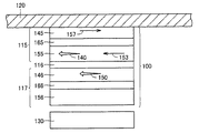
図3を参照して、トグルセルは、ビット線120とデジット線130との間に挟まれた薄膜磁性体100を有する。ビット線120およびデジット線130は、電流を通すことが可能な導電性材料を含む。この図では、ビット線120は、薄膜磁性体100の上部に位置付けられており、デジット線130は薄膜磁性体100の下部に位置付けられている。また、デジット線130は、ビット線120に対して90°の角度に方向づけられている。
Referring to FIG. 3, the toggle cell has a thin film
薄膜磁性体100は、第1の磁気部115と、トンネルバリア116と、第2の磁気部17とを含む。トンネルバリア116は、第1の磁気領域115と第2の磁気領域117との間に挟まれている。
The thin film
本例においては、第1の磁気部115は、3層構造で構成され、2つの強磁性体層145,155と、2つの強磁性体層145,155の間に挟まれた反強磁性体結合スペーサ層165とを有する。さらに、第2の磁気部117は、3層構造で形成され、2つの強磁性体層146,156と、2つの強磁性体層146,156の間に挟まれた反強磁性体結合スペーサ層166とを有する。
In the present example, the first
反強磁性体結合スペーサ層165および166は、例えば元素Ru、Os、Re、Cr、Rh、Cuのうちの少なくとも1つ、またはそれらの組合せを含む。さらに、強磁性体層145、155、146および156は、例えば元素Ni、Fe、Mn、Coのうちの少なくとも1つ、またはそれらの組合せを含む。また、第1の磁気部115および117は3層構造以外の合成反強磁性層材料構造を含む場合があり、たとえば、1つのそのような合成反強磁性層材料構造は、強磁性体層/反強磁性体結合スペーサ層/強磁性体層/反強磁性体結合スペーサ層/強磁性体層の構造で形成される5層の積層構造とすることも可能である。
Antiferromagnetic coupling spacer layers 165 and 166 include, for example, at least one of the elements Ru, Os, Re, Cr, Rh, Cu, or combinations thereof. Further, the
強磁性体層145および155は各々、反強磁性体結合スペーサ層165の結合によって通常時においては反平行に保たれた磁気モーメントベクトル157および153をそれぞれ有する。また、第1の磁気部115は合力磁気モーメントベクトル140を有し、第2の磁気部117は合力磁気モーメントベクトル150を有する。
The
合力磁気モーメントベクトル140および150は、磁化容易軸に沿って、ビット線120とデジット線130とに挟まれた間の所定角度、好ましくは45°,135°,225°,315°の方向に向けられているものとする。この点が通常のメモリセルと相違する。メモリセルにおいては、磁化容易軸はビット線方向となるように配置されていたが、トグルセルMCについては、磁化容易軸は、ビット線およびデジット線に挟まれた間において、所定角度ずれた位置となるように配置されているからである。
The resultant
さらに、第1の磁気部115は、自由な強磁性体領域すなわち自由磁化層であり、つまり、印加された磁界の存在下で合力磁気モーメントベクトル140が回転する。第2の磁気部117は、固定された一定の磁化方向を有する強磁性体領域すなわち固定磁化層であり、つまり、合力磁気モーメントベクトル150は適度に印加された磁界の存在下で自由に回転せず、基準層として使用される。
Furthermore, the first
反強磁性体結合層165は第1の磁気部115の2つの強磁性体層145,155の間に示されているが、強磁性体層は静磁場または他の特徴といった他の手段を介して反強磁性的に結合可能である。
Although the
なお、少なくとも強磁性体層145および155の作成において、好ましい磁化容易軸(誘導異方性)を設定するために磁界が提供される。提供された磁界は、磁気モーメントベクトル153および157にとって好ましい異方性軸を作り出す。好ましい軸は、これから説明されるように、ビット線120とデジット線130との間で45°の角度となるよう設定される。
Note that a magnetic field is provided to set a preferred easy axis of magnetization (inductive anisotropy) at least in the formation of the
図4は、本発明の実施の形態に従うトグルセルの磁化方向を説明する図である。 FIG. 4 is a diagram illustrating the magnetization direction of the toggle cell according to the embodiment of the present invention.
図4を参照して、トグルセルMCの薄膜磁性体100は、ビット線120およびデジット線130とが互いに90°の角度で交差する部分に設けられている。なお、説明を簡略化するため、図示されているようなx−y座標系と、時計回りの回転方向94および反時計回りの回転方向96とを参照することにする。
Referring to FIG. 4, thin film
そして、磁気モーメントベクトル153および157にとって好ましい異方性軸は、−x方向および−y方向に対して45°の角度、+x方向および+y方向に対して45°の角度で方向付けられている。一例として、図4は、磁気モーメントベクトル153が−x方向および−y方向に対して45°の角度で方向付けられていることを示している。磁気モーメントベクトル157は一般に、磁気モーメントベクトル153とは反平行に向けられているため、それは+x方向および+y方向に対して45°の角度で方向付けられている。
The preferred anisotropic axes for the
ビット線電流IWは円周方向の磁界HWを誘導し、デジット線電流Ipは円周方向のデジット磁界HDを誘導する。 The bit line current I W induces a circumferential magnetic field H W , and the digit line current I p induces a circumferential digit magnetic field H D.
ビット線120は、薄膜磁性体100の上部にあるため、素子の平面において、HWは、ビット線電流IWに対して+y方向に印加される。同様に、デジット線130は、薄膜磁性体100の下部にあるため、素子の平面において、HDは、デジット線電流Ipに対して+x方向に印加される。
Since the
次に、本発明の実施の形態1に従うトグルセルの書込方式について説明する。 Next, a toggle cell writing method according to the first embodiment of the present invention will be described.
トグル書込方法を用いる場合、電流の方向にかかわらず、同じ極性の電流パルスがビット線120およびデジット線130の双方に対して選択されている限り、薄膜磁性体100の自由磁化層の磁化方向は、書込動作毎にスイッチングされる。たとえば、「1」が最初に記憶されている場合、1つの電流パルスシーケンスがビット線およびデジット線を流れた後は「0」にスイッチングされる。そして、「0」が記憶されている場合、電流パルスシーケンスを繰り返せば、「1」に戻る。
When the toggle writing method is used, the magnetization direction of the free magnetic layer of the thin film
したがって、1回の書込シーケンスにより必ずデータレベルがこの書込シーケンス前に記憶されたデータレベルから反転したデータレベルへと変化する。 Therefore, the data level always changes from the data level stored before this writing sequence to the inverted data level by one writing sequence.
図5は、本発明の実施の形態に従うトグルセルの書込時における電流パルスシーケンスである。 FIG. 5 is a current pulse sequence during writing of the toggle cell according to the embodiment of the present invention.
ここでは、ビット線電流IWおよびデジット線電流Ipが示されており、その位相はデジット線電流Ipが90°位相遅れた波形が示されている。 Here, the bit line current I W and the digit line current I p are shown, and the phases thereof are shown as waveforms in which the digit line current I p is delayed by 90 °.
図6を用いて、図5で示されたパルスシーケンスを用いてトグルセルのデータ書込について説明する。 The toggle cell data writing will be described with reference to FIG. 6 using the pulse sequence shown in FIG.
ここで図6を参照して、本例においては、図5で示されたパルスシーケンスを用いて「1」を「0」に書込むためのトグル書込モードを示している。 Referring now to FIG. 6, in this example, a toggle write mode for writing “1” to “0” using the pulse sequence shown in FIG. 5 is shown.
この図では、時点t0で、磁気モーメントベクトル153および157は、図6に示すような好ましい方向に向けられている。この向きは「1」として定義される。
In this figure, at time t 0 ,
時刻t1で、ビット線電流IWがオンになり、それは磁界HWを+y方向に方向付けられるよう誘導する。磁界HWの効果は、ほぼバランスのとれた、反整列された第1の磁気部115の3層構造を「フロップ」させて、印加された磁界の方向に対して約90°に向けられるようにすることである。強磁性体層145および155間の有限の反強磁性体交換相互作用により、磁気モーメントベクトル153および157はここで、磁界の方向に向けて少しの角度それるようになり、合力磁気モーメントベクトル140は磁気モーメントベクトル153および157間の角度の範囲を定めて磁界HWと整列する。このため、磁気モーメントベクトル153は時計回りの方向94に回転する。合力磁気モーメントベクトル140は磁気モーメントベクトル153および157のベクトル加法であるため、磁気モーメントベクトル157も時計回りの方向94に回転する。
At time t 1 , the bit line current I W is turned on, which induces the magnetic field H W to be directed in the + y direction. The effect of the magnetic field H W is such that the nearly balanced, anti-aligned three-layer structure of the first
時刻t2で、デジット電流Ipがオンになり、それは磁界HDを誘導する。したがって、合力磁気モーメントベクトル140は、磁界HWによって+y方向に、磁界HDによって+x方向に同時に方向付けられ、それは、合力磁気モーメントベクトル140を、それが概して+x方向と+y方向との間の45°の角度に向けられるまで時計方向94にさらに回転させる効果を有する。したがって、磁気モーメントベクトル153および157も時計回りの方向94にさらに回転する。
In time t 2, the digit current I p turns on, it induces a magnetic field H D. Thus, the resultant
時刻t3で、ビット線電流IWがオフになり、そのためここでは磁界HDのみが合力磁気モーメントベクトル140を方向付け、それはここでは+x方向に向けられる。双方の磁気モーメントベクトル153および157はここでは概して、それらの磁化困難軸不安定点を通った角度に方向付けられる。
At time t 3, the bit line current I W is turned off, therefore direct the magnetic field H D only force
時刻t4で、デジット電流Ipがオフになり、そのため合力磁気モーメントベクトル140には磁界力が作用していない。したがって、磁気モーメントベクトル153および157は、それらの最も近い好ましい方向に向けられて、異方性エネルギーを最小限に抑える。この場合、磁気モーメントベクトル153にとって好ましい方向は、+y方向および+x方向に対して45°の角度である。この好ましい方向は、時刻t0での磁気モーメントベクトル153の最初の方向から180°でもあり、「0」として定義される。このため、薄膜磁性体100は既に「0」にスイッチングされている。
At time t 4 , the digit current I p is turned off, so that no magnetic force is acting on the resultant
図7を用いて、図5で示されたパルスシーケンスを用いてトグルセルの別のデータ書込について説明する。 With reference to FIG. 7, another data writing of the toggle cell will be described using the pulse sequence shown in FIG.
ここで図7を参照すると、本例においては、図5で示されたパルスシーケンスを用いて「0」を「1」に書込むためのトグル書込モードを示している。 Referring now to FIG. 7, in this example, a toggle write mode for writing “0” to “1” using the pulse sequence shown in FIG. 5 is shown.
図示されているのは、前述のような時刻t0、t1、t2、t3およびt4の各々での磁気モーメントベクトル153および157ならびに合力磁気モーメントベクトル140であり、薄膜磁性体の状態を同じ電流および磁界方向で「0」から「1」にスイッチングできることを示している。
Shown are the
図8は、本発明の実施の形態1に従うメモリセルMC0およびMC1の詳細を説明する回路構成図である。 FIG. 8 is a circuit configuration diagram illustrating details of memory cells MC0 and MC1 according to the first embodiment of the present invention.
本発明の実施の形態1に従うメモリセルMCは、複数のトンネル磁気抵抗素子TMRに対して1つのアクセストランジスタを共有した構成となっている。 Memory cell MC according to the first embodiment of the present invention has a configuration in which one access transistor is shared by a plurality of tunneling magneto-resistance elements TMR.
図8を参照して、本発明の実施の形態1に従うメモリセルMC0は、トンネル磁気抵抗素子TMR0〜TMR3と、アクセストランジスタATRとを含む。 Referring to FIG. 8, memory cell MC0 according to the first embodiment of the present invention includes tunneling magneto-resistance elements TMR0 to TMR3 and access transistor ATR.
トンネル磁気抵抗素子TMR0〜TMR3は、ビット線BL0とアクセストランジスタATRとの間にそれぞれ並列に接続されている。アクセストランジスタATRは、複数のトンネル磁気抵抗素子TMRを介してソース線SLとビット線BL0との間に配置され、そのゲートはワード線WL<0>と電気的に結合されている。 Tunneling magneto-resistance elements TMR0 to TMR3 are connected in parallel between bit line BL0 and access transistor ATR, respectively. Access transistor ATR is arranged between source line SL and bit line BL0 via a plurality of tunneling magneto-resistance elements TMR, and its gate is electrically coupled to word line WL <0>.
また、図8を参照して、メモリセルMC1も同様に構成されており、具体的には、トンネル磁気抵抗素子TMR0〜TMR3がアクセストランジスタATRとビット線BL1との間に並列にそれぞれ配置されている。また、アクセストランジスタATRは、複数のトンネル磁気抵抗素子を介してビット線BL1とソース線SLとの間に配置され、そのゲートはワード線WL<1>と電気的に結合されている。ここで、メモリセルMC0とMC1のソース線SLは互いに共有している。ソース線SLは、2行のメモリセル行毎に1本のソース線SLが設けられている。また、メモリセルMC0およびMC1において、トンネル磁気抵抗素子TMR0は、デジット線DL<0>を共有している。また、他のトンネル磁気抵抗素子TMR1〜3についても同様にメモリセルMC0、MC1でデジット線DL<1>〜DL<3>を共有した構成となっている。 Referring to FIG. 8, memory cell MC1 is similarly configured. Specifically, tunneling magneto-resistance elements TMR0 to TMR3 are arranged in parallel between access transistor ATR and bit line BL1, respectively. Yes. Access transistor ATR is arranged between bit line BL1 and source line SL via a plurality of tunnel magnetoresistive elements, and its gate is electrically coupled to word line WL <1>. Here, the source lines SL of the memory cells MC0 and MC1 are shared with each other. The source line SL is provided with one source line SL for every two memory cell rows. In memory cells MC0 and MC1, tunneling magneto-resistance element TMR0 shares digit line DL <0>. Similarly, the other tunnel magnetoresistive elements TMR1 to TMR3 share the digit lines DL <1> to DL <3> with the memory cells MC0 and MC1.
また、デジット線DL<0>〜DL<3>の一端側は、図示しないが電源電圧Vccと電気的に結合されており、他端側は固定電圧Vssと接続された複数のトランジスタ40が設けられている。そして、各トランジスタ40のゲートは、各デジット線DL<0>〜DL<3>にそれぞれ対応して行選択信号WD<0>〜WD<3>の入力を受けてオンし、デジット線DLにデータ書込電流が流れる。
Further, although not shown, one end side of the digit lines DL <0> to DL <3> is electrically coupled to the power supply voltage Vcc, and the other end side is provided with a plurality of
また、メモリセル行に沿った隣接する2つのメモリセルMC0,MC1でソース線SLを共有した構成であるため配線数を抑制して配線ピッチも十分に確保することが可能となる。 Further, since the source line SL is shared by two adjacent memory cells MC0 and MC1 along the memory cell row, it is possible to suppress the number of wirings and secure a sufficient wiring pitch.
また、隣接する2つのメモリセルMCのアクセストランジスタは互いに異なるワード線WL<0>およびWL<1>とそれぞれ電気的に結合されている。 Access transistors of two adjacent memory cells MC are electrically coupled to different word lines WL <0> and WL <1>, respectively.
図9は、本発明の実施の形態1に従うメモリセルMCの断面構成を説明する図である。 FIG. 9 is a diagram illustrating a cross-sectional configuration of memory cell MC according to the first embodiment of the present invention.
図9を参照して、半導体基板SUB上に形成されたアクセストランジスタATRは、n型領域であるソース/ドレイン領域310および320とゲート領域とを有する。
Referring to FIG. 9, access transistor ATR formed on semiconductor substrate SUB has source /
アクセストランジスタATRのゲートとなるワード線WLはp型のゲート領域の上層に形成される。 Word line WL serving as the gate of access transistor ATR is formed in an upper layer of the p-type gate region.
ソース/ドレイン領域310は、第1層の金属配線層350において形成されるソース線SLと電気的に結合される。デジット線DLは、第1層の金属配線層350の上層の第2層の金属配線層375に形成される。
Source /
トンネル磁気抵抗素子TMRは、デジット線DLの上層側に配置される。具体的には、デジット線DL<0>〜DL<3>のそれぞれ上層側にトンネル磁気抵抗素子TMR0〜TMR3が設けられる。また、トンネル磁気抵抗素子TMR0〜TMR3はストラップSTおよびコンタクトホール340に形成された金属膜を介してアクセストランジスタATRのソース/ドレイン領域320と電気的に結合される。ストラップSTは、トンネル磁気抵抗素子TMR0〜TMR3をアクセストランジスタATRと電気的に結合するために設けられ、導電性の物質で形成される。
Tunneling magneto-resistance element TMR is arranged on the upper layer side of digit line DL. Specifically, tunneling magneto-resistance elements TMR0 to TMR3 are provided on the upper layers of digit lines DL <0> to DL <3>, respectively. Tunnel magnetoresistive elements TMR0 to TMR3 are electrically coupled to source /
ビット線BLは、トンネル磁気抵抗素子TMR0〜TMR3とそれぞれ電気的に結合され、トンネル磁気抵抗素子TMR0〜TMR3の上層の第3層の金属配線層360に形成される。一方、ワード線WLは、アクセストランジスタATRのゲート電圧を制御するために設けられるので、電流を積極的に流す必要はない。したがって、集積度を高める観点から、ワード線WLは、独立した金属配線層を新たに設けることなく、ゲート330と同一の配線層にポリシリコン層やポリサイド層などを用いて形成されるのが一般的である。
Bit lines BL are electrically coupled to tunneling magneto-resistance elements TMR0 to TMR3, respectively, and are formed in third-layer
図10は、本発明の実施の形態1に従うメモリセルMCのレイアウトを説明する図である。ここでは、デバイス上部方向からデバイスを見た場合のレイアウト構成が示されている。 FIG. 10 shows a layout of memory cell MC according to the first embodiment of the present invention. Here, the layout configuration when the device is viewed from above is shown.
図10を参照して、ビット線BL0,BL1をそれぞれ形成する第3層の金属配線層360,361が上層に形成されている。トンネル磁気抵抗素子TMR0〜TMR3は、第3の金属配線層360,361と、ストラップSTとの間に挟まれている。そして、ストラップSTは、コンタクトホール340を介してn型領域であるソース/ドレイン領域320と結合される。また、ストラップSTの下においては、第2層の金属配線層375を用いてデジット線DL<0>〜DL<3>がトンネル磁気抵抗素子TMR0〜TMR3にそれぞれ対応して設けられている。そして、さらに下においては、ソース/ドレイン領域310,320を電気的に結合するワード線WLを形成するゲート330が設けられる。ここでは、メモリセルMC0に対応して設けられたワード線WL<0>と、メモリセルMC1に対応して設けられたワード線WL<1>が示されている。また、ソース/ドレイン領域310と電気的に結合されるソース線SLが第1層の金属配線層350を用いて形成される。
Referring to FIG. 10, third metal wiring layers 360 and 361 for forming bit lines BL0 and BL1 are formed in the upper layer. Tunneling magneto-resistance elements TMR0 to TMR3 are sandwiched between third metal wiring layers 360 and 361 and strap ST. Strap ST is coupled to source /
本発明の実施の形態に従う構成の如く複数のトンネル磁気抵抗素子TMRに対して1つのアクセストランジスタを共有した構成とすることにより、メモリセルの集積度を向上することができる。特にアクセストランジスタのサイズを小さくすることにより集積度の向上を図ることができるが、そのサイズの縮小には限度があり、セルピッチは、トンネル磁気抵抗素子のサイズではなく、アクセストランジスタのサイズに起因している場合が多い。したがって、アクセストランジスタのサイズに合わせて、トンネル磁気抵抗素子を複数個配置することによりエリアペナルティの小さい集積度の高い不揮発性記憶装置を実現することが可能である。
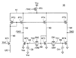
図11は、本発明の実施の形態1に従う比較部55の回路構成図である。
By using a configuration in which one access transistor is shared for a plurality of tunneling magneto-resistance elements TMR as in the configuration according to the embodiment of the present invention, the degree of integration of memory cells can be improved. In particular, it is possible to improve the degree of integration by reducing the size of the access transistor, but there is a limit to the reduction of the size, and the cell pitch is caused not by the size of the tunnel magnetoresistive element but by the size of the access transistor. There are many cases. Therefore, it is possible to realize a highly integrated nonvolatile memory device with a small area penalty by arranging a plurality of tunneling magnetoresistive elements in accordance with the size of the access transistor.
FIG. 11 is a circuit configuration diagram of
図11を参照して、本発明の実施の形態1に従う比較部55は、トランジスタPT1〜PT5と、トランジスタNT1〜NT4と、トランスファーゲートTG1,TG2と、キャパシタCA,CBとを含む。
Referring to FIG. 11,
トランジスタPT2は、ノードN1とノードN0との間に配置され、そのゲートはノードN0と電気的に結合される。トランジスタNT1は、ノードN0とデータ線DIOとの間に配置され、そのゲートは基準電圧Vrefの入力を受ける。この基準電圧Vrefは、データ線LIOを所定の電圧レベルに制御する制御電圧である。トランジスタPT1は、電源電圧VccとノードN1との間に配置され、そのゲートは制御信号/SAEの入力を受ける。トランジスタPT3は、ノードN1とノードN2との間に配置され、そのゲートはノードN0の入力を受ける。トランジスタPT4は、ノードN1とノードN3との間に配置され、そのゲートはノードN0と電気的に接続される。トランジスタPT5は、ノードN1とノードN4との間に配置され、そのゲートはノードN0と電気的に結合される。トランジスタNT2は、ノードN2と固定電圧Vssとの間に配置され、そのゲートはノードN5と電気的に結合される。 Transistor PT2 is arranged between nodes N1 and N0, and has its gate electrically coupled to node N0. Transistor NT1 is arranged between node N0 and data line DIO, and its gate receives input of reference voltage Vref. The reference voltage Vref is a control voltage for controlling the data line LIO to a predetermined voltage level. Transistor PT1 is arranged between power supply voltage Vcc and node N1, and has its gate receiving control signal / SAE. Transistor PT3 is arranged between nodes N1 and N2, and has its gate receiving input of node N0. Transistor PT4 is arranged between nodes N1 and N3, and has its gate electrically connected to node N0. Transistor PT5 is arranged between nodes N1 and N4, and has its gate electrically coupled to node N0. Transistor NT2 is arranged between node N2 and fixed voltage Vss, and has its gate electrically coupled to node N5.
キャパシタCBは、ノードN5と固定電圧Vssとの間に配置される。トランスファーゲートTG2は、ノードN5とノードN6との間に配置され、そのゲートには制御信号EN2,/EN2がそれぞれ入力される。トランジスタNT3は、ノードN3と固定電圧Vssとの間に配置され、そのゲートはノードN6と電気的に結合される。トランスファーゲートTG1は、ノードN6とノードN8との間に配置され、そのゲートはそれぞれ制御信号EN1,/EN1の入力を受ける。キャパシタCAは、ノードN8と固定電圧Vssとの間に配置される。トランジスタNT4は、ノードN4と固定電圧Vssとの間に配置されそのゲートはノードN8と電気的に結合される。 Capacitor CB is arranged between node N5 and fixed voltage Vss. Transfer gate TG2 is arranged between nodes N5 and N6, and control signals EN2 and / EN2 are input to the gates, respectively. Transistor NT3 is arranged between node N3 and fixed voltage Vss, and has its gate electrically coupled to node N6. Transfer gate TG1 is arranged between nodes N6 and N8, and the gates receive control signals EN1 and / EN1, respectively. Capacitor CA is arranged between node N8 and fixed voltage Vss. Transistor NT4 is arranged between node N4 and fixed voltage Vss, and has its gate electrically coupled to node N8.
本発明の実施の形態に従う比較部55は、メモリセルを流れる通過電流に基づいてキャパシタCA,CBで電荷を蓄積し、キャパシタCA,CBで蓄積した電荷に基づいた比較データSAO,/SAOを増幅部210に出力する。
以下、具体的な動作について説明する。 A specific operation will be described below.
データ読出時において、まず制御信号/SAEが「L」レベルに設定される。これによりトランジスタPT1がオンし、電源電圧VccがノードN1と電気的に結合される。これにより、動作電圧が供給されデータ読出が実行される。そして、まず制御信号EN1、/EN1がそれぞれ「H」レベルおよび「L」レベルに設定される。一方、後述するが最初のデータ読出においては、制御信号EN2,/EN2は「L」レベルおよび「H」レベルに設定されている。すなわち、トランスファーゲートTG1はオンしており、ノードN6とノードN8とは電気的に結合されている。一方、トランスファーゲートTG2はオフであり、ノードN5とノードN6とは電気的に切離されている。 At the time of data reading, control signal / SAE is first set to “L” level. Thereby, transistor PT1 is turned on, and power supply voltage Vcc is electrically coupled to node N1. As a result, the operating voltage is supplied and data reading is executed. First, the control signals EN1 and / EN1 are set to the “H” level and the “L” level, respectively. On the other hand, as will be described later, in the first data reading, control signals EN2 and / EN2 are set to the “L” level and the “H” level. That is, transfer gate TG1 is on, and node N6 and node N8 are electrically coupled. On the other hand, the transfer gate TG2 is off, and the node N5 and the node N6 are electrically disconnected.
この状態において、データ線LIOを介して選択メモリセルに電流が供給されると、トランジスタPT2,PT4でカレントミラー回路が構成されているため同じ電流量が流れる。また、上述したようにノードN6とノードN8は電気的に結合されており、トランジスタNT3,NT4もカレントミラー回路を構成しているため同じ電流量が流れる。したがって、キャパシタCAには、最初のデータ読出においてデータ線LIOに流れる電流に基づいた電荷が蓄積される。 In this state, when a current is supplied to the selected memory cell via the data line LIO, the same amount of current flows because the transistors PT2 and PT4 form a current mirror circuit. Further, as described above, the node N6 and the node N8 are electrically coupled, and the transistors NT3 and NT4 also constitute a current mirror circuit, so that the same amount of current flows. Therefore, charge based on the current flowing through data line LIO in the first data read is stored in capacitor CA.
一方、2回目のデータ読出においては、制御信号EN2,/EN2は「H」レベルおよび「L」レベルに設定され、制御信号EN1,/EN1は「L」レベルおよび「H」レベルに設定される。すなわち、トランスファーゲートTG2はオンしており、ノードN5とノードN6とは電気的に結合されている。一方、トランスファーゲートTG1はオフであり、ノードN6とノードN8とは電気的に切離されている。
On the other hand, in the second data read, control signals EN 2 and /
この状態において、データ線LIOを介して選択メモリセルに電流が供給されると、トランジスタPT2,PT4でカレントミラー回路が構成されているため同じ電流量が流れる。また、上述したようにノードN5とノードN6とは電気的に結合されており、トランジスタNT2,NT3もカレントミラー回路を構成しているため同じ電流量が流れる。したがって、キャパシタCBには、2回目のデータ読出においてデータ線LIOに流れる電流に基づいた電荷が蓄積される。 In this state, when a current is supplied to the selected memory cell via the data line LIO, the same amount of current flows because the transistors PT2 and PT4 form a current mirror circuit. Further, as described above, the node N5 and the node N6 are electrically coupled, and the transistors NT2 and NT3 also constitute a current mirror circuit, so that the same amount of current flows. Therefore, the capacitor CB accumulates charges based on the current flowing through the data line LIO in the second data read.
そして、このキャパシタCA,CBに蓄積された電荷に基づいてトランジスタNT2,NT4がオンし、比較に応じた比較データ信号SAO,/SAOから出力する。 The transistors NT2 and NT4 are turned on based on the charges accumulated in the capacitors CA and CB, and are output from the comparison data signals SAO and / SAO corresponding to the comparison.
図12は、本発明の実施の形態1に従う増幅部60の回路構成図である。
FIG. 12 is a circuit configuration diagram of amplifying
増幅部60は、トランジスタPT6,PT7,PT10,PT11と、トランジスタNT5〜NT10とを含む。トランジスタNT8〜NT10は、ノードN9およびノードN10を短絡するために設けられている。トランジスタNT8は、ノードN9とノードN10との間に配置され、そのゲートは制御信号PRの入力を受ける。トランジスタNT9は、ノードN10と固定電圧Vssとの間に配置され、そのゲートは制御信号PRの入力を受ける。トランジスタNT10は、ノードN9と固定電圧Vssとの間に配置され、そのゲートは制御信号PRの入力を受ける。
Amplifying
制御信号PRが「H」レベルの場合にトランジスタNT8〜NT10が全てオンし、ノードN9およびN10が短絡されるとともに、固定電圧と結合されて放電される。 When control signal PR is at "H" level, all of transistors NT8-NT10 are turned on, nodes N9 and N10 are short-circuited, and are combined with a fixed voltage and discharged.
トランジスタPT7は、ノードN2とノードN10との間に配置され、そのゲートは制御信号PAEの入力を受ける。また、トランジスタPT6は、ノードN4とノードN9との間に配置され、そのゲートは制御信号PAEの入力を受ける。トランジスタPT6,PT7は、制御信号PAEが「L」レベルの場合にオンし、比較部55と増幅部60とを電気的に結合させる。
Transistor PT7 is arranged between nodes N2 and N10, and has its gate receiving control signal PAE. Transistor PT6 is arranged between nodes N4 and N9, and its gate receives control signal PAE. The transistors PT6 and PT7 are turned on when the control signal PAE is at "L" level, and electrically connects the
一方、制御信号PAEが「H」レベルである場合には、これらのトランジスタはオフとなり、比較部55と増幅部60とは電気的に切離された状態となる。
On the other hand, when the control signal PAE is at “H” level, these transistors are turned off, and the
アンプAMPは、いわゆるクロスラッチ型のセンスアンプであり、ノードN9およびノードN10に伝達された信号を増幅して、読出データDO,/DOとして出力する。 Amplifier AMP is a so-called cross-latch type sense amplifier, which amplifies signals transmitted to node N9 and node N10 and outputs them as read data DO, / DO.
アンプAMPは、トランジスタPT9〜PT11と、トランジスタNT5〜NT7とを含む。トランジスタPT9は、電源電圧VccとノードN11との間に配置され、そのゲートは制御信号/PAEの入力を受ける。制御信号/PAEは、制御信号PAEの反転信号である。トランジスタPT10は、ノードN11とノードN9との間に配置され、そのゲートはノードN10の入力を受ける。トランジスタPT11は、ノードN11とノードN10との間に配置され、そのゲートはノードN9の入力を受ける。トランジスタNT5は、ノードN9とノードN12との間に配置され、そのゲートはノードN10の入力を受ける。トランジスタNT6は、ノードN10とノードN12との間に配置され、そのゲートはノードN9と電気的に結合される。トランジスタNT7は、ノードN12と固定電圧Vssとの間に配置され、そのゲートは制御信号PAEの入力を受ける。 Amplifier AMP includes transistors PT9 to PT11 and transistors NT5 to NT7. Transistor PT9 is arranged between power supply voltage Vcc and node N11, and has its gate receiving control signal / PAE. Control signal / PAE is an inverted signal of control signal PAE. Transistor PT10 is arranged between nodes N11 and N9, and its gate receives the input of node N10. Transistor PT11 is arranged between nodes N11 and N10, and has its gate receiving the input of node N9. Transistor NT5 is arranged between nodes N9 and N12, and has its gate receiving the input of node N10. Transistor NT6 is arranged between nodes N10 and N12, and has its gate electrically coupled to node N9. Transistor NT7 is arranged between node N12 and fixed voltage Vss, and has its gate receiving control signal PAE.
データ読出前において、制御信号PAEは「L」レベルに設定されており、ノードN9およびノードN10は等電位に設定されている。そして、データ読出時において制御信号PAEは「H」レベルに設定され、ノードN9とノードN10とは切離されるとともにアンプAMPが活性化されて、ノードN9,N10に伝達された比較データ信号SAO,/SAOを増幅して読出データDO,/DOとして出力する。 Before data reading, control signal PAE is set to “L” level, and nodes N9 and N10 are set to the same potential. At the time of data reading, control signal PAE is set to "H" level, node N9 and node N10 are disconnected from each other, amplifier AMP is activated, and comparison data signals SAO, / SAO is amplified and output as read data DO and / DO.
図13は、本発明の実施の形態1に従うデータ読出動作を説明するフローチャート図である。 FIG. 13 is a flowchart illustrating a data read operation according to the first embodiment of the present invention.
本実施の形態1においては、選択対象となるメモリセルにおける1ビットのデータ読出について説明する。以下においては、一例としてメモリセルMC0に含まれる複数のトンネル磁気抵抗素子TMR0〜TMR3について主にトンネル磁気抵抗素子TMR0に着目して説明する。 In the first embodiment, 1-bit data reading in a memory cell to be selected will be described. Hereinafter, as an example, a plurality of tunnel magnetoresistive elements TMR0 to TMR3 included in the memory cell MC0 will be described mainly focusing on the tunnel magnetoresistive element TMR0.
データ読出動作が開始され(ステップS1)、初期データ読出動作が実行される(ステップS2)。具体的には、選択メモリセルの選択対象となるトンネル磁気抵抗素子から記憶データを読出して記憶データに応じた電荷をキャパシタCAに蓄積する。具体的には、ワード線WLが活性化(「H」レベル)されてソース線SLとビット線BL0との間で電流経路が形成される。また、読出選択信号RCSLが「H」レベルに設定され、ビット線BLとデータ線LIOとが電気的に結合されて、データ読出回路RDCからトンネル磁気抵抗素子の記憶データに応じた通過電流が供給される。 A data read operation is started (step S1), and an initial data read operation is executed (step S2). Specifically, the stored data is read from the tunnel magnetoresistive element to be selected for the selected memory cell, and the electric charge corresponding to the stored data is stored in the capacitor CA. Specifically, the word line WL is activated (“H” level), and a current path is formed between the source line SL and the bit line BL0. Further, read selection signal RCSL is set to “H” level, bit line BL and data line LIO are electrically coupled, and a passing current corresponding to the data stored in the tunnel magnetoresistive element is supplied from data read circuit RDC. Is done.
図14は、本発明の実施の形態1に従うメモリセルのトンネル磁気抵抗素子TMR0(高抵抗RH)のデータ読出を説明する図である。 FIG. 14 is a diagram illustrating data reading of tunneling magneto-resistance element TMR0 (high resistance RH) of the memory cell according to the first embodiment of the present invention.
本例においては、たとえば選択メモリセルの選択対象となるトンネル磁気抵抗素子としてトンネル磁気抵抗素子TMR0に着目する。 In this example, attention is focused on the tunnel magnetoresistive element TMR0 as a tunnel magnetoresistive element to be selected for the selected memory cell.
具体的には、データ読出時において、ビット線BLに所定電圧が印加され、各トンネル磁気抵抗素子TMR0〜TMR3にそれぞれ各トンネル磁気抵抗素子が有する抵抗値に応じた通過電流が流れる。たとえば、高抵抗RHを有するトンネル磁気抵抗素子TMR0に流れる電流をI0とする。そして、トンネル磁気抵抗素子TMR1〜TMR3に流れる電流をIAとする。この場合、全体としてメモリセルMCには、電流IA+I0が流れることになる。そして、比較部55は、上述したようにこの流れる電流IA+I0に対応した電荷をキャパシタCAに蓄積する。
Specifically, at the time of data reading, a predetermined voltage is applied to the bit line BL, and a passing current corresponding to the resistance value of each tunneling magneto-resistance element flows through each of the tunneling magneto-resistance elements TMR0 to TMR3. For example, the current flowing through tunneling magneto-resistance element TMR0 having high resistance RH is I0. The current flowing through tunneling magneto-resistance elements TMR1 to TMR3 is IA. In this case, the current IA + I0 flows through the memory cell MC as a whole. Then, as described above, the
再び、図13を参照して、次に、書込動作として選択メモリセルの選択対象となるトンネル磁気抵抗素子へ反転データを書込む(ステップS3)。具体的には、上述したように所定のパルスシーケンスで選択対象となるトンネル磁気抵抗素子に所定のデータ書込磁界を印加する。これにより、上述したようにトンネル磁気抵抗素子の自由層は、書込前の磁化方向と反対の磁化方向を有する。したがって、上述の図14で説明したトンネル磁気抵抗素子TMR0については、その磁化方向が反転して抵抗が低抵抗RLとなる。 Referring to FIG. 13 again, next, inversion data is written to the tunnel magnetoresistive element to be selected for the selected memory cell as a write operation (step S3). Specifically, as described above, a predetermined data write magnetic field is applied to the tunnel magnetoresistive element to be selected in a predetermined pulse sequence. Thereby, as described above, the free layer of the tunnel magnetoresistive element has a magnetization direction opposite to the magnetization direction before writing. Therefore, with respect to tunneling magneto-resistance element TMR0 described with reference to FIG. 14, the magnetization direction is reversed and the resistance becomes low resistance RL.
そして、次にデータ読出動作を実行する(ステップS4)。具体的には、選択メモリセルの選択対象となるトンネル磁気抵抗素子から反転データを読出して、反転データに応じた電荷をキャパシタCBに蓄積する。 Next, a data read operation is executed (step S4). Specifically, the inverted data is read from the tunnel magnetoresistive element to be selected for the selected memory cell, and the electric charge corresponding to the inverted data is accumulated in the capacitor CB.
図15は、本発明の実施の形態1に従うメモリセルのトンネル磁気抵抗素子TMR0(低抵抗RL)のデータ読出を説明する図である。 FIG. 15 is a diagram illustrating data reading of tunneling magneto-resistance element TMR0 (low resistance RL) of the memory cell according to the first embodiment of the present invention.
本例においては、たとえば選択メモリセルの選択対象となるトンネル磁気抵抗素子としてトンネル磁気抵抗素子TMR0に着目する。 In this example, attention is focused on the tunnel magnetoresistive element TMR0 as a tunnel magnetoresistive element to be selected for the selected memory cell.
データ読出時において、ビット線BLに所定電圧が印加され、各トンネル磁気抵抗素子TMR0〜TMR3にそれぞれ各トンネル磁気抵抗素子が有する抵抗値に応じた通過電流が流れる。したがって、トンネル磁気抵抗素子TMR0に流れる電流は上述したようにI1である。そして、トンネル磁気抵抗素子TMR1〜TMR3に流れる電流はIAである。この場合、全体としてメモリセルMCには、電流IA+I1が流れることになる。 At the time of data reading, a predetermined voltage is applied to the bit line BL, and a passing current corresponding to the resistance value of each tunnel magnetoresistive element flows through each of the tunnel magnetoresistive elements TMR0 to TMR3. Therefore, the current flowing through tunneling magneto-resistance element TMR0 is I1 as described above. The current flowing through tunneling magneto-resistance elements TMR1 to TMR3 is IA. In this case, the current IA + I1 flows through the memory cell MC as a whole.
一般的にトンネル磁気抵抗素子TMRのMR比は20%程ある。したがって、上述の反転データのデータ書込により、電流I0および電流I1については、このMR比に応じた電流変化を検出することができる。すなわち、データ読出マージンを十分に確保することが可能となる。 Generally, the MR ratio of the tunnel magnetoresistive element TMR is about 20%. Therefore, the current change corresponding to the MR ratio can be detected for current I0 and current I1 by the above-described data writing of the inverted data. That is, a sufficient data read margin can be secured.
そして、比較部55は、上述したようにこの流れる電流IA+I1に対応した電荷をキャパシタCBに蓄積する。
Then, as described above, the
そして、次に読出データ確定動作を実行する(ステップS5)。具体的には、キャパシタCAとCBとに蓄積された電荷に基づいて読出データDOを確定する。具体的には、データ読出回路RDCにおいて、上述した所定動作を実行することにより読出データDOが出力される。 Next, a read data determination operation is executed (step S5). Specifically, read data DO is determined based on the charges accumulated in capacitors CA and CB. Specifically, read data DO is output by executing the above-described predetermined operation in data read circuit RDC.
そして、次に書込動作を実行する(ステップS6)。具体的には、選択メモリセルの選択対象となるトンネル磁気抵抗素子へ記憶データを書戻す。これによりデータ読出動作を終了する(ステップS7)。 Next, a writing operation is executed (step S6). Specifically, the stored data is written back to the tunnel magnetoresistive element to be selected for the selected memory cell. Thereby, the data reading operation is finished (step S7).
図16は、本発明の実施の形態1に従うデータ読出動作のタイミングチャート図である。上述の一連のデータ読出動作について具体的に説明する。 FIG. 16 is a timing chart diagram of a data read operation according to the first embodiment of the present invention. The series of data reading operations described above will be specifically described.
まず、時刻t0において、最初の初期データ読出動作(1STリード)が開始される。具体的には、制御信号PRが「H」レベルから「L」レベルに設定される。これに伴い、ノードN9およびN10のイコライズおよび放電が終了し、ノードN9およびノードN10は電気的に切離される。また、制御信号SAE、ワード線WLおよび読出選択信号RCSLが活性化(「H」レベル)される。具体的には、ワード線WL(「H」レベル)によりアクセストランジスタATRがオンして、トンネル磁気抵抗素子TMRを介してビット線BLとソース線SLとが電気的に結合される。また、読出選択信号RCSKL(「H」レベル)によりビット線BLとデータ線LIOとが電気的に結合される。また、制御信号SAEが「H」レベルすなわち制御信号/SAEが「L」レベルに設定され、電源電圧Vccが比較部55に供給される。すなわち、トンネル磁気抵抗素子TMRを介して電源電圧Vccと固定電圧Vssとの間で電流経路が形成される。したがって、トンネル磁気抵抗素子TMRの抵抗値に応じた通過電流が流れる。そして、制御信号EN1が「H」レベルに設定され、通過電流に応じた電荷がキャパシタCAに蓄積される。たとえば、トンネル磁気抵抗素子TMRが低抵抗RH(「L」データ)の場合には、電流IA+I1が流れる。この電流量に応じた電荷がキャパシタCAに蓄積されてノードN8の電位が設定される。一方、トンネル磁気抵抗素子TMRが高抵抗RH(「H」データ)の場合には、電流IA+I0が流れる。この電流量に応じた電荷がキャパシタCAに蓄積されてノードN8の電位が設定される。
First, at time t0, an initial initial data read operation (1ST read) is started. Specifically, the control signal PR is set from the “H” level to the “L” level. Accordingly, equalization and discharge of nodes N9 and N10 are completed, and nodes N9 and N10 are electrically disconnected. Control signal SAE, word line WL and read selection signal RCSL are activated ("H" level). Specifically, access transistor ATR is turned on by word line WL (“H” level), and bit line BL and source line SL are electrically coupled via tunneling magneto-resistance element TMR. Further, bit line BL and data line LIO are electrically coupled to each other by read selection signal RCSKL (“H” level). Further, the control signal SAE is set to the “H” level, that is, the control signal / SAE is set to the “L” level, and the power supply voltage Vcc is supplied to the
次に、時刻t1において、書込動作(1STライト)が実行される。具体的には、上述した所定のパルスシーケンスにより選択対象となるトンネル磁気抵抗素子TMRのデータが反転する。 Next, at time t1, a write operation (1ST write) is executed. Specifically, the data of the tunnel magnetoresistive element TMR to be selected is inverted by the predetermined pulse sequence described above.
そして、時刻t2において、2回目のデータ読出動作(2STリード)が実行される。具体的には、上述したようにトンネル磁気抵抗素子TMRを介して電源電圧Vccと固定電圧Vssとの間で電流経路が形成される。したがって、トンネル磁気抵抗素子TMRの抵抗値に応じた通過電流が流れる。そして、制御信号EN2が「H」レベルに設定され、通過電流に応じた電荷がキャパシタCBに蓄積される。たとえば、反転してトンネル磁気抵抗素子TMRが低抵抗RL(「H」データ)の場合には、電流IA+I0が流れる。この電流量に応じた電荷がキャパシタCBに蓄積されてノードN5の電位が設定される。一方、反転してトンネル磁気抵抗素子TMRが高抵抗RH(「L」データ)の場合には、電流IA+I1が流れる。この電流量に応じた電荷がキャパシタCBに蓄積されてノードN5の電位が設定される。 At time t2, the second data read operation (2ST read) is performed. Specifically, as described above, a current path is formed between the power supply voltage Vcc and the fixed voltage Vss via the tunnel magnetoresistive element TMR. Therefore, a passing current corresponding to the resistance value of tunneling magneto-resistance element TMR flows. Then, the control signal EN2 is set to the “H” level, and the electric charge corresponding to the passing current is accumulated in the capacitor CB. For example, when tunneling magneto-resistance element TMR is low resistance RL (“H” data) after inversion, current IA + I0 flows. Charge corresponding to the amount of current is accumulated in the capacitor CB, and the potential of the node N5 is set. On the other hand, when tunneling magneto-resistance element TMR is high resistance RH (“L” data), current IA + I1 flows. Charge corresponding to the amount of current is accumulated in the capacitor CB, and the potential of the node N5 is set.
そして、キャパシタCAおよびCBに蓄積された電荷に従って、すなわちノードN5およびN8の電位に従って比較データ信号SAO,/SAOが増幅されて増幅部60に伝達される。そして、時刻t3の前において、制御信号PAE(「H」レベル)に応答してアンプAMPにおいて増幅動作が実行される。これにより読出データDOが出力される。トンネル磁気抵抗素子TMRの記憶データが「L」データの場合には、ノードN8の方がノードN5よりも電位レベルが高いので比較データSAO,/SAOは「L」レベルおよび「H」レベルにそれぞれ設定される。そして、後段の増幅部60でさらに増幅されて読出データDO,/DOは「L」レベルおよび「H」レベルにそれぞれ設定される。一方、トンネル磁気抵抗素子TMRの記憶データが「H」データの場合には、ノードN8の方がノードN5の電位レベルよりも低いので比較データSAO,/SAOは「L」レベルおよび「L」レベルにそれぞれ設定される。そして、後段の増幅部60でさらに増幅されて読出データDO,/DOは「L」レベルおよび「L」レベルにそれぞれ設定される。
Then, the comparison data signals SAO and / SAO are amplified according to the electric charges stored in the capacitors CA and CB, that is, according to the potentials of the nodes N5 and N8, and transmitted to the amplifying
時刻t3において、読出データ確定動作とともに書込動作(2NDライト)が実行される。 At time t3, the write operation (2ND write) is executed together with the read data determination operation.
具体的には、前の書込動作によりデータが反転しているため、再度書込動作を実行することにより元の記憶データに再現することが可能となる。 Specifically, since the data has been inverted by the previous write operation, it is possible to reproduce the original stored data by executing the write operation again.
これにより、選択メモリセルの選択対象となるトンネル磁気抵抗素子のデータ読出を実行することができる。すなわち、1ビットのデータ読出を実行することができる。 Thereby, data reading of the tunnel magnetoresistive element to be selected by the selected memory cell can be executed. That is, 1-bit data reading can be executed.
図17は、本発明の実施の形態1に従うデータ書込動作を説明するフローチャート図である。 FIG. 17 is a flowchart illustrating a data write operation according to the first embodiment of the present invention.
図17を参照して、データ書込動作を開始する(ステップS10)。この場合には、最初の記憶データが「0」もしくは「1」のいずれであるかを判別する必要がある。したがって、初期データ読出動作(ステップS11)、書込動作(ステップS12)、データ読出動作(ステップS13)および読出データ確定動作(ステップS14)については、上述したステップS2〜S5で説明したのと同様であるのでその詳細な説明は繰返さない。 Referring to FIG. 17, the data writing operation is started (step S10). In this case, it is necessary to determine whether the first stored data is “0” or “1”. Therefore, the initial data read operation (step S11), write operation (step S12), data read operation (step S13), and read data determination operation (step S14) are the same as described in steps S2 to S5 described above. Therefore, detailed description thereof will not be repeated.
次に、ステップS15において、読出データDOと、書込データとが一致するかどうかを判定する。一致する場合には、書込動作を実行する(ステップS16)。 Next, in step S15, it is determined whether or not the read data DO and the write data match. If they match, the writing operation is executed (step S16).
一方、ステップS15において、読出データDOと書込データとが一致しない場合にはスキップしてデータ書込動作を終了する(ステップS17)。 On the other hand, if the read data DO and the write data do not match in step S15, the data write operation is terminated by skipping (step S17).
一致する場合に、書込動作を実行するのは、現在のトンネル磁気抵抗素子のデータレベルが前の書込動作(ステップS12)により反転データとなっているため元の記憶データに戻す必要があるからである。 If they match, the write operation is executed because the data level of the current tunnel magnetoresistive element has been inverted by the previous write operation (step S12), so it is necessary to restore the original stored data. Because.
一方、一致しない場合に、書込動作(ステップS16)をスキップするのは、現在のトンネル磁気抵抗素子のデータレベルが前の書込動作(ステップS12)により反転データとなっているためさらに書込動作(ステップS16)を実行する必要がないからである。これにより、無駄な書込動作を停止して消費電力を低減することができる。 On the other hand, if they do not match, the write operation (step S16) is skipped because the data level of the current tunnel magnetoresistive element is inverted data due to the previous write operation (step S12). This is because it is not necessary to execute the operation (step S16). Thereby, useless writing operation can be stopped and power consumption can be reduced.
上記で説明したように本願実施の形態1に従うデータ読出方式およびデータ書込方式により、複数のトンネル磁気抵抗素子に対してアクセストランジスタを共有するトグルセルに対してもセルフリファレンスのデータ読出およびデータ書込を実行することができる。 As described above, self-reference data reading and data writing are performed even for a toggle cell sharing an access transistor for a plurality of tunnel magnetoresistive elements by the data reading method and data writing method according to the first embodiment of the present application. Can be executed.
(実施の形態1の変形例)
上記の実施の形態1においては、一つのメモリセルにおいて、複数のトンネル磁気抵抗素子TMRが互いに並列に同じ位置に設けられた構造を例に挙げて説明した。
(Modification of Embodiment 1)
In the first embodiment, the structure in which a plurality of tunnel magnetoresistive elements TMR are provided in parallel at the same position in one memory cell has been described as an example.
本発明の実施の形態1の変形例においては、複数のトンネル磁気抵抗素子が積層された
構造について説明する。
In the modification of the first embodiment of the present invention, a structure in which a plurality of tunnel magnetoresistive elements are stacked will be described.
図18は、本発明の実施の形態1に従うメモリセルMC♯およびその周辺回路を説明する図である。 FIG. 18 is a diagram illustrating memory cell MC # and its peripheral circuit according to the first embodiment of the present invention.
図18を参照して、メモリセルMC#は、複数のトンネル磁気抵抗素子TMR0〜TMR3と、アクセストランジスタATRとを含む。また、ここではトンネル磁気抵抗素子TMRを積層した場合の回路構成図が示されている。トンネル磁気抵抗素子TMR0〜TMR3にそれぞれ対応して、データ書込電流が流れる書込ビット線WBL0〜WBL3およびデジット線DL0〜DL3が設けられている。 Referring to FIG. 18, memory cell MC # includes a plurality of tunneling magneto-resistance elements TMR0 to TMR3 and an access transistor ATR. Here, a circuit configuration diagram in the case where the tunnel magnetoresistive elements TMR are stacked is shown. Corresponding to tunneling magneto-resistance elements TMR0 to TMR3, write bit lines WBL0 to WBL3 and digit lines DL0 to DL3 through which a data write current flows are provided.
またトンネル磁気抵抗素子TMR0〜TMR3に共通にアクセストランジスタATRが設けられており、ゲートはワード線WLと電気的に結合されている。ワード線WLの活性化に応答してアクセストランジスタはオンし、リードビット線RBLと各トンネル磁気抵抗素子TMRとが電気的に結合される。 An access transistor ATR is provided in common to tunneling magneto-resistance elements TMR0 to TMR3, and a gate is electrically coupled to word line WL. In response to activation of word line WL, the access transistor is turned on, and read bit line RBL and each tunnel magnetoresistive element TMR are electrically coupled.
また、書込ビット線WBL0〜WBL3の一端側は、書込ビット線WBL0〜WBL3をプルアップするためのドライバトランジスタTr0#,Tr2#,Tr4#,Tr6#がそれぞれ設けられている。そして、ドライバトランジスタTr0#,Tr2#,Tr4#,Tr6#のゲートには、それぞれ書込制御信号WCSL<0>〜WCSL<3>がそれぞれ入力されている。また、書込ビット線WBL0〜WBL3の他端側は固定電圧Vssと電気的に結合されている。たとえば、書込制御信号WCSL<1>が「H」レベルの場合には、ドライバトランジスタTr0#がオンして、書込ビット線WBL0にデータ書込電流が流れる。 Further, driver transistors Tr0 #, Tr2 #, Tr4 #, Tr6 # for pulling up the write bit lines WBL0 to WBL3 are provided on one end side of the write bit lines WBL0 to WBL3, respectively. The write control signals WCSL <0> to WCSL <3> are input to the gates of the driver transistors Tr0 #, Tr2 #, Tr4 #, Tr6 #, respectively. The other end side of write bit lines WBL0-WBL3 is electrically coupled to fixed voltage Vss. For example, when write control signal WCSL <1> is at “H” level, driver transistor Tr0 # is turned on and a data write current flows through write bit line WBL0.
また、リードビット線RBLは、メモリセル列にそれぞれ対応して設けられ、読出選択ゲートRCSG0を介してデータ線LIOと電気的に結合されている。読出選択ゲートRCSG0は、列選択信号RCSL<0>に応答してリードビット線RBLとデータ線LIOとを電気的に結合する。データ線LIOは、データ読出回路RDCと接続されている。データ読出回路RDCについては、実施の形態1で説明したのと同様であるのでその詳細な説明は繰り返さない。 Read bit line RBL is provided corresponding to each memory cell column, and is electrically coupled to data line LIO via read select gate RCSG0. Read select gate RCSG0 electrically couples read bit line RBL and data line LIO in response to column select signal RCSL <0>. Data line LIO is connected to data read circuit RDC. Since data read circuit RDC is the same as that described in the first embodiment, detailed description thereof will not be repeated.
図19は、図18で説明したメモリセルMC♯の断面を説明する図である。 FIG. 19 is a diagram illustrating a cross section of memory cell MC # described in FIG.
図19を参照して、メモリセルMC#は、トンネル磁気抵抗素子TMRを含むセルユニットCUで構成される。具体的には、本例においては、各トンネル磁気抵抗素子TMR0〜TMR3をそれぞれ含むセルユニットCU0〜CU3が示されている。すなわち、各セルユニットCUが一段ずつ積層されている構成が示されている。 Referring to FIG. 19, memory cell MC # is formed of a cell unit CU including tunneling magneto-resistance element TMR. Specifically, in this example, cell units CU0 to CU3 including the respective tunnel magnetoresistive elements TMR0 to TMR3 are shown. That is, a configuration in which each cell unit CU is stacked one by one is shown.
半導体基板SUB上に形成されたアクセストランジスタATRは、n型領域であるソース/ドレイン領域310および320とゲート領域とを有する。
Access transistor ATR formed on semiconductor substrate SUB has source /
アクセストランジスタATRのゲートとなるワード線WLはp型のゲート領域の上層に形成される。 Word line WL serving as the gate of access transistor ATR is formed in an upper layer of the p-type gate region.
ソース/ドレイン領域320は、第1層の金属配線層350において形成されるリードビット線RBLとコンタクトホール351を介して電気的に結合される。ソース/ドレイン領域310は、コンタクトホール340を介して上層のセルユニットCU0〜CU3と電気的に結合される。ワード線WLは、アクセストランジスタATRのゲート電圧を制御するために設けられるので、電流を積極的に流す必要はない。したがって、集積度を高める観点から、ワード線WLは、金属配線層を新たに設けることなく、ゲート330と同一の配線層にポリシリコン層やポリサイド層などを用いて形成されるのが一般的である。
Source /
セルユニットCUは、トンネル磁気抵抗素子TMRと、書込ビット線WBLと、デジット線DLとで構成される。具体的には、第2層の金属配線層360にデジット線DLが設けられる。セルユニットCU0において、トンネル磁気抵抗素子TMR0は、デジット線DL0の上層側に配置される。また、トンネル磁気抵抗素子TMR0は、ストラップSTおよびコンタクトホール340に形成された金属膜を介してアクセストランジスタATRのソース/ドレイン領域310と電気的に結合される。ストラップSTは、トンネル磁気抵抗素子TMR0〜TMR3をアクセストランジスタATRと電気的に結合するために設けられ、導電性の物質で形成される。また、書込ビット線WBLは、第3層の金属配線層370に設けられ、トンネル磁気抵抗素子TMR0と電気的に結合される。
Cell unit CU includes tunneling magneto-resistance element TMR, write bit line WBL, and digit line DL. Specifically, the digit line DL is provided in the second
他のセルユニットCU1〜CU3についてもCU0で説明したのと同様の方式に従って積層される。たとえばセルユニットCU1は、第4層の金属配線層380にデジット線が設けられる。また、第5層の金属配線層390に書込ビット線WBLが設けられる。
The other cell units CU1 to CU3 are stacked according to the same method as described for CU0. For example, in the cell unit CU1, a digit line is provided in the fourth
本発明の実施の形態1の変形例に従うメモリセルMC#の構成においても複数のトンネル磁気抵抗素子TMRに対して1つのアクセストランジスタを共有した構成とすることにより、メモリセルの集積度を向上することができる。特にアクセストランジスタのサイズを小さくすることにより集積度の向上を図ることができるが、上述したようにそのサイズの縮小には限度がある。したがって、本発明の実施の形態1の変形例に従う構成の如くアクセストランジスタの上層にセルユニットCUを積層することにより、部品点数を削減することができるとともに、エリアペナルティの小さい集積度の高い不揮発性記憶装置を実現することが可能である。 Also in the configuration of memory cell MC # according to the modification of the first embodiment of the present invention, the configuration in which one access transistor is shared with a plurality of tunneling magneto-resistance elements TMR improves the degree of integration of the memory cells. be able to. In particular, the degree of integration can be improved by reducing the size of the access transistor, but there is a limit to the reduction of the size as described above. Therefore, by stacking the cell unit CU on the upper layer of the access transistor as in the configuration according to the modification of the first embodiment of the present invention, the number of components can be reduced, and the non-volatile nonvolatile memory with a small area penalty and high integration degree. A storage device can be realized.
本発明の実施の形態1の変形例に従うメモリセルMC#においても実施の形態1の図13で説明したデータ読出方式と同様の方式が適用される。 A method similar to the data read method described in FIG. 13 of the first embodiment is also applied to memory cell MC # according to the modification of the first embodiment of the present invention.
再び、図13を用いて本発明の実施の形態1の変形例に従うメモリセルMC#のデータ読出について説明する。 Again, referring to FIG. 13, data reading from memory cell MC # according to the modification of the first embodiment of the present invention will be described.
データ読出動作が開始される(ステップS1)。そして、初期データ読出動作が実行される(ステップS2)。具体的には、ワード線WLが活性化されて、アクセストランジスタATRを介してリードビット線RBLとセルユニットCUとが電気的に結合される。ここで、セルユニットCUにおいて、各書込ビット線WBLの他端側は固定電圧Vssと電気的に結合されており、ワード線WLの活性化に応答してリードビット線RBLと書込ビット線WBLとの間で電流経路が形成される。また、上述したように読出選択信号RCSL(「H」レベル)に応答して読出選択ゲートRCSGがオンし、リードビット線RBLとデータ線LIOとが電気的に結合される。すなわち、データ読出回路RDCとの間で電流経路が形成される。 A data read operation is started (step S1). Then, an initial data read operation is executed (step S2). Specifically, the word line WL is activated and the read bit line RBL and the cell unit CU are electrically coupled via the access transistor ATR. Here, in cell unit CU, the other end side of each write bit line WBL is electrically coupled to fixed voltage Vss, and in response to activation of word line WL, read bit line RBL and write bit line A current path is formed with WBL. As described above, read selection gate RCSG is turned on in response to read selection signal RCSL (“H” level), and read bit line RBL and data line LIO are electrically coupled. That is, a current path is formed with the data read circuit RDC.
図20は、本発明の実施の形態1の変形例に従うメモリセルMC#のトンネル磁気抵抗素子TMR0(低抵抗RH)のデータ読出を説明する図である。 FIG. 20 is a diagram illustrating data reading of tunneling magneto-resistance element TMR0 (low resistance RH) of memory cell MC # according to the modification of the first embodiment of the present invention.
本例においては、たとえば選択メモリセルの選択対象となるトンネル磁気抵抗素子としてトンネル磁気抵抗素子TMR0に着目する。 In this example, attention is focused on the tunnel magnetoresistive element TMR0 as a tunnel magnetoresistive element to be selected for the selected memory cell.
データ読出時において、リードビット線RBLに所定電圧が印加され、各トンネル磁気抵抗素子TMR0〜TMR3にそれぞれ各トンネル磁気抵抗素子が有する抵抗値に応じた通過電流が流れる。たとえば、高抵抗RHを有するトンネル磁気抵抗素子TMR0に流れる電流をI0とする。そして、他のトンネル磁気抵抗素子TMR1〜TMR3についても同様に抵抗値に応じた通過電流が流れる。たとえばトンネル磁気抵抗素子TMR1〜TMR3に流れる電流をIAとする。この場合、全体としてメモリセルMCには、電流IA+I0が流れることになる。そして、比較部55は、上述したようにこの流れる電流IA+I0に対応した電荷をキャパシタCAに蓄積する。
At the time of data reading, a predetermined voltage is applied to the read bit line RBL, and a passing current corresponding to the resistance value of each tunnel magnetoresistive element flows through each of the tunnel magnetoresistive elements TMR0 to TMR3. For example, the current flowing through tunneling magneto-resistance element TMR0 having high resistance RH is I0. Similarly, the passing current corresponding to the resistance value flows through the other tunnel magnetoresistive elements TMR1 to TMR3. For example, let IA be a current flowing through tunneling magneto-resistance elements TMR1 to TMR3. In this case, the current IA + I0 flows through the memory cell MC as a whole. Then, as described above, the
再び、図13を参照して、次に、書込動作として選択メモリセルの選択対象となるトンネル磁気抵抗素子へ反転データを書込む(ステップS3)。具体的には、上述したように所定のパルスシーケンスで選択対象となるトンネル磁気抵抗素子に所定のデータ書込磁界を印加する。これにより、上述したようにトンネル磁気抵抗素子の自由層は、最初の磁化方向と反対の磁化方向を有する。したがって、上述の図20で説明したトンネル磁気抵抗素子TMR0については、その磁化方向が反転して抵抗が低抵抗RLとなる。 Referring to FIG. 13 again, next, inversion data is written to the tunnel magnetoresistive element to be selected for the selected memory cell as a write operation (step S3). Specifically, as described above, a predetermined data write magnetic field is applied to the tunnel magnetoresistive element to be selected in a predetermined pulse sequence. Thereby, as described above, the free layer of the tunnel magnetoresistive element has a magnetization direction opposite to the initial magnetization direction. Therefore, with respect to tunneling magneto-resistance element TMR0 described with reference to FIG. 20, the magnetization direction is reversed and the resistance becomes low resistance RL.
そして、次にデータ読出動作を実行する(ステップS4)。具体的には、選択メモリセルの選択対象となるトンネル磁気抵抗素子から反転データを読出して、反転データに応じた電荷をキャパシタCBに蓄積する。 Next, a data read operation is executed (step S4). Specifically, the inverted data is read from the tunnel magnetoresistive element to be selected for the selected memory cell, and the electric charge corresponding to the inverted data is accumulated in the capacitor CB.
図21は、本発明の実施の形態1の変形例に従うメモリセルMC#のトンネル磁気抵抗素子TMR0(低抵抗RL)のデータ読出を説明する図である。 FIG. 21 is a diagram illustrating data reading of tunneling magneto-resistance element TMR0 (low resistance RL) of memory cell MC # according to the modification of the first embodiment of the present invention.
本例においては、たとえば選択メモリセルの選択対象となるトンネル磁気抵抗素子としてトンネル磁気抵抗素子TMR0に着目する。 In this example, attention is focused on the tunnel magnetoresistive element TMR0 as a tunnel magnetoresistive element to be selected for the selected memory cell.
データ読出時において、リードビット線RBLに所定電圧が印加され、各トンネル磁気抵抗素子TMR0〜TMR3にそれぞれ各トンネル磁気抵抗素子が有する抵抗値に応じた通過電流が流れる。したがって、トンネル磁気抵抗素子TMR0に流れる電流は上述したようにI1である。そして、トンネル磁気抵抗素子TMR1〜TMR3に流れる電流はIAである。この場合、全体としてメモリセルMCには、電流IA+I1が流れることになる。 At the time of data reading, a predetermined voltage is applied to the read bit line RBL, and a passing current corresponding to the resistance value of each tunnel magnetoresistive element flows through each of the tunnel magnetoresistive elements TMR0 to TMR3. Therefore, the current flowing through tunneling magneto-resistance element TMR0 is I1 as described above. The current flowing through tunneling magneto-resistance elements TMR1 to TMR3 is IA. In this case, the current IA + I1 flows through the memory cell MC as a whole.
そして、比較部55は、上述したようにこの流れる電流IA+I1に対応した電荷をキャパシタCBに蓄積する。
Then, as described above, the
そして、次に読出データ確定動作を実行する(ステップS5)。具体的には、キャパシタCAとCBとに蓄積された電荷に基づいて読出データDOを確定する。具体的には、データ読出回路RDCにおいて、上述した所定動作を実行することにより読出データDOが出力される。 Next, a read data determination operation is executed (step S5). Specifically, read data DO is determined based on the charges accumulated in capacitors CA and CB. Specifically, read data DO is output by executing the above-described predetermined operation in data read circuit RDC.
そして、次に書込動作を実行する(ステップS6)。具体的には、選択メモリセルの選択対象となるトンネル磁気抵抗素子へ記憶データを書戻す。これによりデータ読出動作を終了する(ステップS7)。 Next, a writing operation is executed (step S6). Specifically, the stored data is written back to the tunnel magnetoresistive element to be selected for the selected memory cell. Thereby, the data reading operation is finished (step S7).
したがって、本発明の実施の形態1の変形例に従うメモリセルMC#においても実施の形態1と同様のデータ読出を実行することが可能である。 Therefore, data reading similar to that in the first embodiment can be performed also in memory cell MC # according to the modification of the first embodiment of the present invention.
図22は、本発明の実施の形態1の変形例に従うメモリセルMC#のレイアウトを説明する図である。ここでは、デバイス上面から見た場合が示されている。 FIG. 22 is a diagram illustrating a layout of memory cell MC # according to the modification of the first embodiment of the present invention. Here, the case of viewing from the upper surface of the device is shown.
図22を参照して、上述したようにセルユニットCUが積層された構造であり、たとえば図19で示されるセルユニットCU1を例に挙げて説明すれば、第4の金属配線層390において書込ビット線WBL1が形成される。そして、トンネル磁気抵抗素子TMR1は書込ビット線WBL1とストラップSTとの間に形成される。また、その下に第3の金属配線層380を用いてデジット線DL1が形成される。また、ストラップSTは、コンタクトホール340を介してソース/ドレイン領域310と電気的に結合される。ソース/ドレイン領域320は、第1層の金属配線層350において形成されるリードビット線RBLとコンタクトホール351を介して電気的に結合される。ワード線WLは、ゲート330と同一の配線層に形成される。
Referring to FIG. 22, the cell unit CU is stacked as described above. For example, in the cell unit CU1 shown in FIG. Bit line WBL1 is formed. Tunneling magneto-resistance element TMR1 is formed between write bit line WBL1 and strap ST. A digit line DL1 is formed thereunder using a third
したがって、上述したように本発明の実施の形態1の変形例に従う構成の如くアクセストランジスタの上層にセルユニットCUを積層することにより、部品点数を削減することができるとともに、エリアペナルティの小さい集積度の高い不揮発性記憶装置を実現することが可能である。 Therefore, by stacking the cell unit CU on the access transistor as in the configuration according to the modification of the first embodiment of the present invention as described above, the number of parts can be reduced and the degree of integration with a small area penalty can be achieved. It is possible to realize a highly nonvolatile memory device.
(実施の形態2)
図23は、本発明の実施の形態2に従うメモリアレイ10aおよびその周辺回路の概略構成図である。
(Embodiment 2)
FIG. 23 is a schematic configuration diagram of
図23を参照して、メモリアレイ10aは、行列状に集積配置されたメモリセルMCaを含む。また、メモリセル列にそれぞれ対応して設けられた複数の書込ビット線WBLと、リードソース線RSLを含む。また、また、メモリセル行にそれぞれ対応して設けられる複数のワード線WLと、複数のデジット線DLとが設けられている。本例においては、代表的にメモリセ列に対応して設けられた書込ビット線WBL0,WBL1と、リードソース線RSLと、メモリセル行にそれぞれ対応して設けられたワード線WL<0>,WL<1>とが示されている。本例においては、書込ビット線WBL0とワード線WL<0>の交差点に位置するメモリセルMCa0および書込ビット線WBL1とワード線WL<1>の交差点に位置するメモリセルMCa1について代表的に説明する。また、図2で説明した構成と比較して、ドライバトランジスタTr1,Tr3が削除された構成であり、書込ビット線WBL0,WBL1の他端側は固定電圧Vssにプルダウンされている。
Referring to FIG. 23,
また、リードソース線RSLに対応して読出選択ゲートRCSGが設けられる。本例において、読出選択ゲートRCSG0は、リードソース線RSLとデータ線LIOとの間に設けられ、そのゲートは読出選択信号RCSL<0>の入力を受ける。 A read selection gate RCSG is provided corresponding to the read source line RSL. In this example, read selection gate RCSG0 is provided between read source line RSL and data line LIO, and the gate receives input of read selection signal RCSL <0>.
図24は、本発明の実施の形態2に従うメモリセルMCa0およびMCa1の詳細を説明する回路構成図である。 FIG. 24 is a circuit configuration diagram illustrating details of memory cells MCa0 and MCa1 according to the second embodiment of the present invention.
図24を参照して、本発明の実施の形態2に従うメモリセルMCaは、実施の形態1に従うメモリセルMCと比較して、リードソース線RSLの構成が異なっている。具体的には、実施の形態1に従うメモリセルMCは、メモリセル行に沿って設けられていたソース線SLと接続されていたが、本例においては、メモリセル列に沿って設けられていたリードソース線RSLと接続されている。 Referring to FIG. 24, memory cell MCa according to the second embodiment of the present invention is different from memory cell MC according to the first embodiment in the configuration of read source line RSL. Specifically, the memory cell MC according to the first embodiment is connected to the source line SL provided along the memory cell row, but is provided along the memory cell column in this example. The lead source line RSL is connected.
その他の点については図8で説明した構成と同様であるのでその詳細な説明は繰り返さない。 Since other points are the same as the configuration described in FIG. 8, detailed description thereof will not be repeated.
本発明の実施の形態2に従う構成は、リードソース線RSLを用いてデータ読出を実行する。 In the configuration according to the second embodiment of the present invention, data reading is performed using read source line RSL.
具体的には、読出選択信号RCSL<0>(「H」レベル)の入力に応答してリードソース線RSLとデータ線LIOとが電気的に結合される。そして、ワード線WLの活性化に伴い、リードソース線RSL側からトンネル磁気抵抗素子TMRを介して固定電圧Vssと電気的に結合された書込ビット線WBLへの電流経路が形成される。 Specifically, read source line RSL and data line LIO are electrically coupled in response to input of read selection signal RCSL <0> (“H” level). Along with the activation of the word line WL, a current path is formed from the read source line RSL side to the write bit line WBL electrically coupled to the fixed voltage Vss through the tunnel magnetoresistive element TMR.
したがって、図14および図15で説明した電流の向きが反対方向となるのみで実施の形態1で説明したのと同様のデータ読出を実行することができる。 Therefore, data reading similar to that described in the first embodiment can be executed only by changing the direction of the current described in FIGS. 14 and 15 to the opposite direction.
図25は、本発明の実施の形態2に従うメモリセルMCaの断面を説明する図である。 FIG. 25 is a diagram illustrating a cross section of memory cell MCa according to the second embodiment of the present invention.
図25を参照して、本発明の実施の形態2に従うメモリセルMCaは、図9で説明したメモリセルMCの構造と比較して、リードソース線RSLがビット線BLと同じ方向に沿って、第1層の金属配線層350を用いて形成されている点が異なる。その他の点は、図9で説明したメモリセルMCの構造と同様であるのでその詳細な説明は繰り返さない。
Referring to FIG. 25, memory cell MCa according to the second embodiment of the present invention has read source line RSL along the same direction as bit line BL, compared to the structure of memory cell MC described in FIG. The difference is that the first
図26は、本発明の実施の形態2に従うメモリセルMCaのレイアウトを説明する図である。ここでは、デバイス上面から見た場合が示されている。 FIG. 26 is a diagram illustrating a layout of memory cell MCa according to the second embodiment of the present invention. Here, the case of viewing from the upper surface of the device is shown.
図26を参照して、本発明の実施の形態2に従うメモリセルMCaは、図10で説明したメモリセルMCの構造と比較して、上述したようにリードソース線RSLがビット線BLと同じ方向に沿って、第1の金属配線層350を用いて形成されている点が異なる。その他の点は、同様であるのでその詳細な説明は繰り返さない。
Referring to FIG. 26, memory cell MCa according to the second embodiment of the present invention has read source line RSL in the same direction as bit line BL as described above, compared to the structure of memory cell MC described in FIG. Are different in that they are formed using the first
当該構成とすることにより、図23で説明したようにビット線BLの他端側にドライバトランジスタを設ける必要が無くなる。図2の構成では、ビット線BLは、データ読出時およびデータ書込時においてともに共有するためにデータ書込時においてはオープン状態とするべく、ビット線BLの両側にドライバトランジスタを設けた構成とする必要があったが、本発明の実施の形態2に従う構成においては、リードソース線RSLを用いてデータ読出が実行されるため書込ビット線WBLをオープン状態にする必要はないからである。したがって、周辺回路の部品点数を削減し、レイアウト効率の高いMRAMデバイスを実現することが可能となる。 With this configuration, it is not necessary to provide a driver transistor on the other end side of the bit line BL as described in FIG. In the configuration of FIG. 2, since bit line BL is shared during both data reading and data writing, a driver transistor is provided on both sides of bit line BL so as to be open during data writing. This is because, in the configuration according to the second embodiment of the present invention, data read is performed using read source line RSL, and therefore write bit line WBL need not be opened. Therefore, the number of peripheral circuit components can be reduced, and an MRAM device with high layout efficiency can be realized.
また、実施の形態1に従うデータ読出は、上述したようにビット線BLを用いたデータ読出が実行される。一方、本発明の実施の形態2に従うデータ読出は、リードソース線RSLを用いたデータ読出が実行される。ここで、寄生容量について考えれば、ビット線BLは、トンネル磁気抵抗素子TMRを介してストラップSTとも電気的に結合されている。このストラップSTは、デジット線DLと距離が近い場所に形成される。したがって、このストラップSTがデジット線DLから受ける配線間容量の影響をビット線BLは少なからず受けることになる。これに対して、本発明の実施の形態2に従う構成においては、リードソース線RSLとデジット線DLとの間はある程度の距離が確保されており、ビット線BLよりもデジット線DLからの配線間容量の影響は比較的小さい。 Data reading according to the first embodiment is performed using bit line BL as described above. On the other hand, data reading according to the second embodiment of the present invention is performed using read source line RSL. Here, considering the parasitic capacitance, the bit line BL is electrically coupled to the strap ST via the tunnel magnetoresistive element TMR. This strap ST is formed at a location close to the digit line DL. Therefore, the bit line BL receives a considerable amount of the influence of the inter-wiring capacitance that the strap ST receives from the digit line DL. In contrast, in the configuration according to the second embodiment of the present invention, a certain distance is ensured between read source line RSL and digit line DL, and the distance between digit lines DL is larger than that of bit line BL. The effect of capacity is relatively small.
したがって、リードソース線RSLを用いたデータ読出の方が負荷が軽減され、ビット線BLを用いたデータ読出よりも高速なデータ読出動作を実現することが可能となる。 Therefore, data reading using the read source line RSL reduces the load, and it is possible to realize a data reading operation at a higher speed than data reading using the bit line BL.
また、メモリセル列に沿った隣接する2つのメモリセルでリードソース線RSLを共有した構成であるため配線数を抑制して配線ピッチも十分に確保することが可能となる。 Further, since the read source line RSL is shared by two adjacent memory cells along the memory cell column, it is possible to suppress the number of wirings and secure a sufficient wiring pitch.
なお、上記の説明においては、磁気抵抗素子の一例として薄膜磁性体を用いたトンネル磁気抵抗素子(TMR)を例に挙げて説明したが、これに限られず、巨大磁気抵抗素子(GMR)を用いた場合においても同様に適用可能である。 In the above description, a tunnel magnetoresistive element (TMR) using a thin film magnetic material has been described as an example of a magnetoresistive element. However, the present invention is not limited to this, and a giant magnetoresistive element (GMR) is used. It can be applied in the same way.
今回開示された実施の形態はすべての点で例示であって制限的なものではないと考えられるべきである。本発明の範囲は上記した説明ではなくて特許請求の範囲によって示され、特許請求の範囲と均等の意味および範囲内でのすべての変更が含まれることが意図される。 The embodiment disclosed this time should be considered as illustrative in all points and not restrictive. The scope of the present invention is defined by the terms of the claims, rather than the description above, and is intended to include any modifications within the scope and meaning equivalent to the terms of the claims.
1 MRAMデバイス、5 コントロール回路、10 メモリアレイ、20,21 行選択回路、25 列デコーダ、30,35 読出/書込制御回路、45,50 行ドライバ、55 比較部、60 増幅部、70 データ書込制御回路、RDC データ読出回路0 読出制御回路。
1 MRAM device, 5 control circuit, 10 memory array, 20, 21 row selection circuit, 25 column decoder, 30, 35 read / write control circuit, 45, 50 row driver, 55 comparison unit, 60 amplification unit, 70 data book Control circuit, RDC data read
Claims (13)
メモリセル列にそれぞれ対応して設けられた、データ書込時に第1のデータ書込電流が供給される複数のビット線とを備え、
各前記メモリセルは、
各々が、磁気的に不揮発的なデータ記憶を実行する複数の磁気抵抗素子と、
各前記磁気抵抗素子を介して対応するビット線と固定電圧との間の電気的な接続を共通に制御するスイッチとを含み、
前記複数の磁気抵抗素子にそれぞれ対応して、前記データ書込時に第2のデータ書込電流が供給される複数のデジット線をさらに備え、
各前記磁気抵抗素子は、
前記対応するビット線および対応するデジット線に対して所定角度の磁化容易軸に沿って配置された固定磁化層と、
前記データ書込時に前記対応するビット線および前記対応するデジット線に対して、所定のパルスシーケンスの前記第1および第2のデータ書込電流が流れることにより所定のデータ書込磁界が印加されることによって磁化方向が前のデータに対して反転する自由磁化層とを含む、不揮発性記憶装置。 A plurality of memory cells arranged in a matrix;
A plurality of bit lines provided corresponding to the memory cell columns and supplied with a first data write current at the time of data writing,
Each of the memory cells
A plurality of magnetoresistive elements each performing magnetically non-volatile data storage;
A switch for commonly controlling an electrical connection between a corresponding bit line and a fixed voltage via each of the magnetoresistive elements,
A plurality of digit lines to which a second data write current is supplied at the time of data writing, respectively corresponding to the plurality of magnetoresistive elements;
Each of the magnetoresistive elements is
A fixed magnetization layer disposed along an easy axis of magnetization of a predetermined angle with respect to the corresponding bit line and the corresponding digit line;
A predetermined data write magnetic field is applied to the corresponding bit line and the corresponding digit line at the time of data writing by flowing the first and second data write currents of a predetermined pulse sequence. And a free magnetic layer whose magnetization direction is reversed with respect to previous data.
前記データ読出時に前記データ線を所定電圧と結合して選択メモリセルに前記通過電流を供給するための電流供給回路と、
前記選択メモリセルに対して前記所定のデータ書込磁界を印可するためのデータ書込回路と、
1回のデータ読出動作内において少なくとも1回実行される前記所定のデータ書込磁界の印加の前後のそれぞれにおける前記選択メモリセルの記憶データに基づいて読出データを生成するためのデータ読出回路とを備え、
前記データ読出回路は、
前記所定のデータ書込磁界の印加前後の前記選択メモリセルのデータ読出によって流れる通過電流の比較に基づいて前記読出データを生成する比較部を含む、請求項1記載の不揮発性記憶装置。 At the time of data reading, the fixed voltage is electrically coupled to a selected memory cell selected as a data reading target among the plurality of memory cells, and the fixed voltage is passed through the selected memory cell by control of a switch included in the selected memory cell. A data line electrically coupled to,
A current supply circuit for coupling the data line to a predetermined voltage and supplying the passing current to a selected memory cell during the data reading;
A data write circuit for applying the predetermined data write magnetic field to the selected memory cell;
A data read circuit for generating read data based on data stored in the selected memory cell before and after application of the predetermined data write magnetic field executed at least once in one data read operation; Prepared,
The data read circuit includes:
The non-volatile memory device according to claim 1, further comprising: a comparison unit that generates the read data based on a comparison of a passing current that flows due to data reading of the selected memory cell before and after application of the predetermined data write magnetic field.
前記1回のデータ書込動作内において、前記データ書込回路は、前記比較部により生成された前記読出データと書込データとの比較に基づいて前記選択メモリセルに対して前記所定のデータ書込磁界を印加する、請求項2記載の不揮発性記憶装置。 In one data write operation, the one data read operation is executed,
In the one data write operation, the data write circuit writes the predetermined data write to the selected memory cell based on the comparison between the read data and the write data generated by the comparison unit. The nonvolatile memory device according to claim 2, wherein a magnetic field is applied.
前記メモリセル行に沿って配置されている隣接する2つのメモリセルは、前記スイッチに相当する互いに異なる対応するワード線と電気的に接続されたアクセストランジスタをそれぞれ有する、請求項1記載の不揮発性記憶装置。 A plurality of word lines provided corresponding to the memory cell rows, respectively, for controlling the corresponding switches of the memory cells;
2. The nonvolatile memory according to claim 1, wherein two adjacent memory cells arranged along the memory cell row each have an access transistor electrically connected to a different corresponding word line corresponding to the switch. Storage device.
前記隣接する2つのメモリセルの各々のアクセストランジスタは、対応するソース線を互いに共有している、請求項4記載の不揮発性記憶装置。 A plurality of source lines provided corresponding to the memory cell rows and electrically coupled to the fixed voltage;
The nonvolatile memory device according to claim 4, wherein each access transistor of each of the two adjacent memory cells shares a corresponding source line with each other.
データ読出時に前記メモリセルと電気的に結合されるリードビット線とを備え、
前記メモリセルは、
各々が、磁気的に不揮発的なデータ記憶を実行するとともに、積層された複数の磁気抵抗素子と、
各前記磁気抵抗素子と前記リードビット線との間の電気的な接続を共通に制御するスイッチとを含み、
前記積層された複数の磁気抵抗素子にそれぞれ対応して、データ書込時に第1のデータ書込電流が供給される複数の第1の書込電流線と、
前記積層された複数の磁気抵抗素子にそれぞれ対応して、前記データ書込時に第2のデータ書込電流が供給される複数の第2の書込電流線とをさらに備え、
各前記磁気抵抗素子は、
前記対応する第1および第2の書込電流線に挟まれた間の角度の磁化容易軸に沿って配置された固定磁化層と、
前記データ書込時に前記対応する第1および第2の書込電流線に対して、所定のパルスシーケンスの前記第1および第2のデータ書込電流が流れることにより所定のデータ書込磁界が印加されることによって磁化方向が前のデータに対して反転する自由磁化層とを含む、不揮発性記憶装置。 A memory cell;
A read bit line electrically coupled to the memory cell during data reading;
The memory cell is
Each performing magnetically non-volatile data storage and a plurality of stacked magnetoresistive elements;
A switch for commonly controlling the electrical connection between each magnetoresistive element and the read bit line,
A plurality of first write current lines to which a first data write current is supplied at the time of data writing, corresponding to each of the plurality of laminated magnetoresistive elements;
A plurality of second write current lines to which a second data write current is supplied at the time of data writing, respectively corresponding to the plurality of magnetoresistive elements stacked;
Each of the magnetoresistive elements is
A fixed magnetization layer disposed along an easy axis of magnetization between the corresponding first and second write current lines; and
A predetermined data write magnetic field is applied by flowing the first and second data write currents in a predetermined pulse sequence to the corresponding first and second write current lines during the data writing. And a free magnetic layer whose magnetization direction is reversed with respect to previous data.
データ読出時に、前記リードビット線と電気的に結合されるデータ線と、
前記データ読出時に前記データ線を所定電圧と結合して前記メモリセルを流れる通過電流に基づいて読出データを生成するためのデータ読出回路とをさらに備える、請求項7記載の不揮発性記憶装置。 One end side of each first write current line is electrically coupled to a fixed voltage and electrically coupled to a corresponding magnetoresistive element,
A data line electrically coupled to the read bit line during data reading;
8. The nonvolatile memory device according to claim 7, further comprising: a data read circuit for generating read data based on a passing current flowing through the memory cell by coupling the data line with a predetermined voltage during the data read.
前記リードビット線は、初段の金属配線層を用いて形成される、請求項7記載の不揮発性記憶装置。 The read bit line and the plurality of first write current lines are formed using a plurality of stacked metal wiring layers,
The nonvolatile memory device according to claim 7, wherein the read bit line is formed using a first-stage metal wiring layer.
前記データ読出時に前記データ線を所定電圧と結合して前記メモリセルに前記通過電流を供給するための電流供給回路と、
前記メモリセルに対して前記所定のデータ書込磁界を印可するためのデータ書込回路と、
1回のデータ読出動作内において少なくとも1回実行される前記所定のデータ書込磁界の印加の前後のそれぞれにおける前記メモリセルの記憶データに基づいて読出データを生成するためのデータ読出回路とを備え、
前記データ読出回路は、
前記所定のデータ書込磁界の印加前後の前記メモリセルのデータ読出によって流れる通過電流の比較に基づいて前記読出データを生成する比較部を含む、請求項7記載の不揮発性記憶装置。 A data line electrically coupled to a fixed voltage via the read bit line and the memory cell during data reading;
A current supply circuit for supplying the passing current to the memory cell by coupling the data line to a predetermined voltage during the data reading;
A data write circuit for applying the predetermined data write magnetic field to the memory cell;
A data read circuit for generating read data based on data stored in the memory cell before and after application of the predetermined data write magnetic field executed at least once in one data read operation. ,
The data read circuit includes:
The non-volatile memory device according to claim 7, further comprising a comparison unit that generates the read data based on a comparison of a passing current that flows by data reading of the memory cell before and after application of the predetermined data write magnetic field.
前記1回のデータ書込動作内において、前記データ書込回路は、前記比較部により生成された前記読出データと書込データとの比較に基づいて前記メモリセルに対して前記所定のデータ書込磁界を印加する、請求項12記載の不揮発性記憶装置。 In one data write operation, the one data read operation is executed,
In the one data write operation, the data write circuit writes the predetermined data write to the memory cell based on a comparison between the read data and the write data generated by the comparison unit. The nonvolatile memory device according to claim 12, wherein a magnetic field is applied.
Priority Applications (2)
| Application Number | Priority Date | Filing Date | Title |
|---|---|---|---|
| JP2005116572A JP2006294179A (en) | 2005-04-14 | 2005-04-14 | Nonvolatile memory device |
| US11/400,529 US7369429B2 (en) | 2005-04-14 | 2006-04-10 | Non-volatile memory device having toggle cell |
Applications Claiming Priority (1)
| Application Number | Priority Date | Filing Date | Title |
|---|---|---|---|
| JP2005116572A JP2006294179A (en) | 2005-04-14 | 2005-04-14 | Nonvolatile memory device |
Publications (2)
| Publication Number | Publication Date |
|---|---|
| JP2006294179A true JP2006294179A (en) | 2006-10-26 |
| JP2006294179A5 JP2006294179A5 (en) | 2008-04-24 |
Family
ID=37108318
Family Applications (1)
| Application Number | Title | Priority Date | Filing Date |
|---|---|---|---|
| JP2005116572A Pending JP2006294179A (en) | 2005-04-14 | 2005-04-14 | Nonvolatile memory device |
Country Status (2)
| Country | Link |
|---|---|
| US (1) | US7369429B2 (en) |
| JP (1) | JP2006294179A (en) |
Cited By (4)
| Publication number | Priority date | Publication date | Assignee | Title |
|---|---|---|---|---|
| US8027188B2 (en) | 2007-11-28 | 2011-09-27 | Kabushiki Kaisha Toshiba | Semiconductor memory device |
| US8139402B2 (en) | 2008-01-08 | 2012-03-20 | Renesas Electronics Corporation | Magnetic memory device |
| KR20150064998A (en) * | 2013-12-04 | 2015-06-12 | 삼성전자주식회사 | Magnetic memory device, operating method for the same and semiconductor system comprising the same |
| JP2015185201A (en) * | 2014-03-25 | 2015-10-22 | 三星電子株式会社Samsung Electronics Co.,Ltd. | Nonvolatile memory device and storage device having the same, and writing method and reading method therefor |
Families Citing this family (11)
| Publication number | Priority date | Publication date | Assignee | Title |
|---|---|---|---|---|
| US8497538B2 (en) * | 2006-05-31 | 2013-07-30 | Everspin Technologies, Inc. | MRAM synthetic antiferromagnet structure |
| US8116123B2 (en) | 2008-06-27 | 2012-02-14 | Seagate Technology Llc | Spin-transfer torque memory non-destructive self-reference read method |
| US8116122B2 (en) * | 2008-06-27 | 2012-02-14 | Seagate Technology Llc | Spin-transfer torque memory self-reference read method |
| US7813168B2 (en) * | 2008-10-27 | 2010-10-12 | Seagate Technology Llc | Spin-transfer torque memory self-reference read and write assist methods |
| US7826260B2 (en) * | 2008-10-27 | 2010-11-02 | Seagate Technology Llc | Spin-transfer torque memory self-reference read and write assist methods |
| US7898838B2 (en) | 2008-10-31 | 2011-03-01 | Seagate Technology Llc | Resistive sense memory calibration for self-reference read method |
| US7876604B2 (en) * | 2008-11-05 | 2011-01-25 | Seagate Technology Llc | Stram with self-reference read scheme |
| US7944738B2 (en) * | 2008-11-05 | 2011-05-17 | Micron Technology, Inc. | Spin torque transfer cell structure utilizing field-induced antiferromagnetic or ferromagnetic coupling |
| US8159864B2 (en) * | 2008-12-08 | 2012-04-17 | Qualcomm Incorporated | Data integrity preservation in spin transfer torque magnetoresistive random access memory |
| US8816455B2 (en) * | 2012-10-22 | 2014-08-26 | Crocus Technology Inc. | Memory devices with magnetic random access memory (MRAM) cells and associated structures for connecting the MRAM cells |
| JP2020047317A (en) * | 2018-09-14 | 2020-03-26 | キオクシア株式会社 | Nonvolatile storage device |
Citations (6)
| Publication number | Priority date | Publication date | Assignee | Title |
|---|---|---|---|---|
| JP2002110933A (en) * | 2000-09-28 | 2002-04-12 | Toshiba Corp | Semiconductor memory device and its manufacturing method |
| WO2004003921A2 (en) * | 2002-06-28 | 2004-01-08 | Freescale Semiconductor, Inc. | Mram architecture with electrically isolated read write circuitry |
| WO2004003924A2 (en) * | 2002-06-28 | 2004-01-08 | Freescale Semiconductor, Inc. | Circuit and method for reading a toggle memory cell |
| JP2004031640A (en) * | 2002-06-26 | 2004-01-29 | Toshiba Corp | Magnetic memory device |
| WO2004066306A2 (en) * | 2003-01-17 | 2004-08-05 | Freescale Semiconductor, Inc. | Mram architecture with a grounded write bit line and electrically isolated read bit line |
| JP2004530244A (en) * | 2001-04-11 | 2004-09-30 | インフィネオン テクノロジーズ アクチエンゲゼルシャフト | Driving method of MRAM semiconductor memory system |
Family Cites Families (3)
| Publication number | Priority date | Publication date | Assignee | Title |
|---|---|---|---|---|
| JP4477199B2 (en) | 2000-06-16 | 2010-06-09 | 株式会社ルネサステクノロジ | Magnetic random access memory, method for accessing magnetic random access memory, and method for manufacturing magnetic random access memory |
| US6545906B1 (en) * | 2001-10-16 | 2003-04-08 | Motorola, Inc. | Method of writing to scalable magnetoresistance random access memory element |
| US7158407B2 (en) * | 2005-04-29 | 2007-01-02 | Freescale Semiconductor, Inc. | Triple pulse method for MRAM toggle bit characterization |
-
2005
- 2005-04-14 JP JP2005116572A patent/JP2006294179A/en active Pending
-
2006
- 2006-04-10 US US11/400,529 patent/US7369429B2/en not_active Expired - Fee Related
Patent Citations (6)
| Publication number | Priority date | Publication date | Assignee | Title |
|---|---|---|---|---|
| JP2002110933A (en) * | 2000-09-28 | 2002-04-12 | Toshiba Corp | Semiconductor memory device and its manufacturing method |
| JP2004530244A (en) * | 2001-04-11 | 2004-09-30 | インフィネオン テクノロジーズ アクチエンゲゼルシャフト | Driving method of MRAM semiconductor memory system |
| JP2004031640A (en) * | 2002-06-26 | 2004-01-29 | Toshiba Corp | Magnetic memory device |
| WO2004003921A2 (en) * | 2002-06-28 | 2004-01-08 | Freescale Semiconductor, Inc. | Mram architecture with electrically isolated read write circuitry |
| WO2004003924A2 (en) * | 2002-06-28 | 2004-01-08 | Freescale Semiconductor, Inc. | Circuit and method for reading a toggle memory cell |
| WO2004066306A2 (en) * | 2003-01-17 | 2004-08-05 | Freescale Semiconductor, Inc. | Mram architecture with a grounded write bit line and electrically isolated read bit line |
Cited By (7)
| Publication number | Priority date | Publication date | Assignee | Title |
|---|---|---|---|---|
| US8027188B2 (en) | 2007-11-28 | 2011-09-27 | Kabushiki Kaisha Toshiba | Semiconductor memory device |
| US8085585B2 (en) | 2007-11-28 | 2011-12-27 | Kabushiki Kaisha Toshiba | Semiconductor memory device |
| US8139402B2 (en) | 2008-01-08 | 2012-03-20 | Renesas Electronics Corporation | Magnetic memory device |
| CN101483176B (en) * | 2008-01-08 | 2013-02-13 | 瑞萨电子株式会社 | Magnetic memory device |
| KR20150064998A (en) * | 2013-12-04 | 2015-06-12 | 삼성전자주식회사 | Magnetic memory device, operating method for the same and semiconductor system comprising the same |
| KR102116792B1 (en) * | 2013-12-04 | 2020-05-29 | 삼성전자 주식회사 | Magnetic memory device, operating method for the same and semiconductor system comprising the same |
| JP2015185201A (en) * | 2014-03-25 | 2015-10-22 | 三星電子株式会社Samsung Electronics Co.,Ltd. | Nonvolatile memory device and storage device having the same, and writing method and reading method therefor |
Also Published As
| Publication number | Publication date |
|---|---|
| US7369429B2 (en) | 2008-05-06 |
| US20060233018A1 (en) | 2006-10-19 |
Similar Documents
| Publication | Publication Date | Title |
|---|---|---|
| JP2006294179A (en) | Nonvolatile memory device | |
| JP5019681B2 (en) | Thin film magnetic memory device | |
| JP4290494B2 (en) | Semiconductor memory device | |
| US6839269B2 (en) | Magnetic random access memory | |
| US8634232B2 (en) | Write driver circuit for MRAM, MRAM and layout structure thereof | |
| US7233537B2 (en) | Thin film magnetic memory device provided with a dummy cell for data read reference | |
| KR100654266B1 (en) | Thin film magnetic memory device having magnetic tunnel junction | |
| US7313043B2 (en) | Magnetic Memory Array | |
| JP4999359B2 (en) | Nonvolatile memory device | |
| JP4033690B2 (en) | Semiconductor device | |
| JP2004046962A (en) | Storage device | |
| JP2011501342A (en) | Read operation in spin transfer torque magnetic random access memory configured to precharge bit line to ground level | |
| US9754664B2 (en) | Semiconductor memory | |
| JP5093234B2 (en) | Magnetic random access memory | |
| JP2007087524A (en) | Nonvolatile semiconductor memory device | |
| JP4553620B2 (en) | Thin film magnetic memory device | |
| WO2007142138A1 (en) | Mram using 2t2mtj cell | |
| US10020040B2 (en) | Semiconductor memory device | |
| JP6139623B2 (en) | Nonvolatile semiconductor memory | |
| US7471549B2 (en) | Semiconductor memory device | |
| JP3809445B2 (en) | Magnetoresistive random access memory and driving method thereof | |
| JP2004103202A (en) | Thin-film magnetic material memory device | |
| JP2006294178A (en) | Nonvolatile memory device | |
| JP4749453B2 (en) | Storage device | |
| JP4315703B2 (en) | Thin film magnetic memory device |
Legal Events
| Date | Code | Title | Description |
|---|---|---|---|
| A521 | Request for written amendment filed |
Free format text: JAPANESE INTERMEDIATE CODE: A523 Effective date: 20080311 |
|
| A621 | Written request for application examination |
Free format text: JAPANESE INTERMEDIATE CODE: A621 Effective date: 20080311 |
|
| A711 | Notification of change in applicant |
Free format text: JAPANESE INTERMEDIATE CODE: A712 Effective date: 20100526 |
|
| A977 | Report on retrieval |
Free format text: JAPANESE INTERMEDIATE CODE: A971007 Effective date: 20101029 |
|
| A131 | Notification of reasons for refusal |
Free format text: JAPANESE INTERMEDIATE CODE: A131 Effective date: 20101116 |
|
| A02 | Decision of refusal |
Free format text: JAPANESE INTERMEDIATE CODE: A02 Effective date: 20110308 |