JP4553620B2 - Thin film magnetic memory device - Google Patents
Thin film magnetic memory device Download PDFInfo
- Publication number
- JP4553620B2 JP4553620B2 JP2004112079A JP2004112079A JP4553620B2 JP 4553620 B2 JP4553620 B2 JP 4553620B2 JP 2004112079 A JP2004112079 A JP 2004112079A JP 2004112079 A JP2004112079 A JP 2004112079A JP 4553620 B2 JP4553620 B2 JP 4553620B2
- Authority
- JP
- Japan
- Prior art keywords
- data
- write
- write current
- switch element
- current
- Prior art date
- Legal status (The legal status is an assumption and is not a legal conclusion. Google has not performed a legal analysis and makes no representation as to the accuracy of the status listed.)
- Expired - Fee Related
Links
Images


Classifications
-
- G—PHYSICS
- G11—INFORMATION STORAGE
- G11C—STATIC STORES
- G11C11/00—Digital stores characterised by the use of particular electric or magnetic storage elements; Storage elements therefor
- G11C11/02—Digital stores characterised by the use of particular electric or magnetic storage elements; Storage elements therefor using magnetic elements
- G11C11/16—Digital stores characterised by the use of particular electric or magnetic storage elements; Storage elements therefor using magnetic elements using elements in which the storage effect is based on magnetic spin effect
Description
この発明は、薄膜磁性体記憶装置に関し、より特定的には、バッテリ駆動に適した薄膜磁性体記憶装置に関する。 The present invention relates to a thin film magnetic memory device, and more particularly to a thin film magnetic memory device suitable for battery driving.
近年、高速かつ高集積度の不揮発性メモリとして、磁気ランダムアクセスメモリデバイス(MRAMデバイス)が注目されている。MRAMデバイスは、半導体集積回路上に形成された複数の薄膜磁性体を、ランダムアクセス可能なメモリセルとして用いた記憶装置である。 In recent years, a magnetic random access memory device (MRAM device) has attracted attention as a high-speed and highly integrated nonvolatile memory. An MRAM device is a storage device using a plurality of thin film magnetic bodies formed on a semiconductor integrated circuit as memory cells that can be randomly accessed.
特に、磁気トンネル接合(MTJ)を利用した薄膜磁性体で構成されたメモリセル(以下、「MTJメモリセル」とも称する)を用いることにより、MRAMデバイスの性能が向上することが発表されている。MTJメモリセルは、データ書込電流によって生じた磁界によって、書込データに応じた方向に磁化されてデータ記憶を実行する。MTJメモリセルからのデータ読出は、当該磁化方向に応じてMTJメモリセルの電気抵抗が変化する特性を利用して行なわれる。また、一旦データが書込まれたMTJメモリセルの磁化方向は、新たな磁界印加によってデータが書き換えられるまで保持されるので、MRAMデバイスは、不揮発的なデータ記憶が可能である(たとえば非特許文献1〜3を参照)。 In particular, it has been announced that the performance of an MRAM device is improved by using a memory cell (hereinafter also referred to as an “MTJ memory cell”) made of a thin film magnetic material using a magnetic tunnel junction (MTJ). The MTJ memory cell is magnetized in the direction according to the write data by the magnetic field generated by the data write current and executes data storage. Data reading from the MTJ memory cell is performed using the characteristic that the electrical resistance of the MTJ memory cell changes according to the magnetization direction. Further, since the magnetization direction of the MTJ memory cell in which data is once written is held until the data is rewritten by applying a new magnetic field, the MRAM device can store nonvolatile data (for example, non-patent literature). 1-3).
また、MRAMデバイスにおいて、データ書込電流を流す金属配線の周囲を薄い強磁性体で覆った構造とすることにより、集積度を高める技術についても報告されている(たとえば非特許文献4参照)。
MRAMデバイスは、集積度および書換可能回数に優れるため、携帯電話機等の携帯電子機器やICカード等の携帯用途への適用が期待されている。これらの携帯用途では、外部から電力を常時供給することが困難であるため、バッテリ等により限られた電力供給が行なわれることになる。 Since the MRAM device is excellent in the degree of integration and the number of rewritable times, it is expected to be applied to portable applications such as portable electronic devices such as cellular phones and IC cards. In these portable applications, it is difficult to always supply power from the outside, so that limited power supply is performed by a battery or the like.
しかしながら、非特許文献1〜3にも開示されるように、MRAMデバイスでは、データ書込用の磁界を発生させるためにパルス状の電流(データ書込電流)が消費される。したがって、電源から見たMRAMデバイスの負荷電流は、高周波のパルス状電流となる。一般的にこのような負荷電流パターンはバッテリの消耗を大きくするので、MRAMデバイスを携帯用途に適用すれば、バッテリによる電力供給可能期間が短くなってしまう可能性がある。
However, as disclosed in
また、ICカード等への適用時には、電源の電力容量の確保が困難である。したがって、電源から供給可能な負荷電流のピーク値が制約された下で、負荷となるMRAMデバイス内部で十分なデータ書込電流レベルを確保する必要がある。さらに、携帯用途への適用のためには、MRAMデバイスの回路面積はより小さいことが望ましい。 Also, when applied to an IC card or the like, it is difficult to ensure the power capacity of the power source. Therefore, it is necessary to secure a sufficient data write current level inside the MRAM device as a load under the restriction of the peak value of the load current that can be supplied from the power supply. Furthermore, it is desirable for the circuit area of the MRAM device to be smaller for portable applications.
この発明は、このような問題点を解決するためになされたものであって、この発明の目的は、電源(バッテリ)から見た負荷電流ピークが抑制された、携帯用途への適用に好適な薄膜磁性体記憶装置を提供することである。 The present invention has been made to solve such problems, and the object of the present invention is suitable for application to portable use in which the load current peak viewed from the power source (battery) is suppressed. A thin film magnetic memory device is provided.
この発明に従う薄膜磁性体記憶装置は、第1のデータ書込電流を選択的に流すための複数の第1の書込電流線と、第1のデータ書込電流によって生じる磁界の印加によりデータが書き込まれる複数の磁気メモリセルと、各第1の書込電流線の一端に対応して設けられた第1のスイッチ素子とを備える。第1のスイッチ素子は、第1の電圧に充電された状態である対応の第1の電流書込線を、第1の電圧とは異なる第2の電圧と接続することによって第1のデータ書込電流を生じさせる。 The thin film magnetic memory device according to the present invention has a plurality of first write current lines for selectively passing a first data write current and data by applying a magnetic field generated by the first data write current. A plurality of magnetic memory cells to be written and a first switch element provided corresponding to one end of each first write current line. The first switch element connects the corresponding first current write line that is charged to the first voltage to a second voltage different from the first voltage, thereby connecting the first data write. Current.
好ましくは、薄膜磁性体記憶装置は、各第1の書込電流線の他端に対応して設けられた第2のスイッチ素子をさらに備え、第2のスイッチ素子は、第1のスイッチ素子の非導通期間の少なくとも一部において導通して対応の第1の書込電流線および第1の電圧を電気的に接続し、かつ、第1のスイッチ素子のオン期間において非導通とされて対応の第1の書込電流線を第1の電圧から電気的に切り離す。 Preferably, the thin-film magnetic memory device further includes a second switch element provided corresponding to the other end of each first write current line, and the second switch element is the first switch element. Conducting in at least part of the non-conducting period to electrically connect the corresponding first write current line and the first voltage, and non-conducting in the ON period of the first switch element. The first write current line is electrically disconnected from the first voltage.
この発明の他の構成に従う薄膜磁性体記憶装置は、書込データに応じた方向に流れるデータ書込電流を流すための複数の書込電流線と、データ書込電流によって生じるデータ書込磁界の印加によりデータが書き込まれる複数の磁気メモリセルと、書込データのレベルに応じて、複数のデータ電圧のうちの1つに設定されるデータバスと、各書込電流線の一端に対応して設けられ、一端およびデータバスの間を電気的に接続するための第1の書込スイッチ素子と、各書込電流線の他端を複数のデータ電圧とそれぞれ電気的に接続するための複数の第2の書込スイッチ素子とをさらに備える。複数の第2の書込スイッチ素子のうちの、データバスの電圧とは異なるデータ電圧に対応する1つは、第2のデータ書込電流を発生させるために導通される。
この発明のさらに他の構成に従う薄膜磁性体記憶装置は、書込データに応じた方向に流れるデータ書込電流を流すための複数の書込電流線と、データ書込電流によって生じるデータ書込磁界の印加によりデータが書き込まれる複数の磁気メモリセルと、複数の書込電流線のうちの複数本によって共有される第1のライトドライバと、複数の書込電流線の各々に対応して配置される第2のライトドライバとを備える。第1のライトドライバ回路は、当該第1のライトドライバを共有する複数本の書込電流線がデータ書込対象を含む場合に、当該複数本の書込電流線の一端側を書込データのレベルに応じて複数のデータ電圧のうちの1つと接続する。第2のライトドライバは、対応の書込電流線がデータ書込対象である場合には当該対応の書込電流線の他端側を複数のデータ電圧のうちの他の1つと接続する一方で、対応の書込電流線がデータ書込対象でない場合には当該対応の書込電流線の他端側を複数のデータ電圧のいずれとも切り離す。
A thin film magnetic memory device according to another configuration of the present invention includes a plurality of write current lines for flowing a data write current flowing in a direction according to write data, and a data write magnetic field generated by the data write current. A plurality of magnetic memory cells to which data is written by application, a data bus set to one of a plurality of data voltages according to the level of write data, and one end of each write current line A plurality of first write switch elements for electrically connecting one end and the data bus and a plurality of data voltages for electrically connecting the other end of each write current line to a plurality of data voltages, respectively. And a second write switch element. One of the plurality of second write switch elements corresponding to a data voltage different from the voltage of the data bus is made conductive to generate a second data write current.
A thin film magnetic memory device according to still another configuration of the present invention includes a plurality of write current lines for flowing a data write current flowing in a direction corresponding to write data, and a data write magnetic field generated by the data write current Are arranged corresponding to each of a plurality of write current lines, a plurality of magnetic memory cells to which data is written by application of a first write driver, a first write driver shared by a plurality of write current lines. And a second write driver. When a plurality of write current lines sharing the first write driver include a data write target, the first write driver circuit causes one end side of the plurality of write current lines to receive write data. Depending on the level, it is connected to one of a plurality of data voltages. When the corresponding write current line is a data write target, the second write driver connects the other end side of the corresponding write current line to the other one of the plurality of data voltages. When the corresponding write current line is not a data write target, the other end side of the corresponding write current line is disconnected from any of the plurality of data voltages.
したがって、この発明に従う薄膜磁性体記憶装置では、第1のデータ書込電流の供給期間前に第1の書込電流線を充電電荷を用いて、当該第1のデータ書込電流を流すことができる。したがって、バッテリ等の電源から薄膜磁性体記憶装置へ供給される負荷電流がデータ書込電流期間に集中して、バッテリ消耗の激しい短時間・大電流の波形となるのを回避して、電源から見た負荷電流を緩やかな波形に改善できる。この結果、電源(バッテリ)からの電力供給可能期間を拡大して、薄膜磁性体記憶装置(MRAMデバイス)の搭載機器の駆動可能時間を長期化できる。 Therefore, in the thin film magnetic memory device according to the present invention, the first data write current is allowed to flow through the first write current line using the charge before the supply period of the first data write current. it can. Therefore, the load current supplied from the power source such as a battery to the thin-film magnetic memory device is concentrated in the data write current period, so that a short-time, high-current waveform in which battery consumption is severe is avoided. The seen load current can be improved to a gentle waveform. As a result, it is possible to extend the period in which power can be supplied from the power source (battery) and to extend the drivable time of the equipment on which the thin film magnetic memory device (MRAM device) is mounted.
特に、第2のスイッチ素子を設けることにより、第1の書込電流線を充電期間と、第1のデータ書込電流供給期間とを異なる期間に実行することができる。したがって、電源から見た負荷電流をさらに緩やかな波形に改善できる。 In particular, by providing the second switch element, the charging period of the first write current line and the first data write current supply period can be executed in different periods. Therefore, the load current viewed from the power source can be improved to a more gentle waveform.
また、書込電流線の充放電電流と、電流源からの定電流との和でデータ書込電流を供給する構成とすることによって、書込電流線の充電容量確保のための付加容量配置の回避、ならびに電流源サイズの大型化を回避できるので、薄膜磁性体記憶装置の回路面積削減を図ることができる。 In addition, since the data write current is supplied as the sum of the charge / discharge current of the write current line and the constant current from the current source, an additional capacity arrangement for securing the charge capacity of the write current line is achieved. Since avoidance and enlargement of the current source size can be avoided, the circuit area of the thin film magnetic memory device can be reduced.
さらに、書込電流線の片側を、書込データに応じた電圧に設定される書込ノードと接続するとともに、もう片側を選択的にオンされる複数の書込スイッチ素子によって、書込ノードの設定電圧とは異なる電圧と接続することで、書込電流線上に書込データに応じた方向のデータ書込電流を流すことができる。したがって、書込電流線の両側に複数の書込スイッチを設けた構成と比較してスイッチ素子の配置個数を減少可能であるとともに、書込電流線の両側に相補のデータバスをそれぞれ配置する構成と比較してデータ書込電流経路を短縮して当該経路の寄生抵抗を抑制できる。これにより、薄膜磁性体記憶装置において、回路面積削減とデータ書込電流レベル確保の容易化とを均衡させて実現できる。 Furthermore, one side of the write current line is connected to a write node set to a voltage corresponding to the write data, and the other side is connected to the write node by a plurality of write switch elements that are selectively turned on. By connecting to a voltage different from the set voltage, a data write current in a direction corresponding to the write data can flow on the write current line. Therefore, the number of switch elements can be reduced as compared with a configuration in which a plurality of write switches are provided on both sides of the write current line, and a complementary data bus is provided on each side of the write current line. Compared to the above, the data write current path can be shortened and the parasitic resistance of the path can be suppressed. As a result, in the thin film magnetic memory device, it is possible to achieve a balance between the reduction in circuit area and the ease of securing the data write current level.
また、書込電流線の一端側のライトドライバを複数本の書込電流線で共有し、かつ他端側のライトドライバを各電流書込線ごとに配置する構成としても、書込電流線上に書込データに応じた方向のデータ書込電流を流すことができる。したがって、データ書込電流経路の長大化を招くことなく、ライトドライバの配置個数を減少することができる。これにより、薄膜磁性体記憶装置において、回路面積削減とデータ書込電流レベル確保の容易化とを両立できる。 In addition, a configuration in which a write driver on one end side of a write current line is shared by a plurality of write current lines and a write driver on the other end side is arranged for each current write line can be provided on the write current line. A data write current in a direction corresponding to the write data can be passed. Therefore, the number of write drivers can be reduced without increasing the length of the data write current path. As a result, in the thin film magnetic memory device, it is possible to achieve both reduction of the circuit area and easy securing of the data write current level.
以下においては、本発明の実施の形態について図面を参照して詳細に説明する。なお、以下の説明において、同一または相当部分には同一符号を付して、その説明は原則として繰返さないものとする。 Hereinafter, embodiments of the present invention will be described in detail with reference to the drawings. In the following description, the same or corresponding parts are denoted by the same reference numerals, and the description will not be repeated in principle.
[実施の形態1]
図1は、本発明の実施の形態1に従うMRAMデバイス1aの全体構成を示す概略ブロック図である。
[Embodiment 1]
FIG. 1 is a schematic block diagram showing an overall configuration of MRAM device 1a according to the first embodiment of the present invention.
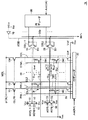
図1を参照して、MRAMデバイスは、外部からの制御信号(図示せず)およびアドレス信号Addに応じてランダムアクセスを実行し、書込データDinの入力および読出データDoutの出力を実行する。データ読出動作およびデータ書込動作に代表されるMRAMデバイス1の内部動作は、上記制御信号に応答して,図示しない制御回路によって発行される。当該内部動作は、たとえば外部からのクロック信号(図示せず)に同期したタイミングで実行される。あるいは、外部からクロック信号を受けることなく、MRAM内部で動作タイミングを定めてもよい。
Referring to FIG. 1, the MRAM device executes random access in response to an external control signal (not shown) and address signal Add, and executes input of write data Din and output of read data Dout. The internal operation of the
MRAMデバイス1aは、メモリセルアレイ10と、行デコーダ20と、列デコーダ30と、書込バッファ70と、データ読出アンプ80と、データバスDBおよび参照データバスDBrとを備える。
The MRAM device 1a includes a
メモリセルアレイ10には、行列状に配列された複数のMTJメモリセルMC(以下、単に「メモリセル」とも称する)と、ダミー行を形成するように配置されたデータ読出参照用の複数のダミーメモリセルDMCとが配置されている。
The
メモリセルの行(メモリセル行)に対応して、データ読出用のリードワード線RWLおよびデータ書込用のディジット線DLが配置される。一方、ダミーメモリセルの行(ダミーセル行)に対応して、データ読出用のダミーリードワード線DRWLが配置される。メモリセルMCおよびダミーメモリセルDMCはメモリセル列を共有するように配置され、メモリセル列にそれぞれ対応してビット線BLが配置される。 Corresponding to a row of memory cells (memory cell row), read word line RWL for data reading and digit line DL for data writing are arranged. On the other hand, a dummy read word line DRWL for data reading is arranged corresponding to a row of dummy memory cells (dummy cell row). Memory cell MC and dummy memory cell DMC are arranged to share a memory cell column, and bit line BL is arranged corresponding to each memory cell column.
各メモリセルMCおよび各ダミーメモリセルDMCは、ソース線SLによって所定電圧Vssと接続される。所定電圧Vssとしては接地電圧が一般的に用いられるので、以下においては所定電圧Vssを接地電圧Vssとも称する。 Each memory cell MC and each dummy memory cell DMC are connected to a predetermined voltage Vss by a source line SL. Since the ground voltage is generally used as the predetermined voltage Vss, hereinafter, the predetermined voltage Vss is also referred to as the ground voltage Vss.
各メモリセルMCは、対応のビット線BLおよびソース線SLの間に直列に接続されたアクセストランジスタATRおよびトンネル磁気抵抗素子TMRを有する。 Each memory cell MC has an access transistor ATR and a tunnel magnetoresistive element TMR connected in series between the corresponding bit line BL and source line SL.
ここで、MTJメモリセルの構成およびデータ記憶原理を説明する。 Here, the configuration of the MTJ memory cell and the data storage principle will be described.
図2は、MTJメモリセルの構成およびデータ記憶原理を説明する概念図である。 FIG. 2 is a conceptual diagram illustrating the configuration of the MTJ memory cell and the data storage principle.
図2を参照して、トンネル磁気抵抗素子TMRは、固定された一定の磁化方向を有する強磁性体層(以下、単に「固定磁化層」とも称する)FLと、外部からの印加磁界に応じた方向に磁化可能な強磁性体層(以下、単に「自由磁化層」とも称する)VLとを有する。固定磁化層FLおよび自由磁化層VLの間には、絶縁体膜で形成されるトンネルバリア(トンネル膜)TBが設けられる。自由磁化層VLは、書込データに応じて、固定磁化層FLと同一方向または固定磁化層FLと反対方向に磁化される。これらの固定磁化層FL、トンネルバリアTBおよび自由磁化層VLによって磁気トンネル接合(MTJ)が形成される。 Referring to FIG. 2, tunneling magneto-resistance element TMR corresponds to a ferromagnetic layer (hereinafter, also simply referred to as “fixed magnetization layer”) FL having a fixed fixed magnetization direction and a magnetic field applied from the outside. And a ferromagnetic layer (hereinafter, also simply referred to as “free magnetic layer”) VL that can be magnetized in the direction. A tunnel barrier (tunnel film) TB formed of an insulator film is provided between the fixed magnetic layer FL and the free magnetic layer VL. Free magnetic layer VL is magnetized in the same direction as fixed magnetic layer FL or in the opposite direction to fixed magnetic layer FL according to write data. These fixed magnetic layer FL, tunnel barrier TB and free magnetic layer VL form a magnetic tunnel junction (MTJ).
トンネル磁気抵抗素子TMRの抵抗は、固定磁化層FLおよび自由磁化層VLのそれぞれの磁化方向の相対関係に応じて変化する。具体的には、トンネル磁気抵抗素子TMRの抵抗は、固定磁化層FLの磁化方向と自由磁化層VLの磁化方向とが同じ(平行)である場合に最小値Rminとなり、両者の磁化方向が反対(反平行)方向である場合に最大値Rmaxとなる。 Resistance of tunneling magneto-resistance element TMR changes according to the relative relationship between the magnetization directions of fixed magnetic layer FL and free magnetic layer VL. Specifically, the resistance of the tunnel magnetoresistive element TMR becomes the minimum value Rmin when the magnetization direction of the fixed magnetization layer FL and the magnetization direction of the free magnetization layer VL are the same (parallel), and the magnetization directions of both are opposite. When the direction is (anti-parallel), the maximum value Rmax is obtained.
データ書込時においては、リードワード線RWLが非活性化されて、アクセストランジスタATRはターンオフされる。この状態で、自由磁化層VLを磁化するためのデータ書込磁界H(BL)およびH(DL)が、ビット線BLおよびディジット線DLを流れるデータ書込電流によってそれぞれ発生される。特に、ビット線BL上のデータ書込電流は、書込データのレベルに応じて、互いに反対方向のIw(0)およびIw(1)の一方に設定されるので、自由磁化層VLに印加されるデータ書込磁界H(BL)の方向は、書込データのレベルに応じて異なる。 At the time of data writing, read word line RWL is inactivated and access transistor ATR is turned off. In this state, data write magnetic fields H (BL) and H (DL) for magnetizing free magnetic layer VL are generated by data write currents flowing through bit line BL and digit line DL, respectively. In particular, the data write current on the bit line BL is set to one of Iw (0) and Iw (1) in opposite directions according to the level of the write data, so that it is applied to the free magnetic layer VL. The direction of the data write magnetic field H (BL) varies depending on the level of the write data.
図3は、MTJメモリセルのデータ書込電流と、トンネル磁気抵抗素子の磁化方向との関係を示す概念図である。 FIG. 3 is a conceptual diagram showing the relationship between the data write current of the MTJ memory cell and the magnetization direction of the tunnel magnetoresistive element.
図3を参照して、横軸H(EA)は、トンネル磁気抵抗素子TMR内の自由磁化層VLにおいて磁化容易軸(EA:Easy Axis)方向に印加される磁界を示す。一方、縦軸H(HA)は、自由磁化層VLにおいて磁化困難軸(HA:Hard Axis)方向に作用する磁界を示す。磁界H(EA)およびH(HA)は、図2に示したデータ書込磁界H(BL)およびH(DL)にそれぞれ対応する。 Referring to FIG. 3, the horizontal axis H (EA) indicates a magnetic field applied in the easy axis (EA) direction in free magnetic layer VL in tunneling magneto-resistance element TMR. On the other hand, the vertical axis H (HA) indicates a magnetic field that acts in the hard magnetization axis (HA) direction in the free magnetic layer VL. Magnetic fields H (EA) and H (HA) correspond to data write magnetic fields H (BL) and H (DL) shown in FIG. 2, respectively.
MTJメモリセルにおいては、固定磁化層FLの固定された磁化方向は、自由磁化層VLの磁化容易軸に沿っており、自由磁化層VLは、書込データに応じて、磁化容易軸方向に沿って、固定磁化層FLと平行あるいは反平行(反対)方向に磁化される。MTJメモリセルは、自由磁化層VLの2通りの磁化方向と対応させて、1ビットのデータを記憶することができる。 In the MTJ memory cell, the fixed magnetization direction of the fixed magnetic layer FL is along the easy axis of the free magnetic layer VL, and the free magnetic layer VL is along the easy axis direction according to the write data. Thus, it is magnetized in a direction parallel or antiparallel (opposite) to the fixed magnetization layer FL. The MTJ memory cell can store 1-bit data corresponding to the two magnetization directions of the free magnetic layer VL.
自由磁化層VLの磁化方向は、印加される磁界H(EA)およびH(HA)の和が、アステロイド特性線の外側の領域に達する場合にのみ新たに書換えることができる。すなわち、印加されたデータ書込磁界がアステロイド特性線の内側の領域に相当する強度である場合には、自由磁化層VLの磁化方向は変化しない。 The magnetization direction of the free magnetic layer VL can be newly rewritten only when the sum of the applied magnetic fields H (EA) and H (HA) reaches a region outside the asteroid characteristic line. That is, when the applied data write magnetic field has a strength corresponding to the region inside the asteroid characteristic line, the magnetization direction of the free magnetic layer VL does not change.
アステロイド特性線に示されるように、自由磁化層VLに対して磁化困難軸方向の磁界を印加することによって、磁化容易軸に沿った磁化方向を変化させるのに必要な磁化しきい値を下げることができる。図3に示すように、データ書込時の動作点は、ディジット線DLおよびビット線BLの両方に所定のデータ書込電流を流したときに、MTJメモリセルの記憶データ、すなわちトンネル磁気抵抗素子TMRの磁化方向を書換えられるように設計される。 As indicated by the asteroid characteristic line, by applying a magnetic field in the hard axis direction to the free magnetic layer VL, the magnetization threshold required to change the magnetization direction along the easy axis is lowered. be able to. As shown in FIG. 3, the operating point at the time of data writing is that the data stored in the MTJ memory cell, that is, the tunnel magnetoresistive element when a predetermined data write current is passed through both the digit line DL and the bit line BL. It is designed so that the magnetization direction of TMR can be rewritten.
図3に例示された動作点5a〜5dでは、データ書込対象であるMTJメモリセルにおいて、磁化容易軸方向のデータ書込磁界H(EA)の強度がHWRとなるように設計される。すなわち、このデータ書込磁界HWRが得られるように、ビット線BLまたはディジット線DLを流れるデータ書込電流の値が設計される。一般的に、データ書込磁界HWRは、磁化方向の切換えに必要なスイッチング磁界HSWと、マージン分ΔHとの和で示される。すなわち、HWR=HSW+ΔHで示される。 The operating points 5a to 5d illustrated in FIG. 3 are designed such that the strength of the data write magnetic field H (EA) in the easy axis direction is H WR in the MTJ memory cell that is the data write target. That is, the value of the data write current flowing through the bit line BL or the digit line DL is designed so that this data write magnetic field HWR is obtained. Generally, data write magnetic field H WR is the switching magnetic field H SW necessary for switching the magnetization direction is indicated by the sum of the margin [Delta] H. That is, H WR = H SW + ΔH.
また、磁化困難軸方向のデータ書込磁界H(HA)の方向は、MTJメモリセルの書込データへ影響を与えない。すなわち、動作点5a,5cのいずれによっても、同じ値のデータをMTJメモリセルに書込み可能であり、同様に、動作点5b,5dのいずれを用いても、同じ値のデータをMTJメモリセルに書込むことができる。
Further, the direction of the data write magnetic field H (HA) in the hard axis direction does not affect the write data of the MTJ memory cell. That is, the same value data can be written into the MTJ memory cell at any of the
トンネル磁気抵抗素子TMRに一旦書込まれた磁化方向、すなわちMTJメモリセルの記憶データは、新たなデータ書込が実行されるまでの間不揮発的に保持される。各メモリセルの抵抗は、厳密には、トンネル磁気抵抗素子TMR、アクセストランジスタATRのオン抵抗、およびその他の寄生抵抗の和であるが、トンネル磁気抵抗素子TMR以外の抵抗分は記憶データによらず一定であるので、以下においては、MTJメモリセルの記憶データに応じた2種類の抵抗についてもRmaxおよびRminで示し、両者の差をΔR(すなわち、ΔR=Rmax−Rmin)と示すものとする。 The magnetization direction once written in tunneling magneto-resistance element TMR, that is, data stored in the MTJ memory cell is held in a nonvolatile manner until new data writing is executed. Strictly speaking, the resistance of each memory cell is the sum of the tunnel magnetoresistive element TMR, the ON resistance of the access transistor ATR, and other parasitic resistances, but the resistance other than the tunnel magnetoresistive element TMR does not depend on the stored data. Therefore, in the following description, two types of resistances corresponding to the storage data of the MTJ memory cell are also indicated by Rmax and Rmin, and the difference between them is indicated by ΔR (that is, ΔR = Rmax−Rmin).
データ読出時には、アクセストランジスタATRをターンオンさせることによって生じるトンネル磁気抵抗素子TMRの通過電流を、ビット線BLを介して検知することにより、選択メモリセルの抵抗レベル、すなわち記憶データを読出可能である。 At the time of data reading, the resistance level of the selected memory cell, that is, the stored data can be read by detecting the passing current of tunneling magneto-resistance element TMR generated by turning on access transistor ATR through bit line BL.
再び図1を参照して、ダミーメモリセルDMCは、上述したメモリセルMCの2種類の抵抗RmaxおよびRminの中間抵抗Rref(たとえば、Rref=Rmin+ΔR/2)を有するように構成される。各ダミーメモリセルDMCは、ダミーリードワード線DRWLの活性化に応答して、参照データバスDBrおよびソース線SL(接地電圧Vss)の間に、中間抵抗Rrefを電気的に接続可能なように構成される。 Referring again to FIG. 1, dummy memory cell DMC is configured to have an intermediate resistance Rref (for example, Rref = Rmin + ΔR / 2) of two types of resistances Rmax and Rmin of memory cell MC described above. Each dummy memory cell DMC is configured so that an intermediate resistor Rref can be electrically connected between reference data bus DBr and source line SL (ground voltage Vss) in response to activation of dummy read word line DRWL. Is done.
なお、ダミーメモリセルDMCの構成は特に限定されないため、抵抗Rrefを製造時に固定することで、製造後におけるダミーメモリセルDMCへの磁気的なデータ書込を不要とする構成を採用することもできる。このような構成では、データ書込用のダミーディジット線DDLの配置は必要ない。しかしながら、製造時にメモリセルアレイ10の端部で形状が不連続となることによって寸法精度に支障をきたすことを防止するために、不使用の場合でもあえてダミーディジット線DDLを設ける構成としてもよい。
Since the configuration of the dummy memory cell DMC is not particularly limited, it is possible to employ a configuration in which magnetic data writing to the dummy memory cell DMC after manufacturing is not required by fixing the resistor Rref at the time of manufacturing. . In such a configuration, the arrangement of the dummy digit line DDL for data writing is not necessary. However, in order to prevent the dimensional accuracy from being hindered by the discontinuity of the shape at the end of the
各ディジット線DLの一端は、たとえばnMOSトランジスタが適用されたトランジスタスイッチ25を介して接地電圧Vssと接続される。一方、各ディジット線DLの他端側は、たとえばpMOSトランジスタが適用されたトランジスタスイッチ15を介して電源電圧Vccと接続される。各トランジスタスイッチ15は、ディジット線プリチャージ信号/DLPRの活性化に応答してターンオンする。一方、各トランジスタスイッチ25は、行デコーダ20による行アドレス信号Add(RA)のデコード結果に基づいて、データ書込時に選択行でターンオンされる。
One end of each digit line DL is connected to the ground voltage Vss through a
ダミーディジット線DDLは、トランジスタスイッチ15および25と同様に設けられたトランジスタスイッチ15♯および25♯によって、電源電圧Vccおよび接地電圧Vssと接続可能である。上述のように、ダミーメモリセルDMCへの磁気的なデータ書込が不要な構成においても、形状連続性確保のためにトランジスタスイッチ15♯および25♯をダミーとして設けてもよい。
Dummy digit line DDL can be connected to power supply voltage Vcc and ground voltage Vss by
各ビット線BLの一端側は、コラム選択スイッチ55を介してデータバスDBと接続される。一方、各ビット線BLの他端側には、ライトドライバ50が配置される。各ダミーメモリセルDMCは、コラム選択スイッチ55rを介して参照データバスDBrと接続される。
One end of each bit line BL is connected to the data bus DB via the
コラム選択スイッチ55,55rは、各メモリセル列に対応して設けられ、対応のコラム選択線CSLに応答してオン・オフされる。列デコーダ30は、コラムアドレス信号Add(CA)のデコード結果に基づいて、コラム選択スイッチ55,55rが選択列でオンし、非選択列でオフするように、各コラム選択線CSLの活性化を制御する。コラム選択スイッチ55,55rの各々には、たとえばnMOSトランジスタが適用される。
Column selection switches 55 and 55r are provided corresponding to each memory cell column, and are turned on / off in response to a corresponding column selection line CSL. The
図1においては、第1行および第2行ならびに第j列および第(j−1)列(j:自然数)に対応する、リードワード線RWL1,RWL2、ディジット線DL1,DL2、ビット線BLj−1,BLj、コラム選択線CSLj−1、CSLjおよびソース線SLj−1,SLjが代表的に図示されている。 In FIG. 1, read word lines RWL1 and RWL2, digit lines DL1 and DL2, bit lines BLj− corresponding to the first and second rows, the jth column and the (j−1) th column (j: natural number). 1, BLj, column selection lines CSLj-1, CSLj, and source lines SLj-1, SLj are representatively shown.
なお、本実施の形態においては、リードワード線、ディジット線、ビット線、コラム選択線およびソース線を総括的に表現する場合には符号RWL、DL、BL、CSLおよびSLをそれぞれ用いて表記することとする。また、データ、信号および信号線の高電圧状態(電源電圧Vcc)および低電圧状態(接地電圧Vss)のそれぞれを、「Hレベル」および「Lレベル」ともそれぞれ称することとする。 In this embodiment, when the read word line, digit line, bit line, column selection line, and source line are expressed collectively, they are expressed using the symbols RWL, DL, BL, CSL, and SL, respectively. I will do it. The high voltage state (power supply voltage Vcc) and low voltage state (ground voltage Vss) of the data, signal, and signal line are also referred to as “H level” and “L level”, respectively.
書込バッファ70は、データ端子71に入力された書込データDinに応答したデータ電圧をデータバスDBに駆動する。本実施の形態においては、書込データDin=HレベルのときにはデータバスDBが電源電圧(Vcc)に設定され、Din=Lレベルのときには、データバスDBは接地電圧(Vss)に設定されるものとする。すなわちデータ書込時において、電源電圧Vccおよび接地電圧Vssのそれぞれが「データ電圧」に相当する。
Write
ライトドライバ50は、上記データ電圧に相当する電源電圧Vccおよび接地電圧Vssと、対応のビット線BLとの間にそれぞれ電気的に接続されたトランジスタスイッチ51および52を有する。たとえば、トランジスタスイッチ51はpMOSトランジスタで構成され、トランジスタスイッチ52は、nMOSトランジスタで構成される。
Write
トランジスタスイッチ51のゲートには制御信号WDPが入力され、トランジスタスイッチ52のゲートには制御信号WDNが入力される。制御信号WDP,WDNは、各メモリセル列ごとに独立に生成される。図1には、第j列および第(j−1)列に対応する制御信号WDPj−1,WDPj,WDNj−1,WDNjが例示される。
A control signal WDP is input to the gate of the
データ読出アンプ80は、カレントミラーアンプを構成するnMOSトランジスタ81,82およびpMOSトランジスタ83,84と、当該カレントミラーアンプへ動作電流を供給するためのpMOSトランジスタ85とを有する。
The data read
nMOSトランジスタ81は、データバスDBおよびノードND1の間に電気的に接続され、nMOSトランジスタ82は参照データバスDBrおよびノードND2の間に電気的に接続される。pMOSトランジスタ83,84は、ノードND1およびND2とノードND3との間にそれぞれ電気的に接続される。pMOSトランジスタ85は、ノードND3および電源電圧Vccの間に電気的に接続され、ゲートにはセンスイネーブル信号/SEを受ける。
nMOSトランジスタ81および82のゲートには共通に所定電圧Vrefが与えられ、pMOSトランジスタ83および84のゲートは共通にノードND1と接続される。ノードND1には読出データDoutが生成され、ノードND2には読出データDoutの反転データ/Doutが出力される。
A predetermined voltage Vref is commonly applied to the gates of
次に、図1に示したMRAMデバイス1aのデータ書込動作およびデータ読出動作の概略について説明する。 Next, an outline of the data write operation and data read operation of the MRAM device 1a shown in FIG. 1 will be described.
データ書込動作時に、行デコーダ20によるトランジスタスイッチ25のオン・オフ制御により、選択行のディジット線DLには、書込データDinによらない所定方向のデータ書込電流Ipが流される一方で、非選択行のディジット線DLにはデータ書込電流Ipは流れない。データ書込電流Ipによって、図3に示した磁化困難軸方向に沿ったデータ書込磁界H(HA)が発生される。すなわち、データ書込電流Ipは本発明における「第1のデータ書込電流」に相当し、各ディジット線DLは本発明における「第1の書込電流線」に相当する。
During the data write operation, a data write current Ip in a predetermined direction that does not depend on the write data Din flows through the digit line DL of the selected row by the on / off control of the
さらに、ライトドライバ50を構成するトランジスタスイッチ51,52およびコラム選択スイッチ55のオン・オフ制御によって、選択列のビット線BLには、書込データDinに応じてデータ書込電流Iw(0)またはIw(1)のいずれかが流される。データ書込電流Iw(0)およびIw(1)は、図3で説明した磁化容易軸に沿ったデータ書込磁界H(EA)に相当する。一方、非選択列のビット線BLは、基本的にフローティング状態とされる。すなわち、トランジスタスイッチ51,52およびコラム選択スイッチ55はターンオフされる。
Further, by the on / off control of the transistor switches 51 and 52 and the
これにより、選択メモリセルに対しては、データ書込電流Ipと、データ書込電流Iw(0)またはIw(1)との両方によるデータ書込磁界が印加されて、図3に示した動作点5a〜5dのいずれかの状態が実現される。これにより、選択メモリセルのトンネル磁気抵抗素子TMRは、書込データDinに沿った方向に磁化される。すなわち、データ書込電流Iw(0),Iw(1)は本発明における「第2のデータ書込電流」に相当し、各ビット線BLは本発明における「第2の書込電流線」に相当する。
As a result, the data write magnetic field by both the data write current Ip and the data write current Iw (0) or Iw (1) is applied to the selected memory cell, and the operation shown in FIG. Any one of the
なお、後ほど詳細に説明するように、本発明に従うMRAMデバイスにおいては、電源電圧Vcc(代表的にはバッテリを想定)から見た、データ書込時におけるMRAMデバイスの消費電流、すなわち負荷電流波形が急峻とならないように制御される。 As will be described in detail later, in the MRAM device according to the present invention, the consumption current of the MRAM device at the time of data writing, that is, the load current waveform, as viewed from the power supply voltage Vcc (typically assumed to be a battery). It is controlled not to be steep.
データ読出時には、各ディジット線DL上に電流が流れないようにトランジスタスイッチ15,25を制御した上で、選択行のリードワード線RWLならびにダミーリードワード線DRWLが活性化される。これにより、選択メモリセルにおいてアクセストランジスタATRがオンし、選択列のビット線BLおよび接地電圧Vss(ソース線SL)の間にトンネル磁気抵抗素子TMRが接続される。さらに、選択列におけるコラム選択スイッチ55,55rのオンにより、データバスDBおよび接地電圧Vss(ソース線SL)の間には、選択メモリセルの記憶データに応じて抵抗RmaxおよびRminのいずれかが接続され、かつ、参照データバスDBrおよび接地電圧Vss(ソース線SL)の間には、ダミーメモリセルDMCの中間抵抗Rrefが接続される。 At the time of data reading, the transistor switches 15 and 25 are controlled so that no current flows on each digit line DL, and the read word line RWL and the dummy read word line DRWL of the selected row are activated. Thereby, access transistor ATR is turned on in the selected memory cell, and tunneling magneto-resistance element TMR is connected between bit line BL of the selected column and ground voltage Vss (source line SL). Further, when the column selection switches 55 and 55r in the selected column are turned on, either of the resistors Rmax and Rmin is connected between the data bus DB and the ground voltage Vss (source line SL) according to the storage data of the selected memory cell. In addition, an intermediate resistor Rref of the dummy memory cell DMC is connected between the reference data bus DBr and the ground voltage Vss (source line SL).
この状態で、Lレベルに活性化されたセンスイネーブル信号/SEに応答してpMOSトランジスタ85がターンオンすると、nMOSトランジスタ81,82およびpMOSトランジスタ83,84によって構成されるカレントミラーアンプに動作電流が供給される。これにより、nMOSトランジスタ81を介してノードND1と接続されるデータバスDBと、nMOSトランジスタ82を介してノードND2と接続される参照データバスDBrとの間には、選択メモリセルの記憶データに応じた極性の電流差が生じる。当該電流差は、上記カレントミラーアンプによってノードND1およびND2の間の電圧差に増幅される。これにより、選択メモリセルの記憶データに応じた読出データDoutがノードND1に生成される。
In this state, when the
次に、実施の形態に従うMRAMデバイス1aにおけるデータ書込電流の供給について詳細に説明する。 Next, supply of data write current in MRAM device 1a according to the embodiment will be described in detail.
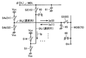
図4は、この発明の実施の形態1に従うデータ書込電流供給構成を説明する概念図である。 FIG. 4 is a conceptual diagram illustrating a data write current supply configuration according to the first embodiment of the present invention.
図4においては、選択行に対応するディジット線DLi(以下、「選択ディジット線」とも称する)および選択列に対応するビット線BLj(以下、「選択ビット線」とも称する)が代表的に示されている。 FIG. 4 representatively shows digit line DLi (hereinafter also referred to as “selected digit line”) corresponding to the selected row and bit line BLj (hereinafter also referred to as “selected bit line”) corresponding to the selected column. ing.
既に説明したように、選択ディジット線DLiの一端側は、「第1のスイッチ素子」に相当するスイッチ素子S1を介して接地電圧Vssと接続可能であり、かつ、その他端側は「第2のスイッチ素子」であるスイッチ素子S2を介して電源電圧Vccと接続されている。なお、スイッチ素子S1は図1に示したトランジスタスイッチ25に相当し、スイッチ素子S2は図1に示されたトランジスタスイッチ15に相当する。
As described above, one end side of the selected digit line DLi can be connected to the ground voltage Vss via the switch element S1 corresponding to the “first switch element”, and the other end side can be connected to the “second switch”. It is connected to the power supply voltage Vcc via a switch element S2 which is a “switch element”. The switch elements S1 corresponds to
符号60は、ディジット線DLの充電容量を示す。ディジット線容量60は、ディジット線DLの寄生容量62aのみで構成されてもよいし、ディジット線DLと接続された容量素子(付加容量)62bと寄生容量62aとの和で構成されてもよい。
選択ビット線BLjの一端側は、「第3のスイッチ素子」であるスイッチ素子S3を介して、書込データDinに応じたデータ電圧に設定される書込ノード75と接続される。スイッチ素子S3は、図1に示したコラム選択スイッチ55に相当し、書込ノード75は、図1におけるデータ端子71またはデータバスDBに相当する。すなわち、書込ノード75に設定されるデータ電圧は、電源電圧Vcc(Din=Hレベル)および接地電圧Vss(Din=Lレベル)のいずれかである。
One end of the selected bit line BLj is connected to a
ビット線BLjの他端は、「第4のスイッチ素子」に相当するスイッチ素子S4a,S4bを介して、「データ電圧」に相当する電源電圧Vccおよび接地電圧Vssとそれぞれ電気的に接続可能である。スイッチ素子S4aは図1に示したトランジスタスイッチ51に相当し、スイッチ素子S4bは、図1に示したトランジスタスイッチ52に相当する。
The other end of the bit line BLj can be electrically connected to the power supply voltage Vcc and the ground voltage Vss corresponding to the “data voltage” via the switch elements S4a and S4b corresponding to the “fourth switch element”. . The switch element S4a corresponds to the
符号65は、ビット線BLの充電容量を示す。ビット線容量65は、ビット線BLの寄生容量67aのみで構成されてもよいし、ビット線BLと接続された容量素子(付加容量)67bと寄生容量67aとの和で構成されてもよい。
図5には、付加容量62b,67bの好ましい配置が示される。
FIG. 5 shows a preferred arrangement of the
図5を参照して、メモリセルアレイ10には、m行×n列(m,n:自然数)にメモリセルMCが配置され、メモリセル行に対応してディジット線DL1〜DLmが配置され、メモリセル列に対応してビット線BL1〜BLnが配置される。
Referring to FIG. 5, in
充電経路の上流側のメモリセルMCでは、当該充電経路の下流側のメモリセルMCと比較してデータ書込電流供給のための電荷蓄積に利用できる寄生容量62a,62bが小さい。なお、各ディジット線DL上においては、スイッチ素子S2側が充電経路の上流側に相当し、スイッチ素子S1側が充電経路の下流側に相当する。同様に、各ビット線BL上においては、スイッチ素子S3側が充電経路の上流側に相当し、ライトドライバ50側が充電経路の下流側に相当する。
In the memory cell MC on the upstream side of the charging path, the
したがって、寄生容量62a,67aによる充電容量の不足を補助するための付加容量62b,67bは、各ディジット線DLおよび各ビット線BLの充電経路において、メモリセルMCよりも上流側に設ける必要がある。すなわち、付加容量62bは、メモリセルアレイ10外部のスイッチ素子S2側の領域で各ディジット線DLと接続されるように設けられる。同様に、付加容量67bは、メモリセルアレイ10外部のスイッチ素子S3側の領域で各ビット線BLと接続されるように設けられる。
Therefore, the
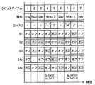
図6は、実施の形態1に従うMRAMデバイスの動作を説明する図である。 FIG. 6 is a diagram for explaining the operation of the MRAM device according to the first embodiment.
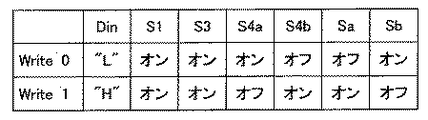
図6を参照して、実施の形態1に従うMRAMデバイス1aの動作は、クロック信号に応答してクロックサイクルごとに実行されるものとする。 Referring to FIG. 6, it is assumed that operation of MRAM device 1a according to the first embodiment is executed every clock cycle in response to a clock signal.
クロックサイクル1ではスタンバイ動作(Stby)が実行され、データ読出およびデータ書込のいずれも実行されない。スタンバイ動作では、スイッチ素子S2およびS4bがオンされ、スイッチ素子S1,S3,S4aはオフされる。これにより各ディジット線DLが電源電圧Vccによって充電されるが、スイッチ素子S1がオフされているためデータ書込電流は生じない。同様に、各ビット線BLは接地電圧Vssにプリチャージされる。
In
クロックサイクル2ではデータ読出動作(Read)が実行される。各ディジット線DLはデータ読出動作には無関係であるため、スイッチS1およびS2がスタンバイ動作時と同様に制御され、各ディジット線DLの充電状態が保持される。
In
図1で説明したように、データ読出は、選択ビット線に選択メモリセルが接続されて実行される。スイッチ素子S3は、データ書込動作に関連してはオフされるべきであるが、図1に示した構成例ではビット線BLをデータ読出およびデータ書込で共用しているため、選択列においてオンする必要がある。したがって、図6では、スイッチ素子S3の状態を括弧付きの“オン”で示している。一方、ライトドライバ内のスイッチ素子S4a,S4bはデータ読出動作に支障を来たさないようにオフされる。 As described with reference to FIG. 1, data reading is performed with the selected memory cell connected to the selected bit line. Switch element S3 should be turned off in connection with the data write operation, but in the configuration example shown in FIG. 1, since bit line BL is shared for data reading and data writing, in the selected column Need to turn on. Therefore, in FIG. 6, the state of the switch element S3 is indicated by “ON” with parentheses. On the other hand, the switch elements S4a and S4b in the write driver are turned off so as not to interfere with the data read operation.
クロックサイクル3においては、次のサイクルからデータ書込を実行するために、再びスタンバイ動作が実行される。
In
クロックサイクル4〜8は単一のデータ書込動作を構成する。単一のデータ書込動作では、データ“0”(Din=Lレベル)を書込む“Write0”およびデータ“1”(Din=Hレベル)を書込む“Write1”のいずれかが実行される。図6に示す例では、クロックサイクル4〜8により“Write0”が実行されるものとする。
Clock cycles 4-8 constitute a single data write operation. In a single data write operation, either “Write0” for writing data “0” (Din = L level) or “Write1” for writing data “1” (Din = H level) is executed. In the example illustrated in FIG. 6, “Write0” is executed in
先頭のクロックサイクル4において、書込ノード75は、書込データに応じたデータ電圧(“Write0”では接地電圧Vss)に設定される。
In the
クロックサイクル4では、スイッチ素子S3がターンオンされる一方で、スイッチ素子S1,S2,S4a,S4bはオフされる。
In
スイッチ素子S3がターンオンし、かつ、スイッチ素子S4a,S4bがオフされるので、選択ビット線BLjはデータ“0”(Din=Lレベル)に対応したデータ電圧レベル(接地電圧Vss)に充電される。 Since the switch element S3 is turned on and the switch elements S4a and S4b are turned off, the selected bit line BLj is charged to the data voltage level (ground voltage Vss) corresponding to the data “0” (Din = L level). .
また、選択ディジット線DLiは、電源電圧Vccへの充電状態が維持され、データ書込電流Ipはこの段階では流されない。このように、クロックサイクル4において、ディジット線容量60は電源電圧Vccで充電され、ビット線容量65は、書込データDinに応じて接地電圧Vssに充電される。
Further, the selected digit line DLi is kept charged to the power supply voltage Vcc, and the data write current Ip is not passed at this stage. Thus, in
次のクロックサイクル5では、スイッチ素子S3がターンオフされる一方で、スイッチ素子S1およびS4aはターンオンする。一方、スイッチ素子S2およびS4bはオフ状
態を維持する。
In the
これにより、電源電圧Vccに充電された状態の選択ディジット線DLiが接地電圧Vssに接続されることによって、選択ディジット線DLi上を所定方向(ここでは、スイッチ素子S2からS1への方向)にデータ書込電流Ipが流れる。データ書込電流Ipは、クロックサイクル4迄に充電されたディジット線容量60の放電電流に相当し、放電が完了すると消滅する。
As a result, the selected digit line DLi charged to the power supply voltage Vcc is connected to the ground voltage Vss, whereby the data on the selected digit line DLi is transmitted in a predetermined direction (here, the direction from the switch element S2 to S1). A write current Ip flows. Data write current Ip corresponds to the discharge current of
さらに、スイッチ素子S4aのターンオンによって、書込データDinに対応するデータ電圧(ここでは接地電圧Vss)に充電された状態の選択ビット線BLjは、異なるデータ電圧である電源電圧Vccと接続される。これにより、書込データDinに応じた方向のデータ書込電流Iw(0)が選択ビット線BLj上を流れる。データ書込電流Iw(0)は、ビット線容量65の電源電圧Vccへの充電電流に相当し、充電が完了すると消滅する。この結果、選択メモリセルへデータ“0”が書込まれる。
Further, when the switch element S4a is turned on, the selected bit line BLj charged to the data voltage (here, the ground voltage Vss) corresponding to the write data Din is connected to the power supply voltage Vcc which is a different data voltage. As a result, the data write current Iw (0) in the direction corresponding to the write data Din flows on the selected bit line BLj. Data write current Iw (0) corresponds to a charging current to power supply voltage Vcc of
続くクロックサイクル6では、書込ノード75は、再び、書込データに応じたデータ電圧(“Write0”では接地電圧Vss)に設定される。
In
さらに、クロックサイクル4と同様に、スイッチ素子S3がターンオンされて、スイッチ素子S1,S2,S4a,S4bがターンオフされる。これにより、選択ビット線BLjは、クロックサイクル4と同様に、書込データに応じたデータ電圧(接地電圧Vss)に再び充電される。一方、スイッチ素子S1,S2がオフされるため、選択ディジット線DLiの状態は、クロックサイクル5の終了時と同様に維持される。
Further, similarly to the
続くクロックサイクル7では、スイッチ素子S2がターンオンされる。これにより、クロックサイクル4と同様に、ディジット線容量60が電源電圧Vccに充電されるが、スイッチ素子S1がオフされているので、データ書込電流Ipは流れない。また、スイッチ素子S3,S4a,S4bがオフされるため、選択ビット線BLjの状態は、クロックサイクル6の終了時と同様に維持される。
In the
クロックサイクル8においては、スイッチ素子S1およびS4bがターンオンされる一方で、スイッチ素子S2,S3,S4aがオフされる。しかし、選択ビット線BLjはクロックサイクル7において接地電圧Vssに充電されているので、データ書込電流が流れることはない。したがって、このクロックサイクルにおいては、選択ディジット線DLj上をデータ書込電流Ipが流れるものの、選択ビット線BLj上をデータ書込電流が流れないため、データ書込は実行されない。
In
このようにして、クロックサイクル4〜8で構成される単一のデータ書込動作によって、クロックサイクル5でのデータ書込電流供給により、データ“0”(Din=Lレベル)のデータ書込が実行される。
In this way, data “0” (Din = L level) is written by supplying a data write current in
クロックサイクル9においては、クロックサイクル1および3と同様のスタンバイ動作が実行される。すなわち、各ディジット線DLは電源電圧Vccに充電され、各ビット線BLは接地電圧Vssに充電される。
In
なお、“Write1”のデータ書込動作は、クロックサイクル4および6での書込ノード75の電圧設定を、Din=Hレベルに対応したデータ電圧(電源電圧Vcc)に変更した上で、スイッチ素子S1〜S3,S4a,S4bを“Write0”と同様にスイッチングさせることにより実行される。これにより、“Write1”では、クロックサイクル5では選択ビット線BLjにデータ書込電流が発生しない一方で、クロックサイクル8で選択ビット線BLjにデータ書込電流Iw(1)が流れることにより、選択メモリセルへデータ“1”が書込まれる。
Note that the data write operation of “Write1” is performed by changing the voltage setting of the
すなわち、図6に示す書込動作シーケンスでは、5つのクロックサイクルで構成される単一の書込動作において、書込データによらずスイッチ素子S1〜S3,S4a,S4bのスイッチングパターンを同一とできる。このため、書込データに応じてスイッチ素子S4aおよびS4bの動作を制御する必要がないので、そのオン・オフを制御する回路、すなわち図1に示した制御信号WDP,WDNを生成する制御回路の構成を簡素化できる。 That is, in the write operation sequence shown in FIG. 6, the switching patterns of the switch elements S1 to S3, S4a, and S4b can be made the same regardless of the write data in a single write operation composed of five clock cycles. . For this reason, it is not necessary to control the operation of the switch elements S4a and S4b in accordance with the write data, so that the circuit for controlling the on / off, that is, the control circuit for generating the control signals WDP and WDN shown in FIG. The configuration can be simplified.
このように本発明に従うMRAMデバイスにおけるデータ書込電流は、「書込電流線」として設けられたディジット線およびビット線の容量の充放電動作によって供給される。以下では、これらの充放電電流の特性について、ディジット線DLiを例にとって説明する。 As described above, the data write current in the MRAM device according to the present invention is supplied by the charge / discharge operation of the capacitance of the digit line and the bit line provided as the “write current line”. Hereinafter, the characteristics of these charge / discharge currents will be described using the digit line DLi as an example.
図7は、データ書込電流供給に関連するディジット線の充放電動作をモデル化した第1の電気回路図である。 FIG. 7 is a first electric circuit diagram modeling the charge / discharge operation of the digit line related to the data write current supply.
図7を参照して、ディジット線DLiは、スタンバイ動作時等(図6のクロックサイクル1,3,7,9)において、スイッチ素子S2のターンオンに応答して、電源電圧Vccと接続される。すなわち、ディジット線容量60が電源電圧Vccによって充電される。この充電動作は一般的なRC負荷の充電動作に相当するため、充電経路の充電抵抗をR0とすると、充電電流ic(t)およびディジット線電圧vc(t)は、下記(1)式および(2)式で示される。なお、充電抵抗R0には、充電経路の寄生抵抗およびトランジスタスイッチ15のオン抵抗等が含まれる。
Referring to FIG. 7, digit line DLi is connected to power supply voltage Vcc in response to turn-on of switch element S2 during a standby operation or the like (clock cycles 1, 3, 7, 9 in FIG. 6). That is, the

次に、スイッチ素子S2がターンオフされた状態でスイッチ素子S1をターンオンすることにより(たとえば図6でのクロックサイクル5,8)、ディジット線容量60の充電電荷が接地電圧Vssへ放電されることで、データ書込電流Ipが流される。放電経路の放電抵抗をRpとすると、放電電流id(t)およびディジット線電圧vc(t)は下記(3),(4)式のように示される。なお、放電抵抗Rpには、放電経路の寄生抵抗およびトランジスタスイッチ25のオン抵抗等が含まれる。
Next, by turning on the switch element S1 in a state where the switch element S2 is turned off (for example, clock cycles 5 and 8 in FIG. 6), the charge of the
なお、(1)〜(4)式では、接地電圧Vss=0Vとし、Vcc−Vss=Vccとしている。(1)〜(4)式を概略的に図示すると、図8(a),(b)のようになる。 In the equations (1) to (4), the ground voltage Vss = 0V and Vcc−Vss = Vcc. When the equations (1) to (4) are schematically illustrated, they are as shown in FIGS.
図8(a)を参照して、充電時には、ディジット線容量60の充電電流ic(t)は、充電抵抗R0に依存したVcc/R0をピーク値とする減衰電流となる。充電電流ic(t)の減衰レートはディジット線容量60および充電抵抗R0の積の逆数である、“1/(C・R0)”に依存する。
Referring to FIG. 8 (a), at the time of charging, the charging current ic digit line capacitance 60 (t) is a damping current to a peak value of Vcc / R0 dependent on charging resistor R0. The decay rate of the charging current ic (t) depends on “1 / (C · R0)”, which is the reciprocal of the product of the
一方放電時には、図8(b)に示されるように、データ書込電流Ipに相当する放電電流id(t)は、放電抵抗Rpに依存するVcc/Rpをピーク値とする減衰電流となる。放電電流id(t)の減衰レートは、ディジット線容量60および放電抵抗RpのRC積の逆数である、1/(C・Rp)に依存する。
On the other hand, at the time of discharge, as shown in FIG. 8B, the discharge current id (t) corresponding to the data write current Ip becomes an attenuation current having a peak value of Vcc / Rp depending on the discharge resistance Rp. The decay rate of the discharge current id (t) depends on 1 / (C · Rp), which is the reciprocal of the RC product of the
したがって、データ書込に必要なデータ書込電流レベルをIwmとし、必要な電流印加時間をTwmとすると、放電電流id(t)>Iwmである期間Twが、Tw>Twmとなるように、放電抵抗RpおよびRC積C・Rpを設計する必要がある。 Therefore, when the data write current level necessary for data writing is Iwm and the necessary current application time is Twm, the discharge is performed so that the period Tw in which the discharge current id (t)> Iwm satisfies Tw> Twm. It is necessary to design the resistance Rp and the RC product C · Rp.
特に、ディジット線容量60の容量値Cについては、少なくとも、C・(Vcc−Vss)がIwmおよびTwmの積よりも大きくなるように、すなわち下記(5)式を満たすように設計する必要がある。
Particularly, the capacitance value C of the
一般的な数値例では、Twm=0.5〜2(ns),Iwm=3〜10(mA)程度であるので、Vcc=1.0(V)およびVss=0(V)とすると、ディジット線容量60としては、C=1.5〜20(pF)程度を確保する必要が生じる。ディジット線DLの寄生容量はその設計に依存して変化するので、図4に示した寄生容量62aのみで上記(5)式を満足する容量値が得られない場合には、容量素子62bを付加的に設けてディジット線DLに接続する必要がある。すなわち、図4に示されたディジット線容量60は、上記(5)式を満足するように、ディジット線DLの寄生容量62bのみ、もしくは寄生容量62aと付加容量62bとの和によって実現されることになる。
In a general numerical example, Twm = 0.5 to 2 (ns) and Iwm = 3 to 10 (mA), so when Vcc = 1.0 (V) and Vss = 0 (V), the digit As the
実施の形態1に従うMRAMデバイスでは、ディジット線容量60の充電動作と、データ書込電流のための放電動作とを異なる期間に実行するため、電源電圧Vccを供給する電源(バッテリ)からMRAMデバイスへの負荷電流は、図8(a)での充電電流ic(t)に相当する。すなわち、電源から見た負荷電流を比較的緩やかな波形とすることができる。
In the MRAM device according to the first embodiment, the charging operation for
一方、図7に示した構成において、スイッチ素子S1の配置を省略してスイッチ素子S2のみを設け、スイッチ素子S2を行選択結果に応じてオン・オフさせても、データ書込電流Ipの供給を実行できる。しかしながら、このような構成では、スイッチ素子S2のオン期間を通じて、定常的なデータ書込電流Ip=(Vcc−Vss)/(R0+Rp)が電源から供給され、さらに、当該オン期間の初期においてはディジット線容量60の充電電流がさらに重畳して供給される。したがって、電源から見た負荷電流は、図8(a)に示した充電電流ic(t)よりも短時間・大電流の波形となり、そのピーク値も高くなる。このため、バッテリ等の電源の負担が大きくなり、電力供給可能期間が短くなってしまう可能性がある。
On the other hand, in the configuration shown in FIG. 7, even if the switch element S1 is omitted and only the switch element S2 is provided and the switch element S2 is turned on / off according to the row selection result, the data write current Ip is supplied. Can be executed. However, in such a configuration, the steady data write current Ip = (Vcc−Vss) / (R0 + Rp) is supplied from the power source through the ON period of the switch element S2, and moreover, in the initial stage of the ON period, the digit is set. The charging current of the
言い換えれば、この発明の実施の形態1によるMRAMデバイスでは、電源から見た負荷電流を緩やかな波形に改善することによって、電源(バッテリ)の負荷を軽減できる。 In other words, in the MRAM device according to the first embodiment of the present invention, the load on the power source (battery) can be reduced by improving the load current viewed from the power source into a gentle waveform.
さらに、図9に示されるように、ディジット線容量60の充電経路に充電調整抵抗Rcを挿入することにより、充電経路のRC積を大きく確保することも可能である。なぜなら、スイッチ素子S2の配置により、データ書込電流Ipの供給期間には充電調整抵抗Rcをデータ書込電流経路から切り離す構成としているからである。なお、図9に示した充電調整抵抗Rcは、ディジット線DLに対しては、図1に示した電源電圧Vcc(バッテリに相当)とトランジスタスイッチ15との間に接続されるように配置すればよい。
Furthermore, as shown in FIG. 9, it is possible to secure a large RC product of the charging path by inserting the charging adjustment resistor Rc into the charging path of the
図9の構成における充電電流ic♯(t)は、下記(6)式で示される。 The charging current ic # (t) in the configuration of FIG. 9 is expressed by the following equation (6).
(2)式の充電電流ic(t)および(6)式の充電電流ic♯(t)の比較から理解されるように、充電調整抵抗Rcを追加することにより、電源から見た負荷電流のピーク値を抑制して、さらに緩やかな波形に改善することができる。したがって、充電時間は長期化するものの、高速動作が必要とされない用途に適用すれば電源の(バッテリ)負荷をさらに軽減できる。 As can be understood from the comparison of the charging current ic (t) in the equation (2) and the charging current ic # (t) in the equation (6), by adding the charging adjustment resistor Rc, the load current as viewed from the power source can be reduced. The peak value can be suppressed and the waveform can be further improved. Accordingly, although the charging time is prolonged, the (battery) load of the power source can be further reduced if applied to an application where high-speed operation is not required.
あるいは、図10に示すように、ディジット線容量60の容量値Cが十分に確保され、充電抵抗R0とのRC積R0・Cが十分大きい場合には、スイッチ素子S2の配置を省略する構成とすることもできる。この構成においては、充電電流ic(t)は図7の構成と同様に流れるが、スイッチ素子S1のターンオンに応答して流れる放電電流id♯(t)すなわちデータ書込電流Ipは下記(7)式のように示される。
Alternatively, as shown in FIG. 10, when the capacitance value C of the
スイッチ素子S1のオン期間においては、(7)式に示されるデータ書込電流id♯(t)のうち、ディジット線容量60の放電電荷によっては賄えない不足分の電流が電源(バッテリ)より供給されることとなる。したがって、図10に示した構成では、データ書込電流の供給期間(スイッチ素子S1のオン期間)における上記不足分の電流分だけ、電源(バッテリ)の負荷が増加するが、データ書込電流の供給期間前での充電電荷によって、データ書込電流の一部を供給する構成である点は変わらないため、電源(バッテリ)の負荷を軽減できる。
During the ON period of the switch element S1, a deficient current that cannot be covered by the discharge charge of the
なお、図7から図10では、ディジット線DL上のデータ書込電流供給動作について説明したが、ビット線BL上のデータ書込電流供給動作についても、その充電電流および放電電流は同様である。 7 to 10, the data write current supply operation on the digit line DL has been described. However, the charge current and the discharge current are the same in the data write current supply operation on the bit line BL.
すなわち、図11および図12に示すように、図7および図9の構成において、スイッチ素子S2をスイッチ素子S3(コラム選択スイッチ55)に置換し、スイッチ素子S1をスイッチ素子S4a,S4bに置換し、ディジット線容量60をビット線容量65に置換すれば、データ書込電流供給に関連するビット線の充放電動作をモデル化した電気回路図が実現される。
That is, as shown in FIGS. 11 and 12, in the configuration of FIGS. 7 and 9, switch element S2 is replaced with switch element S3 (column selection switch 55), and switch element S1 is replaced with switch elements S4a and S4b. If the
なお、ビット線BL上におけるデータ書込電流の供給動作時には、電源電圧Vccに充電されたビット線容量65を接地電圧Vssへ放電する動作(データ書込電流Iw(1)の供給に相当)のみでなく、ビット線容量65を接地電圧Vssに設定した後電源電圧Vccによって充電する動作(データ書込電流Iw(0)の供給に相当)が存在する。
In the operation of supplying the data write current on the bit line BL, only the operation of discharging the
しかしながら、このような動作においても、図8(a),(b)における電圧vc(t)の波形は極性が反転するものの、充電電流ic(t),ic♯(t)および放電電流id(t),id♯(t)については、上述したディジット線電流におけるデータ電流供給動作の場合と同様の波形となる。したがって、ビット線上のデータ書込電流供給についても、ディジット線上のデータ書込電流供給と同様に、電源(バッテリ)の負荷を軽減できる。 However, even in such an operation, although the polarity of the waveform of the voltage vc (t) in FIGS. 8A and 8B is reversed, the charging currents ic (t), ic # (t) and the discharging current id ( t) and id # (t) have waveforms similar to those in the data current supply operation in the digit line current described above. Therefore, the supply of the data write current on the bit line can also reduce the load on the power supply (battery), similar to the supply of the data write current on the digit line.
なお、ビット線BL上のデータ電流供給動作に関する充電調整抵抗Rcは、スイッチ素子S3と図1に示したデータ端子71との間に、スイッチ素子S3のオン期間にビット線BLと直列に接続される形態で配置することができる。
The charge adjustment resistor Rc related to the data current supply operation on the bit line BL is connected in series with the bit line BL during the ON period of the switch element S3 between the switch element S3 and the
また、充電抵抗R0は、書込バッファ70からビット線BLを含む充電経路の寄生抵抗およびスイッチ素子S3のオン抵抗の和に対応し、放電抵抗Rpは、ビット線BLの寄生抵抗およびスイッチ素子S4aまたはS4bのオン抵抗の和に相当する。
The charging resistor R0 corresponds to the sum of the parasitic resistance of the charging path including the bit line BL from the
以上説明したように、この発明の実施の形態1に従うMRAMデバイスにおいては、データ書込電流Ipおよび,Iw(0),Iw(1)を供給するための「書込配線」に相当するディジット線DLおよびビット線BLの容量充電動作と、データ書込電流の供給動作とを時分割で行ない、当該容量へ充電された電荷の放電によってデータ書込電流を供給する。これにより、電源電圧Vccを供給する電源(バッテリ)からMRAMデバイスへ供給される負荷電流の波形をなだらかなものとできるため、バッテリの負担を軽減できる。これにより、電源(バッテリ)からの電力供給可能期間を拡大して、MRAMデバイスの搭載機器の駆動可能時間を長期化できる。 As described above, in the MRAM device according to the first embodiment of the present invention, the digit line corresponding to “write wiring” for supplying data write current Ip and Iw (0), Iw (1) The capacity charging operation of the DL and the bit line BL and the operation of supplying the data write current are performed in a time-sharing manner, and the data write current is supplied by discharging the charge charged to the capacity. Thereby, since the waveform of the load current supplied from the power supply (battery) supplying the power supply voltage Vcc to the MRAM device can be made gentle, the burden on the battery can be reduced. As a result, the period in which power can be supplied from the power source (battery) can be extended, and the drivable time of the device on which the MRAM device is mounted can be extended.
特に、スイッチ素子S2を設けることによって、充電調整抵抗Rcをデータ書込電流のレベルに悪影響を与えることなく挿入可能となるので、充電時間の長期化によって要求される動作時間に支障を来さない用途においては、電源(バッテリ)による電力供給可能期間をさらに拡大することができる。 In particular, the provision of the switch element S2 allows the charge adjustment resistor Rc to be inserted without adversely affecting the level of the data write current, and therefore does not hinder the operation time required by extending the charge time. In applications, it is possible to further extend the period in which power can be supplied by the power source (battery).
[実施の形態1の変形例1]
実施の形態1の変形例1においては、実施の形態1によるMRAMデバイスにおける、データ書込動作シーケンスの他の構成例を説明する。
[
In the first modification of the first embodiment, another configuration example of the data write operation sequence in the MRAM device according to the first embodiment will be described.
図13は、実施の形態1の変形例1に従うMRAMデバイスの動作を説明する図である。 FIG. 13 is a diagram for explaining the operation of the MRAM device according to the first modification of the first embodiment.
図13を参照して、実施の形態1の変形例に従うデータ書込動作では、単一のデータ書込動作は、2つのクロックサイクルから構成される。単一のデータ書込動作では、データ“0”を書込む“Write0”およびデータ“1”を書込む“Write1”のいずれかが実行される。図13においては、クロックサイクル1〜3では、図6に示した動作シーケンスと同様に、スタンバイ動作(Stby)、読出動作(Read)およびスタンバイ動作(Stby)がそれぞれ実行される。
Referring to FIG. 13, in the data write operation according to the modification of the first embodiment, a single data write operation is composed of two clock cycles. In a single data write operation, either “Write0” for writing data “0” or “Write1” for writing data “1” is executed. In FIG. 13, in
クロックサイクル4および5によって、データ“0”を書込むための単一のデータ書込動作(Write0)が構成される。 Clock cycles 4 and 5 constitute a single data write operation (Write0) for writing data “0”.
先頭のクロックサイクル4においては、図6に示したクロックサイクル4と同様の動作が実行されて、選択ビット線BLjは、書込ノード75により書込データDinに応じて接地電圧Vssに充電される。また、クロックサイクル4では、選択ディジット線DLiは電源電圧Vccへの充電状態を維持される。
In the
次のクロックサイクル5において、スイッチ素子S1およびS2は、図6に示したクロックサイクル5と同様に制御される。
In the
これにより、選択ディジット線DLi上をデータ書込電流Ipが流れる。また、図6に示したクロックサイクル4と同様に、スイッチ素子S3もオフされるので、選択ビット線BLjは、ハイインピーダンス状態(Z)とされた書込ノード75から切離される。
Thereby, data write current Ip flows on selected digit line DLi. Similarly to
実施の形態1の変形例に従うデータ書込動作では、ライトドライバ50(図1)を構成するスイッチ素子S4aおよびS4bのオンおよびオフは、書込データDinに応じて制御される。クロックサイクル5では、Din=Lレベルに対応して、スイッチ素子S4aがオンされる一方で、スイッチ素子S4bがオフされる。これにより、書込データDinに応じて接地電圧Vssに充電された選択ビット線BLjがスイッチ素子S4aによって電源電圧Vccと接続されるので、選択ビット線BLj上を、データ書込電流Iw(0)が流れる。これにより、選択メモリセルへデータ“0”が書込まれる。
In the data write operation according to the modification of the first embodiment, on and off of switch elements S4a and S4b constituting write driver 50 (FIG. 1) are controlled in accordance with write data Din. In
クロックサイクル6におけるスタンバイ動作については、クロックサイクル1および3と同様である。
The standby operation in
クロックサイクル7および8によって、データ“1”を書込むための単一のデータ書込動作(Write1)が構成される。 Clock cycles 7 and 8 constitute a single data write operation (Write1) for writing data “1”.
クロックサイクル7においては、クロックサイクル4と同様の動作が実行されて、選択ディジット線DLiは電源電圧Vccに充電され、かつ、選択ビット線BLjは、書込ノード75により書込データDinに応じて電源電圧Vccに充電される。
In
次のクロックサイクル8では、図13のクロックサイクル4と同様に、選択ディジット線DLi上をデータ書込電流Ipが流れる。また、図6に示したクロックサイクル4と同様に、スイッチ素子S3もオフされるので、選択ビット線BLjはハイインピーダンス状態(Z)とされた書込ノード75から切離される。
In the
さらに、Din=Hレベルに対応して、スイッチ素子S4bがオンされる一方で、スイッチ素子S4aがオフされる。すなわち、書込データが異なるデータ書込動作間では、スイッチ素子S4a,S4bのオン・オフが入れ替わる。これにより、書込データDinに応じて電源電圧Vccに充電された選択ビット線BLjがスイッチ素子S4bによって接地電圧Vssと接続される。この結果、選択ビット線BLj上を、データ書込電流Iw(1)が流れて、クロックサイクル8で選択メモリセルへデータ“1”が書込まれる。
Further, in response to Din = H level, the switch element S4b is turned on while the switch element S4a is turned off. That is, the switching elements S4a and S4b are turned on / off between data write operations with different write data. As a result, the selected bit line BLj charged to the power supply voltage Vcc according to the write data Din is connected to the ground voltage Vss by the switch element S4b. As a result, data write current Iw (1) flows on selected bit line BLj, and data “1” is written to the selected memory cell in
次のクロックサイクル9におけるスタンバイ動作についても、クロックサイクル1、3および6と同様であるので説明は繰返さない。
Since the standby operation in the
このように、実施の形態1の変形例に従うデータ書込動作では、実施の形態1によるMRAMデバイスと同様の構成により、データ書込電流供給に関する電源(バッテリ)負荷を軽減するとともに、さらに、データ書込動作に要するクロックサイクルを短縮することができるので、高速動作化を図ることができる。 As described above, in the data write operation according to the modification of the first embodiment, the power supply (battery) load relating to the data write current supply is reduced and the data is further reduced by the same configuration as the MRAM device according to the first embodiment. Since the clock cycle required for the write operation can be shortened, high-speed operation can be achieved.
しかしながら、このような高速化は、ライトドライバを構成するスイッチ素子S4a,S4bのオンおよびオフを書込データDinに応じて制御する構成とすることにより実現される。したがって、実施の形態1の変形例に従う構成では、図1に示した制御信号WDPおよびWDNが書込データDinに応じて制御されるようにその制御回路を構成する必要がある。このため、実施の形態1の変形例に従う構成は、上記制御回路の構成が相対的に複雑化するものの、高速動作が要求される用途への適用に適している。 However, such a high speed can be realized by adopting a configuration that controls on and off of the switch elements S4a and S4b constituting the write driver in accordance with the write data Din. Therefore, in the configuration according to the modification of the first embodiment, it is necessary to configure the control circuit so that control signals WDP and WDN shown in FIG. 1 are controlled in accordance with write data Din. For this reason, the configuration according to the modification of the first embodiment is suitable for application to a use requiring high-speed operation, although the configuration of the control circuit is relatively complicated.
[実施の形態1の変形例2]
実施の形態1の変形例2においては、実施の形態1に従うMRAMデバイスの構成において、データ書込電流を制御するためのスイッチ素子をさらに1つ追加することによって、データ書込動作時における各スイッチング素子のオン・オフ制御のパターン化を維持したままで、データ書込動作に必要なクロックサイクルの低減を図ることが可能な構成について説明する。
[
In the second modification of the first embodiment, in the configuration of the MRAM device according to the first embodiment, each switching in the data write operation is performed by adding one more switch element for controlling the data write current. A configuration capable of reducing the clock cycle necessary for the data writing operation while maintaining the pattern of the element on / off control will be described.
図14は、この発明の実施の形態1の変形例2に従うデータ書込電流供給構成を説明する概念図である。 FIG. 14 is a conceptual diagram illustrating a data write current supply configuration according to the second modification of the first embodiment of the present invention.
図14を参照して、実施の形態1の変形例2に従う構成においては、スイッチ素子S1が設けられた各ディジット線DLの一端側に、「サブスイッチ素子」に対応するスイッチ素子S1♯がさらに設けられる。スイッチ素子S1♯は、各ディジット線DLの一端と電源電圧Vccとの間に電気的に接続される。これにより各ディジット線DLの一端側は、スイッチ素子S1を介して接地電圧Vssと接続可能であり、かつスイッチ素子S1♯を介して電源電圧Vccとも接続可能な構成となる。 Referring to FIG. 14, in the configuration according to the second modification of the first embodiment, a switch element S1 # corresponding to a “sub switch element” is further provided at one end of each digit line DL provided with switch element S1. Provided. Switch element S1 # is electrically connected between one end of each digit line DL and power supply voltage Vcc. Thus, one end side of each digit line DL can be connected to ground voltage Vss via switch element S1, and can also be connected to power supply voltage Vcc via switch element S1 #.
その他の部分の構成については、図4に示した実施の形態1に従う構成と同様であるので詳細な説明は繰返さない。 Since the configuration of the other parts is similar to the configuration according to the first embodiment shown in FIG. 4, detailed description will not be repeated.
図15は、実施の形態1の変形例2に従うMRAMデバイスの動作を説明する図である。 FIG. 15 is a diagram illustrating an operation of the MRAM device according to the second modification of the first embodiment.
図15を参照して、実施の形態1の変形例2に従う構成におけるデータ書込動作では、3つのクロックサイクルから単一のデータ書込動作が実行される。 Referring to FIG. 15, in the data write operation in the configuration according to the second modification of the first embodiment, a single data write operation is executed from three clock cycles.
クロックサイクル1、3および8で実行されるスタンバイ動作(Stby)では、スイッチ素子S1♯はスイッチ素子S1と同様にオフされる。クロックサイクル2に示されるデータ読出動作(Read)においても、スイッチ素子S1♯は、スイッチ素子S1と同様にオンされる。
In the standby operation (Stby) executed in
なお、スタンバイ動作時およびデータ読出動作時におけるスイッチ素子S1〜S3,S4a,S4bのオン・オフ設定は、図6に示した実施の形態1に従うMRAMデバイスと同様であるので詳細な説明は繰返さない。 Since on / off setting of switch elements S1-S3, S4a, and S4b during standby operation and data read operation is similar to that of the MRAM device according to the first embodiment shown in FIG. 6, detailed description thereof will not be repeated. .
クロックサイクル4〜7は単一のデータ書込動作を構成する。単一のデータ書込動作では、データ“0”(Din=Lレベル)を書込む“Write0”およびデータ“1”(Din=Hレベル)を書込む“Write1”のいずれかが実行される。図6に示す例では、クロックサイクル4〜7により“Write0”が実行されるものとする。
Clock cycles 4-7 constitute a single data write operation. In a single data write operation, either “Write0” for writing data “0” (Din = L level) or “Write1” for writing data “1” (Din = H level) is executed. In the example shown in FIG. 6, it is assumed that “Write0” is executed in
データ書込動作の最初のクロックサイクル4においては、スイッチ素子S1♯はオフされたままであるので、実施の形態1に従うデータ書込動作と同様に、ディジット線DLが電源電圧Vccに充電され、選択ビット線BLjは書込データDinに応じたデータ電圧である接地電圧Vssに充電される。
In the
次のクロックサイクルS5において、スイッチ素子S1のターンオンに応答して選択ディジット線DLi上をデータ書込電流Ipが流れる。さらに、データ書込電流Iw(0)を流すためにスイッチ素子S4aがオンされ、予め接地電圧Vssに充電された選択ビット線BLj上をデータ書込電流Iw(0)が流れる。これにより、選択メモリセルへデータ“0”が書込まれる。 In the next clock cycle S5, data write current Ip flows on selected digit line DLi in response to turn-on of switch element S1. Further, switch element S4a is turned on to cause data write current Iw (0) to flow, and data write current Iw (0) flows on selected bit line BLj that has been charged to ground voltage Vss in advance. As a result, data “0” is written to the selected memory cell.
クロックサイクル6では、図6におけるクロックサイクル6と同様に、選択ビット線BLjを書込データに応じたデータ電圧(接地電圧Vss)に再充電するための動作が行なわれる。すなわち、書込ノード75が再び、書込データに応じたデータ電圧(“Write0”では接地電圧Vss)に設定されるとともに、クロックサイクル4と同様に、スイッチ素子S3がターンオンされて、スイッチ素子S1,S1♯,S2,S4a,S4bがターンオフされる。
In
続くクロックサイクル7では、スイッチ素子S2のオフ状態が維持されたままで、新たに設けられたスイッチ素子S1♯はターンオンされる。一方、スイッチ素子S3,S4a,S4bは、図6におけるクロックサイクル8と同様に設定されて、データ書込電流Iw(1)を流すための動作を実行する。
In the
スイッチ素子S1♯をターンオンすることにより、クロックサイクル5での放電によって接地電圧Vssに設定されたディジット線DLiは、再び電源電圧Vccと接続されて再充電される。この再充電電流によって、選択ディジット線DLi上を、クロックサイクル4と逆方向にデータ書込電流−Ipが流れる。
By turning on switch element S1 #, digit line DLi set to ground voltage Vss by discharging in
クロックサイクル7では、スイッチ素子S4bがターンオンされるが、書込ノード75に設定されるデータ電圧が接地電圧Vssであるため、当該クロックサイクルにおいてビット線BL上をデータ書込電流は流れない。したがって、このクロックサイクルにおいては、選択ディジット線DLj上をデータ書込電流−Ipが流れるものの、選択ビット線BLj上をデータ書込電流が流れないため、データ書込は実行されない。
In the
クロックサイクル8においては、クロックサイクル1および3と同様のスタンバイ動作(Stby)が実行される。
In
なお、“Write1”のデータ書込動作は、クロックサイクル4および6での書込ノード75の電圧設定を、Din=Hレベルに対応したデータ電圧(電源電圧Vcc)に変更した上で、スイッチ素子S1〜S3,S4a,S4bを“Write0”と同様にスイッチングさせることにより実行される。これにより、“Write1”では、クロックサイクル5では選択ビット線BLjにデータ書込電流が発生しない一方で、クロックサイクル7では選択ビット線BLjにデータ書込電流Iw(1)が流れる。
Note that the data write operation of “Write1” is performed by changing the voltage setting of the
この結果、クロックサイクル7では選択メモリセルに対して、データ書込電流−Ipによる書込磁界と、データ書込電流Iw(1)による書込磁界とが印加される。これにより、選択メモリセルへデータ“1”(Din=Hレベル)のデータ書込が実行される。なお、図3でも説明したように、MTJメモリセルへのデータ書込は、磁化容易軸に沿ったデータ書込磁界H(EA)の方向に依存して決定されるので、図5に示した動作点5aおよび5c(あるいは、動作点5bおよび5d)のいずれによっても同じデータを書込むことができる。
As a result, in
以上説明したように、実施の形態1の変形例2に従う構成においては、実施の形態1と同様に、ディジット線DLおよびビット線BLの容量充電動作と、データ書込電流の供給動作とを時分割で行なうことにより、電源(バッテリ)からMRAMデバイスへ供給される負荷電流の波形をなだらかなものとしてバッテリの負担を軽減できる。 As described above, in the configuration according to the second modification of the first embodiment, as in the first embodiment, the capacity charging operation of the digit line DL and the bit line BL and the operation of supplying the data write current are sometimes performed. By performing the division, the load on the battery can be reduced by making the waveform of the load current supplied from the power source (battery) to the MRAM device gentle.
さらに、実施の形態1の変形例2に従う構成においては、実施の形態1と同様に、データ書込動作時の各スイッチ素子のオン・オフ設定をパターン化して、ライトドライバ50の制御回路の構成を簡素化するとともに、データ書込動作に必要なクロックサイクル数を減じてデータ書込の高速化を図ることができる。
Furthermore, in the configuration according to the second modification of the first embodiment, as in the first embodiment, the on / off setting of each switch element during the data write operation is patterned to configure the control circuit of the
[実施の形態2]
実施の形態1で説明したように、この発明によるMRAMデバイスでは、データ書込電流の電流量および電流供給期間を確保するために、ディジット線DLおよびビット線BLの充電容量を十分に確保する必要がある。実施の形態2では、ディジット線DLおよびビット線BLと階層的に設けられた上位の書込配線を用いて、これらの充電容量を確保する構成について説明する。
[Embodiment 2]
As described in the first embodiment, in the MRAM device according to the present invention, it is necessary to sufficiently secure the charge capacity of the digit line DL and the bit line BL in order to ensure the amount of data write current and the current supply period. There is. In the second embodiment, a configuration for securing these charge capacities using upper write wirings provided hierarchically with digit lines DL and bit lines BL will be described.
図16は、この発明の実施の形態2に従うMRAMデバイス1bの全体構成を示す概略ブロック図である。
FIG. 16 is a schematic block diagram showing an overall configuration of
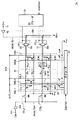
図16を図1と比較して、実施の形態2に従うMRAMデバイス1bにおいて、各ディジット線DLは、トランジスタスイッチ15を介して、メインディジット線MDLと接続される。メインディジット線MDLは、各ディジット線DLに共通に、かつ階層的に設けられた「上位書込配線」である。メインディジット線MDLには、電圧信号φ(DL)が印加される。
16 is compared with FIG. 1, each digit line DL is connected to main digit line MDL through
さらに、データ読出およびデータ書込に共用されるデータバスDBに代えて、データ書込専用のライトデータバスWDBが配置される。ライトデータバスWDBは、各ビット線BLに共通に、かつ階層的に設けられた「上位書込配線」である。 Further, a write data bus WDB dedicated to data writing is arranged instead of the data bus DB shared for data reading and data writing. The write data bus WDB is an “upper write wiring” provided in a hierarchical manner in common with each bit line BL.
書込バッファ70は、書込データDinに応じたデータ電圧をライトデータバスWDBに駆動する。ライトデータバスWDBは、各メモリセル列において、コラム選択スイッチ55を介して各ビット線BLと接続される。
Write
さらに、図示を省略しているが図1と同様のデータ読出アンプ80が設けられ、データ読出アンプと接続されるデータ読出用のリードデータバス(図示せず)がさらに設けられる。当該リードデータバスは、ライトデータバスWDBと接続されるコラム選択スイッチ55とは独立に設けられたリードコラム選択スイッチS3♯(図示せず)を介して、各ビット線BLと接続される。各リードコラム選択スイッチS3♯は、データ書込動作ではオフされる一方で、データ読出動作ではコラム選択線CSLに応答して、選択列でオンされる。これにより、図1におけるデータバスDBに代えて分離されたリードデータバスを用いて、データ読出が実行できる。
Further, although not shown, a data read
このように、ライトデータバスWDBをデータ読出経路から切り離すことにより、その容量を、データ書込動作に適合させて調整することが可能となる。逆に言えば、図1に示すように、データバスDBがデータ読出およびデータ書込で共用される構成においては、データバスDBの容量をデータ書込電流確保のために増加させると、データ読出動作速度が阻害されてしまう。 In this way, by separating the write data bus WDB from the data read path, the capacity can be adjusted to suit the data write operation. Conversely, as shown in FIG. 1, in the configuration in which data bus DB is shared for data reading and data writing, if the capacity of data bus DB is increased to secure the data writing current, data reading is performed. The operation speed is hindered.
実施の形態2によるMRAMデバイス1bのその他の部分の構成については、実施の形態1に従うMRAMデバイス1a(図1)と同様であるので詳細な説明は繰返さない。
Since the configuration of other parts of
図17は、この発明の実施の形態2に従うデータ書込電流供給構成を説明する概念図である。 FIG. 17 is a conceptual diagram illustrating a data write current supply configuration according to the second embodiment of the present invention.
図17を参照して、実施の形態2に従うデータ書込電流供給構成では、選択ディジット線DLiを始めとする各ディジット線は、スイッチ素子S2(トランジスタスイッチ15)を介して、メインディジット線MDLと接続される。符号61は、メインディジット線MDLの充電容量を示す。メインディジット線容量61は、メインディジット線MDLの寄生容量63aのみで構成されてもよいし、メインディジット線MDLと接続された容量素子(付加容量)63bと寄生容量63aとの和で構成されてもよい。
Referring to FIG. 17, in the data write current supply configuration according to the second embodiment, each digit line including selected digit line DLi is connected to main digit line MDL via switch element S2 (transistor switch 15). Connected.
さらに、選択ビット線BLjを始めとする各ビット線BLは、スイッチ素子S3(コラム選択スイッチ55)を介して、ライトデータバスWDBと接続される。実施の形態2による構成では、ライトデータバスWDBが書込ノード75に相当する。
Further, each bit line BL including the selected bit line BLj is connected to the write data bus WDB via the switch element S3 (column selection switch 55). In the configuration according to the second embodiment, write data bus WDB corresponds to write
符号66は、ライトデータバスWDBの充電容量を示す。ライトデータバス容量66は、ライトデータバスWDBの寄生容量68aのみで構成されてもよいし、ライトデータバスWDBに接続された容量素子(付加容量)68bと寄生容量68aとの和で構成されてもよい。
実施の形態2に従うデータ書込電流供給構成のその他の部分は、図4に示した実施の形態1に従うデータ書込電流供給構成と同様であるので、詳細な説明は繰り返さない。 Since the other parts of the data write current supply configuration according to the second embodiment are the same as those of the data write current supply configuration according to the first embodiment shown in FIG. 4, detailed description will not be repeated.
図18は、実施の形態2に従うMRAMデバイスの動作を説明する図である。 FIG. 18 is a diagram for explaining the operation of the MRAM device according to the second embodiment.
図18に示された動作シーケンスは、図6に示された実施の形態1に従う動作シーケンスに対応し、クロックサイクル1〜9における動作は図6に示した動作と同様である。
The operation sequence shown in FIG. 18 corresponds to the operation sequence according to the first embodiment shown in FIG. 6, and the operations in
すなわち、クロックサイクル1、3および9では、図6と同様のスタンバイ動作(Stby)が実行され、クロックサイクル2では、図6と同様のデータ読出動作(Read)が実行される。リードコラム選択スイッチS3♯はクロックサイクル2に選択ビット線でオンされる一方で、スタンバイ動作およびデータ書込動作では各ビット線BLにおいて、オフされる。
That is, in
クロックサイクル4〜8によって、データ“0”またはデータ“1”を書込むための単一のデータ書込動作(Write0またはWrite1)が構成される。 Clock cycles 4 to 8 constitute a single data write operation (Write 0 or Write 1) for writing data “0” or data “1”.
実施の形態2に従うデータ書込動作では、選択行のスイッチ素子S2は、メインディジット線容量61を選択ディジット線DLiの容量60と一体的に用いるために、選択ビット線BLjを再充電するクロックサイクル6を除いて、オン状態を維持される。選択列のスイッチ素子S3は、ライトデータバス容量66を選択ビット線BLjの容量65と一体的に用いるために、オン状態を維持される。一方、その他のスイッチ素子S1,S4a,S4bの動作は、図6に示された実施の形態1に従う動作と同様であるので、詳細な説明は繰り返さない。
In the data write operation according to the second embodiment, switch element S2 in the selected row uses clock cycle for recharging selected bit line BLj in order to use main
メインディジット線MDLに与えられる電圧信号φ(DL)は、スタンバイ動作(Stby)およびデータ読出動作(Read)が実行されるクロックサイクル1〜3,9と、データ書込動作中のディジット線DLの充電サイクル(クロックサイクル4,7)において電源電圧Vccに設定され、その他のクロックサイクルにおいてはハイインピーダンス状態(Z)とされる。
Voltage signal φ (DL) applied to main digit line MDL is applied to
このようなデータ書込シーケンスとすることにより、実施の形態2に従うMRAMデバイスにおいても、実施の形態1に従うMRAMデバイス1aと同様のデータ書込動作を実行できる。すなわち、MRAMデバイスの電源(バッテリ)から見た負荷電流パターンを緩やかなものに改善して、電源(バッテリ)からの電力供給可能期間を拡大することができる。 By adopting such a data write sequence, the MRAM device according to the second embodiment can execute the same data write operation as that of the MRAM device 1a according to the first embodiment. In other words, the load current pattern seen from the power source (battery) of the MRAM device can be improved to a gentle one, and the period in which power can be supplied from the power source (battery) can be extended.
さらに実施の形態2に従う構成においては、上位書込配線として設けられたメインディジット線MDLおよびライトデータバスWDBの容量を、ディジット線DLおよびビット線BLの充電容量として活用することができるので、当該充電容量の確保が容易となり、付加的な容量の設置による回路面積の増加を回避できる。 Furthermore, in the configuration according to the second embodiment, the capacity of main digit line MDL and write data bus WDB provided as the upper write wiring can be utilized as the charging capacity of digit line DL and bit line BL. It is easy to secure a charging capacity, and an increase in circuit area due to the installation of an additional capacity can be avoided.
[実施の形態2の変形例1]
実施の形態2に従うMRAMデバイスにおいて、実施の形態1の変形例1と同様に、ライトドライバを構成するスイッチ素子S4a,S4bを書込データDinに応じて制御して、データ書込動作の高速化を図ることも可能である。
[
In the MRAM device according to the second embodiment, as in the first modification of the first embodiment, the switch elements S4a and S4b constituting the write driver are controlled in accordance with the write data Din to increase the speed of the data write operation. It is also possible to plan.
図19は、実施の形態2の変形例1に従うMRAMデバイスの動作を説明する図である。 FIG. 19 is a diagram for explaining the operation of the MRAM device according to the first modification of the second embodiment.
図19に示された動作シーケンスは、図13に示された実施の形態1の変形例1に従う動作シーケンスに対応し、クロックサイクル1〜9における動作は図13に示した動作と同様である。 Operation sequence shown in FIG. 19 corresponds to the operation sequence according to the first modification of the first embodiment shown in FIG. 13, the operation in the clock cycles 1-9 are the same as the operations shown in FIG. 13.
すなわち、クロックサイクル1、3、6および9では、図13と同様のスタンバイ動作(Stby)が実行され、クロックサイクル2では、図13と同様のデータ読出動作(Read)が実行される。また、クロックサイクル4および5によって、データ“0”を書込むための単一のデータ書込動作(Write0)が構成され、クロックサイクル7および8によって、データ“1”を書込むための単一のデータ書込動作(Write1)が構成される。
That is, in
実施の形態2の変形例1に従うデータ書込動作においては、選択行のスイッチ素子S2は、メインディジット線容量61を選択ディジット線DLiの容量60と一体的に用いるために、オン状態を維持される。同様に、選択列のスイッチ素子S3は、ライトデータバス容量66を選択ビット線BLjの容量65と一体的に用いるために、オン状態を維持される。一方、その他のスイッチ素子S1,S4a,S4bの動作および書込ノード75の設定は、図13に示された実施の形態1の変形例1に従う動作シーケンスと同様であるので、詳細な説明は繰り返さない。
In the data write operation according to the first modification of the second embodiment, switch element S2 in the selected row is maintained in the ON state in order to use main
メインディジット線MDLに与えられる電圧信号φ(DL)は、スタンバイ動作(Stby)およびデータ読出動作(Read)が実行されるクロックサイクル1〜3,6,9と、データ書込動作中のディジット線DLの充電サイクル(クロックサイクル4,7)において電源電圧Vccに設定され、その他のクロックサイクルにおいてはハイインピーダンス状態(Z)とされる。 Voltage signal φ (DL) applied to main digit line MDL includes clock cycles 1 to 3, 6, and 9 in which standby operation (Stby) and data read operation (Read) are executed, and a digit line during data write operation. The power supply voltage Vcc is set in the DL charging cycle (clock cycles 4 and 7), and the high impedance state (Z) is set in the other clock cycles.
このようなデータ書込動作シーケンスとすることにより、実施の形態2に従うMRAMデバイスにおいて、実施の形態1の変形例1に従う構成と同様に、データ書込動作を高速化することができる。 By adopting such a data write operation sequence, in the MRAM device according to the second embodiment, the data write operation can be speeded up similarly to the configuration according to the first modification of the first embodiment.
[実施の形態2の変形例2]
図20は、この発明の実施の形態2の変形例2に従うデータ書込電流供給構成を説明する概念図である。
[
FIG. 20 is a conceptual diagram illustrating a data write current supply configuration according to the second modification of the second embodiment of the present invention.
図20を参照して、実施の形態2の変形例2に従うデータ書込電流供給構成では、図14に示した実施の形態1の変形例2に従うデータ書込構成と比較して、各ディジット線DLがスイッチ素子S2を介して、メインディジット線MDLと接続される点と、各ビット線BLがスイッチ素子S3を介してライトデータバスWDBと接続される点とが異なる。メインディジット線MDLには実施の形態2と同様の電圧信号φ(DL)が与えられ、メインディジット線MDLおよびライトデータバスWDBの容量はそれぞれ符号61および符号66で示される。
Referring to FIG. 20, in the data write current supply configuration according to the second modification of the second embodiment, each digit line is compared with the data write configuration according to the second modification of the first embodiment shown in FIG. The difference is that DL is connected to main digit line MDL via switch element S2 and bit line BL is connected to write data bus WDB via switch element S3. Main digit line MDL is supplied with voltage signal φ (DL) similar to that of the second embodiment, and the capacity of main digit line MDL and write data bus WDB are indicated by
実施の形態2の変形例2に従うデータ書込電流供給構成のその他の部分は、図14に示した実施の形態1の変形例2に従うデータ書込電流供給構成と同様であるので、詳細な説明は繰り返さない。 The other parts of the data write current supply configuration according to the second modification of the second embodiment are the same as those of the data write current supply configuration according to the second modification of the first embodiment shown in FIG. Will not repeat.
図21は、実施の形態2の変形例2に従うMRAMデバイスにおけるデータ書込動作を示すシーケンスである。 FIG. 21 is a sequence showing a data write operation in the MRAM device according to the second modification of the second embodiment.
図21に示された動作シーケンスは、図15に示された実施の形態1の変形例2に従う動作シーケンスに対応し、クロックサイクル1〜8における動作は図15に示した動作と同様である。
The operation sequence shown in FIG. 21 corresponds to the operation sequence according to the second modification of the first embodiment shown in FIG. 15, and the operation in
すなわち、クロックサイクル1、3および8では、図15と同様のスタンバイ動作(Stby)が実行され、クロックサイクル2では、図15と同様のデータ読出動作(Read)が実行される。また、クロックサイクル4〜7によって、データ“0”または“1”を書込むための単一のデータ書込動作(Write0またはWrite1)が構成される。
That is, in
実施の形態2の変形例2に従うデータ書込動作においても、選択行のスイッチ素子S2は、メインディジット線容量61を選択ディジット線DLiの容量60と一体的に用いるために、オン状態を維持される。同様に、選択列のスイッチ素子S3は、ライトデータバス容量66を選択ビット線BLjの容量65と一体的に用いるために、オン状態を維持される。一方、その他のスイッチ素子S1,S1♯,S4a,S4bの動作は、図15に示された実施の形態1の変形例2に従う動作シーケンスと同様であるので、詳細な説明は繰り返さない。
Also in the data write operation according to the second modification of the second embodiment, switch element S2 in the selected row is maintained in the ON state in order to use main
メインディジット線MDLに与えられる電圧信号φ(DL)は、スタンバイ動作(Stby)およびデータ読出動作(Read)が実行されるクロックサイクル1〜3,8と、データ書込動作中のディジット線DLの充電サイクル(クロックサイクル4)において電源電圧Vccに設定され、その他のクロックサイクルにおいてはハイインピーダンス状態(Z)とされる。
Voltage signal φ (DL) applied to main digit line MDL is applied to
このようなデータ書込シーケンスとすることにより、実施の形態2の変形例2に従うMRAMデバイスにおいて、実施の形態1の変形例2に従う構成と同様に、データ書込動作時のの各スイッチ素子のオン・オフ設定をパターン化して、ライトドライバ50の制御回路の構成を簡素化するとともに、データ書込動作に必要なクロックサイクル数を減じてデータ書込の高速化を図ることができる。
By adopting such a data write sequence, in the MRAM device according to the second modification of the second embodiment, each switch element at the time of the data write operation is similar to the configuration according to the second modification of the first embodiment. By patterning the on / off setting, the configuration of the control circuit of the
なお、実施の形態2ならびにその変形例1および2においては、各ディジット線DLに共通のメインディジット線MDLが設けられるが、メインディジット線容量61を調節するために、メインディジット線MDLを細分化して配置することも可能である。
In the second embodiment and its
たとえば、図22に示すように、メモリセルアレイ10に配置されたディジット線DLを、複数(たとえば4つ)のブロックBLK1〜BLK4に分割し、ブロックBLK1〜BLK4のそれぞれに対応させて、メインディジット線MDL1〜MDL4を分割配置することも可能である。メインディジット線MDLの分割数は、分割各された各メインディジット線の容量値が求められる値となるように、適宜定めることができる。
For example, as shown in FIG. 22, digit line DL arranged in
この場合には、トランジスタスイッチ15のオン・オフを制御する制御信号/DLPRを、ブロックBLK1〜BLK4にそれぞれ対応して、/DLPR(1)〜/DLPR(4)に独立に設定すれば、メインディジット線MDL1〜MDL4に与えられる電圧信号φ(DL)を共通のものとすることができる。
In this case, if the control signal / DLPR for controlling on / off of the
[実施の形態2の変形例3]
実施の形態2に従うMRAMデバイスにおいては、書込データDinによらず一定方向のデータ書込電流を供給するディジット線DLの充電容量が確保しやすくなるので、図10で説明したように、各ディジット線DLへの充電動作を制御するためのスイッチ素子S2の省略が可能となる。
[
In the MRAM device according to the second embodiment, it is easy to secure the charge capacity of digit line DL that supplies a data write current in a certain direction regardless of write data Din. Therefore, as described with reference to FIG. The switch element S2 for controlling the charging operation to the line DL can be omitted.
図23は、この発明の実施の形態2の変形例3に従うデータ書込電流供給構成を説明する概念図である。 FIG. 23 is a conceptual diagram illustrating a data write current supply configuration according to the third modification of the second embodiment of the present invention.
図23を参照して、実施の形態2の変形例3に従うデータ書込電流供給構成は、スイッチ素子S2の配置が省略されている点以外については、図17に示した実施の形態2に従うデータ書込電流供給構成と同様である。 Referring to FIG. 23, the data write current supply configuration according to the third modification of the second embodiment is similar to the data according to the second embodiment shown in FIG. 17 except that the arrangement of switch element S2 is omitted. This is the same as the write current supply configuration.
図24は、実施の形態2の変形例3に従うMRAMデバイスの動作を説明する図である。 FIG. 24 is a diagram illustrating the operation of the MRAM device according to the third modification of the second embodiment.
図24におけるクロックサイクル1〜9は、図18に示した実施の形態2に従うMRAMデバイスの動作シーケンスと同様であり、クロックサイクル1〜8のそれぞれにおける、書込ノード75の電圧設定、電圧信号φ(DL)の設定ならびにスイッチ素子S1,S3,S4a,S4bのオン・オフ設定は、図18に示した動作シーケンスと同様であるので詳細な説明は繰返さない。
Clock cycles 1 to 9 in FIG. 24 are similar to the operation sequence of the MRAM device according to the second embodiment shown in FIG. 18, and voltage setting and voltage signal φ of
このように、スイッチ素子S2の配置を省略しても、選択ディジット線DLiを、実施の形態2に従うMRAMデバイスにおけるデータ書込動作と同様に電源電圧Vccに充電できるので、同様の書込動作を実行することができる。 Thus, even if the arrangement of switch element S2 is omitted, select digit line DLi can be charged to power supply voltage Vcc similarly to the data write operation in the MRAM device according to the second embodiment. Can be executed.
特に、実施の形態2の変形例3による構成では、スイッチ素子S2の省略によって、メインディジット線容量61と、各ディジット線容量DLの和との総和が、データ書込電流Ipの供給に関する充電容量として一体的に利用できる。これにより、充電容量の確保がさらに容易となる。
In particular, in the configuration according to the third modification of the second embodiment, by omitting the switch element S2, the sum of the main
なお、図10でも説明したように、スイッチ素子S2の配置を省略した構成では、ディジット線DLの充電期間と、データ書込電流Ipの供給期間と完全に切離すデータ書込動作よりは、電源からの供給電力が若干増加する。しかしながら、スイッチ素子S2の配置が省略可能である点や、ディジット線DLの充電容量を容易に確保可能なことから、付加的な容量素子や充電調整抵抗の配置による回路面積の増加を回避できるので、回路面積の縮小に効果が大きい。 As described with reference to FIG. 10, in the configuration in which the arrangement of the switch element S2 is omitted, the power supply is more effective than the data write operation in which the digit line DL is completely disconnected from the charging period of the digit line DL and the supply period of the data write current Ip. The power supplied from will increase slightly. However, since the arrangement of the switch element S2 can be omitted and the charge capacity of the digit line DL can be easily secured, an increase in circuit area due to the arrangement of the additional capacity element and the charge adjustment resistor can be avoided. Greatly effective in reducing circuit area.
図25に示すように、実施の形態2の変形例3による構成においても、メインディジット線容量61を調節するために、メインディジット線MDLを細分化して配置することも可能である。
As shown in FIG. 25, also in the configuration according to the third modification of the second embodiment, in order to adjust the main
図25を参照して、メモリセルアレイ10上のディジット線DLは、図22と同様に複数(4つの)ブロックBLK1〜BLK4に分割され、ブロックBLK1〜BLK4のそれぞれに対応させて、メインディジット線MDL1〜MDL4が分割配置される。図22に示した構成と同等に、メインディジット線MDLの分割数は、分割各された各メインディジット線の容量値が求められる値となるように、適宜定めることができる。
Referring to FIG. 25, digit line DL on
この場合には、メインディジット線MDL1〜MDL4にそれぞれ与えられる電圧信号φ(DL)1〜φ(DL)4を独立に設定し、選択行が存在しないブロックにおいては、対応の電圧信号φ(DL)k(k:自然数)をハイインピーダンス状態にして、電源(バッテリ)からの電源供給を停止することが、電源の電力供給期間確保の観点からは好ましい。
In this case, voltage signals φ (DL) 1 to φ (DL) 4 applied to main
[実施の形態3]
図26は、この発明の実施の形態3に従うMRAMデバイス1cの全体構成を示す概略ブロック図である。
[Embodiment 3]
FIG. 26 is a schematic block diagram showing the overall configuration of the
図26を参照して、実施の形態3に従うMRAMデバイス1cは、図16に示した実施の形態2に従うMRAMデバイス1bと比較して、ビット線BLに対するデータ書込電流供給構成が一部異なる。具体的には、各ビット線BLの片端に対応して設けられるライトドライバ50に代えて、データバス/WDBおよびコラム選択スイッチ56が新たに設けられる。
Referring to FIG. 26,
ライトデータバス/WDBには、書込バッファ70♯によって、書込データDinの反転データ/Dinに応じたデータ電圧が駆動される。すなわち、書込バッファ70および70♯は、書込データDinに応じて、ライトデータバスWDBおよび/WDBにそれぞれ相補の電圧を駆動する。具体的には、Din=Hレベルのときには、ライトデータバスWDBが電源電圧Vccへ駆動される一方で、ライトデータバス/WDBは接地電圧Vssへ駆動される。反対に、Din=Lレベルのときには、ライトデータバスWDBが接地電圧Vssへ駆動される一方で、ライトデータバス/WDBは電源電圧Vccへ駆動される。
Data voltage corresponding to inverted data / Din of write data Din is driven by
ライトデータバス/WDBは、各メモリセル列において、対応のビット線BLとコラム選択スイッチ56を介して接続される。コラム選択スイッチ56のオン・オフは、同一メモリセル列のコラム選択スイッチ55と共通のコラム選択線CSLに応じて制御される。したがって、選択列においては、コラム選択スイッチ55および56の両方がオンされて、選択ビット線BLjはライトデータバスWDBおよび/WDBの間に接続される。一方非選択列においては、コラム選択スイッチ55および56の双方がターンオフされるので、ビット線BLはライトデータバスWDBおよび/WDBと非接続される。
Write data bus / WDB is connected to corresponding bit line BL via
また、実施の形態2の変形例3(図23)と同様に、各ディジット線DLにおけるスイッチ素子S2の配置が省略されて、各ディジット線DLは、電圧信号φ(DL)を受けるメインディジット線MDLと直接接続される。 Similarly to the third modification (FIG. 23) of the second embodiment, the arrangement of the switch element S2 in each digit line DL is omitted, and each digit line DL receives a main digit line that receives the voltage signal φ (DL). Directly connected to MDL.
実施の形態3によるMRAMデバイス1cのその他の部分の構成は、図16に示した実施の形態2によるMRAMデバイス1bと同様であるので詳細な説明は繰返さない。なお、図26においても、図16と同様にデータ読出系回路の記載を省略している。
Since the configuration of other parts of
図27は、この発明の実施の形態3に従うデータ書込電流供給構成を説明する概念図である。 FIG. 27 is a conceptual diagram illustrating a data write current supply configuration according to the third embodiment of the present invention.
図27を参照して、実施の形態3に従うデータ書込電流供給構成では、各ビット線BLは、スイッチ素子S3(コラム選択スイッチ55)を介してライトデータバスWDBと接続され、かつ、スイッチ素子S4(コラム選択スイッチ56)を介してライトデータバス/WDBと接続される。 Referring to FIG. 27, in the data write current supply configuration according to the third embodiment, each bit line BL is connected to write data bus WDB via switch element S3 (column selection switch 55), and switch element. It is connected to the write data bus / WDB via S4 (column selection switch 56).
符号66♯は、ライトデータバスWDBの充電容量を示す。ライトデータバス容量66♯は、ライトデータバスWDBの寄生容量69aのみで構成されてもよいし、ライトデータバスWDBに接続された容量素子(付加容量)69bと寄生容量69aとの和で構成されてもよい。
ディジット線DLに対するデータ書込電流の供給構成は、図23に示した実施の形態2の変形例3と同様であるので詳細な説明は繰返さない。
Since the structure for supplying data write current to digit line DL is similar to that of
図28は、実施の形態3に従うMRAMデバイスの動作を説明する図である。 FIG. 28 is a diagram for explaining the operation of the MRAM device according to the third embodiment.
図28を参照して、クロックサイクル1ではスタンバイ動作(Stby)が実行される。スタンバイ動作においては、各ディジット線DLを充電するために、メインディジット線MDLに与えられる電圧信号φ(DL)が電源電圧Vccに設定される。一方、スイッチ素子S1,S3,S4の各々がオフされてディジット線DLおよび各ビット線BLにはデータ書込電流は流れない。
Referring to FIG. 28, in
クロックサイクル2においては、データ読出動作(Read)が実行される。データ読出においても、各ビット線BLおよび各ディジット線DLにデータ書込電流を流す必要はないので、スイッチS1,S3,S4のオフ状態は維持されて、ディジット線DLは電源電圧Vccへの充電状態が維持される。
In
クロックサイクル3におけるスタンバイ動作についてはクロックサイクル1と同様である。
The standby operation in
クロックサイクル4および5によって、単一のデータ書込(Write)が実行される。まずクロックサイクル4においては、書込ノード75および76にそれぞれ相当するライトデータバスWDBおよび/WDBは、書込データDinおよびその反転データ/Dinにそれぞれ応じた電圧に充電される。たとえばDin=Lレベルとすると、ライトデータバスWDBの容量66は接地電圧Vssに充電され、ライトデータバス/WDBの容量66♯は電源電圧Vccに充電される。
Clock cycles 4 and 5 perform a single data write (Write). First, in
クロックサイクル4においても、スイッチ素子S1,S3,S4はオフ状態とされるので、各ディジット線DLおよび各ビット線BLにはデータ書込電流が生じない。すなわちこのクロックサイクルにおいては、選択ディジット線DLiに続いて、ライトデータバスWDBおよび/WDB、すなわち書込ノード75および76が、書込データDinに応じたデータ電圧レベルにそれぞれ充電される。
Also in
次のクロックサイクル5において、書込ノード75および76および電圧信号φ(DL)はハイインピーダンス状態(Z)とされ、かつ、スイッチ素子S1,S3,S4の各々がターンオンされる。これにより、選択ディジット線DLi上に、データ書込電流Ipが発生するとともに、選択ビット線BLj上にはデータ書込電流Iw(0)が生じる。
In
なお、書込データDin=Hレベルのときには、クロックサイクル4において、ライトデータバスWDBが電源電圧Vccに充電され、ライトデータバス/WDBが接地電圧Vssに充電されるので、クロックサイクル5において、スイッチ素子S3およびS4のターンオンに応答して、データ書込電流Iw(1)を選択ビット線BLj上に流すことができる。
When write data Din = H level, write data bus WDB is charged to power supply voltage Vcc and write data bus / WDB is charged to ground voltage Vss in
クロックサイクル6においては、クロックサイクル1および3と同様のスタンバイ動作が再び実行される。
In
このように実施の形態3に従うMRAMデバイスにおいては、実施の形態1および2と同様に、データ書込電流を供給するためにディジット線DLおよびライトデータバスWDB,/WDB(書込ノード75,76)を充電する動作と、実際にデータ書込電流IpおよびIw(0),Iw(1)を供給する動作とを独立に時分割して実行することができる。これにより、電源(バッテリ)からMRAMデバイスへ供給される負荷電流を緩やかなものとして、電力供給可能期間を拡大することができる。
As described above, in the MRAM device according to the third embodiment, digit line DL and write data buses WDB, / WDB (write
さらに実施の形態3に従う構成では、2クロックサイクルで単一のデータ書込動作を実行することができるため、データ書込動作の高速化についても効果がある。 Furthermore, in the configuration according to the third embodiment, since a single data write operation can be executed in two clock cycles, there is an effect in speeding up the data write operation.
なお、実施の形態3の説明では、各ディジット線DLの充電構成を実施の形態2の変形例3に従うMRAMデバイスと同様としたが、実施の形態1等と同様に、スイッチ素子S2を介して各ディジット線DLを充電する構成としてもよい。この場合には、スイッチ素子S2を、図25に示した動作シーケンスにおいて、少なくもクロックサイクル4でターンオンさせ、クロックサイクル5でオフさせる必要がある。また、実施の形態2で説明したように、メインディジット線MDLをブロックごとに分割する構成を採用してもよい。
In the description of the third embodiment, the charging configuration of each digit line DL is the same as that of the MRAM device according to the third modification of the second embodiment. However, similarly to the first embodiment and the like, via the switch element S2. A configuration may be employed in which each digit line DL is charged. In this case, the switch element S2 needs to be turned on at least in
[実施の形態4]
実施の形態4では、実施の形態1等で説明した、ビット線BLの両端にそれぞれライトドライバ50を設けることなくビット線BLへデータ書込電流を供給する構成に焦点をあてて説明する。
[Embodiment 4]
In the fourth embodiment, a description will be given focusing on the configuration described in the first embodiment and the like for supplying the data write current to the bit line BL without providing the
図29は、実施の形態4に従うMRAMデバイス1dのデータ書込構成を説明する概略ブロック図である。
FIG. 29 is a schematic block diagram illustrating a data writing configuration of
図29を参照して、実施の形態4に従うMRAMデバイス1dは、実施の形態2に従うMRAMデバイス1b(図16)と比較して、電圧駆動用の書込バッファ70に代えて、データ書込電流Iw(0),Iw(1)を供給するためのデータ書込回路100を備える点が異なる。さらに、各ディジット線DLについて電源電圧Vccへの充電構成は特に限定されないので、最も簡素な構成例として、各ディジット線DLがスイッチ素子を介さずに電源電圧Vccと直接接続される構成を示した。
Referring to FIG. 29,
データ書込回路100は、データ書込電流Iw(1)を供給するための定電流源110と、データ書込電流Iw(0)を供給するための定電流源120と、スイッチ素子112,122とを含む。スイッチ素子112は、定電流源110およびライトデータバスWDBの間に設けられる。スイッチ素子122は、定電流源120およびライトデータバスWDBの間に設けられる。
Data write
スイッチ素子112は、書込データDinがHレベルのときにオンし、Lレベルのときにオフする。これに対してスイッチ素子122は、反転された書込データ/Dinに応答して動作し、書込データDinがHレベルのときにオフし、Lレベルのときにオンする。
The
ライトドライバ50の構成および動作は、図1で説明したのと同様であるので詳細な説明は繰返さない。
Since the configuration and operation of
各ディジット線DLの一端側は、実施の形態2と同様に、行デコーダ20により行選択結果によってオン・オフするトランジスタスイッチ25を介して接地電圧Vssと接続されている。一方、各ディジット線DLの他端側は、充電期間の制御を考慮することなく、常時電源電圧Vccと接続される。
Similarly to the second embodiment, one end side of each digit line DL is connected to the ground voltage Vss through a
図30は、この発明の実施の形態4に従うデータ書込電流供給構成を説明する概念図である。 FIG. 30 is a conceptual diagram illustrating a data write current supply configuration according to the fourth embodiment of the present invention.
図30を参照して、ディジット線DLiの一端側は、スイッチ素子S1を介して接地電圧Vssと接続されており、スイッチ素子S1のターンオンに応答して、選択ディジット線DLiにデータ書込電流Ipを流すことができる。 Referring to FIG. 30, one end side of digit line DLi is connected to ground voltage Vss through switch element S1, and data write current Ip is applied to selected digit line DLi in response to turn-on of switch element S1. Can flow.
選択ビット線BLjの一端側は、コラム選択スイッチ55に相当するスイッチ素子S3のターンオンに応答して、ライトデータバスWDB(書込ノード75)と接続される。ライトデータバスWDBは、書込データDinに応じて選択的にターンオンされるスイッチ素子Sa(図29のスイッチ112に相当)およびスイッチ素子Sb(図29のスイッチ122に相当)によって、定電流源110および120のいずれか一方と接続される。
One end side of the selected bit line BLj is connected to the write data bus WDB (write node 75) in response to turning on of the switch element S3 corresponding to the
一方、選択ビット線BLjの他端側は、書込データDinに応じて選択的にオンされるスイッチ素子S4a(トランジスタスイッチ51に相当)およびスイッチ素子S4b(トランジスタスイッチ52に相当)によって、ライトデータバスWDBの設定電圧と相補的に、電源電圧Vccまたは接地電圧Vssと選択的に接続される。 On the other hand, the other end side of the selected bit line BLj is supplied with write data by a switch element S4a (corresponding to the transistor switch 51) and a switch element S4b (corresponding to the transistor switch 52) that are selectively turned on according to the write data Din. Complementary to the set voltage of bus WDB, it is selectively connected to power supply voltage Vcc or ground voltage Vss.
図31は、実施の形態4に従うMRAMデバイスでの書込動作を説明する図である。 FIG. 31 is a diagram illustrating a write operation in the MRAM device according to the fourth embodiment.
実施の形態4に従うMRAMデバイスにおいては、データ書込電流供給の準備のための充電期間と、データ電流供給期間とを特に区別することなく、両者は同時に実行可能である。 In the MRAM device according to the fourth embodiment, the charging period for preparing the data write current supply and the data current supply period can be executed simultaneously without any particular distinction.
書込データDin=Lレベル(Write0)のときには、選択ディジット線DLi上にデータ書込電流Ipを流すためにスイッチ素子S1がターンオンされるとともに、スイッチ素子S3,S4a,Sbがオンされる一方で、スイッチ素子S4b,Saがオフされる。 When write data Din = L level (Write0), switch element S1 is turned on to allow data write current Ip to flow through selected digit line DLi, while switch elements S3, S4a, and Sb are turned on. The switch elements S4b and Sa are turned off.
これにより、ライトデータバスWDB(書込ノード75)は、接地電圧Vssによって駆動される定電流源120と接続される。すなわち、ライトデータバスWDBは、接地電圧Vssに設定され、かつ、スイッチ素子S3を介して選択ビット線BLjの一端と接続される。さらに、ビット線BLjの他端はスイッチ素子S4aによって電源電圧Vccと接続される。これにより、選択ビット線BLj上には、定電流源120によって供給されるデータ書込電流Iw(0)が流される。
Thereby, write data bus WDB (write node 75) is connected to constant
これに対して、書込データDin=Hレベル(Write1)のときには、選択ディジット線DLi上にデータ書込電流Ipを流すためにスイッチ素子S1がターンオンされるとともに、スイッチ素子S3,S4b,Saがオンされる一方で、スイッチ素子S4a,Sbがオフされる。 On the other hand, when write data Din = H level (Write1), switch element S1 is turned on to cause data write current Ip to flow on selected digit line DLi, and switch elements S3, S4b, Sa On the other hand, the switch elements S4a and Sb are turned off.
これにより、ライトデータバスWDB(書込ノード75)は、電源電圧Vccによって駆動される定電流源110と接続される。すなわち、ライトデータバスWDBは、電源電圧Vccに設定され、かつ、スイッチ素子S3を介して選択ビット線BLjの一端と接続される。さらに、ビット線BLjの他端はスイッチ素子S4bよって接地電圧Vssと接続される。これにより、選択ビット線BLj上には、定電流源110によって供給されるデータ書込電流Iw(1)が流される。
Thereby, write data bus WDB (write node 75) is connected to constant
このような構成とすることにより、各ビット線BLの両端にライトドライバ50を配置する構成と比較して、ライトドライバ50の配置個数を削減できるので回路面積を縮小できる。
With such a configuration, the number of
また、実施の形態3のように、各ビット線BLの両端に相補のライトデータバスWDBおよび/WDBの両方を設ける構成では、ライトドライバ50の配置が省略可能な一方で、データ書込電流経路が長くなるので、寄生抵抗の増大により、データ書込電流の確保が困難になる可能性おそれがある。
In the configuration in which both the complementary write data buses WDB and / WDB are provided at both ends of each bit line BL as in the third embodiment, the arrangement of the
したがって、実施の形態4によるMRAMデバイスのように、ビット線BLの両側に、複数のスイッチ素子を含むライトドライバおよび、書込データに応じたデータ電圧に設定されるライトデータバスWDBをそれぞれ配置する構成とすることにより、回路面積の縮小と、データ書込電流経路の長大化防止によるデータ書込電流確保との両立を図ることが可能となる。 Therefore, like the MRAM device according to the fourth embodiment, the write driver including a plurality of switch elements and the write data bus WDB set to the data voltage corresponding to the write data are arranged on both sides of the bit line BL. By adopting the configuration, it is possible to achieve both reduction of the circuit area and securing of the data write current by preventing an increase in the length of the data write current path.
[実施の形態4の変形例]
図32は、実施の形態4の変形例に従うMRAMデバイス1eのデータ書込構成を説明する概略ブロック図である。
[Modification of Embodiment 4]
FIG. 32 is a schematic block diagram illustrating a data writing configuration of
図32を参照して、実施の形態4の変形例に従うMRAMデバイス1eは、実施の形態2に従うMRAMデバイス1b(図16)と比較して、電圧駆動用の書込バッファ70に代えて、複数本のビット線によって共有されるライトドライバ50♯を備える点が異なる。
Referring to FIG. 32, an
具体的には、MRAMデバイス1eでは、メモリセルアレイ10内の全ビット線は、複数本ずつのビット線グループ210に分割される。図32の構成例では、各ビット線グループ210は、2本のビット線(図32ではビット線BLj−1およびBLj)により構成される。
Specifically, in the
ビット線BLの一端側は、ビット線グループ210ごとに設けられたライトドライバ50♯と接続される。すなわち、ライトドライバ50♯は、同一のビット線グループ210に属する複数のビット線により共有される。
One end side of bit line BL is connected to a
ライトドライバ50♯は、ライトドライバ50と同様の構成を有し、トランジスタスイッチ51♯および52♯を含む。たとえば、トランジスタスイッチ51♯はpMOSトランジスタで構成され、トランジスタスイッチ52♯は、nMOSトランジスタで構成される。
Write
トランジスタスイッチ51♯のゲートには制御信号WDP♯が入力され、トランジスタスイッチ52のゲートには制御信号WDN♯が入力される。制御信号WDP♯,WDN♯は、各ビット線グループ210ごとに独立に生成される。図32には、第k番目(k:自然数)のビット線グループに対応する制御信号WDP♯k,WDN♯kが例示される。
Control signal WDP # is input to the gate of
ビット線BLの他端側は、各ビット線BLに対応して設けられるライトドライバ50と接続される。ライトドライバ50の構成および動作は、図1で説明したのと同様であるので詳細な説明は繰返さない。
The other end side of the bit line BL is connected to a
なお、図29に示したMRAMデバイス1dと同様に、各ディジット線DLについて電源電圧Vccへの充電構成は特に限定されないので、最も簡素な構成例として、各ディジット線DLがスイッチ素子を介さずに電源電圧Vccと直接接続される構成を示した。
Similarly to the
各ディジット線DLの一端側は、実施の形態2と同様に、行デコーダ20により行選択結果によってオン・オフするトランジスタスイッチ25を介して接地電圧Vssと接続されている。一方、各ディジット線DLの他端側は、充電期間の制御を考慮することなく、常時電源電圧Vccと接続される。
Similarly to the second embodiment, one end side of each digit line DL is connected to the ground voltage Vss through a
図33は、この発明の実施の形態4の変形例に従うデータ書込電流供給構成を説明する概念図である。 FIG. 33 is a conceptual diagram illustrating a data write current supply configuration according to a modification of the fourth embodiment of the present invention.
図33を参照して、ディジット線DLiの一端側は、スイッチ素子S1を介して接地電圧Vssと接続されており、スイッチ素子S1のターンオンに応答して、選択ディジット線DLiにデータ書込電流Ipを流すことができる。 Referring to FIG. 33, one end side of digit line DLi is connected to ground voltage Vss through switch element S1, and in response to turn-on of switch element S1, data write current Ip is supplied to selected digit line DLi. Can flow.
同一のビット線グループ210に属するビット線BLjおよびBLj−1の一端側は、ノード220で接続される。ノード220は、スイッチ素子S3aを介して電源電圧Vccと接続され、かつ、スイッチ素子S3bを介して接地電圧Vssと接続される。スイッチ素子S3aおよびS3bは、ライトドライバ50♯を構成するトランジスタスイッチ51♯および52♯(図32)にそれぞれ相当する。
One end sides of bit lines BLj and BLj−1 belonging to the same
一方、ビット線BLj−1およびBLjの他端側は、各ビット線BLに対応して設けられたスイッチ素子S3aおよびスイッチ素子S3bをそれぞれ介して、電源電圧Vccおよび接地電圧Vssと接続される。 On the other hand, the other end sides of bit lines BLj-1 and BLj are connected to power supply voltage Vcc and ground voltage Vss through switch elements S3a and S3b provided corresponding to each bit line BL, respectively.
図34は、実施の形態4の変形例に従うMRAMデバイスでの書込動作を説明する図である。 FIG. 34 illustrates a write operation in the MRAM device according to the modification of the fourth embodiment.
実施の形態4の変形例に従うMRAMデバイスにおいても、実施の形態4に従うMRAMデバイスと同様に、データ書込電流供給の準備のための充電期間と、データ電流供給期間とを特に区別することなく、両者は同時に実行可能である。 In the MRAM device according to the modification of the fourth embodiment, as in the MRAM device according to the fourth embodiment, the charging period for preparing the data write current supply and the data current supply period are not particularly distinguished, Both can be performed simultaneously.
対応のビット線が全て非選択のビット線グループにおいて、スイッチ素子S3a,S3bは両方ともオフされる。同様に、非選択のビット線では、スイッチ素子S4a,S4bは両方ともオフされる。また、非選択のディジット線に対応するスイッチ素子S1もオフされる。 In the bit line group in which all corresponding bit lines are not selected, both switch elements S3a and S3b are turned off. Similarly, in the non-selected bit line, both switch elements S4a and S4b are turned off. The switch element S1 corresponding to the non-selected digit line is also turned off.
これに対して、選択ビット線を含むビット線グループに対応するスイッチ素子S4a,S4bは、書込データに応じて一方がオンされ、他方がオフされる。さらに、選択ビット線に対応するスイッチ素子S3a,S3bは、選択ビット線の他端側がノード220の設定電圧と相補的に電源電圧Vccまたは接地電圧Vssと選択的に接続されるように、書込データに応じて一方がオンされ他方がオフされる。
On the other hand, one of switch elements S4a and S4b corresponding to the bit line group including the selected bit line is turned on and the other is turned off according to the write data. Further, the switch elements S3a and S3b corresponding to the selected bit line are written so that the other end side of the selected bit line is selectively connected to the power supply voltage Vcc or the ground voltage Vss complementarily to the set voltage of the
具体的には、書込データDin=Lレベル(Write0)のときには、選択ディジット線DLi上にデータ書込電流Ipを流すためにスイッチ素子S1がターンオンされるとともに、スイッチ素子S4a,S3bがオンされる一方で、スイッチ素子S4b,S3aがオフされる。 Specifically, when write data Din = L level (Write0), switch element S1 is turned on and switch elements S4a and S3b are turned on in order to flow data write current Ip on selected digit line DLi. On the other hand, the switch elements S4b and S3a are turned off.
これにより、ノード220はスイッチ素子S3bによって接地電圧Vssに設定される。一方、選択ビット線の他端はスイッチ素子S4aによって電源電圧Vccと接続される。これにより、選択ビット線上にデータ書込電流Iw(0)が流されて、選択メモリセルへデータ“0”が書込まれる。
Thereby, the
これに対して、書込データDin=Hレベル(Write1)のときには、選択ディジット線DLi上にデータ書込電流Ipを流すためにスイッチ素子S1がターンオンされるとともに、スイッチ素子S4b,S3aがオンされる一方で、スイッチ素子S4a,S3bがオフされる。 In contrast, when write data Din = H level (Write1), switch element S1 is turned on and switch elements S4b and S3a are turned on in order to flow data write current Ip on selected digit line DLi. On the other hand, the switch elements S4a and S3b are turned off.
これにより、ノード220はスイッチ素子S3aによって電源電圧Vccに設定される。一方、選択ビット線の他端はスイッチ素子S4bによって接地電圧Vssと接続される。これにより、選択ビット線上にデータ書込電流Iw(1)が流されて、選択メモリセルへデータ“1”が書込まれる。
Thereby,
このような構成とすることにより、ライトデータバスの配置によってデータ書込電流経路を長大化することなくデータ書込電流の確保を容易とした上で、各ビット線BLの両端にライトドライバ50を配置する構成と比較して、ライトドライバ50の配置個数を削減できるので回路面積を縮小できる。
With this configuration, it is easy to secure the data write current without increasing the data write current path by arranging the write data bus, and the
なお、図32〜図34では、各ビット線グループ210が2本のビット線を含む構成を例示したが、各ビット線グループは、任意の複数本のビット線によって構成することができる。
32 to 34 exemplify a configuration in which each
[実施の形態5]
図35は、実施の形態5に従うMRAMデバイス1fの全体構成を示す概略ブロック図である。
[Embodiment 5]
FIG. 35 is a schematic block diagram showing an overall configuration of MRAM device 1f according to the fifth embodiment.
図35を参照して、実施の形態5に従うMRAMデバイス1fは、実施の形態1に従うMRAMデバイス1aの構成に加えて、各ディジット線DLに対して設けられた定電流源130と、書込バッファ70に代えて設けられたデータ書込回路100とをさらに備える点で異なる。データ書込回路100の構成は、図29に示したのと同様であるが、定電流源110および120は、必要なデータ書込電流Iw(0)およびIw(1)の一部である定電流Iw0♯Iw1♯をそれぞれ供給する。
Referring to FIG. 35, in addition to the configuration of MRAM device 1a according to the first embodiment, MRAM device 1f according to the fifth embodiment includes a constant
また定電流源130は、対応のトランジスタスイッチ25のターンオン時に、対応のディジット線DLへ定電流Ip♯を流すことができる。定電流Ip♯は、必要なデータ書込電流Ipの一部に相当する。
Constant
図36は、この発明の実施の形態5に従うデータ書込電流供給構成を説明する概念図である。 FIG. 36 is a conceptual diagram illustrating a data write current supply configuration according to the fifth embodiment of the present invention.
図36を参照して、実施の形態5に従うデータ書込電流供給構成では、図4に示した実施の形態1に従うデータ書込電流供給構成と比較して、データ書込電流Ipの供給経路、すなわちスイッチ素子S1(トランジスタスイッチ25)および接地電圧Vssの間に定電流源130が配置される点と、書込ノード75に相当するライトデータバスWDBに対しては、図30に示した構成と同様に、定電流源110および120が書込データDinに応じて選択的に接続される点とで異なる。その他の部分については、図4に示した実施の形態1に従うデータ書込電流供給構成であるので、詳細な説明は繰り返さない。
Referring to FIG. 36, in the data write current supply configuration according to the fifth embodiment, compared with the data write current supply configuration according to the first embodiment shown in FIG. That is, for the point where constant
図37は、実施の形態5に従うMRAMデバイスの動作を説明する図である。 FIG. 37 is a diagram for explaining the operation of the MRAM device according to the fifth embodiment.
図37に示されるクロックサイクル1〜9では、図6に示したクロックサイクル1〜9と同様の動作が実行される。このため、スイッチ素子S1,S4a,S4bの動作は、図6に示したのと同様である。また、スタンバイ動作(Stby)およびデータ読出動作(Read)時すなわちクロックサイクル1〜3および9において、選択行および非選択行ともスイッチ素子S2はオンされる。
In
クロックサイクル4〜8は単一のデータ書込動作を構成する。単一のデータ書込動作では、データ“0”(Din=Lレベル)を書込む“Write0”およびデータ“1”(Din=Hレベル)を書込む“Write1”のいずれかが実行される。図37に示す例では、クロックサイクル4〜8により“Write0”が実行されるものとする。
Clock cycles 4-8 constitute a single data write operation. In a single data write operation, either “Write0” for writing data “0” (Din = L level) or “Write1” for writing data “1” (Din = H level) is executed. In the example shown in FIG. 37, “Write0” is executed in
一方、データ書込動作中(クロックサイクル4〜8)においては、非選択行のスイッチ素子S2がオフを維持される一方で、選択行のスイッチ素子S2は、選択ビット線を書込データに応じたデータ電圧に再充電するクロックサイクル6を除いてオンされる。
On the other hand, during the data write operation (clock cycles 4 to 8), switch element S2 in the non-selected row is kept off, while switch element S2 in the selected row uses the selected bit line according to the write data. It is turned on except for
さらに、データ書込回路100内のスイッチ素子SaおよびSbは、データ書込動作時以外にはターンオフされる一方で、データ書込動作時(クロックサイクル4〜8)には、書込データDinに応じて選択された一方が、スイッチ素子S1と対を成すようにオンする。すなわち、データ“0”の書込動作(Write“0”)においては、クロックサイクル4〜8を通じてスイッチ素子Saがオフされる一方で、スイッチ素子Sbは、クロックサイクル5および8にオンされる。図示しないが、データ“1”の書込動作(Write“1”)においては、クロックサイクル4〜8を通じてスイッチ素子Sbがオフされる一方で、スイッチ素子Saは、クロックサイクル5および8にオンされる。
Further, switch elements Sa and Sb in data write
さらに、スイッチ素子S3は、定電流源110,120を選択ビット線BLjと接続するために、データ書込動作時(クロックサイクル4〜8)には、オン状態に維持される。
Further, switch element S3 is maintained in the ON state during the data write operation (clock cycles 4 to 8) in order to connect constant
これにより、たとえばクロックサイクル4においては、実施の形態1と同様にディジット線容量60ならびにビット線容量65およびライトデータバス容量66の充電が行なわれ、クロックサイクル5においては、ディジット線容量60の放電電流および定電流源130による定電流Ip♯によって、選択ディジット線DLiにデータ書込電流Ipが流される。同様に、選択ビット線BLjには、ビット線容量65およびライトデータバス容量66からの充放電電流および定電流源120による定電流Iw0♯によって、データ書込電流Iw(0)が供給される。これにより、データ“0”が選択メモリセルへ書込まれる。
Thereby, for example, in
クロックサイクル6では、図6に示したクロックサイクル6と同様に、選択ビット線が書込データに応じたデータ電圧(接地電圧Vss)に再び充電される。
In
続くクロックサイクル7では、選択行のスイッチ素子S2がターンオンされて、選択ディジット線のディジット線容量が電源電圧Vccに再び充電されるが、スイッチ素子S1がオフされているので、データ書込電流Ipは流れない。また、スイッチ素子S4a,S4bがオフされるため、選択ビット線BLjの状態は、クロックサイクル6の終了時と同様に維持される。
In the
クロックサイクル8では、図6に示したクロックサイクル9と同様に、スイッチ素子S1,S4aがターンオンされるので、選択ディジット線上をデータ書込電流Ipが流れるが、選択ビット線BLjはその両端がそれぞれ電源電圧Vccと接続されることになるので、選択ビット線BLj上にデータ書込電流は流れない。
In
このようにして、クロックサイクル4〜8で構成される単一のデータ書込動作によって、クロックサイクル5でのデータ書込電流供給により、データ“0”(Din=Lレベル)のデータ書込が実行される。
In this way, data “0” (Din = L level) is written by supplying a data write current in
クロックサイクル9においては、クロックサイクル1,3,8と同様のスタンバイ動作(Stby)が実行される。
In
なお、“Write1”のデータ書込動作は、クロックサイクル4および6での書込ノード75の電圧設定を、Din=Hレベルに対応したデータ電圧(電源電圧Vcc)に変更した上で、スイッチ素子S1〜S3,S4a,S4bを“Write0”と同様にスイッチングさせるとともに、クロックサイクル5および8におけるスイッチ素子SaおよびSbのオン・オフを入れ替えることにより実行される。これにより、“Write1”では、クロックサイクル5では選択ビット線BLjにデータ書込電流が発生しない一方で、クロックサイクル8では選択ビット線BLjにデータ書込電流Iw(1)が流れることにより、選択メモリセルへデータ“1”が書込まれる。
Note that the data write operation of “Write1” is performed by changing the voltage setting of the
このように実施の形態5に従うMRAMデバイスでは、実施の形態1で説明した、ディジット線DLおよびビット線BLへの充電電荷による放電電流と、定電流源110,120,130による定電流との和によって、データ書込電流IpおよびIw(0),Iw(1)が供給される。
As described above, in the MRAM device according to the fifth embodiment, the sum of the discharge current due to the charge charged to the digit line DL and the bit line BL and the constant current by the constant
したがって、定電流源源110,120,130によって供給される定電流Iw1♯,Iw0♯,Ip♯は、ディジット線容量60やビット線容量65と、その充電電圧(電源電圧Vccおよび接地電圧Vssの電圧差に相当)との積、すなわち充電電荷によって供給可能な電流と、必要なデータ書込電流の電流量および印加時間の積との関係を考慮して、その不足分を補う範囲で設計すればよい。
Therefore, the constant currents Iw1 #, Iw0 #, and Ip # supplied by the constant
このような構成とすることにより、ディジット線容量60やビット線容量65に対して付加容量を設けて回路面積の増大を招くことなく、容易にデータ書込電流を確保することが可能となる。特に、データ書込電流の供給が容易化されることから、電源電圧Vccの低電圧化が可能となる。また、充電電荷の放電によりデータ書込電流の一部を供給することにより、定電流源源110,120,130を構成するトランジスタのサイズを縮小できるので、回路面積を縮小することも可能である。
By adopting such a configuration, it is possible to easily secure a data write current without increasing the circuit area by providing an additional capacitor for the
なお、実施の形態5に従うMRAMデバイス1eにおいては、実施の形態1に従うMRAMデバイス1aの構成に、定電流源110,120,130を追加配置した構成を示した。同様に、実施の形態1の変形例や、実施の形態2およびそれらの変形例に対しても、定電流源を追加配置して、充電電荷の放電と定電流源から供給される定電流との和によってデータ書込電流を供給する構成とすることが可能である。
In the
たとえば、図38には、実施の形態3に従うMRAMデバイスにおいて、ライトデータバスWDBおよび/WDBのそれぞれに対して、データ書込電流供給を補助するための定電流源が配置された構成が示される。 For example, FIG. 38 shows a configuration in which a constant current source for assisting data write current supply is arranged for each of write data buses WDB and / WDB in the MRAM device according to the third embodiment. .
図38を参照して、データバスWDBに対しては、図36と同様に、データ書込回路100が設けられる。すなわち、データバスWDBは、スイッチ素子SaおよびSbを介して、定電流源110および120と接続される。同様に、データバス/WDBに対しては、データ書込回路100♯が設けられる。データ書込回路100♯は、定電流源110♯および120♯と、スイッチ素子ScおよびSdとを含む。これにより、データバス/WDBは、スイッチ素子ScおよびSdを介して,定電流源110♯および120♯と接続される。スイッチ素子Scのオン・オフは、スイッチ素子Saと同様に、書込データDinに応じて制御され、スイッチ素子Sdのオン・オフは、スイッチ素子Sbと同様に、反転された書込データ/Dinに応じて制御される。
Referring to FIG. 38, data write
このような構成においては、図39に示すように、スイッチ素子S1、S3,S4のオン・オフについては、実施の形態3(図28)と同様に設定し、スイッチ素子S2については、図37と同様に、データ書込動作において選択行でオンし、非選択行でオフするように設定すればよい。さらに、定電流源110,120,110♯,120♯に対応して設けられるスイッチ素子Sa〜Sdについては、各データ書込動作期間内において、スイッチ素子S3,S4と同時に、書込データDinに応じて選択的にオンするように制御する。
In such a configuration, as shown in FIG. 39, on / off of the switch elements S1, S3, and S4 is set in the same manner as in the third embodiment (FIG. 28), and the switch element S2 is shown in FIG. Similarly to the above, in the data write operation, it may be set to be turned on in the selected row and turned off in the non-selected row. Further, switch elements Sa to Sd provided corresponding to constant
このような構成とすることにより、ディジット線容量60やビット線容量65に対して付加容量を設けて回路面積の増大を招くことがなく、かつ、定電流源110,110♯,120,120♯,130によって供給する定電流を抑制できる。したがって、実施の形態5に従うMRAMデバイスと同様の効果を供給することが可能である。
With such a configuration, an additional capacitor is provided for the
なお、以上の実施の形態では、データ書込系およびデータ読出系の両方に、共通の電源電圧Vccを用いたが、データ読出およびデータ書込で異なる電源電圧を用いることも可能である。また、電源電圧Vccについては、外部電源(たとえばバッテリ)から直接供給する構成とする他に、MRAM内部において、降圧回路(たとえば、差動増幅器を用いた一般的な構成のVDC:Voltage Down Converter)や昇圧回路(たとえば、一般的な構成のチャージポンプ回路)によって、データ読出/データ書込の電源電圧を生成する構成としてもよい。 In the above embodiment, the common power supply voltage Vcc is used for both the data writing system and the data reading system. However, different power supply voltages can be used for data reading and data writing. In addition, the power supply voltage Vcc is directly supplied from an external power supply (for example, a battery). In addition, in the MRAM, a step-down circuit (for example, a general configuration VDC: Voltage Down Converter using a differential amplifier) is provided. Alternatively, a power supply voltage for data reading / data writing may be generated by a booster circuit (for example, a charge pump circuit having a general configuration).
特に、チャージポンプ回路を採用すれば、一度に電源端子から大きな電流を供給することが困難なICカード用途等において、データ書込動作以外の期間を利用してデータ書込電流発生用の電源電圧を内部で生成できるため、データ書込電流の確保が容易となる。 In particular, if a charge pump circuit is used, a power supply voltage for generating a data write current using a period other than the data write operation in an IC card application where it is difficult to supply a large current from the power supply terminal at once. Can be generated internally, so that it is easy to secure the data write current.
また、「書込電流線」として設けられるディジット線DLおよびビット線BLに流れるデータ書込電流は、選択メモリセルへのデータ書込を実行するために必要な電流下限値と、周辺の非選択メモリセルへ誤書込が行なわれないための電流上限値との範囲内に設定する必要がある。特に、データ書込電流のピーク値は、回路上の寄生抵抗や寄生容量によって増大するのでその制御が困難である。このため、ディジット線DLおよびビット線BLについて、非特許文献4に開示されるような、金属配線の周囲3方向を薄い強磁性体で覆った配線を適用することにより、非選択メモリセルへの漏れ磁界を軽減して、データ誤書込の発生を抑制できる。
In addition, the data write current flowing in the digit line DL and the bit line BL provided as the “write current line” includes the current lower limit value necessary for executing data write to the selected memory cell and the peripheral non-selection. It is necessary to set within the range of the current upper limit value for preventing erroneous writing to the memory cell. In particular, the peak value of the data write current increases due to the parasitic resistance and parasitic capacitance on the circuit, and is difficult to control. Therefore, for the digit line DL and the bit line BL, by applying a wiring in which the three directions around the metal wiring are covered with a thin ferromagnet as disclosed in
以上説明した実施の形態1〜5およびそれらの変形例では、1ビットのデータ書込構成、すなわち1本の選択ビット線に書込データに応じたデータ書込電流が流される構成について説明したが、同様の構成について、複数ビットの並列なデータ書込構成にそれぞれ拡張することも可能である。 In the above-described first to fifth embodiments and the modifications thereof, the 1-bit data write configuration, that is, the configuration in which the data write current corresponding to the write data flows through one selected bit line has been described. The same configuration can be expanded to a parallel data writing configuration of a plurality of bits.
図40は、図4に示した実施の形態1に従うデータ書込電流供給構成を複数ビット書込に拡張した場合の構成を示す概念図である。 FIG. 40 is a conceptual diagram showing a configuration when the data write current supply configuration according to the first embodiment shown in FIG. 4 is extended to multi-bit writing.
図40を参照して、実施の形態1に従うデータ書込電流供給構成では、並列に書込むビット数に対応させて書込ノード75を複数個設けることにより、複数ビットの並列なデータ書込を実現できる。
Referring to FIG. 40, in the data write current supply configuration according to the first embodiment, by providing a plurality of
たとえば、2本の選択ビット線BLjおよびBLkにそれぞれ対応して独立の書込ノード75を設けた上で、図41に示すように、選択ビット線BLjおよびBLkに対応するスイッチ素子S3,S4a,S4bを同様のシーケンスで並列に動作させることにより、選択ビット線BLjおよびBLkのそれぞれに対して、独立の書込データを並列に書込める。
For example, after providing
図42に示すように、図14に示した実施の形態1の変形例2に従うデータ書込電流供給構成についても、並列に書込むビット数に対応させて書込ノード75を複数個設けることにより、同様に複数ビットの並列なデータ書込を実現できる。この場合にも、各書込ノードに対応する選択ビット線において、スイッチ素子S3,S4a,S4bを同様のシーケンスで並列に動作させればよい。また、図示しないが、実施の形態1の変形例1ならびに実施の形態2およびその変形例に従うデータ書込電流供給構成についても、書込ノード75を並列に書込むビット数に対応して複数個設けることにより、同様に複数ビットの並列なデータ書込を実現できる。
As shown in FIG. 42, the data write current supply configuration according to the second modification of the first embodiment shown in FIG. 14 is also provided by providing a plurality of
図43に示すように、図27に示した実施の形態3に従うデータ書込電流供給構成については、書込ノードに相当するライトデータバスWDB,/WDBの組を、並列に書込むビット数に対応させて複数個設けることにより、同様に複数ビットの並列なデータ書込を実現できる。この場合にも、各書込ノードに対応する選択ビット線において、スイッチ素子S3,S4を同様のシーケンスで並列に動作させればよい。 As shown in FIG. 43, in the data write current supply configuration according to the third embodiment shown in FIG. 27, the set of write data buses WDB, / WDB corresponding to the write node is set to the number of bits to be written in parallel. By providing a plurality of corresponding data, parallel data writing of a plurality of bits can be similarly realized. Also in this case, the switch elements S3 and S4 may be operated in parallel in the same sequence on the selected bit line corresponding to each write node.
図44に示すように、図30に示した実施の形態4に従うデータ書込電流供給構成については、ライトデータバスWDBおよびデータ書込回路100の組を並列に書込むビット数に対応して複数個設けることにより、同様に複数ビットの並列なデータ書込を実現できる。この場合にも、各書込ノードに対応する選択ビット線において、スイッチ素子S3,S4a,S4bを同様のシーケンスで並列に動作させればよい。
As shown in FIG. 44, the data write current supply configuration according to the fourth embodiment shown in FIG. 30 has a plurality of sets corresponding to the number of bits for writing the set of write data bus WDB and data write
図45に示すように、図33に示した実施の形態4の変形例に従うデータ書込電流供給構成については、並列に書込むビット数に対応した複数のビット線グループ210において、ライトドライバ50および50♯が選択ビット線をデータ電圧(VccまたはVss)と接続するように、スイッチ素子S3a,S3b,S4a,S4bのオン・オフ制御信号を生成すればよい。
As shown in FIG. 45, in the data write current supply configuration according to the modification of the fourth embodiment shown in FIG. 33, in the plurality of
さらに、図46に示すように、図36に示した実施の形態5に従うデータ書込電流供給構成についても、ライトデータバスWDBおよびデータ書込回路100の組を、並列に書込むビット数に対応させて複数個設けることにより、同様に複数ビットの並列なデータ書込を実現できる。この場合にも、各書込ノードに対応する選択ビット線において、スイッチ素子S3,S4a,S4b,Sa,Sbを同様のシーケンスで並列に動作させればよい。
Further, as shown in FIG. 46, the data write current supply configuration according to the fifth embodiment shown in FIG. 36 also corresponds to the number of bits in which the set of write data bus WDB and data write
また、図47に示すように、図38に示した実施の形態5に従うデータ書込電流供給構成についても、ライトデータバスWDBおよびデータ書込回路100の組ならびにライトデータバス/WDBおよびデータ書込回路100♯の組を、並列に書込むビット数に対応させて複数個設けることにより、同様に複数ビットの並列なデータ書込を実現できる。この場合にも、各書込ノードに対応する選択ビット線において、スイッチ素子S3,S4、Sa〜Sdを同様のシーケンスで並列に動作させればよい。
47, as for the data write current supply configuration according to the fifth embodiment shown in FIG. 38, the set of write data bus WDB and data write
今回開示された実施の形態はすべての点で例示であって制限的なものではないと考えられるべきである。本発明の範囲は上記した説明ではなくて特許請求の範囲によって示され、特許請求の範囲と均等の意味および範囲内でのすべての変更が含まれることが意図される。 The embodiment disclosed this time should be considered as illustrative in all points and not restrictive. The scope of the present invention is defined by the terms of the claims, rather than the description above, and is intended to include any modifications within the scope and meaning equivalent to the terms of the claims.
1a,1b,1c,1d,1e MRAMデバイス、10 メモリセルアレイ、15,25,51,52 トランジスタスイッチ、20 行デコーダ、30 列デコーダ、50,50♯ ライトドライバ、55,55r,56 コラム選択スイッチ、60 ディジット線容量、61 メインディジット線容量、62a,63a,67a,68a,69a 寄生容量、62b,63b,67b,68b,69b 付加容量、65 ビット線容量、66、66♯ ライトデータバス容量、70,70♯ 書込バッファ、71,71♯ データ端子、75,76 書込ノード、80 データ読出アンプ、100,100♯ データ書込回路、110,110♯,120,120♯,130 定電流源、112,122 スイッチ素子、BL ビット線、BLj 選択ビット線、BLK1〜BLK4 ブロック、CSL コラム選択線、DB データバス、DBr 参照データバス、Din 書込データ、/Din 反転データ、DL ディジット線、DLi 選択ディジット線、DMC ダミーメモリセル、Dout 読出データ、Ip,Iw(0),Iw(1) データ書込電流、Ip♯,Iw0♯,Iw1♯ 定電流、MC メモリセル、MDL,MDL1〜MDL4 メインディジット線、R0 充電抵抗、Rc 充電調整抵抗、Rp 放電抵抗、RWL リードワード線、S1〜S3,S4a,S4b,Sa〜Sd スイッチ素子、SL ソース線、TMR トンネル磁気抵抗素子、Vcc 電源電圧、Vss 所定電圧(接地電圧)、WDB,/WDB ライトデータバス、φ(DL) 電圧信号(メインディジット線)。 1a, 1b, 1c, 1d, 1e MRAM device, 10 memory cell array, 15, 25, 51, 52 transistor switch, 20 row decoder, 30 column decoder, 50, 50 # write driver, 55, 55r, 56 column select switch, 60 digit line capacity, 61 main digit line capacity, 62a, 63a, 67a, 68a, 69a parasitic capacity, 62b, 63b, 67b, 68b, 69b additional capacity, 65 bit line capacity, 66, 66 # write data bus capacity, 70 , 70 # write buffer, 71, 71 # data terminal, 75, 76 write node, 80 data read amplifier, 100, 100 # data write circuit, 110, 110 #, 120, 120 #, 130 constant current source, 112,122 Switch element, BL bit line, BLj selection Bit line, BLK1 to BLK4 block, CSL column selection line, DB data bus, DBr reference data bus, Din write data, / Din inverted data, DL digit line, DLi selection digit line, DMC dummy memory cell, Dout read data, Ip, Iw (0), Iw (1) Data write current, Ip #, Iw0 #, Iw1 # constant current, MC memory cell, MDL, MDL1 to MDL4 main digit line, R0 charging resistance, Rc charging adjustment resistance, Rp Discharge resistance, RWL read word line, S1 to S3, S4a, S4b, Sa to Sd switch element, SL source line, TMR tunnel magnetoresistive element, Vcc power supply voltage, Vss predetermined voltage (ground voltage), WDB, / WDB write data Bus, φ (DL) Voltage signal (Main Digi Door line).
Claims (4)
前記第1のデータ書込電流によって生じる磁界の印加によりデータが書き込まれる複数の磁気メモリセルと、
各前記第1の書込電流線の一端に対応して設けられた第1のスイッチ素子と、
各前記第1の書込電流線の他端に対応して設けられた第2のスイッチ素子とを備え、
前記第1のスイッチ素子は、第1の電圧に充電された状態である対応の前記第1の書込電流線を、前記第1の電圧とは異なる第2の電圧と接続することによって前記第1のデータ書込電流を生じさせ、
前記第2のスイッチ素子は、前記第1のスイッチ素子の非導通期間の少なくとも一部において導通して前記対応の第1の書込電流線および前記第1の電圧を電気的に接続し、かつ、前記第1のスイッチ素子の導通期間において非導通とされて前記対応の第1の書込電流線を前記第1の電圧から電気的に切り離す、薄膜磁性体記憶装置。 A plurality of first write current lines for selectively flowing a first data write current;
A plurality of magnetic memory cells into which data is written by application of a magnetic field generated by the first data write current;
A first switch element provided corresponding to one end of each of the first write current lines ;
A second switch element provided corresponding to the other end of each of the first write current lines ,
The first switch element connects the first write current line corresponding to a state charged with a first voltage to a second voltage different from the first voltage, thereby connecting the first switch element to the second voltage different from the first voltage. to cause one of the data write current,
The second switch element is electrically connected in at least part of a non-conduction period of the first switch element to electrically connect the corresponding first write current line and the first voltage; and A thin film magnetic memory device , wherein the first switch element is turned off during the conduction period to electrically disconnect the corresponding first write current line from the first voltage .
前記第1および前記第2のスイッチ素子の導通および非導通は、前記クロックサイクル毎に制御される、請求項1または2記載の薄膜磁性体記憶装置。3. The thin film magnetic memory device according to claim 1, wherein conduction and non-conduction of the first and second switch elements are controlled every clock cycle.
書込データに応じて、複数のデータ電圧のうちの1つに設定される書込ノードと、A write node set to one of a plurality of data voltages according to the write data;
各前記第2の書込電流線の一端に対応して設けられ、前記一端および前記書込ノードの間を電気的に接続するための第3のスイッチ素子と、A third switch element provided corresponding to one end of each of the second write current lines, for electrically connecting the one end and the write node;
各前記第2の書込電流線の他端を前記複数のデータ電圧とそれぞれ電気的に接続するための複数の第4のスイッチ素子とをさらに備え、A plurality of fourth switch elements for electrically connecting the other end of each of the second write current lines to the plurality of data voltages, respectively.
前記第1のデータ書込電流は、前記書込データによらず、選択された前記第1の書込電流線上を所定方向に流され、The first data write current is caused to flow in a predetermined direction on the selected first write current line regardless of the write data,
各前記磁気メモリセルは、前記第1のデータ書込電流および前記第2のデータ書込電流によってそれぞれ生じる磁界の組み合わせによって前記書込データを書き込まれ、Each of the magnetic memory cells is written with the write data by a combination of magnetic fields generated by the first data write current and the second data write current,
前記第3のスイッチ素子は、当該第3のスイッチ素子の導通によって対応の前記第2の書込電流線が前記書込ノードの電圧に充電された後に非導通とされ、The third switch element is turned off after the corresponding second write current line is charged to the voltage of the write node by the conduction of the third switch element,
前記第2のデータ書込電流は、前記複数の第4のスイッチ素子のうちの、前記書込ノードの電圧とは異なるデータ電圧に対応する1つが、前記第3のスイッチ素子の非導通後に導通することによって生じ、One of the plurality of fourth switch elements corresponding to a data voltage different from the voltage of the write node is turned on after the third switch element is turned off. Caused by
前記薄膜磁性体記憶装置は、基準クロック信号を受けて、前記基準クロック信号に応答してクロックサイクル毎に動作を実行するように構成され、The thin film magnetic memory device is configured to receive a reference clock signal and execute an operation every clock cycle in response to the reference clock signal,
前記クロックサイクルは、読出動作を実行するためのリードサイクルと、書込動作を実行するためのライトサイクルと、前記読出動作または前記書込動作に先立って実行されるスタンバイサイクルとを含み、The clock cycle includes a read cycle for executing a read operation, a write cycle for executing a write operation, and a standby cycle executed prior to the read operation or the write operation,
前記第2のスイッチ素子は、前記スタンバイサイクルにおいて導通するように制御される、請求項1記載の薄膜磁性体記憶装置。The thin film magnetic memory device according to claim 1, wherein the second switch element is controlled to be conductive in the standby cycle.
Priority Applications (3)
| Application Number | Priority Date | Filing Date | Title |
|---|---|---|---|
| JP2004112079A JP4553620B2 (en) | 2004-04-06 | 2004-04-06 | Thin film magnetic memory device |
| US11/099,669 US7272036B2 (en) | 2004-04-06 | 2005-04-06 | Thin film magnetic memory device suitable for drive by battery |
| US11/882,577 US7616476B2 (en) | 2004-04-06 | 2007-08-02 | Thin film magnetic memory device suitable for drive by battery |
Applications Claiming Priority (1)
| Application Number | Priority Date | Filing Date | Title |
|---|---|---|---|
| JP2004112079A JP4553620B2 (en) | 2004-04-06 | 2004-04-06 | Thin film magnetic memory device |
Related Child Applications (1)
| Application Number | Title | Priority Date | Filing Date |
|---|---|---|---|
| JP2010128910A Division JP2010186559A (en) | 2010-06-04 | 2010-06-04 | Thin film magnetic material storage apparatus |
Publications (3)
| Publication Number | Publication Date |
|---|---|
| JP2005302074A JP2005302074A (en) | 2005-10-27 |
| JP2005302074A5 JP2005302074A5 (en) | 2007-04-19 |
| JP4553620B2 true JP4553620B2 (en) | 2010-09-29 |
Family
ID=35054099
Family Applications (1)
| Application Number | Title | Priority Date | Filing Date |
|---|---|---|---|
| JP2004112079A Expired - Fee Related JP4553620B2 (en) | 2004-04-06 | 2004-04-06 | Thin film magnetic memory device |
Country Status (2)
| Country | Link |
|---|---|
| US (2) | US7272036B2 (en) |
| JP (1) | JP4553620B2 (en) |
Families Citing this family (15)
| Publication number | Priority date | Publication date | Assignee | Title |
|---|---|---|---|---|
| JP2007122838A (en) * | 2005-10-31 | 2007-05-17 | Toshiba Corp | Semiconductor storage device |
| DE102006032277B4 (en) * | 2006-07-12 | 2017-06-01 | Infineon Technologies Ag | Magnetic field sensor device |
| US20080137401A1 (en) * | 2006-12-07 | 2008-06-12 | Jan Boris Philipp | Memory that limits power consumption |
| US7852662B2 (en) * | 2007-04-24 | 2010-12-14 | Magic Technologies, Inc. | Spin-torque MRAM: spin-RAM, array |
| JP5096886B2 (en) * | 2007-11-20 | 2012-12-12 | シャープ株式会社 | Nonvolatile semiconductor memory device and driving method thereof |
| JP2009134794A (en) * | 2007-11-29 | 2009-06-18 | Renesas Technology Corp | Semiconductor device |
| US8081507B2 (en) * | 2008-09-25 | 2011-12-20 | Richard Lienau | Tri-state memory device and method |
| JP2012059326A (en) * | 2010-09-10 | 2012-03-22 | Toshiba Corp | Semiconductor storage device |
| JP5916524B2 (en) * | 2012-06-07 | 2016-05-11 | ルネサスエレクトロニクス株式会社 | Semiconductor device |
| US9804793B2 (en) * | 2016-03-04 | 2017-10-31 | Intel Corporation | Techniques for a write zero operation |
| TWI609379B (en) * | 2016-04-26 | 2017-12-21 | 來揚科技股份有限公司 | Peak current bypass protection control device applicable in mram |
| CN107404112A (en) * | 2016-05-18 | 2017-11-28 | 来扬科技股份有限公司 | Peak current bypass protection control device applied to MRAM |
| TWI693766B (en) * | 2018-04-18 | 2020-05-11 | 力旺電子股份有限公司 | Electrostatic discharge protection device |
| KR102651232B1 (en) | 2019-07-18 | 2024-03-25 | 삼성전자주식회사 | Magnetic junction memory device and method for reading data from the memory device |
| KR102651229B1 (en) | 2019-07-22 | 2024-03-25 | 삼성전자주식회사 | Magnetic junction memory device and method for writing data to the memory device |
Citations (2)
| Publication number | Priority date | Publication date | Assignee | Title |
|---|---|---|---|---|
| JP2002231904A (en) * | 2001-02-06 | 2002-08-16 | Mitsubishi Electric Corp | Magnetic storage system and magnetic substrate |
| WO2003054887A1 (en) * | 2001-12-20 | 2003-07-03 | Micron Technology Inc. | A programmable conductor random access memory and a method for writing thereto |
Family Cites Families (6)
| Publication number | Priority date | Publication date | Assignee | Title |
|---|---|---|---|---|
| GB1376995A (en) * | 1972-01-14 | 1974-12-11 | Elliott Brothers London Ltd | Magnetic data storage arrangements |
| US6034887A (en) | 1998-08-05 | 2000-03-07 | International Business Machines Corporation | Non-volatile magnetic memory cell and devices |
| JP4780874B2 (en) * | 2001-09-04 | 2011-09-28 | ルネサスエレクトロニクス株式会社 | Thin film magnetic memory device |
| US6643213B2 (en) * | 2002-03-12 | 2003-11-04 | Hewlett-Packard Development Company, L.P. | Write pulse circuit for a magnetic memory |
| WO2004061854A1 (en) * | 2003-01-06 | 2004-07-22 | Nec Corporation | Semiconductor memory device |
| JP4290494B2 (en) | 2003-07-08 | 2009-07-08 | 株式会社ルネサステクノロジ | Semiconductor memory device |
-
2004
- 2004-04-06 JP JP2004112079A patent/JP4553620B2/en not_active Expired - Fee Related
-
2005
- 2005-04-06 US US11/099,669 patent/US7272036B2/en not_active Expired - Fee Related
-
2007
- 2007-08-02 US US11/882,577 patent/US7616476B2/en active Active
Patent Citations (2)
| Publication number | Priority date | Publication date | Assignee | Title |
|---|---|---|---|---|
| JP2002231904A (en) * | 2001-02-06 | 2002-08-16 | Mitsubishi Electric Corp | Magnetic storage system and magnetic substrate |
| WO2003054887A1 (en) * | 2001-12-20 | 2003-07-03 | Micron Technology Inc. | A programmable conductor random access memory and a method for writing thereto |
Also Published As
| Publication number | Publication date |
|---|---|
| US20070285977A1 (en) | 2007-12-13 |
| US7616476B2 (en) | 2009-11-10 |
| JP2005302074A (en) | 2005-10-27 |
| US20050219894A1 (en) | 2005-10-06 |
| US7272036B2 (en) | 2007-09-18 |
Similar Documents
| Publication | Publication Date | Title |
|---|---|---|
| KR100505769B1 (en) | Thin film magnetic memory device provided with a dummy cell for data read reference | |
| US7272036B2 (en) | Thin film magnetic memory device suitable for drive by battery | |
| JP4290494B2 (en) | Semiconductor memory device | |
| US7295465B2 (en) | Thin film magnetic memory device reducing a charging time of a data line in a data read operation | |
| KR100654266B1 (en) | Thin film magnetic memory device having magnetic tunnel junction | |
| US7885096B2 (en) | Thin film magnetic memory device writing data with bidirectional current | |
| JP4046513B2 (en) | Semiconductor integrated circuit | |
| JP4208498B2 (en) | Thin film magnetic memory device | |
| US20030107916A1 (en) | Thin film magnetic memory device conducting data read operation without using a reference cell | |
| JP5230783B2 (en) | Thin film magnetic memory device | |
| JP4262954B2 (en) | Thin film magnetic memory device | |
| JP2008084533A (en) | Thin magnetic film storage device | |
| US20040151052A1 (en) | Semiconductor memory device with magnetic disturbance reduced | |
| JP2010186559A (en) | Thin film magnetic material storage apparatus | |
| JP4712779B2 (en) | Thin film magnetic memory device |
Legal Events
| Date | Code | Title | Description |
|---|---|---|---|
| A521 | Written amendment |
Free format text: JAPANESE INTERMEDIATE CODE: A523 Effective date: 20070302 |
|
| A621 | Written request for application examination |
Free format text: JAPANESE INTERMEDIATE CODE: A621 Effective date: 20070302 |
|
| A131 | Notification of reasons for refusal |
Free format text: JAPANESE INTERMEDIATE CODE: A131 Effective date: 20100406 |
|
| A711 | Notification of change in applicant |
Free format text: JAPANESE INTERMEDIATE CODE: A712 Effective date: 20100519 |
|
| A521 | Written amendment |
Free format text: JAPANESE INTERMEDIATE CODE: A523 Effective date: 20100604 |
|
| TRDD | Decision of grant or rejection written | ||
| A01 | Written decision to grant a patent or to grant a registration (utility model) |
Free format text: JAPANESE INTERMEDIATE CODE: A01 Effective date: 20100706 |
|
| A01 | Written decision to grant a patent or to grant a registration (utility model) |
Free format text: JAPANESE INTERMEDIATE CODE: A01 |
|
| A61 | First payment of annual fees (during grant procedure) |
Free format text: JAPANESE INTERMEDIATE CODE: A61 Effective date: 20100713 |
|
| FPAY | Renewal fee payment (event date is renewal date of database) |
Free format text: PAYMENT UNTIL: 20130723 Year of fee payment: 3 |
|
| R150 | Certificate of patent or registration of utility model |
Ref document number: 4553620 Country of ref document: JP Free format text: JAPANESE INTERMEDIATE CODE: R150 Free format text: JAPANESE INTERMEDIATE CODE: R150 |
|
| S531 | Written request for registration of change of domicile |
Free format text: JAPANESE INTERMEDIATE CODE: R313531 |
|
| R350 | Written notification of registration of transfer |
Free format text: JAPANESE INTERMEDIATE CODE: R350 |
|
| LAPS | Cancellation because of no payment of annual fees |