JP2006289999A - Thermal head and method for manufacturing thermal head - Google Patents
Thermal head and method for manufacturing thermal head Download PDFInfo
- Publication number
- JP2006289999A JP2006289999A JP2006207374A JP2006207374A JP2006289999A JP 2006289999 A JP2006289999 A JP 2006289999A JP 2006207374 A JP2006207374 A JP 2006207374A JP 2006207374 A JP2006207374 A JP 2006207374A JP 2006289999 A JP2006289999 A JP 2006289999A
- Authority
- JP
- Japan
- Prior art keywords
- head
- chip
- thermal head
- wiring board
- wiring
- Prior art date
- Legal status (The legal status is an assumption and is not a legal conclusion. Google has not performed a legal analysis and makes no representation as to the accuracy of the status listed.)
- Granted
Links
Images


Abstract
Description
本発明は、例えば、小型携帯用記録装置、ファックス、切符及びレシートの印刷装置などに用いられるサーマルヘッド及びサーマルヘッドユニット並びにその製造方法に関する。 The present invention relates to a thermal head and a thermal head unit used in, for example, a small portable recording apparatus, a fax machine, a ticket and a receipt printing apparatus, and a manufacturing method thereof.
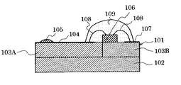
背景技術 サーマルヘッドは、一列に並んだ発熱体及びこれらに接続される電極をセラミック基板上に有するヘッドチップと、所定の発熱体を所定のタイミングで選択的に発熱させるための印字信号を出力するドライバとなるICチップとを有する。 このようなサーマルヘッドを放熱板上に搭載してユニット化したサーマルヘッドユニットの一例を図19に示す。このサーマルヘッドユニットは、サーマルヘッド101と、アルミニウム等からなる放熱板102とから構成される。サーマルヘッド101は、セラミック基板103上に、電極104及び発熱体105を形成し、さらに、ICチップ106を搭載したものである。なお、電極104、及び別途設けられた外部信号入力用の外部端子107と、ICチップ106とは、ボンディングワイヤ108を介してそれぞれ接続されており、ICチップ106及びボンディングワイヤ108は、封止樹脂109でモールドされている。
BACKGROUND ART A thermal head outputs a print signal for selectively heating a predetermined heating element at a predetermined timing, with a head chip having a heating element arranged in a row and electrodes connected to the ceramic chip on a ceramic substrate. An IC chip serving as a driver. FIG. 19 shows an example of a thermal head unit in which such a thermal head is mounted on a heat sink and unitized. This thermal head unit includes a
このようなサーマルヘッド101は、基板工程において、比較的大きなセラミック基板103を用いて薄膜又は厚膜により電極104及び発熱体105等を形成するため、一工程での取り数が小さく、生産性が悪いという問題がある。
Such a
そこで、基板工程での生産性を向上させるために、セラミック基板を小さくして複合基板とした構造も知られている。すなわち、図20に示すように、セラミック基板103の代わりに、セラミック基板103A及びガラス布基材エポキシ樹脂基板(以下、ガラエポ基板という)などの配線基板103Bを用い、この場合には、外部端子107を配線基板103B上に設けたものである。
Therefore, in order to improve the productivity in the substrate process, a structure in which the ceramic substrate is reduced to form a composite substrate is also known. That is, as shown in FIG. 20, instead of the
しかしながら、この場合には、基板工程の生産性は向上するものの、セラミック基板103A及び配線基板103Bを放熱板102に接合した後、ICチップ106の搭載及びワイヤボンディングを行わなければならないので、ハンドリング性が大幅に低下するという問題がある。
However, in this case, although the productivity of the substrate process is improved, since the
そこで、本発明は、このような事情に鑑み、基板工程の生産性を向上させると共に、実装工程のハンドリング性を向上させ、大幅なコストダウンを図ることができるサーマルヘッド及びサーマルヘッドユニット並びにその製造方法を提供することを課題とする。 Therefore, in view of such circumstances, the present invention improves the productivity of the substrate process, improves the handling process of the mounting process, and can significantly reduce the cost, and the manufacturing thereof. It is an object to provide a method.
前記課題を解決する本発明の第1の態様は、一方面に発熱体及び該発熱体に接続される電極を有するヘッドチップと、前記電極に接続される半導体集積回路とを具備するサーマルヘッドにおいて、前記ヘッドチップの他方面に接合される配線基板を具備し、前記半導体集積回路を前記配線基板に搭載してなることを特徴とするサーマルヘッドにある。 A first aspect of the present invention for solving the above-described problem is a thermal head comprising a head chip having a heating element and an electrode connected to the heating element on one surface, and a semiconductor integrated circuit connected to the electrode. A thermal head comprising a wiring board bonded to the other surface of the head chip, wherein the semiconductor integrated circuit is mounted on the wiring board.
本発明の第2の態様は、第1の態様において、前記ヘッドチップの幅方向一端側が前記配線基板から突出していることを特徴とするサーマルヘッドにある。 According to a second aspect of the present invention, there is provided the thermal head according to the first aspect, wherein one end side in the width direction of the head chip protrudes from the wiring board.
本発明の第3の態様は、第2の態様において、前記ヘッドチップの前記配線基板からの突出量が当該ヘッドチップの幅の20%〜70%であることを特徴とするサーマルヘッドにある。 According to a third aspect of the present invention, there is provided the thermal head according to the second aspect, wherein the protruding amount of the head chip from the wiring board is 20% to 70% of the width of the head chip.
本発明の第4の態様は、第1の態様において、前記ヘッドチップは、前記配線基板上に完全に重なって接合されていることを特徴とするサーマルヘッドにある。 According to a fourth aspect of the present invention, there is provided the thermal head according to the first aspect, wherein the head chip is completely overlapped and bonded onto the wiring board.
本発明の第5の態様は、第4の態様において、前記ヘッドチップの幅方向一端側より前記配線基板の一端側が突出していることを特徴とするサーマルヘッドにある。 A fifth aspect of the present invention is the thermal head according to the fourth aspect, wherein one end side of the wiring substrate protrudes from one end side in the width direction of the head chip.
本発明の第6の態様は、第1〜5の何れかの態様において、前記半導体集積回路は、前記ヘッドチップの端面に実質的に接触して前記配線基板上に搭載されていることを特徴とするサーマルヘッドにある。 According to a sixth aspect of the present invention, in any one of the first to fifth aspects, the semiconductor integrated circuit is mounted on the wiring board substantially in contact with an end face of the head chip. It is in the thermal head.
本発明の第7の態様は、第1〜6の何れかの態様において、前記半導体集積回路の表面の高さが、前記ヘッドチップの表面の高さと略同一であることを特徴とするサーマルヘッドにある。 According to a seventh aspect of the present invention, in any one of the first to sixth aspects, the height of the surface of the semiconductor integrated circuit is substantially the same as the height of the surface of the head chip. It is in.
本発明の第8の態様は、第1〜6の何れかの態様において、前記半導体集積回路の表面の高さが、前記ヘッドチップの表面の高さより低いことを特徴とするサーマルヘッドにある。 An eighth aspect of the present invention is the thermal head according to any one of the first to sixth aspects, wherein the height of the surface of the semiconductor integrated circuit is lower than the height of the surface of the head chip.
本発明の第9の態様は、第1〜8の何れかの態様において、前記ヘッドチップの前記発熱体とは反対側の幅方向端部に沿って長手方向に亘って共通電極を有し、当該共通電極と前記配線基板に設けられた共通電極用配線とを接続する接続配線が長手方向に亘っての複数箇所に設けられていることを特徴とするサーマルヘッドにある。
本発明の第10の態様は、第9の態様において、前記ヘッドチップに設けられた共通電極と前記配線基板に設けられた共通電極用配線とを接続する接続配線が、前記半導体集積回路により規定される物理ブロックの間に設けられていることを特徴とするサーマルヘッドにある。
According to a ninth aspect of the present invention, in any one of the first to eighth aspects, the head chip has a common electrode along a longitudinal direction along an end portion in a width direction opposite to the heating element, The thermal head is characterized in that connection wiring for connecting the common electrode and the wiring for the common electrode provided on the wiring board is provided at a plurality of positions in the longitudinal direction.
According to a tenth aspect of the present invention, in the ninth aspect, a connection wiring for connecting the common electrode provided on the head chip and the common electrode wiring provided on the wiring board is defined by the semiconductor integrated circuit. The thermal head is provided between physical blocks.
本発明の第11の態様は、第10の態様において、前記ヘッドチップに設けられた共通電極と前記配線基板に設けられた共通電極用配線とを接続する接続配線が、前記半導体集積回路により規定される物理ブロック毎に設けられていることを特徴とするサーマルヘッドにある。 According to an eleventh aspect of the present invention, in the tenth aspect, a connection wiring for connecting a common electrode provided on the head chip and a common electrode wiring provided on the wiring board is defined by the semiconductor integrated circuit. The thermal head is provided for each physical block.
本発明の第12の態様は、第9〜11の何れかの態様において、前記ヘッドチップに設けられた共通電極と前記配線基板に設けられた共通電極用配線とを接続する接続配線が、前記半導体集積回路により規定される物理ブロック内に少なくとも一つ設けられていることを特徴とするサーマルヘッドにある。 According to a twelfth aspect of the present invention, in any one of the ninth to eleventh aspects, the connection wiring that connects the common electrode provided on the head chip and the common electrode wiring provided on the wiring board includes: The thermal head is provided with at least one physical block defined by a semiconductor integrated circuit.
本発明の第13の態様は、第1〜12の何れかの態様のサーマルヘッドを支持体に搭載してなることを特徴とするサーマルヘッドユニットにある。 A thirteenth aspect of the present invention is a thermal head unit comprising the thermal head according to any one of the first to twelfth aspects mounted on a support.
本発明の第14の態様は、第13の態様において、前記サーマルヘッドは、前記ヘッドチップの幅方向一端部の発熱体形成部が前記配線基板から突出しており、前記支持体には前記発熱体形成部が接合される上段部と該上段部より前記配線基板の厚さより深く凹んだ段差部とが形成され、前記ヘッドチップの前記発熱体形成部と前記上段部とを接合したときに前記段差部と前記配線基板との間に生じる隙間に接着剤層が設けられていることを特徴とするサーマルヘッドユニットにある。 According to a fourteenth aspect of the present invention, in the thirteenth aspect, in the thermal head, the heating element forming portion at one end in the width direction of the head chip protrudes from the wiring board, and the heating element is provided on the support body. An upper step portion to which the forming portion is bonded and a step portion that is recessed deeper than the thickness of the wiring board from the upper step portion are formed, and the step when the heating element forming portion and the upper step portion of the head chip are bonded. The thermal head unit is characterized in that an adhesive layer is provided in a gap formed between the wiring portion and the wiring board.
本発明の第15の態様は、第14の態様において、前記ヘッドチップの前記発熱体形成部と前記上段部とを接合する接着層を具備し、前記発熱体形成部と前記上段部との接合後で前記接着剤層の硬化前に、前記接着剤層が前記接着層より柔らかいことを特徴とするサーマルヘッドユニットにある。 According to a fifteenth aspect of the present invention, in the fourteenth aspect, the fifteenth aspect includes an adhesive layer that joins the heating element forming portion and the upper step portion of the head chip, and bonding the heating element forming portion and the upper step portion. In the thermal head unit, the adhesive layer is softer than the adhesive layer later before the adhesive layer is cured.
本発明の第16の態様は、第14又は15の態様において、前記ヘッドチップの前記発熱体形成部と前記上段部とを接合する接着層を具備し、当該接着層より前記接着剤層が厚いことを特徴とするサーマルヘッドユニットにある。 According to a sixteenth aspect of the present invention, in the fourteenth or fifteenth aspect, the sixteenth aspect includes an adhesive layer that joins the heating element forming portion and the upper step portion of the head chip, and the adhesive layer is thicker than the adhesive layer. It is in the thermal head unit characterized by the above.
本発明の第17の態様は、第14〜16の何れかの態様において、前記段差部の底部には、さらに凹んだ溝が少なくとも一つ設けられていることを特徴とするサーマルヘッドユニットにある。 A seventeenth aspect of the present invention is the thermal head unit according to any one of the fourteenth to sixteenth aspects, wherein at least one recessed groove is provided at the bottom of the stepped portion. .
本発明の第18の態様は、一方面に発熱体及び該発熱体に接続される電極を有するセラミック基板と、前記ヘッドチップの他方面に接合される配線基板とを具備し、半導体集積回路を前記配線基板に搭載してなるサーマルヘッドの製造方法において、前記配線基板を複数個取り可能な配線基板用プレート上に、複数個の前記ヘッドチップを接合する工程と、複数の前記半導体集積回路を前記配線基板用プレートに搭載する工程と、前記ヘッドチップ上の前記電極と前記半導体集積回路とを配線する工程と、前記配線基板用プレートを複数個に分割する工程とを具備することを特徴とするサーマルヘッドの製造方法にある。
本発明の第19の態様は、第18の態様において、前記ヘッドチップは、前記配線基板用プレートに一方向に向いて縦横複数列ずつ並設されることを特徴とするサーマルヘッドの製造方法にある。
According to an eighteenth aspect of the present invention, there is provided a semiconductor integrated circuit comprising a ceramic substrate having a heating element on one side and an electrode connected to the heating element, and a wiring board bonded to the other side of the head chip. In the method of manufacturing a thermal head mounted on the wiring board, a step of bonding a plurality of the head chips on a wiring board plate capable of taking a plurality of the wiring boards, and a plurality of the semiconductor integrated circuits Mounting the wiring board plate, wiring the electrode on the head chip and the semiconductor integrated circuit, and dividing the wiring board plate into a plurality of parts. There is a method for manufacturing a thermal head.
According to a nineteenth aspect of the present invention, in the method for manufacturing a thermal head according to the eighteenth aspect, the head chips are arranged in parallel in a plurality of vertical and horizontal rows in one direction on the wiring board plate. is there.
本発明の第20の態様は、第19の態様において、前記ヘッドチップの一部は、前記一方向とは直交する方向に向いて接合されることを特徴とするサーマルヘッドの製造方法にある。 According to a twentieth aspect of the present invention, in the nineteenth aspect, a part of the head chip is bonded in a direction orthogonal to the one direction.
本発明の第21の態様は、第18〜20の何れかの態様において、前記配線基板用プレートは、当該プレートを貫通する長孔を有し、当該長孔の内周面が前記配線基板の少なくとも一端面を形成することを特徴とするサーマルヘッドの製造方法にある。 According to a twenty-first aspect of the present invention, in any one of the eighteenth to twentieth aspects, the wiring board plate has a long hole penetrating the plate, and an inner peripheral surface of the long hole is the wiring board. A method of manufacturing a thermal head is characterized in that at least one end face is formed.
本発明の第22の態様は、第21の態様において、前記配線基板用プレートは、一つの前記長孔の内周面が、複数の前記配線基板の少なくとも一端面を形成することを特徴とするサーマルヘッドの製造方法にある。 According to a twenty-second aspect of the present invention, in the twenty-first aspect, in the wiring board plate, an inner peripheral surface of one of the elongated holes forms at least one end surface of the plurality of wiring boards. It is in the manufacturing method of a thermal head.
本発明の第23の態様は、第21又は22の態様において、前記ヘッドチップは前記長孔の幅方向両側の周縁部を跨ぎ且つ当該周縁部の何れか一方のみに接合されて設けられることを特徴とするサーマルヘッドの製造方法にある。 According to a twenty-third aspect of the present invention, in the twenty-first or twenty-second aspect, the head chip is provided so as to straddle a peripheral portion on both sides in the width direction of the long hole and to be bonded to only one of the peripheral portions. It is in the manufacturing method of the thermal head characterized.
本発明の第24の態様は、第21又は22の態様において、前記ヘッドチップは、その幅方向の一部が前記長孔に臨むように設けられることを特徴とするサーマルヘッドの製造方法にある。 According to a twenty-fourth aspect of the present invention, in the twenty-first or twenty-second aspect, the head chip is provided so that a part of the width direction of the head chip faces the elongated hole. .
本発明の第25の態様は、第21又は22の態様において、前記ヘッドチップは、前記長孔の幅方向の一方側の周縁部に当該長孔に臨むことなく設けられることを特徴とするサーマルヘッドの製造方法にある。 According to a twenty-fifth aspect of the present invention, in the twenty-first or twenty-second aspect, the head chip is provided in a peripheral portion on one side in the width direction of the long hole without facing the long hole. There is a method for manufacturing a head.
本発明の第26の態様は、一方面に発熱体及び該発熱体に接続される電極を有するヘッドチップと、前記ヘッドチップの幅方向一端部の発熱体形成部が突出した状態で当該ヘッドチップの他方面に接合されると共に前記電極に接続される半導体集積回路が搭載される配線基板とを具備するサーマルヘッドを支持体に保持してサーマルヘッドユニットとするサーマルヘッドユニットの製造方法において、前記発熱体形成部と接合される上段部と、該上段部から前記配線基板の厚さより深く凹んだ段差部とを有する支持体の当該段差部に接着剤層を供給する工程と、前記接着剤層が未硬化のうちに前記発熱体形成部と前記上段部との接合を基準にして前記配線基板を前記段差部に設けられた接着剤層上に載置する工程と、その後、前記接着剤層を硬化させる工程と、を具備することを特徴とするサーマルヘッドユニットの製造方法にある。 According to a twenty-sixth aspect of the present invention, a head chip having a heating element on one side and an electrode connected to the heating element, and a heating element forming part at one end in the width direction of the head chip project. In the method of manufacturing a thermal head unit, a thermal head unit is formed by holding a thermal head that is bonded to the other surface of the substrate and having a wiring board on which a semiconductor integrated circuit connected to the electrode is mounted on a support. A step of supplying an adhesive layer to the step portion of the support having an upper step portion joined to the heating element forming portion and a step portion recessed from the upper step portion deeper than the thickness of the wiring board; and the adhesive layer A step of placing the wiring board on an adhesive layer provided on the stepped portion on the basis of the bonding between the heating element forming portion and the upper step while being uncured, and then the adhesive layer The In manufacturing method for the thermal head unit characterized by comprising, a step of reduction.
本発明の第27の態様は、一方面に発熱体及び該発熱体に接続される電極を有するヘッドチップと、前記ヘッドチップの幅方向一端部の発熱体形成部が突出した状態で当該ヘッドチップの他方面に接合されると共に前記電極に接続される半導体集積回路が搭載される配線基板とを具備するサーマルヘッドを支持体に保持してサーマルヘッドユニットとするサーマルヘッドユニットの製造方法において、前記発熱体形成部と接合される上段部と、該上段部から前記配線基板の厚さより深く凹んだ段差部とを有する支持体に、前記発熱体形成部と前記上段部との接合を基準にして前記配線基板を前記段差部に固定すると共に前記配線基板を前記段差部上に隙間をもって載置する工程と、前記隙間に接着剤を供給する工程と、その後、前記接着剤層を硬化させる工程と、を具備することを特徴とするサーマルヘッドユニットの製造方法にある。 According to a twenty-seventh aspect of the present invention, a head chip having a heating element on one side and an electrode connected to the heating element, and a heating element forming part at one end in the width direction of the head chip project. In the method of manufacturing a thermal head unit, a thermal head unit is formed by holding a thermal head that is bonded to the other surface of the substrate and having a wiring board on which a semiconductor integrated circuit connected to the electrode is mounted on a support. A support body having an upper step portion to be joined to the heating element forming portion and a step portion recessed from the upper step portion deeper than the thickness of the wiring board, with reference to the joining of the heating element forming portion and the upper step portion. Fixing the wiring board to the stepped portion and placing the wiring board on the stepped portion with a gap, supplying an adhesive into the gap, and then the adhesive layer In manufacturing method for the thermal head unit characterized by comprising the step of curing, the.
本発明によれば、ヘッドチップの小型化を図ることができ、基板工程の生産性を向上させると共に、実装工程のハンドリング性を向上させ、大幅なコストダウンを図ることができるという効果を奏する。 According to the present invention, it is possible to reduce the size of the head chip, improve the productivity of the substrate process, improve the handling property of the mounting process, and achieve a significant cost reduction.
以下、本発明を実施の形態に基づいて詳細に説明する。
(サーマルヘッドの一実施形態)
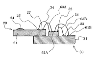
図1には、本発明の一実施形態に係るサーマルヘッドの概略断面図及び要部平面図を示す。図1(a)に示すように、サーマルヘッド10は、複数の薄膜層が形成されたヘッドチップ20と、このヘッドチップ20に重ねて接合された配線基板30とを有する。
Hereinafter, the present invention will be described in detail based on embodiments.
(One Embodiment of Thermal Head)
FIG. 1 shows a schematic cross-sectional view and a plan view of relevant parts of a thermal head according to an embodiment of the present invention. As shown in FIG. 1A, the
ヘッドチップ20は、セラミック基板21上に、各種薄膜層が形成されて構成される。まず、セラミック基板21上には、断熱層の機能を有するガラス系材質からなるグレース層22及びアンダーコート層23が形成されている。グレース層22は、セラミック基板21の一端から所定の距離をおいて断面が半円形状の凸条部22aを有し、この凸条部22aに対向する領域に、その長手方向に亘って所定間隔で間欠的に発熱体24が形成されている。また、各発熱体24の図中左右両側の端部に接触するように、アルミニウムなどの金属からなる電極25が形成されている。さらに、発熱体24の上部には、保護膜28が形成されている。
The
ここで、各発熱体24は、図1(b)に示すように一対の発熱体24a及び24bからなり、各発熱体24a及び24bのそれぞれの一端部には、電極25a及び25bが接続されている。電極25aは個別電極として機能し、端部には、例えば、金の薄膜層からなる端子部26に接続されている。また、電極25bは共通電極として機能し、セラミック基板21の発熱体24とは反対側の端部に設けられた共通電極27に接続されている。さらに、発熱体25a及び発熱体25bのそれぞれの他端部は、U字状の電極25cにより連結されている。
Here, each
一方、配線基板30は、ガラエポ基板などの基板31上に、ICチップ32と、外部端子33とが設けられている。ICチップ32は、上述した各発熱体24を選択的に発熱させるための駆動信号を出力するドライバとなる。ICチップ32は、発熱体24の所定の物理ブロック毎に設けられている。また、外部端子33は、各ICチップ32に外部信号を入力するためのものである。さらに、各ICチップ32は、上述した端子部26及び外部端子33とそれぞれボンディングワイヤ34により接続されている。なお、ICチップ32及びボンディングワイヤ34は、封止樹脂35によりモールドされている。
On the other hand, the
以上説明したサーマルヘッド10は、ヘッドチップ20と、このヘッドチップ20の支持基板となる配線基板30とを一部重ねて接合し、配線基板30上にICチップ32を搭載したものであるので、ヘッドチップ20の幅(図中左右方向)を著しく小さくでき、従って、基板工程でのヘッドチップ20の取り数が増大して生産性が向上するという利点を有する。また、ヘッドチップ20と配線基板30とを接合した状態で取り扱うことができるので、ICチップ32の搭載工程でのハンドリング性も低下しないという利点がある。この場合、後述するように、複数の配線基板30を切り取ることができる配線基板用プレート上に複数のヘッドチップ20を接合してICチップ32の搭載及びワイヤボンディングを行うようにすれば、ハンドリング性がさらに著しく向上するという効果を奏する。
(製造工程)
以下に、上述したサーマルヘッド10の製造工程の一例を示しながら、さらに詳細に説明する。
In the
(Manufacturing process)
Hereinafter, an example of the manufacturing process of the
基板工程の作業は基本的には従来技術と変わりがないので、詳細な説明は省略するが、ヘッドチップ20を小型化したので、一工程で製造できるヘッドチップ20の数が著しく増大し、大幅な生産性向上を図ることができる。
Since the substrate process is basically the same as the prior art, a detailed description is omitted. However, since the
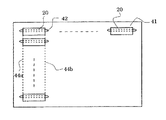
次に実装工程を図2及び図3を参照しながら説明する。図2は、実装工程の最初の段階を示す平面図であり、図3は、実装工程の概略工程を示す断面図である。 Next, the mounting process will be described with reference to FIGS. FIG. 2 is a plan view showing an initial stage of the mounting process, and FIG. 3 is a cross-sectional view showing a schematic process of the mounting process.
まず、配線基板用プレート41上に複数のヘッドチップ20を接合する。配線基板用プレート41の各ヘッドチップ20の接合位置に対応して長孔42が形成されている。長孔42は、長さがヘッドチップ20の長さより長く、幅はヘッドチップ20の配線基板30からの突出長さ(図1(a)中、Hで示す)より小さく形成されている。そして、ヘッドチップ20の発熱体側の端部が長孔42を幅方向に渡るように配置し、長孔42のヘッドチップ20の先端側の周縁部とヘッドチップ20とは接合しないようにする。すなわち、図3(a)においては、長孔42の左側の周縁部とヘッドチップ20との境界43aは接合されておらず、右側の周縁部とヘッドチップ20との境界43bのみが接合されている。従って、長孔42を利用して配線基板用プレート41を配線基板30に切断すると、長孔42の幅方向一方側の内周面42aが配線基板30の一端面を形成し、隣接する長孔42の他方側の内周面42bが配線基板30の他端面を形成する。
First, the plurality of
このように長孔42を形成して長孔42を渡るようにヘッドチップ20を配置することにより、ヘッドチップ20を安定して保持することができ、実装工程でのハンドリング性を大幅に向上することができると共に、配線基板30からヘッドチップ20の一端部が突出する構造を容易に形成することができる。
By thus forming the
ここで、ヘッドチップ20と配線基板用プレート41との接合手段は、特に制限されないが、例えば、粘着剤または接着剤をスクリーン印刷、ポッティング等により配線基板用プレート41の所定の位置に塗布した後、ヘッドチップ20を重ね合わせることにより行うことができる。また、両面テープを手作業で又は機械で貼着する方法を採用することもできる。好適には、固着力が直ぐに発生する粘着剤を用いるのが好ましい。
Here, the joining means of the
実装工程では、次ぎに、図3(b)に示すように、ヘッドチップ20に沿ってICチップ32を搭載する。
Next, in the mounting process, an
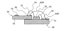
ここで、ICチップ32の搭載位置は、特に限定されないが、図4(a)に示すように、ヘッドチップ20から離して搭載してもよいし、図4(b)に示すように、ヘッドチップ20に密着して搭載してもよい。図4(a)の場合には、ICチップ32が搭載しやすく、図4(b)の場合には、上述したボンディングワイヤ34が短くてすむと共にサーマルヘッド全体が小型化できるという利点がある。
Here, the mounting position of the
次ぎに、図3(c)に示すように、ICチップ32と各端子とをボンディングワイヤ34により接続する。続いて、図3(d)に示すように、ICチップ32及びボンディングワイヤ34を封止樹脂35でモールドする。そして、最後に、図3(e)に示すように、配線基板用プレート41を所定の箇所(図2中、切断線44a及び44bで示す)で切断することにより、サーマルヘッド10とする。
Next, as shown in FIG. 3C, the
ここで、ワイヤボンディング、封止及び切断工程は従来から公知の技術を用いて行えばよい。例えば、切断方法としては、回転ブレードによる方法、押し切りによる方法、ダイセットによる打抜による方法、ルータによる切断、レーザ加工による切断、ウォータージェットによる切断などを用いることができる。 Here, the wire bonding, sealing, and cutting steps may be performed using a conventionally known technique. For example, as a cutting method, a method using a rotating blade, a method using push cutting, a method using punching with a die set, a cutting with a router, a cutting with laser processing, a cutting with a water jet, or the like can be used.
かかる実装工程は、以上説明したように、配線基板用プレート41上に、小型化したヘッドチップ20を接合した状態で行うことができるので、生産性が高く、大幅なコストダウンにつながる。
As described above, since the mounting process can be performed in a state where the
特に、ヘッドチップ20が配線基板30より突出して接合された構造を有するものでも、上述したような長孔42を用いることにより、ヘッドチップ20を安定して保持でき、且つ実装後の切断も容易となる。例えば、図1に示すヘッドチップ20の配線基板30からの突出量Hが、ヘッドチップ20の幅の20%以上、好ましくは50%以上となった場合には、上述したようにヘッドチップを長孔を渡した状態で保持することが必須となる。なお、突出量が70%を越えると、配線基板30との接合強度が不足するという問題がある。
In particular, even if the
また、このようにヘッドチップ20の端部が配線基板30から突出した構造を採ると、後述するようにヘッドチップ20の発熱体形成部の裏面側が直接放熱板と接触することになり、ヘッド特性が向上するという利点がある。
In addition, when the end portion of the
なお、上述した実装工程において、配線基板用プレート上へのヘッドチップの配列の方法も特に限定されず、また、長孔を有さないプレートを用いてもよい。 例えば、図5(a)に示すように、ヘッドチップ20を同一方向に向けてマトリックス状に配列してもよいし、図5(b)に示すように、一方向に並べた隙間に直交する方向に向けたヘッドチップ20を配列するようにしてもよい。 In the mounting process described above, the method of arranging the head chips on the wiring board plate is not particularly limited, and a plate having no long holes may be used. For example, as shown in FIG. 5A, the head chips 20 may be arranged in a matrix in the same direction, and as shown in FIG. 5B, the head chips 20 are orthogonal to gaps arranged in one direction. The head chips 20 oriented in the direction may be arranged.
また、長孔を有する場合には、長孔の形成方法も特に限定されず、例えば、図6に示すように、一つの長孔42A上に複数のヘッドチップ20を一列に配列できるようにしてもよい。この場合、ヘッドチップ20の配置の際の位置合わせが簡単になり、また、長さの異なるヘッドチップにも対応できるという利点がある。
(サーマルヘッドユニットの一実施形態)
以上説明したサーマルヘッド10は、アルミニウムなどの金属からなり放熱板の機能を有する支持体に保持してサーマルヘッドユニットとして用いられる。かかるサーマルヘッドユニットの一例を図7(a)に示す。
Further, in the case of having a long hole, the method of forming the long hole is not particularly limited. For example, as shown in FIG. 6, a plurality of
(One Embodiment of Thermal Head Unit)
The
図7(a)に示すように、支持体50は、ヘッドチップ20の配線基板30から突出して発熱体24を形成したヘッドチップ20の端部(以下、発熱体形成部という)の裏面側に密着してヘッドチップ支持部となる上段部51と、配線基板30の厚さより深く凹んだ段差部52とを有する。ヘッドチップ20の突出部である発熱体形成部と上段部51とは、接着層53で強固に固定され、段差部52の底部には接着剤層54が設けられている。このような構成により、支持体50と配線基板30とは接着剤層54で、支持体50とヘッドチップ20とは接着層53で強固に固定されている。
As shown in FIG. 7 (a), the
ここで、サーマルヘッド10は、段差部52の底部の接着剤層54が未硬化のうちにヘッドチップ20の発熱体形成部の裏面と上段部51との当接を基準にして接着層53により接合し、その後、接着剤層54の硬化処理(加熱、常温放置、紫外線照射など)を施すのが好ましい。これにより、配線基板30と支持体50との間の隙間の接着剤層54の存在により、ガラエポ基板などの配線基板30の反りは吸収され、ヘッドチップ20の発熱体形成部及び配線基板30は共に支持体50に密着固定される。
Here, the
また、接着剤層54に、未硬化時に比較的柔らかい接着剤を用いるのが好ましく、これにより、支持体50とヘッドチップ20との接合面を基準としたサーマルヘッドユニット構造が容易に実現できる。すなわち、段差部52の接着剤層54が未硬化の状態でヘッドチップ20の発熱体形成部と支持体50の上段部51とを接合すると共に、配線基板30を段差部52内の接着剤層54上に載せると、配線基板30と段差部52との隙間に充填されている接着剤層54が流動性のある又はペースト状の比較的柔らかい材質であると、この隙間が均一でなくてもヘッドチップ20と上段部51との接合面に影響を与えることがなく、ヘッドチップ20と上段部51との接合面が基準面となる。また、その後、接着剤層54を硬化するための処理を施しても、配線基板30の反りは接着剤層54に吸収され、ヘッドチップ20の発熱体形成部及び配線基板は支持体50に密着固定される。
In addition, it is preferable to use a relatively soft adhesive for the
このように、接着剤層54として用いる接着剤は、未硬化時に流動性があり、又はペースト状あるいは柔らかく粘着性があるという特性を有するものを用いるのが好ましい。また、接着剤層54は、接着層53より厚く設けるのが効果的である。
Thus, it is preferable to use the adhesive used as the
このようなヘッドチップ20の場合、配線基板30からの突出部である発熱体形成部が放熱体である支持体50から浮いた状態で接合されていると、発熱体の余分な熱を支持体50を介して逃がすことができないので、印字機能に悪影響があるが、このような悪影響は、上述したような支持構造とすることにより回避することができる。
In the case of such a
また、低コスト化を図ったサーマルヘッドでは、配線基板としてガラエポ基板を用いるが、この場合にも、上述した構造を採用することにより、熱膨張係数の違いによる接着境界部の応力が緩和され、硬化処理によるガラエポ基板の反りを吸収し、十分な接合強度を得ることができると共に、組立作業が困難となることを回避できる。 In addition, in the thermal head designed to reduce the cost, a glass epoxy substrate is used as a wiring substrate, but also in this case, by adopting the above-described structure, the stress at the bonding boundary due to the difference in thermal expansion coefficient is relieved, It is possible to absorb the warp of the glass epoxy substrate due to the curing process, obtain a sufficient bonding strength, and avoid the difficulty of assembling work.
ここで、上述した支持体50は、配線基板30の厚さをT1としたとき、深さをT2(T2>T1)とした段差部52を有していれば、特に限定されない。また、段差部52の形状は、接着剤層54の流出が防止できると共に、配線基板30に形成された回路と図示しない外部の駆動回路との接続配線とを安定に固定するため、凹部となっているのがよいが、例えば、図7(b)に示すように、断面L字状の段差部52Aであってもよい。
Here, the
また、図8に示すように、段差部52の底部に溝55を設けて接着剤層54の逃げ部を形成し、接着剤層54の支持体50の表面への流出をさらに防止するようにしてもよい。なお、溝55の数、形状は勿論限定されず、図8(a)に示すように1つ設けてもよいし、図8(b)に示すように2つ、又はそれ以上設けてもよく、さらに、断面矩形状の他、断面半円状の溝としてもよい。
Further, as shown in FIG. 8, a
ヘッドチップ20と支持体50の上段部51とを接合する接着層53は、発熱体形成部の余分な熱を逃がすためにしっかりと密着した状態を形成できるものであれば特に限定されず、両面テープ、粘着剤、又は接着剤を用いることができる。
The
また、段差部52の底部へ接着剤層54を設ける方法も特に限定されない。例えば、耐久性があり段差に対しても有効であるメタルマスクを用いた印刷が好適であるが、ディスペンサーを用いて注入する方法を採用することもできる。また、ガラエポ基板の反り、熱膨張係数の違いを吸収できるならば、シート状の粘着剤など別の材料を用いることもできる。
Further, the method for providing the
なお、サーマルヘッド10の支持体50への搭載方法は特に限定されないが、例えば、上述したような接着層53及び接着剤層54を用意した後、支持体50を治具にセットし、ヘッドチップ20の発熱体形成部を基準にしてサーマルヘッド10を外形合わせで支持体50に載せるようにする。また、支持体50及びサーマルヘッド10のそれぞれに合わせマークを付け、合わせマークを用いて認識・位置合わせをし、サーマルヘッドを支持体50に載せてもよい。そして、ヘッドチップ20の発熱体形成部及び配線基板30を同時に支持体50に押しつけ、しっかり密着させた後、接着剤層54を硬化させるために硬化処理を施す。また、他の方法として、ヘッドチップ20の発熱体形成部を基準にして支持体50にサーマルヘッド10を載せた後、配線基板30と支持体50の段差部52との間に接着剤を流し込み、その後、接着剤を硬化させる処理を施し、サーマルヘッド10と支持体50とを密着固定させることも可能である。
(サーマルヘッドの他の実施形態)
以上説明したサーマルヘッド10の利点について種々述べてきたが、ヘッドチップ20と配線基板30とを重ね合わせて接合し、配線基板30上にICチップ32を搭載したことにより、従来の構造と比較してICチップ32が相対的に低い位置に配置されているので、封止樹脂35の高さを低くすることができ、これにより、実際にサーマルプリンタ等に搭載したときに被印刷シートの搬送スペースを容易に確保できるという利点がある。すなわち、図9に示すように、発熱体24と対向して配置されるプラテンローラ57と、封止樹脂35との隙間が大きくなるので、被印刷シート58と封止樹脂35との干渉が避けられるという利点がある。
The method for mounting the
(Other embodiment of thermal head)
Although various advantages of the
また、このような効果を得るためには、上述したようにICチップ32の高さがヘッドチップ20の厚さより小さいものを用いるのが好ましいが、これに限定するものではなく、ICチップ32の高さをヘッドチップ20の厚さと同等程度としても同様な効果を奏する。
In order to obtain such an effect, it is preferable to use the
例えば、図10(a)に示すように、ヘッドチップ20の厚さと同等の高さを有するICチップ32Aを用いてもよく、また、図10(b)に示すように、ICチップ32の下に台部36を設けてICチップ32の高さをヘッドチップ20の厚さと同等としてもよいし、図10(c)に示すように、ヘッドチップ20の接合部が相対的に薄くなった段差部37を有する配線基板30Aを用いてICチップ32の高さとヘッドチップ20の厚さを同等になるようにしてもよい。このようにヘッドチップ20の厚さとICチップ32の高さを略同一とすることにより、ワイヤボンディングの作業がし易くなる。
For example, as shown in FIG. 10A, an
また、ヘッドチップ20と配線基板30との接合状態は、特に限定されない。図11(a)に示すように、上述した実施形態のようにヘッドチップ20を配線基板30から突出させる場合でも、発熱体が設けられた部分が全て突出してなくてもよく、又は、図11(b)に示すように、ヘッドチップ20の端面と配線基板30の端面とが重なっていてもよく、さらには、図11(c)に示すように、ヘッドチップ20の端面が配線基板30の端面より内側に入っていてもよい。これらの場合には、発熱体形成部の放熱の面では不利であるが、搭載が安定し、できるだけ小型化を図る上では有利である。また、図11(c)のようにヘッドチップ20の端面が配線基板30の端面より引っ込んでいると、製造時のヘッドチップ20の端部の接触破壊等を防止することができるという利点がある。
Further, the bonding state between the
さらに、これらの構造のサーマルヘッドを製造する場合にヘッドチップ20を搭載する配線基板用プレート41には、上述したような長孔42を形成してもしなくてもよいが、切断作業の容易化のためには長孔42を形成するのがよい。また、ヘッドチップ20を搭載する際の長孔42とヘッドチップ20の端部との位置関係も特に限定されず、図12(a)に示すように、ヘッドチップ20の端面が長孔42内に臨んでいてもよいし、図12(b)に示すように、ヘッドチップ20の端面と長孔42の内周面とが面一になっていてもよく、さらには、図12(c)に示すように、ヘッドチップ20の端面が長孔42から離れていてもよい。このような場合、ヘッドチップ20の搭載時の安定化を図ることができ、互いに傾きのない搭載が容易に実現できる。
(サーマルヘッドの配線構造)
上述したようなサーマルヘッドにおいて、ヘッドチップ20の小型化を図る場合、例えば、図1に示す共通電極27の幅を最小限に抑える必要がある。通常は、かかる共通電極27は、例えば、両端部で配線基板30上に設けられた共通電極用配線を介して外部端子に接続されて接地されるが、この場合、共通電極27が持つ電気抵抗によって、各発熱体24に流れる電流値にバラツキが生じる。すなわち、共通電極27の接地位置から離れた中央部に接続される発熱体24に流れる電流値は小さくなって発熱量が小さくなり、印字濃度ムラの原因となる。
Further, when manufacturing a thermal head having these structures, the
(Wiring structure of thermal head)
In the thermal head as described above, when the
そこで、本実施形態のサーマルヘッドでは、共通電極27の幅を最低限にしてセラミック基板21の幅の最小化を図ると共に、共通電極27と外部端子との接続を下記のように工夫することにより、各発熱体24間の印字濃度ムラの発生を防止する。
Therefore, in the thermal head of this embodiment, the width of the
図13(a)はヘッドチップ20の共通電極27と配線基板30の共通電極用配線との間の配線接続部の断面図であり、図13(b)は平面図である。
13A is a cross-sectional view of a wiring connection portion between the
これらの図面に示すように、配線基板30には共通電極用配線61が、各ICチップ32の間の領域まで設けられ、これら共通電極用配線61と、セラミック基板21の端部に設けられた共通電極27とは、それぞれボンディングワイヤ63により接続されている。また、各共通電極用配線61は、図示しない外部端子を介して接地される。すなわち、本実施形態では、共通電極27は、ICチップ32で規定される物理ブロック毎に配線基板30の共通電極用配線61に接続されている。
As shown in these drawings, the
したがって、共通電極27と配線基板30の共通電極用配線61との接続が、各ICチップ32で規定される物理ブロック毎に設けられているので、共通電極27の電気抵抗に基づく印字濃度ムラを低減することができる。すなわち、各発熱体に流れる電流値のばらつきを小さくし、各発熱体間での発熱量を均一にすることができる。
Accordingly, since the connection between the
なお、共通電極用配線61の数は、共通電極27の電気抵抗、印字の際に印加する電圧、ICチップ32に接続される発熱体の数、発熱体の電気抵抗等により決定すればよく、例えば、図14に示すように、2つのICチップ32毎に、又は3つ以上の複数のICチップ32毎に設けてもよい。
The number of
また、セラミック基板21の共通電極27と、配線基板30の共通電極用配線61の接続を、各物理ブロック内で複数設けたものである。すなわち、本実施形態では、さらに、図15に示すように、ICチップ32の略中央部の表面に共通電極用配線61Aと、それに対応する共通電極用配線61Bとを設け、共通電極27と共通電極用配線61A、さらに、共通電極用配線61Aと共通電極用配線61Bとをそれぞれボンディングワイヤ63A及び63Bで接続したものであり、他の構成は上述した実施形態と同様である。このように、共通電極27と、ICチップ32間の共通電極用配線との接続に加えて、ICチップ32の長手方向の略中間に共通電極27と共通電極用配線61Aとの接続を設けたことによって、各発熱体に流れる電流量の不均衡をさらに抑えることができ、印字の濃度ムラをさらに小さくすることができる。
Further, a plurality of connections between the
なお、各物理ブロック内における共通電極間の接続数、接続位置及び接続方法は特に限定されるものではなく、各物理ブロック毎に複数設けられていれば、同様の効果を奏する。
例えば、各物理ブロック内の接続をICチップ32の表面に設けた共通電極用配線61Aを介して行う代わりに、図16に示すように、ICチップ32の下側に設けた共通電極用配線61C及びボンディングワイヤ63Cを介して行ってもよい。この場合、ワイヤボンディングを容易に行うことができ、また、ボンディングワイヤの長さを短くすることができる。
In addition, the number of connections between common electrodes in each physical block, the connection position, and the connection method are not particularly limited, and the same effect can be obtained as long as a plurality of physical electrodes are provided for each physical block.
For example, instead of performing connection in each physical block via the
また、図17に示すように、ICチップ32の共通電極27とは反対側に設けられた共通電極用配線61Dと共通電極27とをICチップ32を跨ぐボンディングワイヤ63Dで接続するようにしてもよい。この場合には、ICチップ32上に共通電極用配線を設けるなどの加工が不要であるという利点がある。
In addition, as shown in FIG. 17, the
さらに、上述した実施形態では、共通電極と共通電極用配線との接続をワイヤボンディングにより行ったが、勿論これに限定されず、電気的に接続できるものであれば特に限定されない。 Further, in the above-described embodiment, the connection between the common electrode and the common electrode wiring is performed by wire bonding. However, the present invention is not limited to this, and is not particularly limited as long as it can be electrically connected.
図18(a),(b)は、他の実施形態に係るサーマルヘッドのヘッドチップと配線基板間の配線接続部の断面図及び平面図である。 18A and 18B are a cross-sectional view and a plan view of a wiring connection portion between a head chip and a wiring board of a thermal head according to another embodiment.
本実施形態は、ヘッドチップ20と配線基板30との高さを略同一とし、フリップチップ方式の半導体集積回路32Bをヘッドチップ20と配線基板30とを跨ぐように実装したものである。
In the present embodiment, the height of the
発熱体につながる個別電極25a上の端子部26及び外部端子33AとはICチップ32Bの下面のパッド71とバンプ72を介して接続されている。また、ICチップ32Bには、共通電極用配線のための互いに短絡されたパッド73が用意されており、これらパッド73は、それぞれバンプ74を介して共通電極27及び配線基板30上の共通電極用配線61Eに接続されている。このようにフリップチップ方式のICチップ32Bを用いることにより、ワイヤボンディングによる接続が必要なくなる。
The
勿論、フリップチップ方式のICチップの間で、共通電極と共通電極用配線との接続をワイヤボンディングにより行ってもよい。 Of course, the common electrode and the common electrode wiring may be connected by wire bonding between the flip-chip type IC chips.
以上説明したように、ヘッドチップの共通電極と外部端子との接続を、発熱体の配列方向の複数の箇所で行うことにより、サーマルヘッドの形状を小さく抑えたまま、印字ムラを低減することができるという効果を奏する。 As described above, by connecting the common electrode of the head chip and the external terminal at a plurality of locations in the arrangement direction of the heating elements, it is possible to reduce printing unevenness while keeping the shape of the thermal head small. There is an effect that can be done.
以上説明したように、本発明によれば、ヘッドチップの小型化を図ることができ、基板工程の生産性を向上させると共に、実装工程のハンドリング性を向上させ、大幅なコストダウンを図ることができるという効果を奏する。 As described above, according to the present invention, it is possible to reduce the size of the head chip, improve the productivity of the substrate process, improve the handleability of the mounting process, and greatly reduce the cost. There is an effect that can be done.
Claims (7)
Priority Applications (1)
| Application Number | Priority Date | Filing Date | Title |
|---|---|---|---|
| JP2006207374A JP4068647B2 (en) | 1998-08-11 | 2006-07-31 | Manufacturing method of thermal head |
Applications Claiming Priority (3)
| Application Number | Priority Date | Filing Date | Title |
|---|---|---|---|
| JP22710498 | 1998-08-11 | ||
| JP23460298 | 1998-08-20 | ||
| JP2006207374A JP4068647B2 (en) | 1998-08-11 | 2006-07-31 | Manufacturing method of thermal head |
Related Parent Applications (1)
| Application Number | Title | Priority Date | Filing Date |
|---|---|---|---|
| JP2000564820A Division JP3905311B2 (en) | 1998-08-11 | 1999-08-09 | Thermal head unit, thermal head manufacturing method, and thermal head unit manufacturing method |
Publications (2)
| Publication Number | Publication Date |
|---|---|
| JP2006289999A true JP2006289999A (en) | 2006-10-26 |
| JP4068647B2 JP4068647B2 (en) | 2008-03-26 |
Family
ID=37411069
Family Applications (1)
| Application Number | Title | Priority Date | Filing Date |
|---|---|---|---|
| JP2006207374A Expired - Lifetime JP4068647B2 (en) | 1998-08-11 | 2006-07-31 | Manufacturing method of thermal head |
Country Status (1)
| Country | Link |
|---|---|
| JP (1) | JP4068647B2 (en) |
Cited By (3)
| Publication number | Priority date | Publication date | Assignee | Title |
|---|---|---|---|---|
| JP2013202797A (en) * | 2012-03-27 | 2013-10-07 | Toshiba Hokuto Electronics Corp | Thermal print head |
| JP2016190462A (en) * | 2015-03-31 | 2016-11-10 | 東芝ホクト電子株式会社 | Thermal print head and thermal printer |
| JP2018058271A (en) * | 2016-10-05 | 2018-04-12 | 東芝ホクト電子株式会社 | Thermal print head and manufacturing method of the same |
-
2006
- 2006-07-31 JP JP2006207374A patent/JP4068647B2/en not_active Expired - Lifetime
Cited By (3)
| Publication number | Priority date | Publication date | Assignee | Title |
|---|---|---|---|---|
| JP2013202797A (en) * | 2012-03-27 | 2013-10-07 | Toshiba Hokuto Electronics Corp | Thermal print head |
| JP2016190462A (en) * | 2015-03-31 | 2016-11-10 | 東芝ホクト電子株式会社 | Thermal print head and thermal printer |
| JP2018058271A (en) * | 2016-10-05 | 2018-04-12 | 東芝ホクト電子株式会社 | Thermal print head and manufacturing method of the same |
Also Published As
| Publication number | Publication date |
|---|---|
| JP4068647B2 (en) | 2008-03-26 |
Similar Documents
| Publication | Publication Date | Title |
|---|---|---|
| KR100555341B1 (en) | Semiconductor device, method for manufacturing the same, circuit board, and flexible substrate | |
| US6853089B2 (en) | Semiconductor device and method of manufacturing the same | |
| US7521290B2 (en) | Method of manufacturing circuit device | |
| JP6076675B2 (en) | Semiconductor device | |
| JP2002324816A (en) | Semiconductor device and method for manufacturing the same | |
| JP2000150730A (en) | Semiconductor device and its manufacture | |
| CN110767553A (en) | Chip packaging method, chip and chip packaging assembly | |
| JP3905311B2 (en) | Thermal head unit, thermal head manufacturing method, and thermal head unit manufacturing method | |
| JP4549171B2 (en) | Hybrid integrated circuit device | |
| JP4068647B2 (en) | Manufacturing method of thermal head | |
| JP2009110980A (en) | Semiconductor device and method of manufacturing semiconductor device | |
| JP6255118B2 (en) | Semiconductor device | |
| KR100574813B1 (en) | Thermal head and thermal head unit | |
| JP3923661B2 (en) | Semiconductor device | |
| JP2714691B2 (en) | Manufacturing method of electronic component mounting board | |
| JP4572375B2 (en) | Manufacturing method of semiconductor device | |
| JP4036017B2 (en) | Electronic component mounting structure | |
| JP2001144247A (en) | Semiconductor device | |
| JP5741458B2 (en) | Mounting method of semiconductor package | |
| JPH06196516A (en) | Solder coating method, manufacture of semiconductor device, and squeegee | |
| JP2022019337A (en) | Liquid ejection head, and method for manufacturing the same | |
| JP3258298B2 (en) | Manufacturing method of heat sink for semiconductor device | |
| JP2004153004A (en) | Hybrid integrated circuit device and method for manufacturing the same | |
| JP2004039679A (en) | Circuit device | |
| JP2005057005A (en) | Method of manufacturing hybrid integrated circuit device |
Legal Events
| Date | Code | Title | Description |
|---|---|---|---|
| A621 | Written request for application examination |
Free format text: JAPANESE INTERMEDIATE CODE: A621 Effective date: 20060801 |
|
| A131 | Notification of reasons for refusal |
Free format text: JAPANESE INTERMEDIATE CODE: A131 Effective date: 20070109 |
|
| A521 | Written amendment |
Free format text: JAPANESE INTERMEDIATE CODE: A523 Effective date: 20070305 |
|
| A131 | Notification of reasons for refusal |
Free format text: JAPANESE INTERMEDIATE CODE: A131 Effective date: 20070724 |
|
| A521 | Written amendment |
Free format text: JAPANESE INTERMEDIATE CODE: A523 Effective date: 20070809 |
|
| TRDD | Decision of grant or rejection written | ||
| A01 | Written decision to grant a patent or to grant a registration (utility model) |
Free format text: JAPANESE INTERMEDIATE CODE: A01 Effective date: 20080108 |
|
| A61 | First payment of annual fees (during grant procedure) |
Free format text: JAPANESE INTERMEDIATE CODE: A61 Effective date: 20080110 |
|
| FPAY | Renewal fee payment (event date is renewal date of database) |
Free format text: PAYMENT UNTIL: 20110118 Year of fee payment: 3 |
|
| R150 | Certificate of patent or registration of utility model |
Ref document number: 4068647 Country of ref document: JP Free format text: JAPANESE INTERMEDIATE CODE: R150 Free format text: JAPANESE INTERMEDIATE CODE: R150 |
|
| RD01 | Notification of change of attorney |
Free format text: JAPANESE INTERMEDIATE CODE: A7421 Effective date: 20091108 |
|
| FPAY | Renewal fee payment (event date is renewal date of database) |
Free format text: PAYMENT UNTIL: 20110118 Year of fee payment: 3 |
|
| RD03 | Notification of appointment of power of attorney |
Free format text: JAPANESE INTERMEDIATE CODE: R3D03 |
|
| FPAY | Renewal fee payment (event date is renewal date of database) |
Free format text: PAYMENT UNTIL: 20110118 Year of fee payment: 3 |
|
| FPAY | Renewal fee payment (event date is renewal date of database) |
Free format text: PAYMENT UNTIL: 20120118 Year of fee payment: 4 |
|
| FPAY | Renewal fee payment (event date is renewal date of database) |
Free format text: PAYMENT UNTIL: 20130118 Year of fee payment: 5 |
|
| FPAY | Renewal fee payment (event date is renewal date of database) |
Free format text: PAYMENT UNTIL: 20140118 Year of fee payment: 6 |
|
| R250 | Receipt of annual fees |
Free format text: JAPANESE INTERMEDIATE CODE: R250 |
|
| R250 | Receipt of annual fees |
Free format text: JAPANESE INTERMEDIATE CODE: R250 |
|
| EXPY | Cancellation because of completion of term |