JP2006287935A - Multi-band mixer and quadrature signal generator for multi-mode radio receiver - Google Patents
Multi-band mixer and quadrature signal generator for multi-mode radio receiver Download PDFInfo
- Publication number
- JP2006287935A JP2006287935A JP2006096226A JP2006096226A JP2006287935A JP 2006287935 A JP2006287935 A JP 2006287935A JP 2006096226 A JP2006096226 A JP 2006096226A JP 2006096226 A JP2006096226 A JP 2006096226A JP 2006287935 A JP2006287935 A JP 2006287935A
- Authority
- JP
- Japan
- Prior art keywords
- signal
- quadrature
- communication
- mixer
- group
- Prior art date
- Legal status (The legal status is an assumption and is not a legal conclusion. Google has not performed a legal analysis and makes no representation as to the accuracy of the status listed.)
- Pending
Links
Images


Classifications
-
- H—ELECTRICITY
- H04—ELECTRIC COMMUNICATION TECHNIQUE
- H04B—TRANSMISSION
- H04B1/00—Details of transmission systems, not covered by a single one of groups H04B3/00 - H04B13/00; Details of transmission systems not characterised by the medium used for transmission
- H04B1/005—Details of transmission systems, not covered by a single one of groups H04B3/00 - H04B13/00; Details of transmission systems not characterised by the medium used for transmission adapting radio receivers, transmitters andtransceivers for operation on two or more bands, i.e. frequency ranges
- H04B1/0067—Details of transmission systems, not covered by a single one of groups H04B3/00 - H04B13/00; Details of transmission systems not characterised by the medium used for transmission adapting radio receivers, transmitters andtransceivers for operation on two or more bands, i.e. frequency ranges with one or more circuit blocks in common for different bands
- H04B1/0082—Details of transmission systems, not covered by a single one of groups H04B3/00 - H04B13/00; Details of transmission systems not characterised by the medium used for transmission adapting radio receivers, transmitters andtransceivers for operation on two or more bands, i.e. frequency ranges with one or more circuit blocks in common for different bands with a common local oscillator for more than one band
-
- H—ELECTRICITY
- H04—ELECTRIC COMMUNICATION TECHNIQUE
- H04B—TRANSMISSION
- H04B1/00—Details of transmission systems, not covered by a single one of groups H04B3/00 - H04B13/00; Details of transmission systems not characterised by the medium used for transmission
- H04B1/005—Details of transmission systems, not covered by a single one of groups H04B3/00 - H04B13/00; Details of transmission systems not characterised by the medium used for transmission adapting radio receivers, transmitters andtransceivers for operation on two or more bands, i.e. frequency ranges
- H04B1/0053—Details of transmission systems, not covered by a single one of groups H04B3/00 - H04B13/00; Details of transmission systems not characterised by the medium used for transmission adapting radio receivers, transmitters andtransceivers for operation on two or more bands, i.e. frequency ranges with common antenna for more than one band
- H04B1/0057—Details of transmission systems, not covered by a single one of groups H04B3/00 - H04B13/00; Details of transmission systems not characterised by the medium used for transmission adapting radio receivers, transmitters andtransceivers for operation on two or more bands, i.e. frequency ranges with common antenna for more than one band using diplexing or multiplexing filters for selecting the desired band
-
- H—ELECTRICITY
- H04—ELECTRIC COMMUNICATION TECHNIQUE
- H04B—TRANSMISSION
- H04B1/00—Details of transmission systems, not covered by a single one of groups H04B3/00 - H04B13/00; Details of transmission systems not characterised by the medium used for transmission
- H04B1/06—Receivers
- H04B1/16—Circuits
- H04B1/30—Circuits for homodyne or synchrodyne receivers
Abstract
Description
本発明は一般に、多数の帯域(マルチバンド)無線通信の装置とシステムとに関する。また特に、本発明は、無線通信装置のマルチバンド無線受信機に有用なマルチバンドミキサと直交位相信号発生器とに関する。 The present invention generally relates to multiple band (multiband) wireless communication devices and systems. More particularly, the present invention relates to a multiband mixer and a quadrature signal generator useful for a multiband radio receiver of a radio communication apparatus.
無線通信の分野が急速に発展し続けているため、使用するシステム及び周波数帯域の数が増大する結果となり、消費者への無線通信の配信が更に複雑になってきている。多くの場合、一つの特定の周波数帯域でサービスを提供しているネットワークオペレータは、無線サービスの顧客需要に対応すべく付加的な帯域のサービスを付加する必要がある。更に、通信事業者は、規格の異なる多数の無線通信システムを配置する必要がある。従って、セルラ無線電話機などの進歩した通信装置が遭遇しうる多様な無線通信システムで通信が可能となる多数の規格に準じた多数の周波数で、その装置が通信できなくてはならない。 As the field of wireless communication continues to develop rapidly, the result is an increase in the number of systems and frequency bands used, which further complicates the distribution of wireless communication to consumers. In many cases, network operators providing services in one specific frequency band need to add additional band services to meet customer demand for wireless services. Furthermore, it is necessary for a communication carrier to arrange a large number of wireless communication systems having different standards. Accordingly, the device must be able to communicate at a number of frequencies in accordance with a number of standards that allow communication with a variety of wireless communication systems that may be encountered by advanced communication devices such as cellular radiotelephones.
異なる無線通信システムが異なるキャリア周波数又は周波数帯域で動作し、同一の変調方式とベースバンド処理方式とを用いる場合は、デュアルバンド電話機又はマルチバンド電話機が特に望ましい。このような類似点を共有しているのは、例えば、周知のGSM(移動通信グローバルシステム、Global System for Mobile Communication)、パーソナル通信サービス(PCS)、デジタル通信システム(DCS)のシステムである。なおまた、今日のデジタル移動無線システムでは、RF(無線周波数)送信に2つ以上の周波数帯域を使用可能である。例として、欧州のGSMは2つの周波数帯域を用いており、これらはそれぞれ900MHz(GSM900)と1800MHz(GSM1800)とを中心とした25MHzの帯域幅であり、これらの周波数帯域の各々には、アップリンク(移動局から基地局への情報転送)の周波数帯域とダウンリンク(基地局から移動局への情報転送)の周波数帯域とがある。米国では、これら2つのGSM周波数帯域の中心はそれぞれ850MHzと1900MHzである。GSMでは更に、アップリンク帯域及びダウンリンク帯域の各々に、複数の周波数分割多重(FDM)サブバンドRFチャネルがあり、各帯域幅は200kHZである。従って、デュアルバンドのGSM移動電話は、GSM900帯域及びGSM1800帯域の両方を送受信できる。 Dual band telephones or multiband telephones are particularly desirable when different wireless communication systems operate at different carrier frequencies or frequency bands and use the same modulation scheme and baseband processing scheme. For example, well-known GSM (Global System for Mobile Communication), personal communication service (PCS), and digital communication system (DCS) systems share such similarities. Furthermore, in today's digital mobile radio systems, more than one frequency band can be used for RF (radio frequency) transmission. As an example, European GSM uses two frequency bands, each of which has a bandwidth of 25 MHz centered on 900 MHz (GSM900) and 1800 MHz (GSM1800), each of these frequency bands being up There is a frequency band of link (information transfer from the mobile station to the base station) and a frequency band of downlink (information transfer from the base station to the mobile station). In the United States, the centers of these two GSM frequency bands are 850 MHz and 1900 MHz, respectively. In GSM, there are a plurality of frequency division multiplexing (FDM) subband RF channels in each of the uplink band and the downlink band, and each bandwidth is 200 kHz. Therefore, a dual-band GSM mobile phone can transmit and receive both the GSM900 band and the GSM1800 band.
図1に模範的な先行技術のデュアルバンド無線受信機が示されており、基地局から送信されたRF信号群がアンテナ10で受信機に受信され、このアンテナ10がRF信号群を帯域スプリッタ30へと通し、この帯域スプリッタ30が受信した信号群を第1及び第2(又はそれ以上)の帯域に分ける。第1のバンドパスフィルタ(BPF)12aと第2のバンドパスフィルタ(BPF)12bとが、分けられた信号群をそれぞれ第1の帯域と第2の帯域とにフィルタリングし、これで2つの別個の通信帯域各々で受信機が受信できる。BPF12aとBPF12bとが出力したフィルタリング済みの信号群がそれぞれ直交位相復調(demod)ユニット32a〜32bに供給され、これらのユニットが、バンドパスでフィルタリングされた信号群を、更なる処理の為に同相ベースバンド信号(I信号)と直交位相ベースバンド信号(Q信号)とに変換する。直交位相復調ユニット32a〜bには、低雑音の増幅器(LNA)34a〜bと、分割器20a〜bと、ミキサ40a〜bとがある。分割器20a〜bが局部発振器(LO)36a〜bから受信した中間周波数信号を分割して、位相差が90°の中間の1/2信号と1/4信号を作る。生成されたLO信号群と増幅された受信信号群とを、第1のミキサ(ミキサ対40a、41a)と第2のミキサ(対40b、41b)とで混合して、Iベースバンド信号とQベースバンド信号を生成し、これらの信号をそれぞれ同相ローパスフィルタ42aと直交位相ローパスフィルタ42bでローパスフィルタリングする。次にフィルタリング済みのI信号及びQ信号はベースバンド処理回路44へと進み、このベースバンド処理回路44は、当該分野で周知のように、従来のベースバンド処理回路である。
FIG. 1 shows an exemplary prior art dual-band radio receiver, in which an RF signal group transmitted from a base station is received by an antenna 10 and the antenna 10 converts an RF signal group into a
図1の受信機を参照して分かるように、多くの受信機のハードウェアコンポーネント群を複製せずに多数の周波数の信号群を処理するマルチモード無線受信機を提供するのは困難である。先行技術では、受信機の設計に、バンドパスフィルタと、分割器と、局部発振器と、ミキサと、ローパスフィルタとを、提供される周波数帯域毎に別個に盛り込んでいる。
消費電力と受信機のハードウェアの複製を最小に抑えながらも多数の周波数帯域の信号を受信する能力のある無線通信装置の受信機が提供されることが望ましい。 It is desirable to provide a receiver for a wireless communication device capable of receiving signals in multiple frequency bands while minimizing power consumption and hardware duplication of the receiver.
本発明の一態様では、受信機が、複数の入力を持つマルチプレクサ回路を備え、この複数の入力の各入力が複数の信号経路の別個の信号経路に結合され、各信号経路が別個の周波数帯域の複数のRF信号の中から所定のRF信号を受信する。このマルチプレクサ回路が、複数の入力のうちの所定の入力で受信したRF信号をマルチプレクサ回路の所定の出力に選択的に送信する。受信機にはマルチプレクサ回路に結合されたミキサもあり、このミキサが、選択的に送信されたRF信号と所定の基準信号群とを受信し、所定の出力信号群を生成する為に、選択的に送信されたRF信号と基準信号とを組み合わせる。 In one aspect of the invention, a receiver comprises a multiplexer circuit having a plurality of inputs, each input of the plurality of inputs being coupled to a separate signal path of the plurality of signal paths, each signal path being a separate frequency band. A predetermined RF signal is received from the plurality of RF signals. The multiplexer circuit selectively transmits an RF signal received at a predetermined input of the plurality of inputs to a predetermined output of the multiplexer circuit. The receiver also includes a mixer coupled to a multiplexer circuit that receives the selectively transmitted RF signal and the predetermined reference signal group and selectively generates the predetermined output signal group. The RF signal transmitted to the reference signal is combined with the reference signal.
本発明の別の態様では、複数の周波数帯域の通信信号群を受信する通信装置が、所定の複数の周波数帯域の通信信号群を受信するアンテナ回路と、前記複数の周波数帯域のうちの第1の周波数帯域の通信信号群を受信する為にアンテナ回路に結合された第1の信号経路と、前記複数の周波数帯域のうちの第2の周波数帯域の通信信号群を受信する為にアンテナ回路に結合された第2の信号経路と、第1の信号経路と第2の信号経路とに結合された信号経路信号回線とを備え、第1の信号経路又は第2の信号経路のどちらかで検出された通信信号群が信号経路信号回線の所定の出力に転送される。通信装置には更に、所定の基準信号群を生成する信号発生器と、信号経路信号回線の出力に結合されたミキサとがあり、このミキサが、信号経路信号回線に転送された通信信号群を受信し、所定の出力通信信号群を生成するよう基準信号群と組み合わせる。
本発明の更なる別の態様では、複数の周波数帯域の通信信号群を受信する方法が、所定の複数の周波数帯域のうち所定の一つの周波数帯域の通信信号群を受信する工程と、この通信信号は所定の帯域幅を持ち、複数の周波数帯域のうちの第1の周波数帯域の通信信号群を第1の信号経路に結合する工程と、複数の周波数帯域のうちの第2の周波数帯域の通信信号群を第2の信号経路に結合する工程と、第1の信号経路又は第2の信号経路のうち一方のアサートされた通信信号群をミキサの第1の入力に結合する工程と、所定の局部発振器信号群をミキサの第2の入力に結合する工程と、を含む。本方法は、ミキサの出力を生成する為に、局部発振器信号群と前記アサートされた通信信号群とを第1の周波数帯域又は第2の周波数帯域のどちらかで混合する工程で締めくくられる。
In another aspect of the present invention, a communication device that receives communication signal groups in a plurality of frequency bands includes an antenna circuit that receives communication signal groups in a predetermined plurality of frequency bands, and a first of the plurality of frequency bands. A first signal path coupled to an antenna circuit for receiving a communication signal group in a frequency band of the second frequency band, and an antenna circuit for receiving a communication signal group in a second frequency band of the plurality of frequency bands. A second signal path coupled and a signal path signal line coupled to the first signal path and the second signal path, the detection being performed on either the first signal path or the second signal path; The transmitted communication signal group is transferred to a predetermined output of the signal path signal line. The communication device further includes a signal generator for generating a predetermined reference signal group and a mixer coupled to the output of the signal path signal line. The mixer is configured to convert the communication signal group transferred to the signal path signal line. Receive and combine with the reference signal group to generate a predetermined output communication signal group.
In still another aspect of the present invention, a method for receiving a communication signal group of a plurality of frequency bands includes a step of receiving a communication signal group of a predetermined one frequency band among a plurality of predetermined frequency bands, and the communication The signal has a predetermined bandwidth, the step of coupling the communication signal group of the first frequency band of the plurality of frequency bands to the first signal path, and the second frequency band of the plurality of frequency bands Coupling the communication signal group to the second signal path; coupling the asserted communication signal group of one of the first signal path or the second signal path to the first input of the mixer; Coupling the local oscillator signal group to a second input of the mixer. The method concludes with the step of mixing the local oscillator signal group and the asserted communication signal group in either the first frequency band or the second frequency band to produce the output of the mixer.
本発明は、マルチバンド受信機を提供するよう一つの高利得のマルチバンドミキサを備え、帯域選択のために直並列インタフェース(SPI)を選択可能な段を独自に構成することにより、電力削減とコスト削減がもたらされる。帯域ごとの個々のミキサをなくし、低雑音増幅器(LNA)入力段を不要にすることで、集積回路のダイ面積及び電流の消耗を実質的に低減させる。更に、直交位相信号発生器の各々に必要とされる入力バッファ及びバイアス回路が一つだけなので、ダイ面積及び電流の消耗を更に低減できる。
The present invention includes a single high-gain multi-band mixer to provide a multi-band receiver and uniquely configures a stage that can select a serial-parallel interface (SPI) for band selection, thereby reducing power consumption. Cost reduction is brought about. Eliminating individual mixers per band and eliminating the need for low noise amplifier (LNA) input stages substantially reduces integrated circuit die area and current consumption. Furthermore, since only one input buffer and bias circuit is required for each quadrature signal generator, die area and current consumption can be further reduced.
本発明は、以下の説明の好適な実施形態で記載され、本説明は、以下のとおりに、同じ数字が同一の又は同様な要素を表す図面に関する。
本発明の模範的な実施形態の以下の詳細な記述では、その実施形態の一部を成す添付の図面について述べられており、これらの図面では、本発明を実践し得る特殊な模範的実施形態実例として示されている。
The present invention is described in preferred embodiments in the following description, which relates to the drawings in which like numerals represent the same or similar elements as follows:
In the following detailed description of exemplary embodiments of the invention, reference is made to the accompanying drawings that form a part hereof, and in these drawings are shown specific exemplary embodiments in which the invention may be practiced. It is shown as an example.
本発明に係るマルチバンド高利得ミキサと直交位相信号発生器とによって、受信機システムが多大なハードウェアの複製を必要とせずに多数の周波数帯域の信号を受信することが可能になる。この成果を達成する為に、好適な実施形態の単一のミキサが、DCS、PCS、UMTS(Universal Mobile Telecommunication System))(UMTSの日本の800MHz帯域やUMTSの米国の800MHz帯域などを含む)のいずれかを、増幅せず直接的に受信でき、RF入力を単一の局部発振器信号と混合してマルチモードの受信機から共通のIF出力を生成できる。先行技術に見られる全ての低雑音増幅器(LNA)と複製ミキサとをなくすことにより、ダイ面積と電流の消耗とが著しく低減された無線受信機が得られる。 The multiband high gain mixer and quadrature signal generator according to the present invention allows the receiver system to receive signals in multiple frequency bands without requiring extensive hardware duplication. To achieve this result, a single mixer of the preferred embodiment includes DCS, PCS, UMTS (Universal Mobile Telecommunication System) (including UMTS's 800 MHz band in Japan and UMTS's 800 MHz band in the US). Either can be received directly without amplification, and the RF input can be mixed with a single local oscillator signal to produce a common IF output from a multimode receiver. By eliminating all the low noise amplifiers (LNAs) and replica mixers found in the prior art, a radio receiver with significantly reduced die area and current consumption is obtained.
ここで図2を参照すると、描写されているのは、本発明が組み込まれた、セルラ無線電話機などの無線通信装置100のブロック図である。好適な実施形態では、フレーム生成ASIC101とマイクロプロセッサ103とを組み合わせて、セルラ通信システムでの動作に必要な通信プロトコルを生成する。マイクロプロセッサ103が使用するメモリ104にはRAM105とFLASH107とROM109とがあり、これらは好ましくは1つのパッケージ111に統合されており、プロトコルを生成する為に必要な工程を実行し、無線通信装置100の他の機能を行い、これらの機能は例えば、ディスプレイ113への書き込みや、キーパッド115からの情報の受け取りや、コネクタ116を介した入力/出力(I/O)情報の受け取りや、周波数シンセサイザ125の制御や、本発明の方法に従う信号の増幅に必要な工程を行うことなどである。マイクロプロセッサ103は更に、マイクロホン117から入り音声回路119により変形された音声を処理してスピーカ121に送る。無線通信装置100には任意選択でメッセージ受信機及び記憶装置130があってもよく、これには例えばデジタル留守電装置やページング受信機として使用されるデジタル信号処理手段などがある。
Referring now to FIG. 2, depicted is a block diagram of a
無線通信装置100の無線周波数の信号をトランシーバ122が処理する。中でも特に、送信機123が周波数シンセサイザ125により作られたキャリア周波数を用いアンテナ129を介して送信を行う。アンテナ129が受信した情報信号は、受信機127に入り、周波数シンセサイザ125によるキャリア周波数を用い復調される。その結果として生じたベースバンド信号が、当該分野で周知のように、ベースバンド処理の為にマイクロプロセッサ103へと送出される。
The
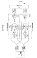
図3が示すのは、本発明の好適な実施形態に従って、マルチバンド受信機能を無線通信装置100に提供するよう動作可能な受信機127のブロック図である。この実施形態では、無線通信装置100により提供されたデュアルバンドの受信信号群を混合するのは、単一のマルチバンド高利得ミキサ(Iチャネルのミキサコア要素240とQチャネルのミキサコア要素241と多入力の相互コンダクタンス(gm)段235とが含まれる)である。基地局又は他のRF送信機から送信されたRF信号を受信する為に受信機127がアンテナ129に結合されている。この受信した信号を、アンテナ129に結合された帯域スプリッタ(band splitter)230が第1及び第2(又はそれ以上)の帯域又は経路に分け、帯域スプリッタ230に結合されたバンドパスフィルタ(BPF)212a及び212bへの出力とする。バンドスプリッタ230は、選択した周波数帯域のみがBPF212へと進むよう、マイクロプロセッサ103により選択可能である。他の実施形態では、所望の周波数帯域の選択にソフトウェア又はフィルタリングの構成要素が使用できる。動作周波数帯域を選択する信号がマイクロプロセッサ103又はシンセサイザ125から出力され、例えば、無線通信デバイス100が現在受信中の周波数帯域を示す。この帯域選択は、当該加入者によって確認されてもよいし、受信した通信信号と共に供給された制御信号によって確認されてもよい。
FIG. 3 shows a block diagram of a
分けられた信号群を、それぞれ第1の周波数帯域と第2の周波数帯域に第1のバンドパスフィルタ(BPF)212aと第2のバンドパスフィルタ(BPF)212bとがフィルタリングするので、受信機127が所望の受信する通信帯域を選択できる。例えば、バンドパスフィルタ群212を、UMTS2100帯域及びDCS1800帯域の各々の帯域幅をフィルタリングするよう構成してもよい。バンドパスフィルタ212は周波数(帯域)に特定のものであり、受信機の直線性が相対的に高い場合は省いてもよい。代案として、高品質のバンドパスフィルタが用いられている場合は帯域スプリッタ230を省いてもよい。たいていの場合、消費電力を最小にするにはバンドパスフィルタ212が望ましい。更なる代案としては、帯域スプリッタとバンドパスフィルタを、一つの入力と多数の出力(帯域ごとに1出力)とを有した単一のマルチバンドフィルタ(図示せず)と取り替えてもよい。
Since the first band pass filter (BPF) 212a and the second band pass filter (BPF) 212b filter the divided signal groups into the first frequency band and the second frequency band, respectively, the
バンドパスフィルタ212aとバンドパスフィルタ212bとにより出力されたフィルタリング済みの信号群が、無線通信システムの所望の動作周波数帯域を選択する為に、マルチ入力の直並列インタフェース(SPI)を選択可能なgm段235に供給される。gm段235がBPF212群からフィルタリング済みの帯域幅の各々を入力として受信し、SPI制御部250からの適用された制御信号に応えて、帯域経路(BPF群212からの2つの出力のうち一方)をミキサコア240とミキサコア241への出力用に選択する。RF信号のアサートされた帯域経路が選択されてミキシング回路への出力となり、信号のアサートされていない帯域経路は遮断され受信機127の電流を消耗しない。
Gm capable of selecting a multi-input serial / parallel interface (SPI) for selecting a desired operating frequency band of the wireless communication system based on filtered signal groups output by the band-pass filter 212a and the band-
選択した周波数帯域の受信した信号群の同相成分(I信号)と直交成分(Q信号)とを、直交位相復調ユニット248が生成する。直交位相復調ユニット248に含まれるのは、単一のマルチバンド高利得ミキサ243(ミキサコア要素240、ミキサコア要素241、gm段235)であり、このミキサ243は、スイッチ235から受信した信号群と、直交位相信号発生器245により出力された直交位相信号群とを混合する。直交位相信号発生器245には電圧制御発振器(VCO)236があり、このVCO236はこれに結合されたバッファ237の入力に局部発振器信号(LO)を生成する。VCO236の帯域幅は相対的に大きく、受信機が受信できる周波数帯域の全てを十分包含するか、代案としてVCO236が周波数の多数の発振を切替可能であってもよい。増幅された発振器信号がバッファ237から出力され、同相成分(I)と直交成分(Q)とに分離される(即ち、信号群の位相が90°だけ離される)よう、バッファ237に結合されたハイバンド直交位相発生器238及びローバンド直交位相発生器239の各々へと入力される。直交位相生成器238は1/2直交位相生成器であり、相対的に高い帯域、例えば、PCS1900、DCS1800、UMTS2100向けである。直交位相生成器239は1/4直交位相生成器であり、相対的に低い帯域、例えば、GSMの800MHz、900MHz、日本及び米国のW−CDMAの800MHzの直交位相信号群を生成する。従って、直交位相生成器238と直交位相生成器239とが、バッファ237から受信した中間周波数LO信号を、受信した帯域に依存して、半分に分割(1/2直交位相生成)又は四半分に分割(1/4直交位相生成)し、それによってLO信号群が、それぞれ半分又は四半分の周波数となり、直交位相信号発生器245の出力の(IとQとの)位相差が90°となる。直交位相生成器238と直交位相生成器239とが同一の入力バッファを利用し同一のバイアス回路を共有するので、集積回路のダイ面積が低減される。
The
代わりの方法では、直交位相信号発生器238と直交位相信号発生器239を、VCO236により生成された発振信号から直交位相の局部発振器(LO)信号群を生成する周波数分割器と取り替えてもよい。信号の周波数を2で分割することで、2つの直交位相信号を生成することが可能になる。周波数2fの差分信号が2で分割され、各信号の立ち上がりエッジが分割された信号のエッジを制御する。2fの1/2波長が周波数fの波長の1/4に等しいので、その結果として生じた信号は直交位相信号である。周波数分割器を用いるには、VCO236が所望の周波数の適切な倍数で動作する必要がある。例えば、1つ又は2つの周波数で動作する際には、周波数分割器はそれぞれ2で又は2と4で分割する。
Alternatively, quadrature signal generator 238 and quadrature signal generator 239 may be replaced with a frequency divider that generates quadrature local oscillator (LO) signals from the oscillation signal generated by
直交位相信号発生器245からの局部発振器I信号及び局部発振器Q信号を、単一のミキサ243(ミキサコア240と、ミキサコア241と、gm段235とから成る)が、ミキサコア240及びミキサコア241のLO入力で受信し、更に、RF信号群をgm段235からの入力で受信し、このgm段235は出力に際して電圧を電流に変換する。ミキサコア240とミキサコア241とが、受信したRF入力を、それぞれ対応したI信号群及びQ信号群と混合して、同相成分を持つIF出力と直交成分を持つIF出力とを生成する。もちろん、直交位相復調を用いて単一のRF信号を復調する為にもミキサコア240とミキサコア241は必要なので、単一のミキサ243の重要な要素である。他の復調技術を利用する代替の好適な実施形態では、例えば、同相成分信号のみを用いる場合に、任意のRF信号を復調する必要があるのはミキサコアの一方(即ち、ミキサコア240又はミキサコア241のどちらか)だけである。ミキサ243からのI信号出力とQ信号出力が、それぞれ同相ローパスフィルタ242aと直交位相ローパスフィルタ242bに結合される。ローパスフィルタ242aとローパスフィルタ242bは好ましくは、異なる帯域幅を持つ二つ以上の帯域に受信機127が対応できるようプログラム可能な帯域幅を持つ。次にフィルタリング済みのI信号及びQ信号は、当該分野で周知のように、ベースバンド処理の為にベースバンド処理回路へと進む。
The local oscillator I signal and the local oscillator Q signal from the
ここで図4を参照すると、本発明の好適な実施形態に係るgm段235及びミキサ243の回路図が示されている。ある実施形態で実施される際には、受信機127がトリプルバンド受信機であり、3つの別個の周波数帯域、例えば、UMTS、PCS、日本及び米国のWCDMA800を支持できる。これらの3つの入力帯域からのRF入力信号の各々が、図4の実施形態では、差動入力のRF入力1、RF入力2、RF入力3として示されている。RF入力1、2、3は、SPIを選択可能なgm段235への入力として、それぞれ402、404、406で結合されている。各gm段402、404、406には、それぞれ、n型の金属酸化物半導体(MOS)トランジスタ対402a〜b、404a〜b、406a〜bがある。トランジスタ対402a〜b、404a〜b、406a〜bのゲートに帯域の異なるRF信号群が入力され、トランジスタ対402a〜b、404a〜b、406a〜bの出力群が連結され、I及びQのチャネルミキサコア240及び241へと進む。よってgm段とミキサコア群とが同一の電流を共有する。トランジスタの対402a〜b、404a〜b、406a〜bのソースが、それぞれ、差動インダクタ420a、420b、420cに結合されている。差動インダクタの中心は接地されている。性能改善の為に、gm段235とマルチバンド高利得ミキサ243と直交位相信号発生器245の、MOSデバイスに関しては本体とソースとが連結され、デバイスの電流の消耗を増加させずに入力基準3次インターセプトポイント(IIP3)を改善する。gm段402がRF入力1を受信したときは、他のgm段404とgm段406とがSPI制御部250により遮断される。代案として、gm段406を省いて受信機127の動作に影響を及ぼさずに受信機127をデュアルバンド受信機として実施してもよい。gm段402〜406の出力群がミキサ243の差動入力群と並列に結合されている。g−m段235は、SPI制御部250の制御により、ミキサ243へのRF入力群のマルチプレクサの入力として一緒に動作する。gmの段の出力群が並列に連結されておりミキサ及び負荷が一つだけになるので、ミキサセルのダイ面積と負荷とが低減される。
Referring now to FIG. 4, a circuit diagram of the
ミキサ243の各ミキサコア240、241が4個のn型のバイポーラトランジスタ(それぞれトランジスタの対408a〜bとトランジスタの対410a〜bと確認される)を用いて相互に接続され、周知の「ギルバートセル」ミキサ構成を形成している。ギルバートセルは無線電話機及び他のRF応用例に用いられるミキサ構成であり、その設計及び動作は当業者に周知なので、詳細には説明しない。ミキサコア240が、ミキサ240と負荷抵抗器412との間のノードと、ミキサ240と負荷抵抗器414との間のノードで生成するのは、gm段235からの選択したRF入力と直交位相生成器245から受信した差動同相LO信号群(lo_I、lo_Ix)とを混合することによりもたらされる差動同相(I)信号出力(I_out、Ix_out)である。ミキサコア241が、ミキサ241と負荷抵抗器416との間のノードと、ミキサ241と負荷抵抗器418との間のノードで生成するのは、gm段235からの選択したRF入力と直交位相生成器245から受信した差動直交位相LO信号群(lo_Q、lo_Qx)とを混合することによりもたらされる、差動直交位相(Q)信号出力(Q_out、Qx_out)である。図4に示された回路では、インダクタ420a〜cの中心に接地接続(gnd_mix)があり、負荷抵抗器412〜418の終端にチップ電源(vcc_mix)がある。当業者には明らかなように、受信した周波数帯域を選択するとき、ミキサコアのバイアス電流と、帯域選択段と、直交位相信号発生器とが、トランシーバの直線性と、ゲインと、雑音指数とを最適化するようSPIを選択可能である。
Each
本発明の好適な実施形態がデュアルバンド(図3)受信機とトリプルバンド(図4)受信機として記載されたが、当然のことながら、本発明はこれらの実施形態に制限されておらず、記載した好適な実施形態を修正して、他の通信システムの信号を受信するようgm段235の入力に付加的なRF経路を備え、クワッドバンド又はマルチバンド(4つより多くの帯域)の受信機としても実施可能である。これらの好適な実施形態は、差動RF入力に付加的なRF入力の各々を送信することにより実施され、付加的なgm段の出力がミキサ243の入力でgm段402〜406に並列して接続されている。例えば、無線通信装置100を、gm段235に向かう第4のRF経路でGSMの900メガヘルツの信号群を受信するよう適応させられる。よって、もちろん、本実施形態では3つの差動RF入力が示されているが、所望の受信する周波数帯域数に依存して付加的な段を必要に応じて使用可能である。
Although preferred embodiments of the present invention have been described as dual band (FIG. 3) and triple band (FIG. 4) receivers, it should be understood that the present invention is not limited to these embodiments, The preferred embodiment described is modified to provide an additional RF path at the input of the
示してきた通り、本発明は、マルチバンド受信機を提供するよう一つの高利得のマルチバンドミキサを備え帯域選択の為にSPIを選択可能な段を独自に構成することにより、電力とコストについての大きな利点がもたらされる。帯域ごとの個々のミキサをなくしLNA入力段を不要にすることで、集積回路のダイ面積及び電流の消耗を実質的に低減させる。更に、直交位相信号発生器の各々に必要とされる入力バッファ及びバイアス回路が一つだけなので、ダイ面積及び電流の消耗を更に低減できる。 As has been shown, the present invention provides a multi-band receiver with a single high-gain multi-band mixer that uniquely configures an SPI-selectable stage for band selection, thereby reducing power and cost. The great benefits of Eliminating individual mixers per band and eliminating the need for LNA input stages substantially reduces the die area and current consumption of the integrated circuit. Furthermore, since only one input buffer and bias circuit is required for each quadrature signal generator, die area and current consumption can be further reduced.
本発明が図面の上記の記述により記載され図示されたが、この記述が単に例としてなされたものであり、本発明の真の精神及び範囲から逸脱することなく非常に多くの変更及び修正が当業者には可能であるということが分かる。例えば、特殊な受信帯域を持つ特殊な無線電話システムが記載された。しかし、他の規格や周波数帯域を用いた他のシステムを本発明により検討できる。なおまた、本発明は持ち運びできるセルラ無線電話機の特定の応用例を見出したが、本発明は、ページャ、電子手帳、コンピュータ、ゲームなど、任意の無線通信装置に適用可能である。本発明を好適な実施形態に関して特に示され記載したが、当業者には明らかなように、本発明のシステム精神及び範囲から逸脱することなく形式及び詳細に関し種々の変更が本発明になされてよい。記載した実施形態に対し、あらゆる変形、修正、付加、改善が可能であり、以下の請求項に詳述した本発明の範囲内にある。 While the invention has been described and illustrated by the foregoing description of the drawings, this description has been made by way of example only and numerous changes and modifications may be made without departing from the true spirit and scope of the invention. The trader knows that it is possible. For example, a special wireless telephone system having a special reception band has been described. However, other systems using other standards and frequency bands can be considered by the present invention. Although the present invention has found a specific application example of a portable cellular radio telephone, the present invention can be applied to any wireless communication device such as a pager, an electronic notebook, a computer, and a game. Although the invention has been particularly shown and described with respect to preferred embodiments, it will be apparent to those skilled in the art that various changes in form and detail may be made to the invention without departing from the spirit and scope of the invention. . All variations, modifications, additions and improvements to the described embodiments are possible and are within the scope of the invention as detailed in the following claims.
100…無線通信装置。125…周波数シンセサイザ。127…受信機システム。129…アンテナ。212…バンドパスフィルタ。230…帯域スプリッタ。235、240、241…ミキサ。236…電圧制御発振器(VCO)。237…バッファ。238、239…直交位相信号発生器。242…低域フィルタ。 100: A wireless communication device. 125: Frequency synthesizer. 127: Receiver system. 129. Antenna. 212: Band pass filter. 230: Band splitter. 235, 240, 241, ... mixers. 236: Voltage controlled oscillator (VCO). 237 ... Buffer. 238, 239: Quadrature signal generator. 242: Low-pass filter.
Claims (20)
前記選択回路に結合され、前記選択的に送信されたRF信号と基準信号群とを受信して組み合わせることによって出力信号群を生成するミキサコアと、
を備える受信機。 It has a plurality of inputs, each input of the plurality of inputs is coupled to each signal path of a plurality of signal paths, and each signal path receives a predetermined RF signal from a plurality of RF signals in the respective frequency bands. The selection circuit for selectively transmitting an RF signal received at a predetermined input of the plurality of inputs to an output of the selection circuit;
A mixer core coupled to the selection circuit for generating an output signal group by receiving and combining the selectively transmitted RF signal and a reference signal group;
Receiver with.
複数の周波数帯域の通信信号群を受信するアンテナ回路と、
前記複数の周波数帯域のうちの第1の周波数帯域の通信信号群を受信するために前記アンテナ回路に結合された第1の信号経路と、
前記複数の周波数帯域のうちの第2の周波数帯域の通信信号群を受信するために前記アンテナ回路に結合された第2の信号経路と、
前記第1の信号経路と前記第2の信号経路とに結合されて、前記第1の信号経路又は前記第2の信号経路のどちらかで検出された通信信号群を信号経路選択回路の出力に転送する前記信号経路選択回路と、
基準信号群を生成する信号発生器と、
前記信号経路選択回路に転送された通信信号群を受信し、前記基準信号と組み合わせて出力通信信号群を生成するための、前記信号経路選択回路の出力に結合されたミキサコアと、
を備える通信装置。 A communication device that receives a communication signal group of a plurality of frequency bands, the communication device,
An antenna circuit for receiving communication signal groups in a plurality of frequency bands;
A first signal path coupled to the antenna circuit for receiving a communication signal group in a first frequency band of the plurality of frequency bands;
A second signal path coupled to the antenna circuit for receiving a communication signal group in a second frequency band of the plurality of frequency bands;
The communication signal group detected by either the first signal path or the second signal path is coupled to the first signal path and the second signal path as an output of the signal path selection circuit. The signal path selection circuit to transfer;
A signal generator for generating a reference signal group;
A mixer core coupled to the output of the signal path selection circuit for receiving the communication signal group transferred to the signal path selection circuit and generating an output communication signal group in combination with the reference signal;
A communication device comprising:
複数の周波数帯域のうちの一つの周波数帯域の、帯域幅を有する通信信号群を受信する工程と、
前記複数の周波数帯域のうちの第1の周波数帯域の通信信号群を第1の信号経路に結合する工程と、
前記複数の周波数帯域のうちの第2の周波数帯域の通信信号群を第2の信号経路に結合する工程と、
前記第1の信号経路又は前記第2の信号経路のうち一方のアサートされた通信信号群をミキサの第1の入力に結合する工程と、
局部発振器信号群を前記ミキサの第2の入力に結合する工程と、
前記ミキサの出力を生成するために、前記局部発振器信号と前記アサートされた通信信号とを、前記第1の周波数帯域又は前記第2の周波数帯域のどちらかで混合する工程と、
を含む方法。 A method for receiving communication signal groups in a plurality of frequency bands, the method comprising:
Receiving a communication signal group having a bandwidth of one of a plurality of frequency bands;
Coupling a communication signal group of a first frequency band of the plurality of frequency bands to a first signal path;
Coupling a communication signal group in a second frequency band of the plurality of frequency bands to a second signal path;
Coupling one asserted group of communication signals of the first signal path or the second signal path to a first input of a mixer;
Coupling a local oscillator signal group to a second input of the mixer;
Mixing the local oscillator signal and the asserted communication signal in either the first frequency band or the second frequency band to generate the output of the mixer;
Including methods.
第1の発振器信号を生成する工程と、
同相発振器信号と直交位相発振器信号とを生成するために前記第1の発振器信号を分周する工程とを更に備え、前記局部発振器信号が前記同相発振器信号と前記直交位相発振器信号を含んでいる、方法。 The method according to claim 16, comprising:
Generating a first oscillator signal;
Dividing the first oscillator signal to generate an in-phase oscillator signal and a quadrature oscillator signal, wherein the local oscillator signal includes the in-phase oscillator signal and the quadrature oscillator signal; Method.
Applications Claiming Priority (1)
| Application Number | Priority Date | Filing Date | Title |
|---|---|---|---|
| US11/098,490 US7392026B2 (en) | 2005-04-04 | 2005-04-04 | Multi-band mixer and quadrature signal generator for a multi-mode radio receiver |
Related Child Applications (1)
| Application Number | Title | Priority Date | Filing Date |
|---|---|---|---|
| JP2012106291A Division JP2012165461A (en) | 2005-04-04 | 2012-05-07 | Multi-band mixer and quadrature signal generator for multi-mode radio receiver |
Publications (2)
| Publication Number | Publication Date |
|---|---|
| JP2006287935A true JP2006287935A (en) | 2006-10-19 |
| JP2006287935A5 JP2006287935A5 (en) | 2009-05-07 |
Family
ID=37071219
Family Applications (3)
| Application Number | Title | Priority Date | Filing Date |
|---|---|---|---|
| JP2006096226A Pending JP2006287935A (en) | 2005-04-04 | 2006-03-31 | Multi-band mixer and quadrature signal generator for multi-mode radio receiver |
| JP2012106291A Pending JP2012165461A (en) | 2005-04-04 | 2012-05-07 | Multi-band mixer and quadrature signal generator for multi-mode radio receiver |
| JP2015000471A Pending JP2015092738A (en) | 2005-04-04 | 2015-01-05 | Multi-band mixer and quadrature signal generator for multi-mode radio receiver |
Family Applications After (2)
| Application Number | Title | Priority Date | Filing Date |
|---|---|---|---|
| JP2012106291A Pending JP2012165461A (en) | 2005-04-04 | 2012-05-07 | Multi-band mixer and quadrature signal generator for multi-mode radio receiver |
| JP2015000471A Pending JP2015092738A (en) | 2005-04-04 | 2015-01-05 | Multi-band mixer and quadrature signal generator for multi-mode radio receiver |
Country Status (2)
| Country | Link |
|---|---|
| US (1) | US7392026B2 (en) |
| JP (3) | JP2006287935A (en) |
Cited By (1)
| Publication number | Priority date | Publication date | Assignee | Title |
|---|---|---|---|---|
| WO2019003419A1 (en) * | 2017-06-30 | 2019-01-03 | 三菱電機株式会社 | Receiver |
Families Citing this family (30)
| Publication number | Priority date | Publication date | Assignee | Title |
|---|---|---|---|---|
| US7366485B2 (en) * | 2004-03-04 | 2008-04-29 | Matsushita Electric Industrial Co., Ltd. | Multimode wireless transmitter and a portable wireless device using the same |
| US20070058584A1 (en) * | 2005-09-12 | 2007-03-15 | Ilan Sutskover | Techniques to transmit and duplex with channel knowledge at a base station |
| US7904036B2 (en) * | 2005-12-02 | 2011-03-08 | Telefonaktiebolaget Lm Ericsson (Publ) | Modulation method and apparatus |
| KR100646314B1 (en) * | 2005-12-16 | 2006-11-23 | 삼성전자주식회사 | Multi-input multi-frequency synthesizing apparatus and method for multi-band rf receiver |
| US8064835B2 (en) * | 2006-01-11 | 2011-11-22 | Quantenna Communications, Inc. | Antenna assignment system and method |
| US8091012B2 (en) * | 2006-05-04 | 2012-01-03 | Quantenna Communications Inc. | System and method for decreasing decoder complexity |
| TWI411255B (en) * | 2006-05-04 | 2013-10-01 | Quantenna Communications Inc | Multiple antenna receiver system and method |
| US7693544B2 (en) * | 2006-06-29 | 2010-04-06 | Intel Corporation | System, method and device of receiving signals of a plurality of communication services |
| US8063839B2 (en) * | 2006-10-17 | 2011-11-22 | Quantenna Communications, Inc. | Tunable antenna system |
| US7756504B2 (en) | 2007-06-29 | 2010-07-13 | Silicon Laboratories Inc. | Rotating harmonic rejection mixer |
| US8503962B2 (en) * | 2007-06-29 | 2013-08-06 | Silicon Laboratories Inc. | Implementing a rotating harmonic rejection mixer (RHRM) for a TV tuner in an integrated circuit |
| US8538366B2 (en) | 2007-06-29 | 2013-09-17 | Silicon Laboratories Inc | Rotating harmonic rejection mixer |
| US8260244B2 (en) * | 2007-06-29 | 2012-09-04 | Silicon Laboratories Inc. | Rotating harmonic rejection mixer |
| US7860480B2 (en) * | 2007-06-29 | 2010-12-28 | Silicon Laboratories Inc. | Method and apparatus for controlling a harmonic rejection mixer |
| US8599938B2 (en) * | 2007-09-14 | 2013-12-03 | Qualcomm Incorporated | Linear and polar dual mode transmitter circuit |
| US8929840B2 (en) * | 2007-09-14 | 2015-01-06 | Qualcomm Incorporated | Local oscillator buffer and mixer having adjustable size |
| WO2009054938A1 (en) * | 2007-10-19 | 2009-04-30 | Quantenna Communications, Inc. | Mitigating interference in a coded communication system |
| US8639205B2 (en) * | 2008-03-20 | 2014-01-28 | Qualcomm Incorporated | Reduced power-consumption receivers |
| US8432211B2 (en) * | 2009-07-02 | 2013-04-30 | Qualcomm Incorporated | Mixer-transconductance interface |
| CN101588184B (en) * | 2009-07-14 | 2012-10-10 | 北京天碁科技有限公司 | Multiple-frequency band-based radio frequency receiving method and receiver |
| CN102130697B (en) | 2010-01-20 | 2015-05-27 | 华为技术有限公司 | Receiver, transmitter and feedback device, transceiver and signal processing method |
| JP2012049899A (en) * | 2010-08-27 | 2012-03-08 | Toshiba Corp | Frequency converter, receiving device and television apparatus |
| US8744380B2 (en) * | 2011-03-17 | 2014-06-03 | Harris Corporation | Unified frequency synthesizer for direct conversion receiver or transmitter |
| US8818209B1 (en) * | 2011-06-14 | 2014-08-26 | Ciena Corporation | System and apparatus for distributing a signal to the front end of a multipath analog to digital converter |
| US9093956B2 (en) * | 2011-11-04 | 2015-07-28 | Broadcom Corporation | Variable duty-cycle multi-standard mixer |
| US8571512B2 (en) | 2012-01-05 | 2013-10-29 | Silicon Laboratories Inc. | Implementing a passive rotating harmonic rejection mixer (RHRM) for a TV tuner in an integrated circuit |
| WO2016015219A1 (en) * | 2014-07-29 | 2016-02-04 | 华为技术有限公司 | Transceiver |
| CN104135301B (en) * | 2014-08-07 | 2017-01-11 | 华为技术有限公司 | Radio frequency receiver and receiving method |
| US10256848B2 (en) | 2016-04-19 | 2019-04-09 | Murata Manufacturing Co., Ltd. | Communication unit |
| CN114421990A (en) * | 2021-12-29 | 2022-04-29 | 北京时代民芯科技有限公司 | Quadrature demodulator chip |
Citations (3)
| Publication number | Priority date | Publication date | Assignee | Title |
|---|---|---|---|---|
| JPH1070482A (en) * | 1996-03-19 | 1998-03-10 | Philips Electron Nv | Receiver |
| JPH1093475A (en) * | 1996-09-17 | 1998-04-10 | Toshiba Corp | Composite system shared terminal equipment |
| JP2004320293A (en) * | 2003-04-15 | 2004-11-11 | Renesas Technology Corp | Communication use semiconductor integrated circuit |
Family Cites Families (9)
| Publication number | Priority date | Publication date | Assignee | Title |
|---|---|---|---|---|
| US602052A (en) * | 1898-04-12 | Tire-patcher | ||
| US2447392A (en) * | 1945-05-23 | 1948-08-17 | Us Sec War | System for aligning receiver and transmitter circuits |
| JPH09261106A (en) * | 1996-03-22 | 1997-10-03 | Matsushita Electric Ind Co Ltd | Mobile radio equipment operated for plural frequency bands |
| US5926751A (en) | 1997-02-19 | 1999-07-20 | Motorola, Inc. | Method and apparatus for receiving communication signals |
| US6029052A (en) * | 1997-07-01 | 2000-02-22 | Telefonaktiebolaget Lm Ericsson | Multiple-mode direct conversion receiver |
| US7242912B2 (en) * | 1998-05-29 | 2007-07-10 | Silicon Laboratories Inc. | Partitioning of radio-frequency apparatus |
| KR100290674B1 (en) * | 1998-08-24 | 2001-07-12 | 윤종용 | Method for selecting cell in multi-band system |
| JP2002208869A (en) | 2001-01-09 | 2002-07-26 | Sony Corp | Multiband radio signal transmission/reception device |
| US7324799B2 (en) | 2003-06-10 | 2008-01-29 | Nokia Corporation | Multiband mixer |
-
2005
- 2005-04-04 US US11/098,490 patent/US7392026B2/en active Active
-
2006
- 2006-03-31 JP JP2006096226A patent/JP2006287935A/en active Pending
-
2012
- 2012-05-07 JP JP2012106291A patent/JP2012165461A/en active Pending
-
2015
- 2015-01-05 JP JP2015000471A patent/JP2015092738A/en active Pending
Patent Citations (3)
| Publication number | Priority date | Publication date | Assignee | Title |
|---|---|---|---|---|
| JPH1070482A (en) * | 1996-03-19 | 1998-03-10 | Philips Electron Nv | Receiver |
| JPH1093475A (en) * | 1996-09-17 | 1998-04-10 | Toshiba Corp | Composite system shared terminal equipment |
| JP2004320293A (en) * | 2003-04-15 | 2004-11-11 | Renesas Technology Corp | Communication use semiconductor integrated circuit |
Cited By (1)
| Publication number | Priority date | Publication date | Assignee | Title |
|---|---|---|---|---|
| WO2019003419A1 (en) * | 2017-06-30 | 2019-01-03 | 三菱電機株式会社 | Receiver |
Also Published As
| Publication number | Publication date |
|---|---|
| US7392026B2 (en) | 2008-06-24 |
| JP2015092738A (en) | 2015-05-14 |
| JP2012165461A (en) | 2012-08-30 |
| US20060223487A1 (en) | 2006-10-05 |
Similar Documents
| Publication | Publication Date | Title |
|---|---|---|
| JP2015092738A (en) | Multi-band mixer and quadrature signal generator for multi-mode radio receiver | |
| EP1133831B1 (en) | Method and arrangement for transmitting and receiving rf signals through various radio interfaces of communication systems | |
| JP4494650B2 (en) | System and process for shared functional block CDMA / GSM communication transceiver | |
| CN100381003C (en) | Multimode wireless terminal and radio receiving and transmitting part | |
| US7787843B2 (en) | Multiple band direct conversion radio frequency transceiver integrated circuit | |
| US7395040B2 (en) | Multiple band multiple input multiple output transceiver integrated circuit | |
| US6215988B1 (en) | Dual band architectures for mobile stations | |
| US6735426B1 (en) | Multiple-band wireless transceiver with quadrature conversion transmitter and receiver circuits | |
| US7542747B2 (en) | Wide bandwidth transceiver | |
| JP4246166B2 (en) | Frequency divider circuit and multimode radio using the same | |
| CN101212203B (en) | Communication device, in-phase orthogonal frequency mixer and method thereof | |
| US6754508B1 (en) | Multiple-band wireless transceiver with quadrature conversion transmitter and receiver circuits | |
| US20090081974A1 (en) | Radio frequency receiver and radio frequency transmitter | |
| US10033340B1 (en) | Low-noise amplifier (LNA) with capacitive attenuator | |
| US10033338B2 (en) | Switched inductor/transformer for dual-band low-noise amplifier (LNA) | |
| JP3816356B2 (en) | Wireless transmitter | |
| JP2006186718A (en) | Radio receiving device, radio transmitting and receiving device, and mobile terminal device | |
| JP4583210B2 (en) | Wireless communication device and mobile phone terminal | |
| JP2003110454A (en) | Multi-mode radio apparatus | |
| JP2004320293A (en) | Communication use semiconductor integrated circuit | |
| JP3776881B2 (en) | Multimode receiver | |
| JP2003298450A (en) | Radio machine | |
| JP2006180165A (en) | Pll synthesizer and multiband wireless equipment using the same |
Legal Events
| Date | Code | Title | Description |
|---|---|---|---|
| A521 | Written amendment |
Free format text: JAPANESE INTERMEDIATE CODE: A523 Effective date: 20090319 |
|
| A621 | Written request for application examination |
Free format text: JAPANESE INTERMEDIATE CODE: A621 Effective date: 20090319 |
|
| A977 | Report on retrieval |
Free format text: JAPANESE INTERMEDIATE CODE: A971007 Effective date: 20110427 |
|
| A131 | Notification of reasons for refusal |
Free format text: JAPANESE INTERMEDIATE CODE: A131 Effective date: 20110510 |
|
| A521 | Written amendment |
Free format text: JAPANESE INTERMEDIATE CODE: A821 Effective date: 20110701 |
|
| A601 | Written request for extension of time |
Free format text: JAPANESE INTERMEDIATE CODE: A601 Effective date: 20110701 |
|
| A521 | Written amendment |
Free format text: JAPANESE INTERMEDIATE CODE: A821 Effective date: 20110701 |
|
| A711 | Notification of change in applicant |
Free format text: JAPANESE INTERMEDIATE CODE: A711 Effective date: 20110722 |
|
| A602 | Written permission of extension of time |
Free format text: JAPANESE INTERMEDIATE CODE: A602 Effective date: 20110803 |
|
| A521 | Written amendment |
Free format text: JAPANESE INTERMEDIATE CODE: A821 Effective date: 20110722 |
|
| A521 | Written amendment |
Free format text: JAPANESE INTERMEDIATE CODE: A523 Effective date: 20111110 |
|
| A02 | Decision of refusal |
Free format text: JAPANESE INTERMEDIATE CODE: A02 Effective date: 20120106 |