JP2006270031A - Semiconductor device and its manufacturing method - Google Patents
Semiconductor device and its manufacturing method Download PDFInfo
- Publication number
- JP2006270031A JP2006270031A JP2005275631A JP2005275631A JP2006270031A JP 2006270031 A JP2006270031 A JP 2006270031A JP 2005275631 A JP2005275631 A JP 2005275631A JP 2005275631 A JP2005275631 A JP 2005275631A JP 2006270031 A JP2006270031 A JP 2006270031A
- Authority
- JP
- Japan
- Prior art keywords
- layer
- protective film
- semiconductor device
- altered
- opening
- Prior art date
- Legal status (The legal status is an assumption and is not a legal conclusion. Google has not performed a legal analysis and makes no representation as to the accuracy of the status listed.)
- Pending
Links
Images


Classifications
-
- H—ELECTRICITY
- H01—ELECTRIC ELEMENTS
- H01L—SEMICONDUCTOR DEVICES NOT COVERED BY CLASS H10
- H01L2224/00—Indexing scheme for arrangements for connecting or disconnecting semiconductor or solid-state bodies and methods related thereto as covered by H01L24/00
- H01L2224/01—Means for bonding being attached to, or being formed on, the surface to be connected, e.g. chip-to-package, die-attach, "first-level" interconnects; Manufacturing methods related thereto
- H01L2224/10—Bump connectors; Manufacturing methods related thereto
- H01L2224/11—Manufacturing methods
-
- H—ELECTRICITY
- H01—ELECTRIC ELEMENTS
- H01L—SEMICONDUCTOR DEVICES NOT COVERED BY CLASS H10
- H01L2924/00—Indexing scheme for arrangements or methods for connecting or disconnecting semiconductor or solid-state bodies as covered by H01L24/00
- H01L2924/01—Chemical elements
- H01L2924/01006—Carbon [C]
-
- H—ELECTRICITY
- H01—ELECTRIC ELEMENTS
- H01L—SEMICONDUCTOR DEVICES NOT COVERED BY CLASS H10
- H01L2924/00—Indexing scheme for arrangements or methods for connecting or disconnecting semiconductor or solid-state bodies as covered by H01L24/00
- H01L2924/01—Chemical elements
- H01L2924/01018—Argon [Ar]
-
- H—ELECTRICITY
- H01—ELECTRIC ELEMENTS
- H01L—SEMICONDUCTOR DEVICES NOT COVERED BY CLASS H10
- H01L2924/00—Indexing scheme for arrangements or methods for connecting or disconnecting semiconductor or solid-state bodies as covered by H01L24/00
- H01L2924/013—Alloys
- H01L2924/014—Solder alloys
Abstract
Description
この発明は半導体装置およびその製造方法に関する。 The present invention relates to a semiconductor device and a manufacturing method thereof.
従来の半導体装置には、半導体基板上にアルミニウムなどからなる複数の接続パッド、酸化シリコンなどからなる絶縁膜、ポリイミドからなる保護膜が設けられ、接続パッドが絶縁膜および保護膜に設けられた開口部を介して露出され、この露出された接続パッドの上面およびその近傍の保護膜の上面にチタン−タングステン合金からなる第1の下地金属層、金からなる第2の下地金属層および金からなるバンプ電極が設けられたものがある(例えば、特許文献1参照)。 In a conventional semiconductor device, a plurality of connection pads made of aluminum or the like on a semiconductor substrate, an insulating film made of silicon oxide or the like, a protective film made of polyimide, and an opening in which the connection pads are provided in the insulating film and the protective film The first base metal layer made of titanium-tungsten alloy, the second base metal layer made of gold, and gold are exposed on the upper surface of the exposed connection pad and the protective film in the vicinity thereof. Some bump electrodes are provided (for example, see Patent Document 1).
そして、上記従来の半導体装置の製造方法では、第1の下地金属層を成膜する前に、アルミニウムなどからなる接続パッドの上面に形成された自然酸化膜をアルゴンイオンエッチングにより除去している。この場合、ポリイミドからなる保護膜の上面層がアルゴンイオンの影響を受けて変質し、保護膜の絶縁抵抗が低下し、最終的にはリーク不良を生じてしまうことがある。そこで、第1、第2の下地金属層およびバンプ電極を形成した後に、保護膜の少なくとも変質層を酸素プラズマエッチングにより除去している。 In the conventional method for manufacturing a semiconductor device, the natural oxide film formed on the upper surface of the connection pad made of aluminum or the like is removed by argon ion etching before forming the first base metal layer. In this case, the upper surface layer of the protective film made of polyimide may be affected by the influence of argon ions, the insulation resistance of the protective film may be lowered, and eventually a leak failure may occur. Therefore, after forming the first and second base metal layers and the bump electrodes, at least the altered layer of the protective film is removed by oxygen plasma etching.
ところで、ポリイミドからなる保護膜に開口部を形成したとき、保護膜の開口部を介して露出された接続パッドの上面にスカムと呼ばれるポリイミドの残渣が残存する場合がある。そこで、この残渣を酸素プラズマエッチングにより除去することがある。この場合、ポリイミドからなる保護膜の上面層が酸素プラズマの影響を受けて変質し、変質層(以下、この変質層を変質層Aという)が形成される。 By the way, when an opening is formed in the protective film made of polyimide, a polyimide residue called scum may remain on the upper surface of the connection pad exposed through the opening of the protective film. Therefore, this residue may be removed by oxygen plasma etching. In this case, the upper surface layer of the protective film made of polyimide is altered by the influence of oxygen plasma, and an altered layer (hereinafter, this altered layer is referred to as altered layer A) is formed.
そして、次に、絶縁膜および保護膜の開口部を介して露出された接続パッドの上面に形成された自然酸化膜を除去するため、アルゴンイオンエッチングを行なうと、このエッチングがイオンガン方式であれば、保護膜上の変質層Aがさらに変質して別の変質層(以下、この変質層を変質層Bという)が形成される。しかしながら、変質層Bは、後で説明するが、チタンなどからなる第1の下地金属層との密着力が低く、その界面で剥離が生じやすくなってしまうという問題がある。 Then, when argon ion etching is performed to remove the natural oxide film formed on the upper surface of the connection pad exposed through the openings of the insulating film and the protective film, if this etching is an ion gun method, The altered layer A on the protective film is further altered to form another altered layer (hereinafter, this altered layer is referred to as altered layer B). However, as will be described later, the deteriorated layer B has a problem that adhesion with the first base metal layer made of titanium or the like is low, and peeling easily occurs at the interface.
そこで、この発明は、保護膜の上面側に形成された変質層の下地金属層に対する密着力を向上させることができる半導体装置およびその製造方法を提供することを目的とする。 In view of the above, an object of the present invention is to provide a semiconductor device capable of improving the adhesion of an altered layer formed on the upper surface side of a protective film to a base metal layer and a method for manufacturing the same.
この発明は、上記目的を達成するため、上面に複数の接続パッドを有する半導体基板と、前記半導体基板上に設けられ、且つ、前記接続パッドに対応する部分に開口部を有する樹脂からなる保護膜と、前記保護膜の上面側にパターン形成された網目構造の変質層と、前記保護膜の開口部を介して露出された前記接続パッドの上面および前記変質層の上面に設けられた下地金属層とを備えていることを特徴とするものである。 In order to achieve the above object, the present invention provides a semiconductor substrate having a plurality of connection pads on the upper surface, and a protective film provided on the semiconductor substrate and made of a resin having openings at portions corresponding to the connection pads. An alteration layer having a network structure patterned on the upper surface side of the protective film, an upper surface of the connection pad exposed through the opening of the protective film, and a base metal layer provided on the upper surface of the alteration layer It is characterized by having.
この発明によれば、保護膜の上面側に変質層Bとは異なる網目構造の変質層を形成すると、この網目構造の変質層の下地金属層に対する密着力を向上させることができる。 According to the present invention, when an altered layer having a network structure different from the altered layer B is formed on the upper surface side of the protective film, the adhesion of the altered layer having the network structure to the underlying metal layer can be improved.
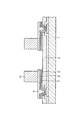
図1はこの発明の一実施形態としての半導体装置の断面図を示す。この半導体装置は、一般的にはCSP(chip size package)と呼ばれるものであり、シリコン基板(半導体基板)1を備えている。シリコン基板1の上面には所定の機能の集積回路(図示せず)が設けられ、上面周辺部にはアルミニウムやアルミニウム合金などのアルミニウム系金属からなる複数の接続パッド2が集積回路に接続されて設けられている。
FIG. 1 is a sectional view of a semiconductor device as an embodiment of the present invention. This semiconductor device is generally called a CSP (chip size package) and includes a silicon substrate (semiconductor substrate) 1. An integrated circuit (not shown) having a predetermined function is provided on the upper surface of the
接続パッド2の中央部を除くシリコン基板1の上面には酸化シリコン、窒化シリコン、テオスなどからなる絶縁膜3が設けられ、接続パッド2の中央部は絶縁膜3に設けられた開口部4を介して露出されている。絶縁膜3の上面にはポリイミドやポリベンゾオキサイド(PBO)などからなる保護膜5が設けられている。この場合、保護膜5の上面側において後述する第1の下地金属層7下には、後で説明するように、変質層(以下、この変質層を変質層Cという)がパターン形成されている。また、絶縁膜3の開口部4に対応する部分における変質層Cを含む保護膜5には、絶縁膜3の開口部4よりもやや大きめの開口部6が設けられている。
An
絶縁膜3および変質層Cを含む保護膜5の開口部4、6内および変質層Cの上面全体にはチタンやクロムなどからなる第1の下地金属層7が設けられている。第1の下地金属層7の上面全体には銅からなる第2の下地金属層8が設けられている。第2の下地金属層8の上面全体には銅からなる配線9が設けられている。第1、第2の下地金属層7、8を含む配線9の一端部は、絶縁膜3および変質層Cを含む保護膜5の開口部4、6を介して接続パッド2に接続されている。
A first
配線9の接続パッド部上面には銅からなる柱状電極10が設けられている。配線9を含む保護膜5の上面にはエポキシ系樹脂やフェノール系樹脂などからなる封止膜11がその上面が柱状電極10の上面と面一となるように設けられている。柱状電極10の上面には半田ボール12が設けられている。
A
次に、この半導体装置の製造方法の一例について説明する。まず、図2に示すように、ウエハ状態のシリコン1(半導体基板)上にアルミニウム系金属からなる複数の接続パッド2および酸化シリコンなどからなる絶縁膜3が設けられ、接続パッド2の中央部が絶縁膜3に形成された開口部4を介して露出されたものを用意する。この場合、ウエハ状態のシリコン基板1には、各半導体装置が形成される領域に所定の機能の集積回路(図示せず)が形成され、接続パッド2は、それぞれ、対応する領域に形成された集積回路に電気的に接続されている。
Next, an example of a method for manufacturing this semiconductor device will be described. First, as shown in FIG. 2, a plurality of
次に、図3に示すように、絶縁膜3の開口部4を介して露出された接続パッド2の上面を含む絶縁膜3の上面全体に、スクリーン印刷法やスピンコート法などにより、ポリイミドやPBOなどからなる保護膜5を形成する。次に、フォトリソグラフィ法により、絶縁膜3の開口部3に対応する部分における保護膜5に、絶縁膜3の開口部4よりもやや大きめの開口部6を形成する。
Next, as shown in FIG. 3, the entire upper surface of the
ここで、ポリイミドやPBOなどの樹脂からなる保護膜5に開口部6を形成したとき、保護膜5の開口部6を介して露出された接続パッド2の上面にスカムと呼ばれるポリイミドやPBOなどの樹脂からなる残渣(図示せず)が残存する場合がある。そこで、次に、この残渣を酸素プラズマアッシングにより除去する。この場合、図4に示すように、保護膜5の上面層が酸素プラズマの影響を受けて変質し、変質層Aが形成される。
Here, when the
次に、絶縁膜3および変質層Aを含む保護膜5の開口部4、6を介して露出されたアルミニウム系金属からなる接続パッド2の上面に形成された自然酸化膜(図示せず)をアルゴンガスなどの不活性ガスを用いたプラズマエッチングにより除去する。このようなプラズマエッチングにより、変質層Aがさらに変質して変質層Cが形成される。不活性ガスを用いたプラズマエッチングの方式としては、1周波励起または2周波励起の反応性イオンエッチング(RIE)、ヘリコン波励起型反応性高密度プラズマ、2周波励起の誘導結合型プラズマ(ICP、inductively coupled plasma)、ISM(inductively super magneron)などがあり、特に、2周波励起のICP、ISMを用いたプラズマエッチングが好ましい。
Next, a natural oxide film (not shown) formed on the upper surface of the
ここで、図3に示す保護膜5の上面のSEM(走査型電子顕微鏡)写真である図12(A)を見ると、上面がほぼ平坦であり、変質層は形成されていない。次に、変質層Aの上面のSEM写真である図12(B)を見ると、上面が10〜100nmの凸凹構造となっており、変質層Aが形成されている。次に、変質層Cの上面のSEM写真である図12(C)を見ると、変質層Aよりも表面粗さが粗い網目構造となっており、変質層Cが形成されている。
Here, referring to FIG. 12A, which is an SEM (scanning electron microscope) photograph of the upper surface of the
この場合、変質層Cの網目の直径は10〜500nm、網の太さは10〜200nm、層厚は10〜1000nmである。また、保護膜5の材料であるポリイミドあるいはPBOの構成元素が炭素、酸素、窒素、水素であるので、変質層Cの構成元素は炭素、酸素、窒素、水素、不活性ガスとなる。この場合、変質層Cに含まれる不活性ガスは、不活性ガスとしてアルゴンガスを用いたプラズマエッチング処理ではアルゴンガスである。なお、変質層Aの構成元素は、保護膜5と同じで、炭素、酸素、窒素、水素である。
In this case, the modified layer C has a mesh diameter of 10 to 500 nm, a mesh thickness of 10 to 200 nm, and a layer thickness of 10 to 1000 nm. Further, since the constituent elements of polyimide or PBO, which is the material of the
ところで、接続パッド2の上面の自然酸化膜を除去するために、アルゴンガスを用いたプラズマエッチングの代わりに、イオンガン方式によるアルゴンイオンエッチングを行なった場合には、保護膜5の上面側に、変質層Cではなく、変質層Bが形成される。そして、変質層Bの上面のSEM写真である図12(D)を見ると、図12(B)に示す変質層Aで見られた凸凹が減少して、図12(A)に示す保護膜5の上面に近い状態となっている。
By the way, in order to remove the natural oxide film on the upper surface of the
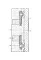
次に、図5に示すように、絶縁膜3および変質層Cを含む保護膜5の開口部4、6を介して露出された接続パッド2の上面を含む変質層Cの上面全体に、スパッタ法などにより、チタンやクロムなどからなる第1の下地金属層7および銅からなる第2の下地金属層8を連続して成膜する。この場合、第1の下地金属層7は変質層Cの上面に成膜されるため、後で説明するように、その界面の密着力は高い。なお、下地金属層は、接着機能とバリア機能を有するものであれば1層とすることもできる。
Next, as shown in FIG. 5, the entire upper surface of the altered layer C including the upper surface of the
次に、第2の下地金属層8の上面にメッキレジスト膜21をパターン形成する。この場合、配線9形成領域に対応する部分におけるメッキレジスト膜21には開口部22が形成されている。次に、第1、第2の下地金属層7、8をメッキ電流路として銅の電解メッキを行なうことにより、メッキレジスト膜21の開口部22内の第2の下地金属層8の上面に配線9を形成する。次に、メッキレジスト膜21を剥離する。なお、下地金属層を厚く形成することにより下地金属層のみからなる配線とすることも可能である。
Next, a plating resist
次に、図6に示すように、配線9を含む第2の下地金属層8の上面にメッキレジスト膜23をパターン形成する。この場合、柱状電極10形成領域に対応する部分におけるメッキレジスト膜23には開口部24が形成されている。次に、第1、第2の下地金属層7、8をメッキ電流路として銅の電解メッキを行なうことにより、メッキレジスト膜23の開口部24内の配線9の接続パッド部上面に柱状電極10を形成する。
Next, as shown in FIG. 6, a plating resist film 23 is patterned on the upper surface of the second
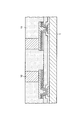
次に、メッキレジスト膜23を剥離し、次いで、配線9をマスクとして第1、第2の下地金属層7、8の不要な部分をエッチングして除去すると、図7に示すように、配線9下にのみ第1、第2の下地金属層7、8が残存される。
Next, the plating resist film 23 is peeled off, and then unnecessary portions of the first and second
この状態では、第1の下地金属層7下以外の領域における保護膜5の上面にも変質層Cが形成されている。変質層Cは導電性を有するため、このままでは、配線9間でショートが生じてしまう。そこで、次に、第1の下地金属層7下以外の領域における変質層Cを酸素プラズマアッシングにより除去すると、図8に示すように、第1の下地金属層7下にのみ変質層Cが残存される。
In this state, the altered layer C is also formed on the upper surface of the
この場合の酸素プラズマアッシングとしては、ICP(Inductively Coupled Plasma)タイプのプラズマアッシング装置を用い、ウエハ1枚に対して、酸素量200〜500sccm、プラズマパワー500〜1000W、圧力20〜133Pa、ステージ温度40〜80℃、処理時間10〜60secの条件で行なった。 As oxygen plasma ashing in this case, an ICP (Inductively Coupled Plasma) type plasma ashing apparatus is used. The oxygen amount is 200 to 500 sccm, the plasma power is 500 to 1000 W, the pressure is 20 to 133 Pa, and the stage temperature is 40 for one wafer. It was carried out under conditions of ˜80 ° C. and treatment time of 10 to 60 seconds.
すると、オーバーアッシングとなり、第1の下地金属層7下以外の領域における保護膜の上面側の一部も除去され、第1の下地金属層7下以外の領域における変質層Cが完全に除去された。この場合、第1の下地金属層7下以外の領域における保護膜5の上面層が酸素プラズマの影響を受けて変質し、変質層Aが形成されるが、別に支障はない。
Then, overashing occurs, and a part of the upper surface side of the protective film in a region other than the region under the first
次に、図9に示すように、柱状電極10および配線9を含む保護膜5の上面全体に、スクリーン印刷法やスピンコート法などにより、エポキシ系樹脂などからなる封止膜11をその厚さが柱状電極10の高さよりも厚くなるように形成する。したがって、この状態では、柱状電極10の上面は封止膜11によって覆われている。
Next, as shown in FIG. 9, the sealing
次に、封止膜11および柱状電極10の上面側を適宜に研磨し、図10に示すように、柱状電極10の上面を露出させ、且つ、この露出された柱状電極10の上面を含む封止膜11の上面を平坦化する。次に、図11に示すように、柱状電極10の上面に半田ボール11を形成する。次に、ダイシング工程を経ると、図1に示す半導体装置が複数個得られる。
Next, the upper surface side of the sealing
このようにして得られた半導体装置では、ポリイミドやPBOなどからなる保護膜5の上面側に、変質層Bではなく、網目構造の変質層Cを形成しているので、この網目構造の変質層Cのチタンやクロムなどからなる第1の下地金属層7に対する密着力を、次に説明するように、向上させることができる。
In the semiconductor device thus obtained, the modified layer C having a network structure is formed instead of the modified layer B on the upper surface side of the
次に、上記製造方法により製造された半導体装置のプレッシャークッカーテスト(PCT)によるシェア強度試験について説明する。この場合、図13に示す本発明品を用意した。この本発明品は、シリコン基板1の上面にポリイミドからなる保護膜5が形成され、保護膜5の上面に変質層Cが形成され、変質層Cの上面に平面円形状のチタンからなる第1の下地金属層7、銅からなる第2の下地金属層8および銅からなる柱状電極10が形成された構造となっている。また、比較のために、図13に示す本発明品と同じ構造であるが、保護膜5の上面に変質層Bが形成された比較品を用意した。
Next, the shear strength test by the pressure cooker test (PCT) of the semiconductor device manufactured by the above manufacturing method will be described. In this case, the product of the present invention shown in FIG. 13 was prepared. In the product of the present invention, a
そして、本発明品および比較品について、シリコン基板1を固定した状態で、柱状電極10の側面にシェア測定治具(図示せず)を押し付けて、第1の下地金属層7が変質層C(B)から剥離したときの強度(g)を求めた。この場合、本発明品および比較品共に、環境試験投入前のシェア強度を1とし、PCTの飽和(温度121℃、湿度100%Rh、2気圧)に500時間放置した後でのシェア強度を求めた。
Then, for the product of the present invention and the comparative product, with the
すると、比較品の場合には、環境試験投入前のシェア強度を1としたとき、PCTの飽和に500時間放置した後でのシェア強度は0.1まで低下した。これに対し、本発明品の場合には、環境試験投入前のシェア強度を1としたとき、PCTの飽和に500時間放置した後でのシェア強度は0.68まで低下したが、比較品の6.8倍であり、界面密着力が向上したと言える。 Then, in the case of the comparative product, when the shear strength before the environmental test was set to 1, the shear strength after leaving for 500 hours in the saturation of the PCT decreased to 0.1. On the other hand, in the case of the product of the present invention, when the shear strength before the environmental test was set to 1, the shear strength after leaving for 500 hours at the saturation of PCT decreased to 0.68. It was 6.8 times, and it can be said that the interfacial adhesion was improved.
なお、この発明は、CSPと呼ばれる半導体装置に限らず、例えば、上記従来例の如く、半導体基板上に複数の接続パッド、絶縁膜、保護膜が設けられ、接続パッドが絶縁膜および保護膜に設けられた開口部を介して露出され、この露出された接続パッドの上面およびその近傍の保護膜の上面に第1、第2の下地金属層およびバンプ電極が設けられたものにも適用することができる。 The present invention is not limited to a semiconductor device called a CSP. For example, as in the above-described conventional example, a plurality of connection pads, insulating films, and protective films are provided on a semiconductor substrate, and the connection pads are formed as insulating films and protective films. The present invention is also applicable to the case where the first and second base metal layers and the bump electrode are provided on the upper surface of the exposed connection pad and the protective film in the vicinity thereof exposed through the provided opening. Can do.
1 シリコン基板
2 接続パッド
3 絶縁膜
4 開口部
5 保護膜
6 開口部
7 第1の下地金属層
8 第2の下地金属層
9 配線
10 柱状電極
11 封止膜
12 半田ボール
A 変質層A
B 変質層B
C 変質層C
DESCRIPTION OF
B Altered layer B
C Altered layer C
Claims (13)
前記保護膜の開口部を介して露出された前記接続パッドの上面に残存された前記保護膜の残渣を酸素プラズマアッシングにより除去し、当該酸素プラズマアッシングにより前記保護膜の上面層が変質された変質層Aが形成される工程と、
前記保護膜の開口部を介して露出された前記接続パッドの上面に形成された酸化膜を、不活性ガスを用いたプラズマエッチングにより除去し、当該プラズマエッチングにより前記変質層Aが変質され、当該変質層よりも表面粗さが粗い変質層Cが形成される工程と、
前記保護膜の開口部を介して露出された前記接続パッドの上面および前記変質層Cの上面に金属層をパターン形成する工程と、
前記金属層下以外の領域における前記変質層Cを酸素プラズマアッシングにより除去する工程と、
を有することを特徴とする半導体装置の製造方法。 Forming a protective film made of a resin having an opening in a portion corresponding to the connection pad on a semiconductor substrate having a plurality of connection pads on the upper surface;
Deterioration in which the residue of the protective film remaining on the upper surface of the connection pad exposed through the opening of the protective film is removed by oxygen plasma ashing, and the upper surface layer of the protective film is altered by the oxygen plasma ashing The step of forming layer A;
The oxide film formed on the upper surface of the connection pad exposed through the opening of the protective film is removed by plasma etching using an inert gas, and the altered layer A is altered by the plasma etching. A step of forming a modified layer C having a rougher surface roughness than the modified layer;
Patterning a metal layer on the upper surface of the connection pad and the upper surface of the altered layer C exposed through the opening of the protective film;
Removing the altered layer C in a region other than under the metal layer by oxygen plasma ashing;
A method for manufacturing a semiconductor device, comprising:
Priority Applications (2)
| Application Number | Priority Date | Filing Date | Title |
|---|---|---|---|
| JP2005275631A JP2006270031A (en) | 2005-02-25 | 2005-09-22 | Semiconductor device and its manufacturing method |
| US11/524,455 US20070085224A1 (en) | 2005-09-22 | 2006-09-20 | Semiconductor device having strong adhesion between wiring and protective film, and manufacturing method therefor |
Applications Claiming Priority (2)
| Application Number | Priority Date | Filing Date | Title |
|---|---|---|---|
| JP2005050342 | 2005-02-25 | ||
| JP2005275631A JP2006270031A (en) | 2005-02-25 | 2005-09-22 | Semiconductor device and its manufacturing method |
Related Child Applications (1)
| Application Number | Title | Priority Date | Filing Date |
|---|---|---|---|
| JP2011092610A Division JP5170915B2 (en) | 2005-02-25 | 2011-04-19 | Manufacturing method of semiconductor device |
Publications (1)
| Publication Number | Publication Date |
|---|---|
| JP2006270031A true JP2006270031A (en) | 2006-10-05 |
Family
ID=37205609
Family Applications (1)
| Application Number | Title | Priority Date | Filing Date |
|---|---|---|---|
| JP2005275631A Pending JP2006270031A (en) | 2005-02-25 | 2005-09-22 | Semiconductor device and its manufacturing method |
Country Status (1)
| Country | Link |
|---|---|
| JP (1) | JP2006270031A (en) |
Cited By (4)
| Publication number | Priority date | Publication date | Assignee | Title |
|---|---|---|---|---|
| JP2010062175A (en) * | 2008-09-01 | 2010-03-18 | Casio Comput Co Ltd | Method for manufacturing semiconductor device |
| JP2011014749A (en) * | 2009-07-02 | 2011-01-20 | Fuji Electric Systems Co Ltd | Method for manufacturing semiconductor device |
| JP2012114148A (en) * | 2010-11-22 | 2012-06-14 | Fujitsu Semiconductor Ltd | Method of manufacturing semiconductor device |
| KR20180021034A (en) * | 2015-12-16 | 2018-02-28 | 타이완 세미콘덕터 매뉴팩쳐링 컴퍼니 리미티드 | Semiconductor device structure and method for forming the same |
Citations (4)
| Publication number | Priority date | Publication date | Assignee | Title |
|---|---|---|---|---|
| JPH07130750A (en) * | 1993-11-05 | 1995-05-19 | Casio Comput Co Ltd | Manufacture of semiconductor device having bump electrode |
| JPH11238750A (en) * | 1998-02-23 | 1999-08-31 | Sony Corp | Manufacture of bump and manufacture of semiconductor device |
| JP2002093948A (en) * | 2000-07-13 | 2002-03-29 | Oki Electric Ind Co Ltd | Wafer and its manufacturing method |
| JP2004349461A (en) * | 2003-05-22 | 2004-12-09 | Casio Comput Co Ltd | Method of manufacturing semiconductor device |
-
2005
- 2005-09-22 JP JP2005275631A patent/JP2006270031A/en active Pending
Patent Citations (4)
| Publication number | Priority date | Publication date | Assignee | Title |
|---|---|---|---|---|
| JPH07130750A (en) * | 1993-11-05 | 1995-05-19 | Casio Comput Co Ltd | Manufacture of semiconductor device having bump electrode |
| JPH11238750A (en) * | 1998-02-23 | 1999-08-31 | Sony Corp | Manufacture of bump and manufacture of semiconductor device |
| JP2002093948A (en) * | 2000-07-13 | 2002-03-29 | Oki Electric Ind Co Ltd | Wafer and its manufacturing method |
| JP2004349461A (en) * | 2003-05-22 | 2004-12-09 | Casio Comput Co Ltd | Method of manufacturing semiconductor device |
Cited By (9)
| Publication number | Priority date | Publication date | Assignee | Title |
|---|---|---|---|---|
| JP2010062175A (en) * | 2008-09-01 | 2010-03-18 | Casio Comput Co Ltd | Method for manufacturing semiconductor device |
| JP2011014749A (en) * | 2009-07-02 | 2011-01-20 | Fuji Electric Systems Co Ltd | Method for manufacturing semiconductor device |
| JP2012114148A (en) * | 2010-11-22 | 2012-06-14 | Fujitsu Semiconductor Ltd | Method of manufacturing semiconductor device |
| KR20180021034A (en) * | 2015-12-16 | 2018-02-28 | 타이완 세미콘덕터 매뉴팩쳐링 컴퍼니 리미티드 | Semiconductor device structure and method for forming the same |
| US10163817B2 (en) | 2015-12-16 | 2018-12-25 | Taiwan Semiconductor Manufacturing Co., Ltd. | Semiconductor device structure comprising a plurality of metal oxide fibers and method for forming the same |
| KR101939531B1 (en) | 2015-12-16 | 2019-01-16 | 타이완 세미콘덕터 매뉴팩쳐링 컴퍼니 리미티드 | Semiconductor device structure and method for forming the same |
| US10224293B2 (en) | 2015-12-16 | 2019-03-05 | Taiwan Semiconductor Manufacturing Company, Ltd. | Package structure and method for forming the same |
| US10636748B2 (en) | 2015-12-16 | 2020-04-28 | Taiwan Semiconductor Manufacturing Co., Ltd. | Package structure |
| US10943873B2 (en) | 2015-12-16 | 2021-03-09 | Taiwan Semiconductor Manufacturing Co., Ltd. | Semiconductor device structure comprising a plurality of metal oxide fibers and method for forming the same |
Similar Documents
| Publication | Publication Date | Title |
|---|---|---|
| US8723322B2 (en) | Method of metal sputtering for integrated circuit metal routing | |
| US6936923B2 (en) | Method to form very a fine pitch solder bump using methods of electroplating | |
| CN1988143B (en) | Semiconductor device and manufacturing method of the same | |
| US6605524B1 (en) | Bumping process to increase bump height and to create a more robust bump structure | |
| US20060175686A1 (en) | Semiconductor device and fabrication method thereof | |
| JP2011166072A (en) | Semiconductor device and method of manufacturing the same | |
| TW200832641A (en) | Semiconductor device having projecting electrode formed by electrolytic plating, and manufacturing method thereof | |
| WO2008091023A1 (en) | Semiconductor device comprising electromigration prevention film and manufacturing method thereof | |
| JP4765947B2 (en) | Semiconductor device and manufacturing method thereof | |
| JP2009177072A (en) | Semiconductor device, and manufacturing method thereof | |
| US8309373B2 (en) | Method of manufacturing semiconductor device | |
| JP2006270031A (en) | Semiconductor device and its manufacturing method | |
| JP5170915B2 (en) | Manufacturing method of semiconductor device | |
| JP4506767B2 (en) | Manufacturing method of semiconductor device | |
| US20070085224A1 (en) | Semiconductor device having strong adhesion between wiring and protective film, and manufacturing method therefor | |
| JP2006049427A (en) | Method for manufacturing semiconductor device | |
| US7772699B2 (en) | Semiconductor device and method of manufacturing the same | |
| JP2011071175A (en) | Semiconductor device and method of manufacturing the same | |
| JP4686962B2 (en) | Manufacturing method of semiconductor device | |
| JP2013207067A (en) | Semiconductor device and manufacturing method of the same | |
| JP2007258354A (en) | Process for manufacturing semiconductor device | |
| JP2005129665A (en) | Semiconductor device and manufacturing method thereof | |
| JPH09306918A (en) | Barrier metal forming method in forming process of solder ball bump | |
| JPH10224029A (en) | Production of bump | |
| JP2007035875A (en) | Semiconductor device and its manufacturing method |
Legal Events
| Date | Code | Title | Description |
|---|---|---|---|
| A621 | Written request for application examination |
Free format text: JAPANESE INTERMEDIATE CODE: A621 Effective date: 20061129 |
|
| RD04 | Notification of resignation of power of attorney |
Free format text: JAPANESE INTERMEDIATE CODE: A7424 Effective date: 20080515 |
|
| A977 | Report on retrieval |
Free format text: JAPANESE INTERMEDIATE CODE: A971007 Effective date: 20090123 |
|
| A131 | Notification of reasons for refusal |
Free format text: JAPANESE INTERMEDIATE CODE: A131 Effective date: 20101102 |
|
| A521 | Written amendment |
Free format text: JAPANESE INTERMEDIATE CODE: A523 Effective date: 20101228 |
|
| A131 | Notification of reasons for refusal |
Free format text: JAPANESE INTERMEDIATE CODE: A131 Effective date: 20110301 |
|
| A521 | Written amendment |
Free format text: JAPANESE INTERMEDIATE CODE: A523 Effective date: 20110419 |
|
| A711 | Notification of change in applicant |
Free format text: JAPANESE INTERMEDIATE CODE: A712 Effective date: 20111108 |
|
| A521 | Written amendment |
Free format text: JAPANESE INTERMEDIATE CODE: A821 Effective date: 20111108 |
|
| A521 | Written amendment |
Free format text: JAPANESE INTERMEDIATE CODE: A523 Effective date: 20111216 |
|
| A521 | Written amendment |
Free format text: JAPANESE INTERMEDIATE CODE: A821 Effective date: 20111216 |
|
| A02 | Decision of refusal |
Free format text: JAPANESE INTERMEDIATE CODE: A02 Effective date: 20120131 |