JP2006268656A - Internal power supply control method, internal power supply circuit and semiconductor device - Google Patents
Internal power supply control method, internal power supply circuit and semiconductor device Download PDFInfo
- Publication number
- JP2006268656A JP2006268656A JP2005088465A JP2005088465A JP2006268656A JP 2006268656 A JP2006268656 A JP 2006268656A JP 2005088465 A JP2005088465 A JP 2005088465A JP 2005088465 A JP2005088465 A JP 2005088465A JP 2006268656 A JP2006268656 A JP 2006268656A
- Authority
- JP
- Japan
- Prior art keywords
- power supply
- circuit
- frequency
- internal power
- supply circuit
- Prior art date
- Legal status (The legal status is an assumption and is not a legal conclusion. Google has not performed a legal analysis and makes no representation as to the accuracy of the status listed.)
- Pending
Links
Images


Classifications
-
- G—PHYSICS
- G06—COMPUTING; CALCULATING OR COUNTING
- G06F—ELECTRIC DIGITAL DATA PROCESSING
- G06F1/00—Details not covered by groups G06F3/00 - G06F13/00 and G06F21/00
- G06F1/26—Power supply means, e.g. regulation thereof
- G06F1/263—Arrangements for using multiple switchable power supplies, e.g. battery and AC
Abstract
Description
本発明は、内部電源の制御方法、この制御方法を用いた内部電源回路、およびこの内部電源回路を含む半導体装置に関する。 The present invention relates to an internal power supply control method, an internal power supply circuit using the control method, and a semiconductor device including the internal power supply circuit.
近年、マイクロプロセッサの高速化及び低消費電力化に伴い、データ転送速度の速いチップかつ低消費電力化が可能なチップの要求が高まっている。顧客のこのような要求を満足させるため、高速動作が可能でかつ消費電力を抑えることができるチップの開発が行われている。特に、高速動作するDLL(Delay Locked Loop)回路の消費電流削減は必要不可欠である。周知のように、クロック周波数が高いほど、その消費電力は増大する。一方、量産による原価低減を図り、DLL回路は多種類の装置に適用できるように、想定される最高周波数に合わせて設計されている。しかしながら、DLL回路は、備えられる半導体装置によっては設計された周波数より大幅に低い周波数で使用される場合がある。 In recent years, with the increase in speed and power consumption of microprocessors, there has been an increasing demand for chips with a high data transfer speed and capable of reducing power consumption. In order to satisfy such requirements of customers, a chip capable of high-speed operation and suppressing power consumption has been developed. In particular, it is indispensable to reduce current consumption of a DLL (Delay Locked Loop) circuit that operates at high speed. As is well known, the higher the clock frequency, the greater the power consumption. On the other hand, in order to reduce the cost by mass production, the DLL circuit is designed in accordance with the assumed maximum frequency so that it can be applied to various kinds of devices. However, the DLL circuit may be used at a frequency significantly lower than the designed frequency depending on the semiconductor device provided.
このようなクロックの高速化に伴う状態を配慮し、現状のDLL回路では、量1産化に適した内部電源として、小容量の小型化された複数の電源回路が設置される場合がある。すなわち、DLL回路に一定の電流供給能力を持つ電源回路が複数台設置されることがある。この場合、低速クロックで動作するDLL回路では消費電流が少ないので、複数台の電源回路は不要である。 In consideration of the state accompanying the increase in the clock speed, there are cases where a plurality of small-sized power supply circuits having a small capacity are installed as an internal power supply suitable for mass production in the current DLL circuit. That is, a plurality of power supply circuits having a constant current supply capability may be installed in the DLL circuit. In this case, since the current consumption is small in the DLL circuit operating with the low-speed clock, a plurality of power supply circuits are unnecessary.
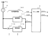
図1から図4までを参照してこの種のDLL回路2を含む半導体装置に実際に使用されている内部電源回路100とその周辺回路の一例を説明する。
An example of the internal
図示される内部電源回路100は、二つの電源回路111,112を有し、外部電源電圧VDDを電流電源3から配線を介して受け、DLL回路2に供給するように降圧した内部電源電圧VPERIを出力する。図1では、低速クロックのDLL回路に使用される場合の構成を示し、このため、電源回路112に対する配線110が切断されている。この結果、外部電源電圧VDDは一方の電源回路111のみに供給され、他方の内部電源回路112には供給されない。
The illustrated internal
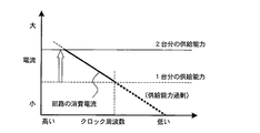
図2に示されるように、図1の構成では、低いクロック周波数に対してのみ対応できる構成であり、高いクロック周波数には対応できない。しかし、電源回路112に電流供給されないので、図1の回路構成は低消費電流である。
As shown in FIG. 2, the configuration of FIG. 1 is a configuration that can cope only with a low clock frequency and cannot cope with a high clock frequency. However, since no current is supplied to the
他方、図3で示されるように、高速クロックのDLL回路に使用される場合、配線、例えば、アルミニウム配線110によって、二つの電源回路111,112はDLL回路2に接続され、この結果、DLL回路2には両電源回路111、112から電流が供給される。従って、図4に示されるように、高速クロック対応で使用できる。しかしながら、この回路構成を低速クロック動作で使用する場合には、供給能力の過剰となり、不必要な消費電流が発生する。
On the other hand, as shown in FIG. 3, when used in a high-speed clock DLL circuit, the two
上述したように、高速クロックまたは低速クロックに対応するためには、内部電源回路100の電源回路111,112に対する配線110を接続または切断することが必要である。しかし、この回路構成では、チップ化された内部電源を高速/低速クロックに対して顧客側で任意に切り替えることは不可能である。
As described above, in order to cope with the high-speed clock or the low-speed clock, it is necessary to connect or disconnect the
すなわち、図1および図3に示されるように、供給電力の適正化を図るためにDLL回路に対する内部電源回路を複数回路に分割した場合、その消費電流の調整をアルミニウム配線の接続または切断という処理により実行するため、顧客自身で採用すべき内部電源の適正化が困難または不可能なことである。 That is, as shown in FIGS. 1 and 3, when the internal power supply circuit for the DLL circuit is divided into a plurality of circuits in order to optimize the supply power, the adjustment of the current consumption is a process of connecting or disconnecting the aluminum wiring. Therefore, it is difficult or impossible to optimize the internal power supply that should be adopted by the customer.
本発明の目的は、レイアウトの修正を必要としない内部電源制御方法を提供することである。 An object of the present invention is to provide an internal power supply control method that does not require layout modification.
本発明は、外部入力するクロックの周波数により消費電流が大きく変わる特性を有している電子回路に供給される外部入力クロック周波数を検知して供給電流を制御し、無駄な消費電流を削減する内部電源制御方法、この制御方法を用いた内部電源回路、およびこの内部電源回路を備えた半導体装置、特に、DRAM(ダイナミック・ランダム・アクセス・メモリ)に代表される高速メモリ等に入力されるデータの位相を内部クロックの位相に同期させる半導体記憶装置に関するものである。 The present invention detects an external input clock frequency supplied to an electronic circuit having a characteristic that the consumption current greatly varies depending on the frequency of an externally input clock, and controls the supply current to reduce useless consumption current. Power supply control method, internal power supply circuit using this control method, and semiconductor device equipped with this internal power supply circuit, in particular, high-speed memory represented by DRAM (dynamic random access memory) The present invention relates to a semiconductor memory device whose phase is synchronized with the phase of an internal clock.
すなわち、本発明は、顧客がチップ化された内部電源回路を使用する際に適用すべき高速/低速クロックを意識することなく使用可能とするため、内部電源回路を分割し、この分割された複数の電源回路を外部電源とDLL回路のようなクロックで動作する電子回路との間に並列配備し、周波数判定回路により上記クロックを取り込んでその周波数を検出し、この検出した周波数に基づいて上記複数の電源回路それぞれの電子回路との接続を制御することを主要な特徴とする。 That is, the present invention divides the internal power supply circuit so that the customer can use it without being aware of the high-speed / low-speed clock to be applied when using the chip-formed internal power supply circuit. Are arranged in parallel between an external power supply and an electronic circuit that operates with a clock such as a DLL circuit, the clock is taken in by a frequency determination circuit, and the frequency is detected. The main feature is to control the connection of each power circuit to the electronic circuit.
すなわち、検出した周波数が所定の周波数を越えた場合には全ての電源回路を動作させ、その周波数より低い場合には一部の電源回路を、全く電流消費させないよう完全に動作停止させておくというように、本発明はこの周波数判定により分割された電源回路の稼動台数制御を行うことを特徴としている。 That is, when the detected frequency exceeds a predetermined frequency, all the power supply circuits are operated. When the detected frequency is lower than the predetermined frequency, some power supply circuits are completely stopped so as not to consume any current. Thus, the present invention is characterized in that the number of operating power supply circuits divided by this frequency determination is controlled.
上記分割された電源回路は、外部電源と電子回路とを常時接続する一つの基本電源回路と、周波数に基づく条件付で接続または切断する少なくとも一つの付加電源回路とを備えることが制御の簡潔化のため望ましい。更に、上記複数の電源回路のうち少なくとも付加電源回路は、それぞれが電流の同一供給能力を有していることがその制御の簡素化上、好ましい。 The divided power supply circuit includes one basic power supply circuit that always connects an external power supply and an electronic circuit, and at least one additional power supply circuit that is connected or disconnected conditionally based on frequency. Desirable for. Furthermore, it is preferable for simplification of control that at least the additional power supply circuit among the plurality of power supply circuits has the same current supply capability.
本発明による電源制御は、外部入力するクロック周波数により消費電流が大きく変わる特性を有している電子回路に供給する内部電源を制御する際、その内部電源のための回路を複数の電源回路に分割し、動作対象となるクロック周波数を検出し、かつこのクロック周波数に適するように上記複数の電源回路の接続を制御している。すなわち、本発明による内部電源回路を配備することにより、必要に応じて自動的に適正化された数の電源回路を電子回路に接続できる。従って、消費電流適正化のための高速/低速クロックに対する顧客による配線処理を不要にできるという利点がある。 The power control according to the present invention divides a circuit for the internal power supply into a plurality of power supply circuits when controlling the internal power supply supplied to the electronic circuit having the characteristic that the consumption current greatly varies depending on the clock frequency inputted externally. Then, the clock frequency to be operated is detected, and the connection of the plurality of power supply circuits is controlled so as to be suitable for this clock frequency. In other words, by arranging the internal power supply circuit according to the present invention, the number of power supply circuits automatically optimized as necessary can be connected to the electronic circuit. Therefore, there is an advantage that the wiring processing by the customer for the high speed / low speed clock for optimizing the current consumption can be eliminated.
本発明では、クロックを用いる電子回路を使用する際、外部電源と上記電子回路との間を接続し、外部電源を受け電子回路に供給する内部電源回路の配備に際して高速/低速のクロックに対応する顧客による配線処理を不要にすることである。このため、本発明では、内部電源回路を複数の電源回路に分割しておき、上記クロックを取り込んでその周波数を検出し、検出した周波数に基づいて複数の上記電源回路それぞれの電子回路との接続/非接続を制御する構成により実現された。 In the present invention, when an electronic circuit using a clock is used, an external power supply is connected to the electronic circuit, and an internal power supply circuit that receives the external power supply and supplies the electronic circuit corresponds to a high-speed / low-speed clock. It is to eliminate the wiring process by the customer. For this reason, in the present invention, the internal power supply circuit is divided into a plurality of power supply circuits, the clock is taken in, the frequency is detected, and the connection to the electronic circuits of each of the plurality of power supply circuits is performed based on the detected frequency. / Realized by a configuration that controls disconnection.
複数の電源回路の少なくとも一つは常時接続する基本電源回路であり、他の少なくとも一つは処理する周波数に基づく条件付で接続する付加電源回路である構成を有し、特に、基本電源回路は一つであることが、接続制御上、望ましい。また、周波数判定回路が上記クロックを取り込んでその周波数を検出し、検出した周波数に基づいて上記付加電源回路の接続を制御することになる。この結果、電子回路で使用するクロック周波数に適正化された数の電源回路が、外部電源と電子回路との間に並列接続される。 At least one of the plurality of power supply circuits is a basic power supply circuit that is always connected, and at least one of the other power supply circuits is an additional power supply circuit that is connected conditionally based on the frequency to be processed. One is desirable in connection control. Further, the frequency determination circuit captures the clock and detects the frequency, and controls the connection of the additional power supply circuit based on the detected frequency. As a result, a number of power supply circuits optimized for the clock frequency used in the electronic circuit are connected in parallel between the external power supply and the electronic circuit.
本発明の実施例1について図5および図6を併せ参照して説明する。
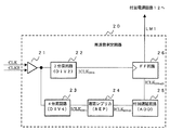
図5は、本発明による実施例1として、内部電源回路1とその周辺回路との機能ブロックの一構成を示す説明図である。図5では、内部電源回路1、DLL(Delay Locked Loop)回路2、および外部電流源A3とが示されている。外部電流源A3は外部電源電圧VDDを受けて内部電源回路1に電流を供給する回路である。
FIG. 5 is an explanatory diagram showing one configuration of functional blocks of the internal
内部電源回路1は、DLL回路2と外部電源電圧VDDを有する外部電流源A3との間に配備され、外部電源電圧VDDを受けて内部電源電圧VPERIに降圧しDLL回路2に供給する動作を行い、基本電源回路11、付加電源回路12、および周波数判定回路20によって構成されている。
Internal
DLL回路2は、外部入力するクロック周波数により消費電流が大きく変わる特性を有している代表的な回路であり、内部電源電圧VPERIおよびクロックCLK,CLKBを入力して動作する。
The
内部電源回路1の基本電源回路11は、高周波数状態で動作するDLL回路2の最大消費電流に対してほぼ半分の電流をまかなう、または、例えば半導体記憶装置がスタンバイ/アクティブ状態のような低周波数状態の場合に適切な小電流を供給する。
The basic
付加電源回路12は、基本電源回路11と並列に協動して、高周波数状態で動作するDLL回路2の最大消費電流に対して十分な電流を供給する。
The additional
周波数判定回路20は、DLL回路2に入力されるクロックと同一のクロックCLK,CLKBを入力してこのクロック周波数を検出判定し、付加電源回路12へ通知する。
The
図6は、図5における基本電源回路11および付加電源回路12の作動状態を説明するための特性を示し、ここでは、クロック周波数とDLL回路2へ供給する電流との関係を示している。
FIG. 6 shows characteristics for explaining the operating states of the basic
すなわち、付加電源回路12はクロックの高速化に伴いDLL回路2への供給能力を上げるために追加されるが、低速クロックの際には無駄な消費が発生することになる。従って、周波数判定回路20は、クロックCLK,CLKBを入力して低速クロックであることを判定した際には、判定信号LM1により付加電源回路12へ「オフ」を通知し、付加電源回路12に電源遮断を指示する。
That is, the additional
このように、周波数判定回路20が、入力するクロックCLK,CLKBが低速クロックであるか高速クロックであるかを判定し、付加電源回路12にその判定信号LM1を送る。一方、付加電源回路12は、その判定信号LM1を受け、付加電源回路12から電源を供給するか否かを判断する。付加電源回路12が作動する場合は2台分の能力、遮断する場合は1台分の能力で、DLL回路2へ電流が供給される。この結果、顧客によるまたは出荷の際における配線の接続/非接続を処理することなく、現状では低速動作時に無駄となっていた消費電流を回避することが可能となる。
Thus, the
次に、本発明の実施例1の判定信号LM1を出力する周波数判定回路20を図5および図7から図9までを併せ参照して説明する。
Next, the
図7は、図5における周波数判定回路20の回路ブロックの一構成を示している。
FIG. 7 shows a configuration of a circuit block of the
図7に示されるように、周波数判定回路20は、クロックバッファ21、2分周回路(DIV2)22、4分周回路(DIV4)23、遅延レプリカ(REP)24、付加遅延回路(ADD)25、およびFF(フリップフロップ)回路26を備える。
As shown in FIG. 7, the
クロックバッファ21は、外部クロック信号CLKを入力し、2分周回路22と4分周回路23とに出力する。2分周回路22はクロックバッファ21の出力を受けて2倍周期のクロック信号ICLKDIV2をFF回路26へ出力する。4分周回路23はクロックバッファ21の出力を受けて4倍周期のクロック信号ICLKDIV4を遅延レプリカ24へ出力する。遅延レプリカ24は4分周回路23の出力信号ICLKDIV4を受け所定の時間tREPだけ遅延させて付加遅延回路25へ信号ICLKDIV4Dとして出力する。付加遅延回路25は遅延レプリカ24の出力信号ICLKDIV4Dを受けて所定の時間tADDだけ遅延させた信号ICLKDIV4ADをFF回路26へ出力する。FF回路26は、2分周回路22から受けるクロック信号ICLKDIV2を受けた際、付加遅延回路25から受ける信号ICLKDIV4ADが「オン」の場合、判定信号LM1を「オン」に生成し付加電源回路12へ送る。
The
判定信号LM1の「オン」信号は、付加電源回路12にDLL回路2へ電流を供給させる。判定信号LM1の「オン」または「オフ」の生成を、図8および図9を参照して以下に説明する。
The “ON” signal of the
まず、図7および図8を併せ参照して高速で必要とする電源能力について説明する。図8は、外部クロック信号CLKの周期tCKが高速で、比較的短いため、付加電源回路12が基本電源回路11と共に動作する場合のタイミングチャートを示す。
First, the power supply capability required at high speed will be described with reference to FIGS. Figure 8 is a period t CK of the external clock signal CLK is high-speed, relatively short, the additional
4分周回路23の出力信号ICLKDIV4は、遅延レプリカ24によって時間tREPだけ遅延させられた信号ICLKDIV4Dとなる。これは、付加遅延回路25が受けて時間tADDだけ遅延させられ、信号ICLKDIV4ADが生成されてFF回路26のデータ入力端子に入力される。FF回路26において、信号ICLKDIV4ADを2分周回路22の出力信号ICLKDIV2の立下りエッジでサンプリングした場合、下記式(1)となる。
Output signal ICLK DIV4 of divide-by-4
tCK < tREP + tADD ・・・(1) t CK <t REP + t ADD (1)
この条件により、判定信号LM1はハイ(H)レベルになり、付加電源回路12(図5)に回路動作「オン」の信号が送られるので、高速動作に必要な2台分の電源能力をDLL回路2へ供給できる。
Under this condition, the determination signal LM1 becomes a high (H) level, and a circuit operation “ON” signal is sent to the additional power supply circuit 12 (FIG. 5). It can be supplied to the
次に、図7および図9を併せ参照して低速で必要とする電源能力について説明する。図9は、外部クロック信号CLKの周期tCKが低速のため比較的長く、付加電源回路12(図5)の電源供給を遮断する場合におけるタイミングチャートを示す。 Next, the power supply capability required at a low speed will be described with reference to FIGS. Figure 9 shows a timing chart in the case where the period t CK of the external clock signal CLK is relatively long for low-speed, to cut off the power supply of the additional power supply circuit 12 (FIG. 5).
この場合では、図9により理解されるように、下記式(2)が成立する。 In this case, as understood from FIG. 9, the following equation (2) is established.
tCK > tREP + tADD ・・・(2) t CK > t REP + t ADD (2)
すなわち、FF回路26では、2分周回路22の出力信号ICLKDIV2の立下りエッジで付加遅延回路25の出力信号ICLKDIV4ADをサンプリングした場合、FF回路26の出力する判定信号LM1はロー(L)レベルになり、付加電源回路12に回路動作「オフ」の信号が送られることになる。従って、低速動作に必要最低限の電源能力をDLLへ供給することができる。
That is, in the FF circuit 26, when the output signal ICLK DIV4AD of the
ところで、付加電源回路12を使用するか使用しないかを切り替えるクロック周期tCKは下記式(3)によってあらわされる。
By the way, a clock cycle t CK for switching whether to use the additional
tCK = tREP + tADD ・・・(3) t CK = t REP + t ADD (3)
他方、付加電源回路12を使用しない場合の動作限界は下記式(4)の条件である。
On the other hand, the operation limit when the additional
tCK = tREP ・・・・・・(4) t CK = t REP (4)
従って、周波数判定回路20は、上記式(4)に対し、付加遅延時間「tADD」だけマージンを持たせている。これは周波数判定後の電源電圧および温度の変動によって、時間「tREP」が変動しても下記式(5)のような誤動作条件を回避するためである。
Therefore, the
tCK < tREP ・・・・・・(5) t CK <t REP (5)
本発明の実施例2について図10から図13までを併せ参照して説明する。 A second embodiment of the present invention will be described with reference to FIGS.
図10に示される内部電源回路1Aは「N」個の付加電源回路121〜12Nを備えており、周波数判定回路20Aは「N」個の付加電源回路121〜12Nそれぞれの接続を制御している。他の構成要素の機能は図5を参照して説明したものと同一であり、その説明は省略する。また、基本電源回路11を含め、付加電源回路121〜12Nそれぞれは、同一の電源容量を有するものとする。
The internal power supply circuit 1A shown in FIG. 10 includes “N” additional
付加電源回路121〜12Nそれぞれは、原則的に図5で説明した付加電源回路12と同一であり、周波数判定回路20Aの制御により外部電源を内部回路に供給する電源の接続と遮断とを切り替える。
Each of the additional
周波数判定回路20Aは、判定信号LM1〜LMNにより付加電源回路121〜12Nそれぞれの電源接続を制御する。
The
次に、図11を参照して周波数判定回路20Aについて説明する。
Next, the
図11に示されるように、周波数判定回路20Aは、クロックバッファ21、2分周回路22、4分周回路23、遅延レプリカ241〜24N、付加遅延回路25、およびFF(フリップフロップ)回路261〜26Nを備える。図7を参照して説明したと同一の名称を有する構成要素は、同一の機能・構成を有する。また、遅延レプリカ241〜24Nそれぞれは同一の遅延時間を有するものとする。
As shown in FIG. 11, the
誤動作回避の付加遅延時間tADDを有する付加遅延回路25は遅延レプリカ241〜24Nの前位に配備される。また、低い周波数帯には遅延レプリカ241の出力が対応し、最高の周波数帯には遅延レプリカ24Nまで全ての出力が対応するものとする。また、4分周回路23を出力する信号は、付加遅延回路25を介して、遅延レプリカ24Nから241までの直列回路を順次伝播する。
更に、遅延レプリカ241〜24Nそれぞれの出力は、FF回路261〜26Nそれぞれに送られる。また、FF回路261〜26Nそれぞれは、遅延レプリカ241〜24Nそれぞれから出力を受けている状態で2分周回路22の出力を受けた際に、判定信号LM1〜LMNを送出する。
Further, the outputs of the delay replicas 241 to 24N are sent to the
すなわち、本実施例のように、遅延レプリカ241〜24Nそれぞれが同一の遅延時間tREPを有する場合、FF回路261は遅延時間tREP1(=N×tREP+tADD)に対応する判定信号LM1を付加電源回路121へ出力することになる。一方、最後のFF回路26Nは遅延時間tREPN(=tREP+tADD)に対応する判定信号LMNを付加電源回路12Nへ出力することになる。
That is, as in the present embodiment, when each of the delay replicas 241 to 24N has the same delay time t REP , the
例えば、図12に示されるように、3個の付加電源回路121〜123が備えられた場合、クロック周波数が高い場合は、全ての判定信号LM1〜LMNが「オン」となり、4台分の基本電源回路11を含む全ての付加電源回路121〜123が稼動する。周波数が低くなるにしたがって、付加電源回路123から順次電源遮断となり最低周波数では基本電源回路11のみの稼動となる。
For example, as shown in FIG. 12, when three additional
図13に示されると共に、上記図8,9を参照した説明で理解できるように、入力したクロック周波数の周期tCKが「tREP3=tREP+tADD」より大きく「tREP2=2×tREP+tADD」より小さい場合、判定信号LM1,LM2は「オン」になるが、判定信号LM3は「オフ」のまま、または「オン」であっても「オフ」に切り替えられる。従って、このクロック周波数の場合、2台の付加電源回路121、122が稼動して基本電源回路11と共に電子回路に電源供給し、付加電源回路123の電源は遮断される。
Together shown in FIG. 13, as can be understood by the description made with reference to FIG. 8 and 9, the period t CK of the input clock frequency is greater than "t REP3 = t REP + t ADD", "t REP2 = 2 × t REP When it is smaller than “+ t ADD ”, the determination signals LM1 and LM2 are “ON”, but the determination signal LM3 remains “OFF” or is switched to “OFF” even if it is “ON”. Therefore, at this clock frequency, the two additional
すなわち、上記実施例で理解されるように、各遅延レプリカ241〜24Nそれぞれに相異なる例えば等間隔の時間「tREP」差を有する遅延時間「tREP1〜tREPN」を付与し、最高周波数に対しては全付加電源回路121〜12Nを「オン」とし、所定の間隔で周波数が低下した際に、付加電源回路121〜12Nを一つずつ順次「オフ」に切替えている。
That is, as understood in the above embodiment, delay times “t REP1 to t REPN ” having different time intervals “t REP ”, for example, are given to the respective delay replicas 241 to 24N , and the maximum frequency is set. On the other hand, all the additional
上記説明では、制御の簡素化のため、基本電源回路を含む全ての付加電源回路それぞれを同一規模とし、その結果、誤動作回避の付加遅延時間tADDを有する付加遅延回路25は一つとしている。しかしながら、回路機能を適正に発揮するため、それぞれが異なる時間「tREP」を有する遅延レプリカを、その所要周波数に合致させて適切に選択することが可能であり、むしろ好ましい場合もある。すなわち、上記説明により、本発明は限定されるものではない。
In the above description, for simplification of control, the respective all additional power supply circuit including a basic power circuit identical size, as a result,
このような構成により、様々な周波数の適用に従って、最適な電流供給が可能である。勿論、周波数の高低に対して電流の大小が逆に対応する場合であっても適切な対処が可能である。このため、本実施例では、外部入力するクロック周波数により消費電流が大きく変わる特性を有している電子回路に対して、木目細かく最適化された電流供給ができるので、装置の作動に対し、無駄な消費電流を回避することができる。 With such a configuration, it is possible to supply an optimum current according to application of various frequencies. Of course, even when the magnitude of the current corresponds to the high and low frequencies, an appropriate countermeasure can be taken. For this reason, in this embodiment, a current that is finely optimized can be supplied to an electronic circuit having a characteristic that the consumption current greatly changes depending on the clock frequency inputted externally. Current consumption can be avoided.
内部電源において電源回路を分割し、必要とする最適個数の電源回路を、入力するクロック周波数の判定を用いて「オン/オフ」し、外部電源と電子回路とを容易に接続または遮断することができるので、外部入力するクロック周波数により消費電流が大きく変わる特性を有している電子回路に対して有効に適用することができる。 The power supply circuit is divided in the internal power supply, and the optimum number of necessary power supply circuits can be “on / off” using the determination of the input clock frequency to easily connect or disconnect the external power supply and the electronic circuit. Therefore, the present invention can be effectively applied to an electronic circuit having a characteristic that current consumption greatly varies depending on a clock frequency inputted externally.
1、1A 内部電源回路
2 DLL(Delay Locked Loop)回路
3 外部電源
11 基本電源回路
12、121〜12N 付加電源回路
20、20A 周波数判定回路
21 クロックバッファ
22 2分周回路(DIV2)
23 4分周回路(DIV4)
24、241〜24N 遅延レプリカ(REP)
25 付加遅延回路(ADD)
26、261〜26N FF(フリップフロップ)回路
DESCRIPTION OF
23 Divide by 4 circuit (DIV4)
24, 241-24N Delayed Replica (REP)
25 Additional delay circuit (ADD)
26, 261-26N FF (flip-flop) circuit
Claims (9)
In a frequency determination circuit that takes in a clock received from the outside and detects the frequency and outputs the detected N frequencies as a determination signal to the outside, a clock buffer for inputting an external clock, and an output from the clock buffer for a double period A divide-by-2 circuit for generating a clock of 1, a divide-by-4 circuit that receives the output of the clock buffer and generates a quadruple-period clock, and a delay for receiving an output of the divide-by-4 circuit to avoid malfunction An additional delay circuit for adding time, N delay replicas connected in series, each of which receives an output of the additional delay circuit and delays an input signal by a time set based on a predetermined frequency period, and the delay replica When the output of the divide-by-2 circuit is received corresponding to each of them, "ON / OFF" based on the output of the corresponding delay replica A frequency determination circuit comprising: a flip-flop circuit that sets a signal and outputs the “on / off” signal as a determination signal to the outside.
Priority Applications (2)
| Application Number | Priority Date | Filing Date | Title |
|---|---|---|---|
| JP2005088465A JP2006268656A (en) | 2005-03-25 | 2005-03-25 | Internal power supply control method, internal power supply circuit and semiconductor device |
| US11/388,206 US20060226880A1 (en) | 2005-03-25 | 2006-03-24 | Internal power supply control method, internal power supply circuit, and semiconductor device |
Applications Claiming Priority (1)
| Application Number | Priority Date | Filing Date | Title |
|---|---|---|---|
| JP2005088465A JP2006268656A (en) | 2005-03-25 | 2005-03-25 | Internal power supply control method, internal power supply circuit and semiconductor device |
Publications (1)
| Publication Number | Publication Date |
|---|---|
| JP2006268656A true JP2006268656A (en) | 2006-10-05 |
Family
ID=37082614
Family Applications (1)
| Application Number | Title | Priority Date | Filing Date |
|---|---|---|---|
| JP2005088465A Pending JP2006268656A (en) | 2005-03-25 | 2005-03-25 | Internal power supply control method, internal power supply circuit and semiconductor device |
Country Status (2)
| Country | Link |
|---|---|
| US (1) | US20060226880A1 (en) |
| JP (1) | JP2006268656A (en) |
Cited By (1)
| Publication number | Priority date | Publication date | Assignee | Title |
|---|---|---|---|---|
| US9589657B2 (en) | 2014-11-28 | 2017-03-07 | Powerchip Technology Corporation | Internal power supply voltage auxiliary circuit, semiconductor memory device and semiconductor device |
Family Cites Families (11)
| Publication number | Priority date | Publication date | Assignee | Title |
|---|---|---|---|---|
| US4451773A (en) * | 1982-04-02 | 1984-05-29 | Bell Telephone Laboratories, Incorporated | Rectifier control system for a DC power plant system |
| IT1185263B (en) * | 1985-07-16 | 1987-11-04 | Italtel Spa | CIRCUIT FOR THE CONTROL OF SELECTIVE RELEASE MEANS IN MODULAR POWER SUPPLY SYSTEMS |
| DE19506405C1 (en) * | 1995-02-23 | 1996-03-07 | Siemens Nixdorf Inf Syst | Power supply apparatus with parallel connected, uniform supply units |
| US5861684A (en) * | 1995-12-27 | 1999-01-19 | Tandem Computers Incorporated | Flexible implementation of distributed DC power |
| US7100061B2 (en) * | 2000-01-18 | 2006-08-29 | Transmeta Corporation | Adaptive power control |
| JP2002135975A (en) * | 2000-10-30 | 2002-05-10 | Furukawa Battery Co Ltd:The | Power supply system |
| US6868503B1 (en) * | 2002-01-19 | 2005-03-15 | National Semiconductor Corporation | Adaptive voltage scaling digital processing component and method of operating the same |
| US6788151B2 (en) * | 2002-02-06 | 2004-09-07 | Lucent Technologies Inc. | Variable output power supply |
| US7206959B1 (en) * | 2003-01-24 | 2007-04-17 | National Semiconductor Corporation | Closed-loop, supply-adjusted ROM memory circuit |
| US7113014B1 (en) * | 2003-03-28 | 2006-09-26 | National Semiconductor Corporation | Pulse width modulator |
| US7206950B2 (en) * | 2004-06-16 | 2007-04-17 | Matsushita Electric Industrial Co., Ltd. | Processor system, instruction sequence optimization device, and instruction sequence optimization program |
-
2005
- 2005-03-25 JP JP2005088465A patent/JP2006268656A/en active Pending
-
2006
- 2006-03-24 US US11/388,206 patent/US20060226880A1/en not_active Abandoned
Cited By (1)
| Publication number | Priority date | Publication date | Assignee | Title |
|---|---|---|---|---|
| US9589657B2 (en) | 2014-11-28 | 2017-03-07 | Powerchip Technology Corporation | Internal power supply voltage auxiliary circuit, semiconductor memory device and semiconductor device |
Also Published As
| Publication number | Publication date |
|---|---|
| US20060226880A1 (en) | 2006-10-12 |
Similar Documents
| Publication | Publication Date | Title |
|---|---|---|
| JP5260193B2 (en) | Semiconductor integrated circuit and switching noise leveling method thereof | |
| JP2636677B2 (en) | Semiconductor integrated circuit | |
| US6836437B2 (en) | Method of reducing standby current during power down mode | |
| US7554365B2 (en) | Glitch-free clock switching circuit | |
| JP2002133867A (en) | Semiconductor memory and system having memory module including this | |
| JPWO2005008777A1 (en) | Multi-power supply semiconductor device | |
| US20170148497A1 (en) | Semiconductor system | |
| US7030676B2 (en) | Timing circuit for separate positive and negative edge placement in a switching DC-DC converter | |
| KR100560644B1 (en) | Clock synchronizing circuit for use in an integrated circuit device | |
| JP2009053984A (en) | Data processor, power supply voltage generation circuit, and power supply voltage generation method therefor | |
| JP2008227397A (en) | Semiconductor integrated circuit | |
| JP2005100269A (en) | Semiconductor integrated circuit | |
| JP2006268656A (en) | Internal power supply control method, internal power supply circuit and semiconductor device | |
| US6147527A (en) | Internal clock generator | |
| US20030234694A1 (en) | Clock signal generation and distribution via ring oscillators | |
| KR100410632B1 (en) | DLL for reducing layout area and current comsumption | |
| US7447099B2 (en) | Leakage mitigation logic | |
| JP2017049972A (en) | Electronic system and related clock management method | |
| JP2010192590A (en) | Multiple power supply system, semiconductor integrated circuit, and power control circuit | |
| KR102348057B1 (en) | Device of controlling phase clock for low emi characteristic | |
| US10211819B2 (en) | Input buffer circuit | |
| US20230162765A1 (en) | Data processing system, buffer circuit and method for operating buffer circuit | |
| JP2005109955A (en) | Asynchronous communication circuit | |
| JPH103784A (en) | Semiconductor device | |
| US6765419B2 (en) | Dynamic delay line control |
Legal Events
| Date | Code | Title | Description |
|---|---|---|---|
| A131 | Notification of reasons for refusal |
Free format text: JAPANESE INTERMEDIATE CODE: A131 Effective date: 20090114 |
|
| A521 | Request for written amendment filed |
Free format text: JAPANESE INTERMEDIATE CODE: A523 Effective date: 20090313 |
|
| A02 | Decision of refusal |
Free format text: JAPANESE INTERMEDIATE CODE: A02 Effective date: 20090401 |