JP2006266873A - Acceleration sensor and its manufacturing method - Google Patents
Acceleration sensor and its manufacturing method Download PDFInfo
- Publication number
- JP2006266873A JP2006266873A JP2005085405A JP2005085405A JP2006266873A JP 2006266873 A JP2006266873 A JP 2006266873A JP 2005085405 A JP2005085405 A JP 2005085405A JP 2005085405 A JP2005085405 A JP 2005085405A JP 2006266873 A JP2006266873 A JP 2006266873A
- Authority
- JP
- Japan
- Prior art keywords
- movable electrode
- electrode
- substrate
- support substrate
- semiconductor layer
- Prior art date
- Legal status (The legal status is an assumption and is not a legal conclusion. Google has not performed a legal analysis and makes no representation as to the accuracy of the status listed.)
- Granted
Links
Images


Classifications
-
- B—PERFORMING OPERATIONS; TRANSPORTING
- B81—MICROSTRUCTURAL TECHNOLOGY
- B81B—MICROSTRUCTURAL DEVICES OR SYSTEMS, e.g. MICROMECHANICAL DEVICES
- B81B3/00—Devices comprising flexible or deformable elements, e.g. comprising elastic tongues or membranes
- B81B3/0064—Constitution or structural means for improving or controlling the physical properties of a device
- B81B3/0086—Electrical characteristics, e.g. reducing driving voltage, improving resistance to peak voltage
-
- G—PHYSICS
- G01—MEASURING; TESTING
- G01P—MEASURING LINEAR OR ANGULAR SPEED, ACCELERATION, DECELERATION, OR SHOCK; INDICATING PRESENCE, ABSENCE, OR DIRECTION, OF MOVEMENT
- G01P15/00—Measuring acceleration; Measuring deceleration; Measuring shock, i.e. sudden change of acceleration
- G01P15/02—Measuring acceleration; Measuring deceleration; Measuring shock, i.e. sudden change of acceleration by making use of inertia forces using solid seismic masses
- G01P15/08—Measuring acceleration; Measuring deceleration; Measuring shock, i.e. sudden change of acceleration by making use of inertia forces using solid seismic masses with conversion into electric or magnetic values
- G01P15/0802—Details
-
- G—PHYSICS
- G01—MEASURING; TESTING
- G01P—MEASURING LINEAR OR ANGULAR SPEED, ACCELERATION, DECELERATION, OR SHOCK; INDICATING PRESENCE, ABSENCE, OR DIRECTION, OF MOVEMENT
- G01P15/00—Measuring acceleration; Measuring deceleration; Measuring shock, i.e. sudden change of acceleration
- G01P15/02—Measuring acceleration; Measuring deceleration; Measuring shock, i.e. sudden change of acceleration by making use of inertia forces using solid seismic masses
- G01P15/08—Measuring acceleration; Measuring deceleration; Measuring shock, i.e. sudden change of acceleration by making use of inertia forces using solid seismic masses with conversion into electric or magnetic values
- G01P15/125—Measuring acceleration; Measuring deceleration; Measuring shock, i.e. sudden change of acceleration by making use of inertia forces using solid seismic masses with conversion into electric or magnetic values by capacitive pick-up
-
- B—PERFORMING OPERATIONS; TRANSPORTING
- B81—MICROSTRUCTURAL TECHNOLOGY
- B81B—MICROSTRUCTURAL DEVICES OR SYSTEMS, e.g. MICROMECHANICAL DEVICES
- B81B2201/00—Specific applications of microelectromechanical systems
- B81B2201/02—Sensors
- B81B2201/0228—Inertial sensors
- B81B2201/0235—Accelerometers
-
- G—PHYSICS
- G01—MEASURING; TESTING
- G01P—MEASURING LINEAR OR ANGULAR SPEED, ACCELERATION, DECELERATION, OR SHOCK; INDICATING PRESENCE, ABSENCE, OR DIRECTION, OF MOVEMENT
- G01P15/00—Measuring acceleration; Measuring deceleration; Measuring shock, i.e. sudden change of acceleration
- G01P15/02—Measuring acceleration; Measuring deceleration; Measuring shock, i.e. sudden change of acceleration by making use of inertia forces using solid seismic masses
- G01P15/08—Measuring acceleration; Measuring deceleration; Measuring shock, i.e. sudden change of acceleration by making use of inertia forces using solid seismic masses with conversion into electric or magnetic values
- G01P2015/0805—Measuring acceleration; Measuring deceleration; Measuring shock, i.e. sudden change of acceleration by making use of inertia forces using solid seismic masses with conversion into electric or magnetic values being provided with a particular type of spring-mass-system for defining the displacement of a seismic mass due to an external acceleration
- G01P2015/0822—Measuring acceleration; Measuring deceleration; Measuring shock, i.e. sudden change of acceleration by making use of inertia forces using solid seismic masses with conversion into electric or magnetic values being provided with a particular type of spring-mass-system for defining the displacement of a seismic mass due to an external acceleration for defining out-of-plane movement of the mass
- G01P2015/0825—Measuring acceleration; Measuring deceleration; Measuring shock, i.e. sudden change of acceleration by making use of inertia forces using solid seismic masses with conversion into electric or magnetic values being provided with a particular type of spring-mass-system for defining the displacement of a seismic mass due to an external acceleration for defining out-of-plane movement of the mass for one single degree of freedom of movement of the mass
- G01P2015/0831—Measuring acceleration; Measuring deceleration; Measuring shock, i.e. sudden change of acceleration by making use of inertia forces using solid seismic masses with conversion into electric or magnetic values being provided with a particular type of spring-mass-system for defining the displacement of a seismic mass due to an external acceleration for defining out-of-plane movement of the mass for one single degree of freedom of movement of the mass the mass being of the paddle type having the pivot axis between the longitudinal ends of the mass, e.g. see-saw configuration
Abstract
Description
本発明は、支持基板上に積層されたシリコン半導体層に、トレンチエッチングにより可動電極および固定電極をパターニング形成し、基板垂直方向に加速度が印加されたときの可動電極と固定電極との容量変化に基づいて加速度検出を行うようにした垂直変位型の加速度センサおよびその製造方法に関する。 In the present invention, a movable electrode and a fixed electrode are patterned and formed in a silicon semiconductor layer laminated on a support substrate by trench etching, and the capacitance change between the movable electrode and the fixed electrode when acceleration is applied in the vertical direction of the substrate. The present invention relates to a vertical displacement type acceleration sensor and a method for manufacturing the same.
従来より、この種の加速度センサとしては、支持基板上にシリコン半導体層を積層してなる半導体基板を備え、シリコン半導体層に対して半導体基板の基板面と垂直な第1の方向(つまり、基板垂直方向)にトレンチエッチングを行うことにより、このシリコン半導体層に、可動電極と、可動電極に対して半導体基板の基板面と平行な第2の方向にて検出間隔を有して対向する固定電極とがパターニングされているものが提案されている(たとえば、特許文献1参照)。 Conventionally, this type of acceleration sensor includes a semiconductor substrate formed by laminating a silicon semiconductor layer on a support substrate, and a first direction (that is, the substrate) perpendicular to the substrate surface of the semiconductor substrate with respect to the silicon semiconductor layer. By performing trench etching in the vertical direction), the silicon semiconductor layer has a movable electrode and a fixed electrode facing the movable electrode with a detection interval in a second direction parallel to the substrate surface of the semiconductor substrate. Have been proposed (see, for example, Patent Document 1).
そして、この加速度センサにおいては、第1の方向に沿った加速度が印加されたときに可動電極がこの第1の方向に変位し、この変位に伴う可動電極と固定電極との間の容量変化に基づいて加速度を検出するようにしている。 In this acceleration sensor, when the acceleration along the first direction is applied, the movable electrode is displaced in the first direction, and the capacitance change between the movable electrode and the fixed electrode is caused by the displacement. Based on this, acceleration is detected.
つまり、第1の方向に沿った加速度の印加に伴う可動電極の第1の方向への変位によって、対向する可動電極と固定電極との対向面積が変化するため、これら両電極間の静電容量も変化し、それによって加速度検出が可能となっている。このように、この種の加速度センサは、上記第1の方向すなわち基板垂直方向への可動電極の変位に基づいて同方向への加速度を検出する垂直変位型の加速度センサとなっている。 That is, since the facing area of the movable electrode and the fixed electrode that are opposed to each other is changed by the displacement of the movable electrode in the first direction accompanying the application of acceleration along the first direction, the capacitance between the two electrodes is changed. As a result, acceleration can be detected. As described above, this type of acceleration sensor is a vertical displacement type acceleration sensor that detects acceleration in the same direction based on the displacement of the movable electrode in the first direction, that is, the substrate vertical direction.
さらに、この加速度センサでは、対向する可動電極と固定電極との垂直方向長さ、すなわち、可動電極における第1の方向に沿った厚さと、固定電極における第1の方向に沿った厚さとが相異なるものとなっている。 Further, in this acceleration sensor, the vertical length of the movable electrode and the fixed electrode facing each other, that is, the thickness along the first direction of the movable electrode and the thickness along the first direction of the fixed electrode are the same. It is different.
これは、基板面平行方向にて対向する可動電極と固定電極とで、互いの基板垂直方向の厚さが異なるものとすることにより、基板垂直方向の加速度印加時の可動電極の変位による可動電極と固定電極との対向面積の変化度合が、基板垂直方向に沿った一方向と他方向とで異なることになるためである。それによって、印加された加速度の基板垂直方向に沿った向きを適切に検出することができる。 This is because the movable electrode and the fixed electrode facing each other in the direction parallel to the substrate surface have different thicknesses in the direction perpendicular to the substrate, so that the movable electrode due to displacement of the movable electrode when acceleration is applied in the direction perpendicular to the substrate. This is because the degree of change in the facing area between the first electrode and the fixed electrode differs between one direction along the substrate vertical direction and the other direction. Thereby, it is possible to appropriately detect the direction of the applied acceleration along the vertical direction of the substrate.
もし、基板面平行方向にて対向する可動電極と固定電極とで、互いの基板垂直方向の厚さが同じであると、基板垂直方向の加速度印加時の可動電極の変位による可動電極と固定電極との対向面積の変化度合が、基板垂直方向に沿った一方向と他方向とで同じになるため、印加された加速度の基板垂直方向に沿った向きを適切に検出することができず、加速度センサとして好ましくない。
ところで、上記特許文献1にも記載されているように、この加速度センサにおいては、シリコン半導体層に対して基板垂直方向にトレンチエッチングを行うことにより可動電極および固定電極をパターニングするようにしている。 By the way, as described in Patent Document 1, in this acceleration sensor, the movable electrode and the fixed electrode are patterned by performing trench etching in the direction perpendicular to the substrate with respect to the silicon semiconductor layer.
そして、このエッチングにおいて、上記特許文献1においては、可動電極と固定電極との間の対向間隔すなわちエッチングによる除去部の幅を広くしたり狭くしたりすることで、基板垂直方向へのエッチングレートを異ならせ、それによって、可動電極および固定電極をパターニングするとともに、対向する可動電極と固定電極との基板垂直方向の厚さを相異ならせていた。 In this etching, in Patent Document 1, the opposing distance between the movable electrode and the fixed electrode, that is, the width of the removed portion by etching is increased or decreased, so that the etching rate in the vertical direction of the substrate is increased. Accordingly, the movable electrode and the fixed electrode were patterned, and the thicknesses of the opposing movable electrode and fixed electrode in the substrate vertical direction were made different.
しかしながら、従来では、可動電極と固定電極とのトレンチエッチングによるパターニングの際に、エッチングレートの差いわゆるRIEラグを利用するため、エッチングの再現性のばらつきが大きい。 However, conventionally, when patterning by trench etching between the movable electrode and the fixed electrode, a difference in etching rate is used, so-called RIE lag is used, so that the variation in etching reproducibility is large.
その結果、可動電極と固定電極とで基板垂直方向の厚さの出来映えがばらつくため、可動電極と固定電極との対向面積のばらつきが大きくなり、センサ特性のばらつきにつながっていた。 As a result, the thickness of the movable electrode and the fixed electrode varies in the thickness in the direction perpendicular to the substrate, resulting in a large variation in the facing area between the movable electrode and the fixed electrode, leading to variations in sensor characteristics.
本発明は、上記問題に鑑みてなされたものであり、支持基板上に積層されたシリコン半導体層に、トレンチエッチングにより可動電極および固定電極をパターニング形成し、基板垂直方向に加速度が印加されたときの可動電極と固定電極との容量変化に基づいて加速度検出を行うようにした垂直変位型の加速度センサにおいて、可動電極および固定電極の安定した出来映えを実現することを目的とする。 The present invention has been made in view of the above problems. When a movable electrode and a fixed electrode are formed by patterning in a silicon semiconductor layer stacked on a support substrate by trench etching, and acceleration is applied in the vertical direction of the substrate. In a vertical displacement type acceleration sensor that detects acceleration based on the capacitance change between the movable electrode and the fixed electrode, an object is to realize a stable workmanship of the movable electrode and the fixed electrode.
上記目的を達成するため、請求項1に記載の発明では、支持基板(14)上にシリコン半導体層(12)を積層してなる半導体基板(10)を備え、シリコン半導体層(12)に対して半導体基板(10)の基板面と垂直な第1の方向(Z)にトレンチエッチングを行うことにより、シリコン半導体層(12)には、可動電極(20)と、可動電極(20)に対して半導体基板(10)の基板面と平行な第2の方向(X)にて検出間隔(40)を有して対向する固定電極(30)とがパターニングされており、第1の方向(Z)に沿った加速度が印加されたときに可動電極(20)が第1の方向(Z)に変位し、この変位に伴う可動電極(20)と固定電極(30)との間の容量変化に基づいて加速度を検出するようにした加速度センサにおいて、次のような点を特徴としている。 In order to achieve the above object, according to the first aspect of the present invention, there is provided a semiconductor substrate (10) formed by laminating a silicon semiconductor layer (12) on a support substrate (14), and with respect to the silicon semiconductor layer (12). By performing trench etching in the first direction (Z) perpendicular to the substrate surface of the semiconductor substrate (10), the silicon semiconductor layer (12) has a movable electrode (20) and a movable electrode (20). The fixed electrode (30) which is opposed to the semiconductor substrate (10) in the second direction (X) parallel to the substrate surface with the detection interval (40) is patterned, and the first direction (Z ), The movable electrode (20) is displaced in the first direction (Z), and the capacitance change between the movable electrode (20) and the fixed electrode (30) due to the displacement is applied. Acceleration sensor that detects acceleration based on Te, is characterized in the following points.
すなわち、本発明の加速度センサにおいては、トレンチエッチングにより形成されたトレンチ(15)を介して、可動電極(20)および固定電極(30)における支持基板(14)側の底部をサイドエッチングすることによって、少なくとも可動電極(20)が支持基板(14)からリリースされており、可動電極(20)における第2の方向(X)に沿った幅が、固定電極(30)における第2の方向(X)に沿った幅よりも小さく、可動電極(20)における第1の方向(Z)に沿った厚さが、固定電極(30)における第1の方向(Z)に沿った厚さよりも小さいことを特徴としている。 That is, in the acceleration sensor of the present invention, the bottom of the movable electrode (20) and the fixed electrode (30) on the support substrate (14) side is side-etched through the trench (15) formed by trench etching. , At least the movable electrode (20) is released from the support substrate (14), and the width along the second direction (X) of the movable electrode (20) is equal to the second direction (X of the fixed electrode (30)). ), And the thickness along the first direction (Z) of the movable electrode (20) is smaller than the thickness along the first direction (Z) of the fixed electrode (30). It is characterized by.
上述したように、従来では、可動電極と固定電極とのトレンチエッチングによるパターニングの際にRIEラグを利用するため、可動電極と固定電極とで基板垂直方向の厚さの出来映えがばらついていた。 As described above, conventionally, since the RIE lug is used for patterning of the movable electrode and the fixed electrode by trench etching, the thickness of the movable electrode and the fixed electrode varies in the vertical direction of the substrate.
それに対して、本発明では、エッチングにより残る残り部の幅を、可動電極(20)と固定電極(30)とで変えることにより、可動電極(20)および固定電極(30)のトレンチエッチングによるパターニングおよび引き続くサイドエッチングによる可動電極(20)のリリースを行うことができる。 On the other hand, in the present invention, the width of the remaining portion remaining after etching is changed between the movable electrode (20) and the fixed electrode (30), thereby patterning the movable electrode (20) and the fixed electrode (30) by trench etching. Then, the movable electrode (20) can be released by side etching.
エッチングでは、上記残り部の幅が狭ければ、当該残り部を下地からリリースするための底部のサイドエッチングが早く完了し、上記残り部が広ければ、その底部のサイドエッチングの完了は遅くなる。このことは、エッチング対象物の物理的な大小により決まってくるため、エッチングレートの差いわゆるRIEラグを利用した場合に比べて制御性に優れる。 In the etching, if the width of the remaining portion is narrow, the side etching of the bottom portion for releasing the remaining portion from the base is completed early, and if the remaining portion is wide, the completion of the side etching of the bottom portion is delayed. This is determined by the physical size of the object to be etched, so that the controllability is excellent as compared with the case of using a so-called RIE lag between the etching rates.
つまり、本発明では、第2の方向(X)すなわち基板面平行方向に沿った幅を、可動電極(20)の方が固定電極(30)よりも小さくするように、可動電極(20)および固定電極(30)のトレンチエッチングによるパターニングを行い、引き続いて、両電極(20、30)の底部のサイドエッチングを行い、少なくとも可動電極(20)をリリースする。 In other words, in the present invention, the movable electrode (20) and the width along the second direction (X), that is, the direction parallel to the substrate surface, are set so that the movable electrode (20) is smaller than the fixed electrode (30). Patterning by trench etching of the fixed electrode (30) is performed, and subsequently, side etching of the bottoms of both electrodes (20, 30) is performed to release at least the movable electrode (20).
このサイドエッチングのとき、残り部としては、可動電極(20)の方が固定電極(30)よりも幅が狭いため、幅の狭い可動電極(20)の方が、幅の広い固定電極(30)よりも下地である支持基板(14)からのリリースが早く完了する。その結果、第1の方向(Z)に沿った厚さすなわち基板垂直方向の厚さを、可動電極(20)の方が固定電極(30)よりも小さい構成を実現することができる。 In this side etching, since the movable electrode (20) is narrower than the fixed electrode (30) as the remaining portion, the narrow movable electrode (20) is wider than the fixed electrode (30). Release from the support substrate (14), which is the base, is completed earlier than (1). As a result, it is possible to realize a configuration in which the movable electrode (20) is smaller than the fixed electrode (30) in the thickness along the first direction (Z), that is, the thickness in the substrate vertical direction.
このように、本発明では、このサイドエッチングの出来映えが残り部の幅によって制御される結果、可動電極(20)と固定電極(30)とで第1の方向(Z)すなわち基板垂直方向の厚さが異なる構成について、再現性のばらつきが少なく安定した出来映えを実現することができる。 As described above, in the present invention, the result of the side etching is controlled by the width of the remaining portion. As a result, the thickness of the movable electrode (20) and the fixed electrode (30) in the first direction (Z), that is, the substrate vertical direction. For a configuration with different lengths, it is possible to realize a stable workmanship with little reproducibility variation.
以上のように、本発明によれば、支持基板(14)上に積層されたシリコン半導体層(12)に、トレンチエッチングにより可動電極(20)および固定電極(30)をパターニング形成し、基板垂直方向加速度が印加されたときの可動電極と固定電極との容量変化に基づいて加速度検出を行うようにした垂直変位型の加速度センサにおいて、可動電極(20)および固定電極(30)の安定した出来映えを実現することができる。 As described above, according to the present invention, the movable electrode (20) and the fixed electrode (30) are formed by patterning in the silicon semiconductor layer (12) stacked on the support substrate (14) by trench etching, and the substrate vertical In a vertical displacement type acceleration sensor that detects acceleration based on a change in capacitance between a movable electrode and a fixed electrode when directional acceleration is applied, stable performance of the movable electrode (20) and the fixed electrode (30). Can be realized.
ここで、請求項2に記載の発明のように、請求項1に記載の加速度センサにおいては、検出間隔(40)では、可動電極(20)は支持基板(14)から離間しており、固定電極(30)は支持基板(14)に接して支持されているものにできる。
Here, as in the invention according to
また、請求項3に記載の発明のように、請求項1または請求項2に記載の加速度センサにおいては、半導体基板は、第1のシリコン半導体層(11)の上に絶縁層(13)を介して第2のシリコン半導体層(12)が積層されてなるSOI(シリコンオンインシュレータ)基板(10)として構成されているものにでき、このようなSOI基板(10)においては、第1のシリコン半導体層(11)および絶縁層(13)が支持基板(14)として構成され、第2のシリコン半導体層(12)がシリコン半導体層として構成されているものにできる。
As in the invention described in claim 3, in the acceleration sensor according to
また、請求項4に記載の発明のように、請求項1〜請求項3に記載の加速度センサにおいては、可動電極(20)と固定電極(30)とは、互いにかみ合うように形成された櫛歯形状をなしており、この櫛歯における隙間が検出間隔(40)として構成されているものにできる。 Further, as in the invention described in claim 4, in the acceleration sensor described in claims 1 to 3, the movable electrode (20) and the fixed electrode (30) are combs formed so as to engage with each other. It has a tooth shape, and a gap in the comb teeth can be configured as a detection interval (40).
さらに、請求項5に記載の発明のように、請求項1〜請求項4に記載の加速度センサにおいては、可動電極(20)における支持基板(14)側の底部は、支持基板(14)へ向かって狭くなるようなテーパ形状もしくはラウンド形状となっているものにできる。 Furthermore, as in the invention described in claim 5, in the acceleration sensor described in claims 1 to 4, the bottom of the movable electrode (20) on the support substrate (14) side is directed to the support substrate (14). It can be a taper shape or a round shape that narrows toward the bottom.
可動電極(20)が第1の方向(Z)へ変位するときに、可動電極(20)とその下地の支持基板(14)との間でダンピングが生じる可能性があるが、本発明のようにすれば、可動電極(20)の底部の空気流れを良くして空気抵抗を小さくできるため、ダンピングを抑制できる。 When the movable electrode (20) is displaced in the first direction (Z), damping may occur between the movable electrode (20) and the underlying support substrate (14). If so, the air flow at the bottom of the movable electrode (20) can be improved to reduce the air resistance, so that damping can be suppressed.
また、支持基板(14)に対向する可動電極(20)の底部の対向面積を小さくできるため、可動電極(20)が第1の方向(Z)へ変位して可動電極(20)の底部と支持基板(14)とが付着すること、いわゆるスティッキングを極力抑制することができ、好ましい。 In addition, since the facing area of the bottom of the movable electrode (20) facing the support substrate (14) can be reduced, the movable electrode (20) is displaced in the first direction (Z) and the bottom of the movable electrode (20) Adhering to the support substrate (14), so-called sticking, can be suppressed as much as possible, which is preferable.
また、請求項6に記載の発明では、請求項1〜請求項5に記載の加速度センサにおいて、可動電極(20)は複数個のものからなり、複数個の可動電極(20)を連結する連結部(21)が設けられており、連結部(21)は支持基板(14)に対してバネ性を有する梁部(22)を介して支持されており、複数個の可動電極(20)のうち梁部(22)を中心にして梁部(22)の一方側に位置するものを第1の可動電極(20a)、他方側に位置するものを第2の可動電極(20b)としたとき、複数個の可動電極(20)は、梁部(22)のバネ性により第1の方向(Z)に沿って第1の可動電極(20a)と第2の可動電極(20b)とが互いに反対向きに変位するシーソー状の変位を行うものであり、この変位に伴う第1の可動電極(20a)と固定電極(30)との間の容量と、第2の可動電極(20b)と固定電極(30)との容量との容量差の変化に基づいて加速度の検出を行うことを特徴としている。 According to a sixth aspect of the present invention, in the acceleration sensor according to the first to fifth aspects, the movable electrode (20) comprises a plurality of movable electrodes (20), and the plurality of movable electrodes (20) are connected. The connection part (21) is supported via the beam part (22) which has a spring property with respect to the support substrate (14), and a plurality of movable electrodes (20) are provided. When the first movable electrode (20a) is located on one side of the beam portion (22) with the beam portion (22) as the center, the second movable electrode (20b) is located on the other side. The plurality of movable electrodes (20) are configured such that the first movable electrode (20a) and the second movable electrode (20b) are aligned with each other along the first direction (Z) due to the spring property of the beam portion (22). This is a seesaw-like displacement that is displaced in the opposite direction. Acceleration is detected based on a change in capacitance difference between the capacitance between (20a) and the fixed electrode (30) and the capacitance between the second movable electrode (20b) and the fixed electrode (30). It is said.
それによれば、加速度と上記容量差(C2−C1)との間で直線性が良く、感度の良好なセンサ特性を得ることができる。 According to this, it is possible to obtain sensor characteristics with good linearity and good sensitivity between the acceleration and the capacitance difference (C2-C1).
さらに、請求項7に記載の発明では、請求項6に記載の加速度センサにおいて、連結部(21)のうち梁部(22)を中心としてどちらか一方側の部位には、前記シーソー状の変位を行うための錘部(23)が設けられていることを特徴としている。 Further, in the invention according to claim 7, in the acceleration sensor according to claim 6, the seesaw-like displacement is provided at one of the connecting portions (21) around the beam portion (22). It is characterized in that a weight portion (23) for performing the above is provided.
それによれば、錘部(23)の重さによって、上記シーソー状の変位を適切に実現することができる。 According to this, the seesaw-like displacement can be appropriately realized by the weight of the weight portion (23).
また、このようなシーソー状の変位を行う構成の場合、連結部(21)における梁部(22)の一方側に錘部(23)を設けると、この錘部(23)とその周囲の固定電極(30)との間で静電容量が形成される場合がある。 In the case of such a seesaw-like displacement, if the weight part (23) is provided on one side of the beam part (22) in the connecting part (21), the weight part (23) and its surroundings are fixed. A capacitance may be formed between the electrode (30).
すると、この錘部(23)により形成された静電容量分、梁部(22)を中心として一方側と他方側、すなわち第1の可動電極(20a)側と第2の可動電極(20b)側とで、静電容量のアンバランスが生じる。 Then, one side and the other side centered on the beam portion (22), that is, the first movable electrode (20a) side and the second movable electrode (20b) with the electrostatic capacity formed by the weight portion (23). On the side, capacitance imbalance occurs.
そこで、請求項8に記載の発明のように、請求項7に記載の加速度センサにおいて、連結部(21)のうち梁部(22)を中心として錘部(23)が設けられている方の部位とは反対側の部位には、錘部(23)により形成された静電容量分を補償するための容量補償部(50)が形成されているものにすれば、この静電容量のアンバランスを補正することができ、好ましい。
Therefore, as in the invention according to
また、請求項9に記載の発明のように、請求項1〜請求項8に記載の加速度センサにおいては、シリコン半導体層(12)は、単結晶シリコンまたはエピタキシャル成長ポリシリコンからなるものにできる。 As in the invention described in claim 9, in the acceleration sensor described in claims 1-8, the silicon semiconductor layer (12) can be made of single crystal silicon or epitaxially grown polysilicon.
また、請求項10に記載の発明のように、請求項1〜請求項9に記載の加速度センサにおいては、支持基板(14)は、単結晶シリコンまたはエピタキシャル成長ポリシリコンからなるものにできる。
As in the invention described in
請求項11に記載の発明では、支持基板(14)上にシリコン半導体層(12)を積層してなる半導体基板(10)を用意し、シリコン半導体層(12)に対して半導体基板(10)の基板面と垂直な第1の方向(Z)にトレンチエッチングを行うことにより、シリコン半導体層(12)に、可動電極(20)と、可動電極(20)に対して半導体基板(10)の基板面と平行な第2の方向(X)にて検出間隔(40)を有して対向する固定電極(30)とのパターンを形成するトレンチ形成工程と、その後トレンチエッチングにより形成されたトレンチ(15)を介して、可動電極(20)および固定電極(30)における支持基板(14)側の底部をサイドエッチングすることによって、少なくとも可動電極(20)を支持基板(14)からリリースするリリース工程と、を備え、トレンチ形成工程では、可動電極(20)における第2の方向(X)に沿った幅が固定電極(30)における第2の方向(X)に沿った幅よりも小さくなるように、可動電極(20)と固定電極(30)とのパターンを形成することを特徴としている。
In the invention according to
このような特徴を有する本発明の加速度センサの製造方法によれば、トレンチ形成工程にて、第2の方向(X)すなわち基板面平行方向に沿った幅を、可動電極(20)の方が固定電極(30)よりも小さくするように、可動電極(20)および固定電極(30)のトレンチエッチングによるパターニングを行い、引き続いて、リリース工程にて、両電極(20、30)の底部のサイドエッチングを行い、少なくとも可動電極(20)をリリースする。 According to the method of manufacturing an acceleration sensor of the present invention having such characteristics, the movable electrode (20) has a width along the second direction (X), that is, the substrate surface parallel direction, in the trench forming step. The movable electrode (20) and the fixed electrode (30) are patterned by trench etching so as to be smaller than the fixed electrode (30). Subsequently, in the release process, the sides of the bottoms of both electrodes (20, 30) are formed. Etching is performed to release at least the movable electrode (20).
このサイドエッチングのとき、可動電極(20)の方が固定電極(30)よりも幅が狭いため、幅の狭い可動電極(20)の方が、幅の広い固定電極(30)よりも下地である支持基板(14)からのリリースが早く完了する。その結果、第1の方向(Z)に沿った厚さすなわち基板垂直方向の厚さを、可動電極(20)の方が固定電極(30)よりも小さい構成を実現することができる。 In this side etching, since the movable electrode (20) is narrower than the fixed electrode (30), the narrower movable electrode (20) is the base than the wider fixed electrode (30). Release from a support substrate (14) is completed early. As a result, it is possible to realize a configuration in which the movable electrode (20) is smaller than the fixed electrode (30) in the thickness along the first direction (Z), that is, the thickness in the substrate vertical direction.
ここで、上述したように、トレンチエッチングによる残り部として幅が狭い部位である可動電極(20)の方が、幅が広い部位である固定電極(30)よりも、リリースが早く完了することは、エッチング対象物の物理的な大小により決まってくることであるため、RIEラグを利用した場合に比べて制御性に優れる。 Here, as described above, the release of the movable electrode (20), which is a narrow portion as a remaining portion by trench etching, is completed faster than the fixed electrode (30), which is a wide portion. Since it is determined depending on the physical size of the etching object, the controllability is excellent as compared with the case where the RIE lag is used.
そのため、本発明の製造方法によれば、上記請求項1に記載の加速度センサを適切に製造することができ、垂直変位型の加速度センサにおいて、可動電極(20)および固定電極(30)の安定した出来映えを実現することができる。 Therefore, according to the manufacturing method of the present invention, the acceleration sensor according to claim 1 can be appropriately manufactured. In the vertical displacement type acceleration sensor, the movable electrode (20) and the fixed electrode (30) are stabilized. Can be achieved.
また、請求項12に記載の発明では、請求項11に記載の加速度センサの製造方法において、リリース工程では、検出間隔(40)において、可動電極(20)は支持基板(14)からリリースさせるとともに、固定電極(30)は支持基板(14)からリリースさせないように、前記サイドエッチングを完了させることを特徴としている。 According to a twelfth aspect of the present invention, in the acceleration sensor manufacturing method according to the eleventh aspect, in the release step, the movable electrode (20) is released from the support substrate (14) at the detection interval (40). The side etching is completed so that the fixed electrode (30) is not released from the support substrate (14).
それによれば、できあがった加速度センサにおいて、検出間隔(40)では可動電極(20)は支持基板(14)から離間し、固定電極(30)は支持基板(14)に接して支持されている状態となる。つまり、本発明によれば、上記請求項2に記載の加速度センサを適切に製造可能な製造方法を提供することができる。 According to this, in the completed acceleration sensor, in the detection interval (40), the movable electrode (20) is separated from the support substrate (14), and the fixed electrode (30) is supported in contact with the support substrate (14). It becomes. That is, according to the present invention, it is possible to provide a manufacturing method capable of appropriately manufacturing the acceleration sensor according to the second aspect.
また、請求項13に記載の発明では、請求項11または請求項12に記載の加速度センサの製造方法において、半導体基板として、第1のシリコン半導体層(11)の上に絶縁層(13)を介して第2のシリコン半導体層(12)が積層されてなり、第1のシリコン半導体層(11)および絶縁層(13)が支持基板(14)として構成され、第2のシリコン半導体層(12)がシリコン半導体層として構成されているSOI基板(10)を用いることを特徴としている。 According to a thirteenth aspect of the present invention, in the acceleration sensor manufacturing method according to the eleventh or twelfth aspect, the insulating layer (13) is formed on the first silicon semiconductor layer (11) as the semiconductor substrate. The second silicon semiconductor layer (12) is laminated, the first silicon semiconductor layer (11) and the insulating layer (13) are configured as a support substrate (14), and the second silicon semiconductor layer (12 ) Using an SOI substrate (10) configured as a silicon semiconductor layer.
それによれば、上記SOI基板(10)を半導体基板として用いた上記請求項3に記載の加速度センサを適切に製造可能な製造方法を提供することができる。 According to this, it is possible to provide a manufacturing method capable of appropriately manufacturing the acceleration sensor according to claim 3 using the SOI substrate (10) as a semiconductor substrate.
なお、上記各手段の括弧内の符号は、後述する実施形態に記載の具体的手段との対応関係を示す一例である。 In addition, the code | symbol in the bracket | parenthesis of each said means is an example which shows a corresponding relationship with the specific means as described in embodiment mentioned later.
以下、本発明の実施形態について図に基づいて説明する。なお、以下の各実施形態相互において、互いに同一もしくは均等である部分には、説明の簡略化を図るべく、図中、同一符号を付してある。 Hereinafter, embodiments of the present invention will be described with reference to the drawings. In the following embodiments, parts that are the same or equivalent to each other are given the same reference numerals in the drawings in order to simplify the description.
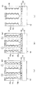
(第1実施形態)
図1は、本発明の第1実施形態に係る加速度センサ100の概略構成を示す図であり、(a)は加速度センサ100の概略平面図、(b)は(a)中のA−A一点鎖線に沿った概略断面図である。
(First embodiment)
FIG. 1 is a diagram showing a schematic configuration of an
[構成等]
図1(b)に示されるように、本加速度センサ100は、支持基板14上にシリコン半導体層12を積層してなる半導体基板10を備えている。
[Configuration]
As shown in FIG. 1B, the
本実施形態では、半導体基板10は、第1のシリコン半導体層11の上に絶縁層13を介して第2のシリコン半導体層12が積層されてなるSOI(シリコンオンインシュレータ)基板10として構成されている。
In the present embodiment, the
そして、この半導体基板10において、第1のシリコン半導体層11および絶縁層13が支持基板14として構成され、第2のシリコン半導体層12がシリコン半導体層12として構成されている。
In the
ここで、第1のシリコン半導体層11および第2のシリコン半導体層12は、単結晶シリコンまたはエピタキシャル成長ポリシリコンなどからなるものであり、絶縁層13は、シリコン酸化膜などからなる。
Here, the first
また、図1に示されるように、第2のシリコン半導体層12に対して半導体基板10の基板面と垂直な第1の方向Zにトレンチエッチングを行うことにより、第2のシリコン半導体層12にはトレンチ15が形成されている。
Further, as shown in FIG. 1, trench etching is performed on the second
そして、第2のシリコン半導体層12には、このトレンチ15によって区画された可動電極20、固定電極30がパターニング形成されている。固定電極30は、可動電極20に対して半導体基板10の基板面と平行な第2の方向Xにて検出間隔40を有して対向している。
In the second
なお、半導体基板10の基板面とは、半導体基板10の主面またはこれに平行な面であり、図1(a)中の紙面に相当する。さらに言うならば、第1の方向Zはいわゆる基板垂直方向、基板10の厚さ方向であり、第2の方向Xは基板面平行方向、基板10の厚さ方向と直交する方向である。
The substrate surface of the
本実施形態では、図1(a)に示されるように、可動電極20と固定電極30とは、互いにかみ合うように形成された櫛歯形状をなしており、この櫛歯における両電極20、30間の隙間が検出間隔40として構成されている。
In the present embodiment, as shown in FIG. 1A, the
そして、この検出間隔40においては、可動電極20は支持基板14すなわち絶縁層13から離間しており、固定電極30は支持基板14すなわち絶縁層13に接して支持されている。
In this
具体的には、可動電極20は櫛歯形状に配列された複数個のものからなる。そして、図1(a)に示されるように、複数個の可動電極20は連結部21によって一体的に連結されている。ここでは、連結部21は、可動電極20の配列方向に沿って延びる柱状をなすものであり、可動電極20と同様に、支持基板14から離間している。
Specifically, the
そして、この連結部21は、支持基板14に対してバネ性を有する梁部22を介して支持されている。この梁部22も可動電極20と同様に、支持基板14から離間しているが、一部はアンカー部24を介して支持基板14に支持されている。
And this
本例では、梁部21は、その一端部が柱状の連結部21の中間部に一体的に連結されており、他端部がアンカー部24を介して支持基板14に支持されている。アンカー部24は、固定電極30と同様に、第2のシリコン層12のうち支持基板14に接して固定された部分である。
In this example, one end of the
ここで、複数個の可動電極20のうち梁部22を中心にして梁部22の一方側(図1中の右側)に位置するものを第1の可動電極20a、他方側(図1中の左側)に位置するものを第2の可動電極20bとする。
Here, among the plurality of
さらに、連結部21のうち梁部22を中心として第1の可動電極20a側の端部には、可動電極20の変位を行うための錘部23が一体的に設けられている。この錘部23も、可動電極20と同様に、支持基板14から離間している。
Further, a
つまり、これら可動電極20、連結部21、梁部22および錘部23は一体化しており、これら一体化した各部20〜23は、上記トレンチ15により第2のシリコン半導体層12に区画形成された可動構造体20〜23として構成されている。
That is, the
そして、この可動構造体20〜23は、梁部22において上記アンカー部24に連結され、このアンカー部24を介して支持基板14から離間してリリースされた状態となっている。
The
このように支持基板14からリリースされた可動構造体20〜23は、トレンチエッチングにより形成されたトレンチ15を介して、可動構造体20〜23のパターンを形成した後、可動電極20を含む可動構造体20〜23における支持基板14側の底部をサイドエッチングすることによって、形成することができる。これらエッチングについての詳細は後述する。
In this way, the
なお、本実施形態では、固定電極30についても、支持基板14側の底部がサイドエッチングされるものの、固定電極30が支持基板14からリリースされる前にサイドエッチングを終了することにより、図1(b)に示されるように、固定電極30は支持基板14に接して支持されている。
In the present embodiment, the fixed
また、本実施形態では、図1(b)に示されるように、可動電極20における支持基板14側の底部は、支持基板14へ向かって狭くなるようなテーパ形状となっている。このような可動電極20のテーパ形状は、後述するサイドエッチングによって形成することができる。
In the present embodiment, as shown in FIG. 1B, the bottom of the
なお、当該サイドエッチングによって、支持基板14に接している固定電極30の底部もテーパ形状をなしている。また、このような可動電極20の底部は、このような鋭角的なテーパ形状以外にも、当該底部が支持基板14に向かって凸となった曲面形状すなわちラウンド形状となっていてもよい。
Note that the bottom portion of the fixed
そして、このように支持基板14からリリースされた複数個の可動電極20は、可動構造体20〜23全体として、図1(b)中の両矢印に示されるように、梁部22のバネ性により変位可能となっている。
The plurality of
つまり、可動電極20は、第1の方向Zに沿った加速度が印加されたときに、この第1の方向Zに変位できるようになっており、この変位によって、検出間隔40において対向する可動電極20と固定電極30との対向面積が変化する。
That is, the
より具体的に、本実施形態では、第1の方向Zに沿って連結部21の一端と他端とが互いに反対向きに変位する、言い換えれば、第1の可動電極20aと第2の可動電極20bとが互いに反対向きに変位するシーソー状の変位を行うものである。なお、梁部22は、このようなシーソー状の変位を行うようなバネ性を有するものであればよく、その形状は特に限定されるものではない。
More specifically, in the present embodiment, one end and the other end of the connecting
ここにおいて、本実施形態の加速度センサ100においては、図1(b)に示されるように、可動電極20における第2の方向Xに沿った幅が、固定電極30における第2の方向Xに沿った幅よりも小さく、可動電極20における第1の方向Zに沿った厚さが、固定電極30における第1の方向Zに沿った厚さよりも小さくなっている。
Here, in the
つまり、本実施形態では、基板面平行方向である第2の方向Xに沿った幅すなわち電極幅をみた場合、可動電極20の方が固定電極30よりも狭くなっており、第1の方向Zに沿った厚さすなわち基板垂直方向の電極厚さをみた場合、可動電極20の方が固定電極30よりも薄くなっている。
In other words, in the present embodiment, when the width along the second direction X that is the substrate surface parallel direction, that is, the electrode width is viewed, the
また、本実施形態では、複数個の可動電極20に応じて固定電極30も複数個存在するが、図1(a)に示されるように、各固定電極30は、第1の可動電極20aおよび第2の可動電極20b毎、あるいは、連結部21の上側と下側とで、それぞれ、固定電極用の連結部31によりまとめられている。
Further, in the present embodiment, there are a plurality of fixed
そして、図示しないが、各固定電極用の連結部31および可動構造体20〜23からは、それぞれ配線部が引き出されており、当該配線部の適所に設けられたパッドを介して、外部との電気的な接続が可能となっている。たとえば、当該パッドにワイヤボンディングを行うことにより、本加速度センサ100と外部回路との導通がなされる。
And although not shown in figure, the wiring part is each pulled out from the
[作動等]
次に、上記加速度センサ100の作動について述べる。
[Operation etc.]
Next, the operation of the
図2は、本加速度センサ100の第1の方向Zに沿った加速度の印加時における可動電極20の変位の様子を示すための概略断面図である。なお、図2中の破線は、可動電極20が変位する前すなわち加速度0の状態を示している。
FIG. 2 is a schematic cross-sectional view for illustrating a state of displacement of the
本実施形態の加速度センサ100は、基本的には、第1の方向Zに沿った加速度が印加されたときに可動電極20が第1の方向Zに変位し、この変位に伴う可動電極20と固定電極30との間の容量変化に基づいて加速度を検出するものである。
In the
上述したが、本実施形態では、上記加速度印加時に、梁部22のバネ性により第1の方向Zに沿って第1の可動電極20aと第2の可動電極20bとが互いに反対向きに変位するシーソー状の変位を行う。
As described above, in this embodiment, when the acceleration is applied, the first
図2においては、第1の方向Zに沿って上向きに加速度が印加され錘部23が加速度0のときよりも下がった状態、すなわち梁部22を基準として第1の可動電極20aの方が支持基板14に近づき、第2の可動電極20bの方が支持基板14から遠のいた状態を示している。以下、この状態を「錘の下方変位状態」という。
In FIG. 2, the acceleration is applied upward along the first direction Z and the
もちろん、図2中にて、第1の方向Zに沿って下向きに加速度が印加された場合には、図示の状態とは反対に、錘部23が加速度0のときよりも上がった状態、すなわち梁部22を基準として第1の可動電極20aの方が支持基板14から遠のき、第2の可動電極20bの方が支持基板14に近づいた状態となる。以下、この状態を「錘の上方変位状態」という。
Of course, in FIG. 2, when acceleration is applied downward along the first direction Z, contrary to the state shown in the figure, the
ここで、図2に示されるように、第1の可動電極20aと固定電極30との検出間隔15にて形成されている静電容量を第1の容量C1とし、第2の可動電極20bと固定電極30との検出間隔15にて形成されている静電容量を第2の容量C2とする。
Here, as shown in FIG. 2, the capacitance formed at the
上述したように、第1の方向Zに沿った加速度が印加されたときに、この第1の方向Zに沿って可動電極20が変位し、検出間隔15にて可動電極20と固定電極30との対向面積が変化するため、それに伴って、上記した第1の容量C1および第2の容量C1が変化する。このことについて、図3を参照して具体的に述べる。
As described above, when the acceleration along the first direction Z is applied, the
図3は、加速度と可動電極20の変位に伴う静電容量との関係を示す図である。この図3では、横軸に加速度、縦軸に静電容量を示している。
FIG. 3 is a diagram showing the relationship between the acceleration and the capacitance associated with the displacement of the
ここで、加速度は中央を0として、図3中の左側は、「錘の下方変位状態」となる加速度の向き、すなわち上記図2中の第1の方向Zに沿って上向きの加速度であり、図3中の右側は、「錘の上方変位状態」となる加速度の向き、すなわち上記図2中の第1の方向Zに沿って下向きの加速度である。 Here, the acceleration is assumed to be 0 at the center, and the left side in FIG. 3 is the direction of acceleration that becomes the “downward displacement state of the weight”, that is, the upward acceleration along the first direction Z in FIG. The right side in FIG. 3 is the direction of acceleration that becomes the “upward displacement state of the weight”, that is, the downward acceleration along the first direction Z in FIG.
そして、図3において、加速度は、0から左側に行くほど当該下向きの加速度が大きくなることを示しており、0から右側に行くほど当該上向きの加速度が大きくなることを示している。 In FIG. 3, the acceleration indicates that the downward acceleration increases from 0 to the left side, and the upward acceleration increases from 0 to the right side.
図3に示されるように、本実施形態では、可動電極20の変位に伴い、各静電容量C1、C2は非線形に変化する。これは、主として、第1の方向Zに沿った電極厚さにおいて可動電極20の方が固定電極30よりも薄くなっているため、可動電極20が支持基板14に近づく方向に変位しても、対向面積はさほど変化せず、遠ざかる方向に変位すると対向面積が減少することによる。
As shown in FIG. 3, in the present embodiment, the capacitances C <b> 1 and C <b> 2 change nonlinearly with the displacement of the
そして、本加速度センサ100では、可動電極20の変位に伴うこれら各容量C1、C2の容量差(C2−C1)の変化に基づいて加速度の検出を行うようにしている。
In the
図3に示されるように、各静電容量C1、C2は非線形に変化するが、差分(C2−C1)はほぼ直線性を持つ。そのため、本実施形態では、この容量差(C2−C1)を計測することにより、直線性のよい感度が得られる。以上が、本実施形態における加速度検出動作である。 As shown in FIG. 3, the capacitances C1 and C2 change nonlinearly, but the difference (C2−C1) has almost linearity. Therefore, in this embodiment, sensitivity with good linearity can be obtained by measuring this capacity difference (C2-C1). The above is the acceleration detection operation in the present embodiment.
[製造方法等]
次に、本実施形態の加速度センサ100の製造方法について、図4(a)〜(e)、図5(a)〜(c)を参照して述べる。図4は、本製造方法におけるトレンチ形成工程を示す断面図であり、図5はリリース工程を示す断面図である。
[Manufacturing method]
Next, a method for manufacturing the
まず、支持基板14上にシリコン半導体層12を積層してなる半導体基板10を用意する。本実施形態では、半導体基板10として、第1のシリコン半導体層11の上に絶縁層13を介して第2のシリコン半導体層12が積層され、第1のシリコン半導体層11および絶縁層13が支持基板14、第2のシリコン半導体層12がシリコン半導体層として構成されているSOI基板10を用意する。
First, the
次に、図4(a)に示されるように、第2のシリコン半導体層12の表面側に所定パターンのマスクM1を形成する(マスク形成工程)。このマスクM1は、光硬化型樹脂や熱硬化型樹脂等からなるレジスト材料を用い、フォトリソグラフ技術等を駆使することにより形成することができる。 Next, as shown in FIG. 4A, a mask M1 having a predetermined pattern is formed on the surface side of the second silicon semiconductor layer 12 (mask forming step). The mask M1 can be formed by using a resist material made of a photocurable resin, a thermosetting resin, or the like and making full use of a photolithographic technique or the like.
そして、このマスクM1は、上記トレンチ15となる部位に開口部を有するパターンのマスクM1として形成される。つまり、第2のシリコン半導体層12のうちマスクM1でマスキングされた部位は、可動構造体20〜23、アンカー部24および固定電極30のパターンとなっている。
The mask M1 is formed as a mask M1 having a pattern having an opening at a portion to be the
次に行うトレンチ形成工程およびリリース工程は、真空チャンバー内にSOI基板10を設置し、反応性ガスを導入してプラズマ化させた状態で行う反応性イオンエッチング(Reactive Ion Etching、RIE)によって行われ、しかも、エッチングと同時もしくは時間切り替えにより、トレンチ15の側壁に当該側壁を保護する側壁保護膜を形成する工程として行うものである。
The trench formation process and the release process to be performed next are performed by reactive ion etching (RIE) performed by placing the
図4に示されるトレンチ形成工程は、エッチング性ガスのプラズマにより第2のシリコン半導体層12をエッチングするエッチングステップと、堆積性ガスのプラズマにより側壁保護膜15aを形成する保護膜形成ステップとを、切り替えながら交互に繰り返すことによってなされるものである。
The trench formation process shown in FIG. 4 includes an etching step for etching the second
まず、図4(a)では、最初のエッチングステップが示されている。まず、真空チャンバー内に、上記マスクM1が形成されたSOI基板10を設置する。そして、この真空チャンバー内に、エッチング性ガスとしてシリコンエッチングを行うためのSF6ガスを、所定時間(例えば、7秒間程度)導入する。
First, in FIG. 4A, the first etching step is shown. First, the
これにより、第2のシリコン半導体層12がエッチングされ、第2のシリコン半導体層12の表面から絶縁層13に到達するトレンチ15が部分的に形成される。このとき、SF6ガスは電界中にてプラズマとなって、エッチングに寄与する。図4(a)では、SF6ガスはプラスイオンの形で表されている。
Thereby, the second
そして、SOI基板10にはバイアス電力(バイアスパワー)を印加することにより、このイオンをSOI基板10の方向に引きつけ、SOI基板10の基板面と垂直な第1の方向Zへの異方性のトレンチエッチングを実行するようにしている。
Then, by applying bias power (bias power) to the
次に、図4(b)に示されるように、最初の保護膜形成ステップを行う。すなわち、エッチング性ガスであるSF6ガスの導入を停止し、真空チャンバー内に、堆積性ガスとしてC4F8ガスを所定時間(例えば、5秒間程度)導入する。 Next, as shown in FIG. 4B, an initial protective film formation step is performed. That is, the introduction of SF 6 gas, which is an etching gas, is stopped, and C 4 F 8 gas as a deposition gas is introduced into the vacuum chamber for a predetermined time (eg, about 5 seconds).
この保護膜形成ステップにおいては、SOI基板10には、バイアス電力を印加しない。それにより、トレンチ15の側壁および底部に均一に側壁保護膜15aが形成される。ここでC4F8ガス等のフッ素系ガスを採用した場合には、側壁保護膜15aはフッ化物ポリマーからなるものになる。
In this protective film forming step, bias power is not applied to the
続いて、図4(c)、(d)に示されるように、エッチングステップと保護膜形成ステップとを、切り替えながら交互に繰り返して行う。ここで、1回のエッチングステップによるエッチング深さは、例えば、0.1〜0.5μm程度にできる。 Subsequently, as shown in FIGS. 4C and 4D, the etching step and the protective film forming step are alternately repeated while switching. Here, the etching depth by one etching step can be set to about 0.1 to 0.5 μm, for example.
そして、最終的に、図4(e)に示されるように、第2のシリコン半導体層12の表面から絶縁層13に到達するトレンチ15が完成する。ここまでが、トレンチ形成工程である。
Finally, as shown in FIG. 4E, a
このように、トレンチ形成工程では、第2のシリコン半導体層12に対してSOI基板10の基板面と垂直な第1の方向Zにトレンチエッチングを行うことにより、第2のシリコン半導体層12に、可動電極20を含む上記可動構造体20〜23、アンカー部24および固定電極30のパターンを形成する。
As described above, in the trench formation step, the second
ここまでが、本実施形態のトレンチ形成工程の概要であるが、ここで、本実施形態では、可動電極20における第2の方向Xに沿った電極幅が固定電極30における第2の方向Xに沿った電極幅よりも小さくなるように、可動電極20と固定電極30とのパターンを形成する。
Up to here is the outline of the trench formation process of the present embodiment. Here, in the present embodiment, the electrode width along the second direction X in the
このことは、上記のマスク形成工程におけるマスクM1のマスクパターンにより用意に実現できる。そして、このようにしてトレンチ形成工程を行った後、続いて、図5に示されるリリース工程を行う。 This can be easily realized by the mask pattern of the mask M1 in the mask forming process. And after performing a trench formation process in this way, the release process shown by FIG. 5 is performed continuously.
このリリース工程は、たとえば、上述したトレンチ形成工程と同一のエッチング条件によって、エッチングを継続することにより、行うことができる。つまり、本実施形態でも、上記のエッチングステップと保護膜形成ステップとの繰り返しを行うことにより、リリース工程を行うことができる。 This release process can be performed, for example, by continuing the etching under the same etching conditions as the trench forming process described above. That is, also in this embodiment, the release process can be performed by repeating the etching step and the protective film forming step.
図5(a)に示されるように、トレンチ15の形成後に継続して導入されるエッチング性ガスのプラスイオンによって、本例ではシリコン酸化膜からなる絶縁層13は、プラスの状態に帯電している。
As shown in FIG. 5A, the insulating
そこへ、さらに、エッチング性ガスのプラスイオンが導入されるが、図5(a)に示されるように、トレンチ15の底部において、このプラスイオンは、プラスに帯電した絶縁層13と反発しあって、横方向へ拡散する。
Further, positive ions of the etching gas are further introduced. As shown in FIG. 5A, the positive ions repel the positively charged insulating
すると、図5(a)に示されるように、トレンチ15の底部において、第2のシリコン半導体層12における支持基板14側の底部が横方向にエッチングされ、すなわちサイドエッチングされ、第2のシリコン半導体層12にノッチ15bが形成される。
Then, as shown in FIG. 5A, at the bottom of the
ここで、この横方向のエッチングすなわちサイドエッチングにおいては、エッチング性ガスは、保護膜形成ステップにて形成された側壁保護膜15aを、エッチングもしくは物理的にスパッタなどによって除去しながら、第2のシリコン半導体層12をエッチングしていく。
Here, in this lateral etching, that is, side etching, the etching gas removes the sidewall
そして、このサイドエッチングを継続していくことによって、図5(b)に示されるように、ノッチ15bが拡大していき、やがて、図5(c)に示されるように、第2のシリコン半導体層12が絶縁層13からリリースされた部分としての可動構造体20〜23ができあがる。
Then, by continuing this side etching, the
図5(c)に示される例では、2つのノッチ15b同士が連通するとともに、ノッチ15bの形状の一部が、可動電極20の底部に残ることにより、上記したテーパ形状をなす可動電極20の底部を実現することができる。
In the example shown in FIG. 5C, the two
ここで、本実施形態では、サイドエッチングのとき、可動電極20の方が固定電極30よりも電極幅が狭いため、電極幅の狭い可動電極20の方が、電極幅の広い固定電極30よりも下地である支持基板14からのリリースが早く完了する。
Here, in this embodiment, at the time of side etching, the
そのため、固定電極30が支持基板14からリリースされる前であって、かつに可動電極20における支持基板14側の底部が上記テーパ形状となったときに、サイドエッチングを終了することができる。そして、その結果、第1の方向Zに沿った電極厚さを、可動電極20の方が固定電極30よりも小さい構成となる。
Therefore, the side etching can be finished before the fixed
このように、リリース工程では、トレンチエッチングにより形成されたトレンチ15を介して、可動電極20および固定電極30における支持基板14側の底部をサイドエッチングすることによって、可動電極20を支持基板14からリリースする。こうして、本実施形態の加速度センサ100が完成する。
Thus, in the release step, the
[効果等]
以上述べてきたように、本実施形態における加速度センサ100は、支持基板14上にシリコン半導体層12を積層してなる半導体基板10を備え、シリコン半導体層12に対して半導体基板10の基板面と垂直な第1の方向Zにトレンチエッチングを行うことにより、シリコン半導体層12には、可動電極20と、可動電極20に対して半導体基板10の基板面と平行な第2の方向Xにて検出間隔40を有して対向する固定電極30とがパターニングされており、第1の方向Zに沿った加速度が印加されたときに可動電極20が第1の方向Zに変位し、この変位に伴う可動電極20と固定電極30との間の容量変化に基づいて加速度を検出するようにした垂直変位型の加速度センサであることを基本構成としている。
[Effects]
As described above, the
そして、このような基本構成を有する本加速度センサ100は、次のような独自の特徴点を有する。
And this
・トレンチエッチングにより形成されたトレンチ15を介して、可動電極20および固定電極30における支持基板14側の底部をサイドエッチングすることによって、可動電極20が支持基板14からリリースされていること。
The
・可動電極20における第2の方向Xに沿った幅が、固定電極30における第2の方向Xに沿った幅よりも小さく、可動電極20における第1の方向Zに沿った厚さが、固定電極30における第1の方向Zに沿った厚さよりも小さいこと。本実施形態によれば、このような特徴点を有する垂直変位型の加速度センサ100が提供される。
The width of the
上述したように、従来では、可動電極と固定電極とのトレンチエッチングによるパターニングの際にRIEラグを利用するため、可動電極と固定電極とで基板垂直方向の厚さの出来映えがばらついていた。 As described above, conventionally, since the RIE lug is used for patterning of the movable electrode and the fixed electrode by trench etching, the thickness of the movable electrode and the fixed electrode varies in the vertical direction of the substrate.
それに対して、本実施形態では、エッチングにより残る残り部の幅を、可動電極20と固定電極30とで変えることにより、可動電極20および固定電極30のトレンチエッチングによるパターニングおよび引き続くサイドエッチングによる可動電極20のリリースを行うことができる。
On the other hand, in the present embodiment, the width of the remaining portion remaining after etching is changed between the
エッチングでは、上記残り部の幅が狭ければ、当該残り部を下地からリリースするための底部のサイドエッチングが早く完了し、上記残り部が広ければ、その底部のサイドエッチングの完了は遅くなる。このことは、エッチング対象物の物理的な大小により決まってくることであるため、エッチングレートの差いわゆるRIEラグを利用した場合に比べて制御性に優れる。 In the etching, if the width of the remaining portion is narrow, the side etching of the bottom portion for releasing the remaining portion from the base is completed early, and if the remaining portion is wide, the completion of the side etching of the bottom portion is delayed. This is determined by the physical size of the object to be etched, so that the controllability is excellent as compared with the case where a difference in etching rate, that is, a RIE lag is used.
つまり、本実施形態では、上述したように、第2の方向Xすなわち基板面平行方向に沿った幅を、可動電極20の方が固定電極30よりも小さくするように、可動電極20および固定電極30のトレンチエッチングによるパターニングを行い、引き続いて、両電極20、30の底部のサイドエッチングを行い、可動電極20をリリースする。
That is, in the present embodiment, as described above, the
そして、このサイドエッチングのとき、残り部としては、可動電極20の方が固定電極30よりも幅が狭くなっているため、幅の狭い可動電極20の方が、幅の広い固定電極30よりも下地である支持基板14からのリリースが早く完了する。その結果、第1の方向Zに沿った厚さすなわち基板垂直方向の厚さを、可動電極20の方が固定電極30よりも小さい構成を実現することができる。
In this side etching, the remaining portion of the
このように、本実施形態では、このサイドエッチングの出来映えが残り部の幅によって制御される結果、可動電極20と固定電極30とで第1の方向Zすなわち基板垂直方向の厚さが異なる構成について、再現性のばらつきが少なく安定した出来映えを実現することができる。
As described above, in the present embodiment, as a result of the side etching performance being controlled by the width of the remaining portion, the
したがって、本実施形態によれば、支持基板14上に積層されたシリコン半導体層12に、トレンチエッチングにより可動電極20および固定電極30をパターニング形成し、基板垂直方向に加速度が印加されたときの可動電極20と固定電極30との容量変化に基づいて加速度検出を行うようにした垂直変位型の加速度センサ100において、可動電極20および固定電極30の安定した出来映えを実現することができる。
Therefore, according to this embodiment, the
ここで、トレンチエッチングによる残り部としての可動電極20や固定電極30の電極幅を変えることにより、引き続き行うサイドエッチングによって、可動電極20や固定電極30の電極厚さを精度良く制御できることについて、より具体的に述べておく。
Here, by changing the electrode width of the
図6は、電極幅および電極厚さの異なる複数個の電極構造体Dがトレンチ15を介して配列された構成を示す概略断面図である。この図6では、各電極構造体Dは、本加速度センサ100における可動電極20や固定電極30に相当するものである。
FIG. 6 is a schematic cross-sectional view showing a configuration in which a plurality of electrode structures D having different electrode widths and electrode thicknesses are arranged via
そして、図6では、隣り合う電極構造体Dにおける第2の方向Xに沿った電極間隔WSを一定とし、各電極構造体Dにおける第2の方向Xに沿った電極幅WLを左側のものから右側のものにいくほど広いものとしている。 In FIG. 6, the electrode spacing WS along the second direction X in the adjacent electrode structures D is constant, and the electrode width WL along the second direction X in each electrode structure D is from the left side. It is made wider as it goes to the right side.
そして、この図6に示される構成は、上記製造方法に準じたトレンチエッチングを行うことにより、このように電極幅WLの異なる複数個の電極構造体Dのパターンを形成した後、上記同様のトレンチ15を介したサイドエッチングを行った結果として、得られたものである。 Then, the structure shown in FIG. 6 is formed by performing trench etching according to the above manufacturing method, thus forming a pattern of a plurality of electrode structures D having different electrode widths WL, and then performing the same trench as described above. As a result of performing side etching through 15.
図6に示されるように、このサイドエッチングのとき、複数個の電極構造体Dにおいて、電極幅の狭いものほど、支持基板14からのリリースが早く完了するため、第1の方向Zに沿った電極厚さが薄くなっている。図6では、電極構造体Dの底部と支持基板14との距離をギャップhとして示してあるが、電極幅の狭い電極構造体Dほど、このギャップhが高くなっている。
As shown in FIG. 6, in this side etching, in the plurality of electrode structures D, as the electrode width is narrower, the release from the
そして、この電極構造体Dの電極厚さを反映する上記ギャップhを利用して、上記電極間隔WSを一定としたときの上記電極幅WLとギャップhとの関係を調査した。その結果を図7に示す。 Then, using the gap h reflecting the electrode thickness of the electrode structure D, the relationship between the electrode width WL and the gap h when the electrode interval WS was made constant was investigated. The result is shown in FIG.
図7に示されるように、電極間隔WSを一定として電極幅WLを増加させていくと、ギャップhは単調減少する傾向にあることが確認された。逆に言えば、電極間隔WSを一定として電極幅WLを増加させていくと、電極厚さは単調増加する傾向にあることがわかった。 As shown in FIG. 7, it was confirmed that when the electrode width WL was increased while the electrode interval WS was constant, the gap h tended to monotonously decrease. In other words, it has been found that the electrode thickness tends to monotonously increase when the electrode width WL is increased while the electrode interval WS is constant.
つまり、電極幅WLとギャップhとの関係、すなわち、電極幅WLと電極厚さとの関係は、ほぼ直線的な比例関係にあることがわかった。それゆえ、可動電極20において、電極幅WLを変えてやれば、サイドエッチングによって狙いの電極厚さを実現することは容易である。
That is, it has been found that the relationship between the electrode width WL and the gap h, that is, the relationship between the electrode width WL and the electrode thickness is in a substantially linear proportional relationship. Therefore, if the electrode width WL is changed in the
たとえば、図7において、電極幅WLがW1のものとそれよりも広いW2のものとにおいて、サイドエッチング後のギャップhは、前者がh1、後者がそれよりも大きいh2であり、両者の底部側における段差は(h2−h1)となる。このことを可動電極20と固定電極30とに応用してやれば、両電極20、30の電極幅WLを調整することで、両電極20、30の電極厚さにおいて所望の値を得ることができる。
For example, in FIG. 7, when the electrode width WL is W1 and W2 wider than that, the gap h after side etching is h1 for the former and h2 larger for the latter, and the bottom side of both The step in is (h2-h1). If this is applied to the
このように、可動電極20や固定電極30の電極幅を変えることによってサイドエッチングによる電極厚さを制御することは、従来のような電極間隔を変えRIEラグを利用することによって電極厚さを制御する場合に比べて、再現性よく行うことができ、ばらつきが少ないものとなる。
In this way, controlling the electrode thickness by side etching by changing the electrode width of the
また、本実施形態の加速度センサ100においては、検出間隔40では、可動電極20は支持基板14から離間しているが、固定電極30は支持基板14に接して支持されていることも特徴のひとつである。
In the
また、本実施形態の加速度センサ100では、半導体基板10として、第1のシリコン半導体層11の上に絶縁層13が積層されてなる支持基板14の上に、シリコン半導体層としての第2のシリコン半導体層12が積層されてなるSOI基板10を採用したことも、特徴のひとつである。
In the
また、本実施形態では、可動電極20と固定電極30とは、互いにかみ合うように形成された櫛歯形状をなしており、この櫛歯における隙間が検出間隔40として構成されていることも特徴のひとつである。
Further, in the present embodiment, the
さらに、本実施形態の加速度センサ100においては、可動電極20における支持基板14側の底部は、支持基板14へ向かって狭くなるようなテーパ形状もしくはラウンド形状となっていることも特徴のひとつである。
Furthermore, in the
可動電極20が第1の方向Zへ変位するときに、可動電極20とその下地の支持基板14との間でダンピングが生じる可能性があるが、このようにすれば、可動電極20の底部の空気流れを良くして空気抵抗を小さくできるため、ダンピングを適切に抑制することができる。その結果、高い周波数領域の加速度であっても、感度を十分に確保できるという利点がある。
When the
また、過大な衝撃が加わったとき可動電極20が第1の方向Zへ大きく変位して可動電極20の底部と支持基板14とが接触して付着すること、いわゆるスティッキングが発生する可能性があるが、支持基板14に対向する可動電極20の底部の対向面積を小さくできるため、そのようなスティッキングを極力抑制でき、好ましい。
Further, when an excessive impact is applied, the
また、本実施形態では、複数個の可動電極20を連結する連結部21は、支持基板14に対してバネ性を有する梁部22を介して支持されており、複数個の可動電極20においては、梁部22を中心にして一方側の第1の可動電極20aと他方側の第2の可動電極20bとが、梁部22のバネ性により第1の方向Zに沿って互いに反対向きに変位するシーソー状の変位を行うものとなっていることも特徴のひとつである。
Further, in the present embodiment, the connecting
それによれば、このシーソー状変位に伴う第1の可動電極20aと固定電極30との間の容量C1と、第2の可動電極20bと固定電極30との容量C2との容量差(C2−C1)の変化に基づいて加速度の検出を行うことができ、上記図3に示されるように、直線性のよい感度を得ることができる。
According to this, a capacitance difference (C2−C1) between the capacitance C1 between the first
さらに、本実施形態の加速度センサ100によれば、連結部21のうち梁部22を中心として一方側の部位に、シーソー状の変位を行うための錘部23が設けられていることも特徴のひとつである。そして、それによれば、錘部23の重さによって、上記シーソー状の変位を適切に実現することができる。
Furthermore, according to the
また、本実施形態の加速度センサ100においては、シリコン半導体層12および支持基板14が、単結晶シリコンまたはエピタキシャル成長ポリシリコンからなるものであることも特徴のひとつである。
In addition, the
また、本実施形態によれば、上記図1に示される本加速度センサ100を適切に製造することの可能な加速度センサの製造方法として、次のような特徴点を有する製造方法が提供される。
Moreover, according to this embodiment, the manufacturing method which has the following characteristic points is provided as a manufacturing method of the acceleration sensor which can manufacture this
・支持基板14上にシリコン半導体層12を積層してなる半導体基板10を用意し、シリコン半導体層12に対して半導体基板10の基板面と垂直な第1の方向Zにトレンチエッチングを行うことにより、シリコン半導体層12に、可動電極20と、可動電極20に対して半導体基板10の基板面と平行な第2の方向Xにて検出間隔40を有して対向する固定電極30とのパターンを形成するトレンチ形成工程を備えること。
By preparing the
・前記トレンチ形成工程では、可動電極20における第2の方向Xに沿った幅が固定電極30における第2の方向Xに沿った幅よりも小さくなるように、可動電極20と固定電極30とのパターンを形成すること。
In the trench formation step, the
・上記トレンチエッチングにより形成されたトレンチ15を介して、可動電極20および固定電極30における支持基板14側の底部をサイドエッチングすることによって、可動電極20を支持基板14からリリースするリリース工程を備えること。
A release step of releasing the
これらの点を特徴とする本実施形態の加速度センサの製造方法によれば、上述したように、トレンチ形成工程にて、第2の方向Xすなわち基板面平行方向に沿った幅を、可動電極20の方が固定電極30よりも小さくするように、可動電極20および固定電極30のトレンチエッチングによるパターニングを行い、引き続いて、リリース工程にて、両電極20、30の底部のサイドエッチングを行い、可動電極20をリリースすることで、本加速度センサ100を製造できる。
According to the acceleration sensor manufacturing method of this embodiment characterized by these points, as described above, in the trench formation step, the width along the second direction X, that is, the substrate surface parallel direction, is set to the
そして、このサイドエッチングのとき、電極幅の狭い可動電極20の方が、電極幅の広い固定電極30よりも下地である支持基板14からのリリースが早く完了するため、基板垂直方向である第1の方向Zに沿った電極厚さを、可動電極20の方が固定電極30よりも小さい構成とすることができる。
In this side etching, the
ここで、上述したように、トレンチエッチングによる残り部として幅が狭い部位である可動電極20の方が、幅が広い部位である固定電極30よりも、リリースが早く完了することは、エッチング対象物の物理的な大小により決まってくることであるため、RIEラグを利用した場合に比べて制御性に優れる。
Here, as described above, the
そのため、本実施形態の製造方法によっても、垂直変位型の加速度センサ100において、可動電極20および固定電極30の安定した出来映えを実現することができる。
Therefore, even with the manufacturing method of the present embodiment, it is possible to achieve a stable workmanship of the
ここで、本実施形態の製造方法においては、リリース工程は、検出間隔40において、可動電極20は支持基板14からリリースさせるとともに、固定電極30は支持基板14からリリースさせないように、サイドエッチングを完了させるものであることも特徴のひとつである。
Here, in the manufacturing method of this embodiment, in the release step, the side etching is completed so that the
それによれば、できあがった加速度センサにおいて、検出間隔40では可動電極20は支持基板14から離間し、固定電極30は支持基板14に接して支持されている状態を適切に形成することができる。
Accordingly, in the completed acceleration sensor, it is possible to appropriately form a state in which the
(第2実施形態)
図8は、本発明の第2実施形態に係る加速度センサ200の概略構成を示す図であり、(a)は加速度センサ200の概略平面図、(b)は(a)中のB−B一点鎖線に沿った概略断面図である。
(Second Embodiment)
FIG. 8 is a diagram showing a schematic configuration of an
図8に示されるように、本実施形態における加速度センサ200も、支持基板14上にシリコン半導体層12を積層してなる半導体基板10を備え、シリコン半導体層12に対して第1の方向Zにトレンチエッチングを行うことにより、シリコン半導体層12には、可動電極20と固定電極30とがパターニングされており、第1の方向Zに沿った加速度が印加されたときに可動電極20が第1の方向Zに変位し、この変位に伴う両電極20と30との間の容量変化に基づいて加速度を検出するようにした垂直変位型の加速度センサであることを基本構成としている。
As shown in FIG. 8, the
そして、本加速度センサ200も、上記実施形態と同様、トレンチ15を介した上記サイドエッチングによって可動電極20が支持基板14からリリースされていること、および、可動電極20における第2の方向Xに沿った幅および第1の方向Zに沿った厚さが、固定電極30におけるそれらよりも小さいことを特徴としている。
In the
そのため、上記実施形態と同様、本実施形態によっても、支持基板14上に積層されたシリコン半導体層12に、トレンチエッチングにより可動電極20および固定電極30をパターニング形成し、基板垂直方向に加速度が印加されたときの可動電極20と固定電極30との容量変化に基づいて加速度検出を行うようにした垂直変位型の加速度センサ200において、可動電極20および固定電極30の安定した出来映えを実現することができる。
Therefore, as in the above-described embodiment, according to this embodiment, the
また、本実施形態の加速度センサ200においても、複数個の可動電極20を連結する連結部21は、支持基板14に梁部22を介して支持されており、複数個の可動電極20においては、梁部22を中心にして一方側の第1の可動電極20aと他方側の第2の可動電極20bとが、梁部22のバネ性により第1の方向Zに沿って互いに反対向きに変位するシーソー状の変位を行うものとなっており、上記容量差(C2−C1)の変化に基づいて加速度の検出を行うようになっている。
Also in the
このようなシーソー状の変位を行う構成の場合、連結部21における梁部22の一方側に錘部23を設けると、この錘部23とその周囲の固定電極30との間で静電容量が形成される場合がある。
In the case where the seesaw-like displacement is performed, if a
すると、この錘部23により形成された静電容量分、梁部22を中心として一方側と他方側、すなわち第1の可動電極20a側と第2の可動電極20b側とで、静電容量のアンバランスが生じる。
Then, the capacitance of the capacitance formed by the
たとえば、上記図1に示される加速度センサ100の場合、第1の可動電極20a側に設けられた錘部23と、その隣の固定電極30との間で静電容量部が形成されるため、梁部22を中心として第1の可動電極20a側の方が反対側の第2の可動電極20b側よりも、錘部23の静電容量部の分、静電容量部の数が多くなる。ただし、錘部23とその隣の固定電極30との間隔は、図1からもわかるように、可動電極20と固定電極30との検出間隔40よりも少し広めにとってある。
For example, in the case of the
そのため、加速度検出時において、上記容量差(C2−C1)をとるとき、回路側の処理が複雑になるなど、好ましくない。つまり、シーソー状の変位を行う垂直変位型の加速度センサの場合、第1の可動電極20a側の静電容量部と第2の可動電極20b側の静電容量部とは、同数であることが好ましい。
Therefore, when the acceleration is detected, taking the capacitance difference (C2-C1) is not preferable because the processing on the circuit side becomes complicated. That is, in the case of a vertical displacement type acceleration sensor that performs a seesaw-like displacement, the number of capacitance parts on the first
このような問題に対して、図8に示されるように、本実施形態の加速度センサ200においては、連結部21のうち梁部22を中心として錘部23が設けられている方の部位とは反対側の部位、すなわち連結部21における第2の可動電極側の端部には、錘部23により形成された静電容量分を補償するための容量補償部50が形成されている。
For such a problem, as shown in FIG. 8, in the
ここで、容量補償部50は、可動構造体20〜23の一部としてこれと一体的に形成されたものであるが、錘部23よりも大幅に軽いものであり錘部23による変位を実質的に阻害しないような質量のものとする。
Here, the
また、この容量補償部50とその隣の固定電極30との間隔は、上記した錘部23とその隣の固定電極30との間隔と同程度とし、この容量補償部50による静電容量が、錘部23による静電容量と同程度になるようにする。
In addition, the distance between the
このように容量補償部50を設けることにより、この容量補償部50とその隣の固定電極30との間で静電容量部が形成されるため、梁部22を中心として第1の可動電極20a側と第2の可動電極20b側とで、静電容量部の数を同じにできる。
By providing the
このように、本実施形態によれば、シーソー状の変位を行う加速度センサ200において、錘部23に起因する第1の可動電極20a側と第2の可動電極20b側との間の静電容量のアンバランスを補正することができるため、加速度検出時において、上記容量差(C2−C1)による検出が容易になる。
Thus, according to this embodiment, in the
以上、本実施形態では、上記第1実施形態の加速度センサに対して容量補償部50を付与したものであり、それ以外の部分は同一である。そのため、本実施形態にて改めて述べたこと以外にも、本実施形態の加速度センサ200によれば、上記第1実施形態と同様の作用効果を奏することはもちろんである。
As described above, in the present embodiment, the
(他の実施形態)
なお、上記実施形態においては、可動電極20における支持基板14側の底部は、支持基板14へ向かって狭くなるようなテーパ形状もしくはラウンド形状となっていたが、当該底部は、そのようなテーパもしくはラウンド形状でなくてもよく、たとえば、図9に示されるように、ストレート形状であってもよい。
(Other embodiments)
In the above embodiment, the bottom of the
また、図10は、もうひとつの他の実施形態としての加速度センサの概略断面図である。上記実施形態の加速度センサにおいては、検出間隔40では、可動電極20は支持基板14から離間しているが、固定電極30は支持基板14に接して支持されていた。
FIG. 10 is a schematic sectional view of an acceleration sensor as another embodiment. In the acceleration sensor of the above embodiment, the
それに対して、図10に示されるように、固定電極30も支持基板からリリースされ離間していてもよい。なお、これら図9、図10に示される加速度センサの構成は、各電極20、30の電極幅やサイドエッチングのタイミングを調整することにより、形成することができる。
On the other hand, as shown in FIG. 10, the fixed
また、上記実施形態では、可動電極20は、連結部21の中間部に梁部22が連結されているため、上記したシーソー状の変位を行うものであったが、可動電極の変位形態はこれに限定されない。たとえば梁部のバネ特性を変更してすべての可動電極20が第1の方向Zに平行に変位するものであってもよい。
Further, in the above embodiment, the
また、半導体基板としては、上記SOI基板に限定されるものではなく、支持基板上にシリコン半導体層を積層してなるものであればよい。 Further, the semiconductor substrate is not limited to the SOI substrate, and any semiconductor substrate may be used as long as a silicon semiconductor layer is stacked on a supporting substrate.
また、半導体基板のシリコン半導体層に形成される可動電極や固定電極の構成は、上記櫛歯形状に限定されるものではない。つまり、可動電極は、半導体基板の支持基板からリリースされており、半導体基板の基板面と垂直な第1の方向Zに沿った加速度が印加されたときに、この第1の方向Zに変位するものであればよい。 In addition, the configuration of the movable electrode and the fixed electrode formed on the silicon semiconductor layer of the semiconductor substrate is not limited to the comb shape. That is, the movable electrode is released from the support substrate of the semiconductor substrate, and is displaced in the first direction Z when an acceleration along the first direction Z perpendicular to the substrate surface of the semiconductor substrate is applied. Anything is acceptable.
また、固定電極は、可動電極に対して半導体基板の基板面と平行な第2の方向Xにて検出間隔を有して対向するものであって、上記加速度印加時に変位せず支持基板に固定されたものであればよい。 The fixed electrode is opposed to the movable electrode with a detection interval in a second direction X parallel to the substrate surface of the semiconductor substrate, and is fixed to the support substrate without being displaced when the acceleration is applied. If it was done.
要するに、本発明は、支持基板上にシリコン半導体層を積層してなる半導体基板を備え、シリコン半導体層に対して基板垂直方向である第1の方向にトレンチエッチングを行うことにより、シリコン半導体層には、可動電極と、可動電極に対して基板面平行方向である第2の方向にて検出間隔を有して対向する固定電極とがパターニングされており、加速度印加時における可動電極の第1の方向への変位に伴う可動電極と固定電極との間の容量変化に基づいて加速度を検出するようにした垂直変位型の加速度センサであるならば、適用可能なものである。 In short, the present invention includes a semiconductor substrate in which a silicon semiconductor layer is stacked on a support substrate, and trench etching is performed in a first direction that is perpendicular to the silicon semiconductor layer, thereby forming a silicon semiconductor layer. Are patterned with a movable electrode and a fixed electrode facing the movable electrode with a detection interval in a second direction that is parallel to the substrate surface. Any vertical displacement type acceleration sensor that detects acceleration based on a change in capacitance between a movable electrode and a fixed electrode accompanying displacement in a direction is applicable.
そして、本発明は、このような加速度センサにおいて、トレンチエッチングにより形成されたトレンチを介して、可動電極および固定電極における支持基板側の底部をサイドエッチングすることによって、可動電極が支持基板からリリースしているとともに、可動電極20における第2の方向Xに沿った幅が固定電極30における同幅よりも小さく、可動電極20における第1の方向Zに沿った厚さが固定電極30における同厚さよりも小さいことを要部とし、さらには、そのような加速度センサを適切に製造する上記製造方法を提供するものである。
In the acceleration sensor as described above, the movable electrode is released from the support substrate by side-etching the bottom of the movable electrode and the fixed electrode on the support substrate side through the trench formed by the trench etching. In addition, the width of the
また、本発明の垂直変位型の加速度センサと同一チップ上に本発明で述べた製造方法を用いて、平行変位型の加速度センサを配置することも当然可能であるため、3軸の加速度センサを容易に実現可能である。 It is also possible to arrange a parallel displacement acceleration sensor on the same chip as the vertical displacement acceleration sensor of the present invention by using the manufacturing method described in the present invention. It can be easily realized.
10…半導体基板としてのSOI(シリコンオンインシュレータ)基板、
11…第1のシリコン半導体層、12…第2のシリコン半導体層、13…絶縁層、
14…支持基板、15…トレンチ、20…可動電極、20a…第1の可動電極、
20b…第2の可動電極、21…連結部、22…梁部、23…錘部、
30…固定電極、40…検出間隔、50…容量補償部、
X…第2の方向、Z…第1の方向。
10 ... SOI (silicon on insulator) substrate as a semiconductor substrate,
DESCRIPTION OF
14 ... support substrate, 15 ... trench, 20 ... movable electrode, 20a ... first movable electrode,
20b ... second movable electrode, 21 ... connecting portion, 22 ... beam portion, 23 ... weight portion,
30 ... Fixed electrode, 40 ... Detection interval, 50 ... Capacitance compensator,
X: second direction, Z: first direction.
Claims (13)
前記シリコン半導体層(12)に対して前記半導体基板(10)の基板面と垂直な第1の方向(Z)にトレンチエッチングを行うことにより、前記シリコン半導体層(12)には、可動電極(20)と、前記可動電極(20)に対して前記半導体基板(10)の基板面と平行な第2の方向(X)にて検出間隔(40)を有して対向する固定電極(30)とがパターニングされており、
前記第1の方向(Z)に沿った加速度が印加されたときに前記可動電極(20)が前記第1の方向(Z)に変位し、この変位に伴う前記可動電極(20)と前記固定電極(30)との間の容量変化に基づいて前記加速度を検出するようにした加速度センサにおいて、
前記トレンチエッチングにより形成されたトレンチ(15)を介して、前記可動電極(20)および前記固定電極(30)における前記支持基板(14)側の底部をサイドエッチングすることによって、少なくとも前記可動電極(20)が前記支持基板(14)からリリースされており、
前記可動電極(20)における前記第2の方向(X)に沿った幅が、前記固定電極(30)における前記第2の方向(X)に沿った幅よりも小さく、
前記可動電極(20)における前記第1の方向(Z)に沿った厚さが、前記固定電極(30)における前記第1の方向(Z)に沿った厚さよりも小さいことを特徴とする加速度センサ。 A semiconductor substrate (10) formed by laminating a silicon semiconductor layer (12) on a support substrate (14),
Trench etching is performed on the silicon semiconductor layer (12) in a first direction (Z) perpendicular to the substrate surface of the semiconductor substrate (10), so that a movable electrode ( 20) and the fixed electrode (30) facing the movable electrode (20) with a detection interval (40) in a second direction (X) parallel to the substrate surface of the semiconductor substrate (10). And are patterned,
When the acceleration along the first direction (Z) is applied, the movable electrode (20) is displaced in the first direction (Z), and the movable electrode (20) and the fixed state accompanying the displacement are displaced. In the acceleration sensor configured to detect the acceleration based on a change in capacitance with the electrode (30),
By side-etching the bottom of the movable electrode (20) and the fixed electrode (30) on the support substrate (14) side through the trench (15) formed by the trench etching, at least the movable electrode ( 20) is released from the support substrate (14),
A width along the second direction (X) of the movable electrode (20) is smaller than a width along the second direction (X) of the fixed electrode (30);
An acceleration characterized in that a thickness of the movable electrode (20) along the first direction (Z) is smaller than a thickness of the fixed electrode (30) along the first direction (Z). Sensor.
前記固定電極(30)は前記支持基板(14)に接して支持されていることを特徴とする請求項1に記載の加速度センサ。 In the detection interval (40), the movable electrode (20) is separated from the support substrate (14),
The acceleration sensor according to claim 1, wherein the fixed electrode (30) is supported in contact with the support substrate (14).
前記第1のシリコン半導体層(11)および前記絶縁層(13)が前記支持基板(14)として構成され、前記第2のシリコン半導体層(12)が前記シリコン半導体層として構成されていることを特徴とする請求項1または2に記載の加速度センサ。 The semiconductor substrate is configured as an SOI substrate (10) in which a second silicon semiconductor layer (12) is laminated on an insulating layer (13) on a first silicon semiconductor layer (11),
The first silicon semiconductor layer (11) and the insulating layer (13) are configured as the support substrate (14), and the second silicon semiconductor layer (12) is configured as the silicon semiconductor layer. The acceleration sensor according to claim 1 or 2, characterized in that:
前記複数個の可動電極(20)を連結する連結部(21)が設けられており、
前記連結部(21)は、前記支持基板(14)に対してバネ性を有する梁部(22)を介して支持されており、
前記複数個の可動電極(20)のうち前記梁部(22)を中心にして前記梁部(22)の一方側に位置するものを第1の可動電極(20a)、他方側に位置するものを第2の可動電極(20b)としたとき、前記複数個の可動電極(20)は、前記梁部(22)のバネ性により前記第1の方向(Z)に沿って前記第1の可動電極(20a)と前記第2の可動電極(20b)とが互いに反対向きに変位するシーソー状の変位を行うものであり、
この変位に伴う前記第1の可動電極(20a)と前記固定電極(30)との間の容量と、前記第2の可動電極(20b)と前記固定電極(30)との容量との容量差の変化に基づいて前記加速度の検出を行うことを特徴とする請求項1ないし5のいずれか1つに記載の加速度センサ。 The movable electrode (20) consists of a plurality of ones,
A connecting portion (21) for connecting the plurality of movable electrodes (20) is provided;
The connecting portion (21) is supported via a beam portion (22) having a spring property with respect to the support substrate (14),
Among the plurality of movable electrodes (20), the one located on one side of the beam portion (22) with the beam portion (22) as the center, the one located on the other side of the first movable electrode (20a) Is the second movable electrode (20b), the plurality of movable electrodes (20) are moved along the first direction (Z) by the spring property of the beam portion (22). A seesaw-like displacement in which the electrode (20a) and the second movable electrode (20b) are displaced in opposite directions;
A capacitance difference between the capacitance between the first movable electrode (20a) and the fixed electrode (30) and the capacitance between the second movable electrode (20b) and the fixed electrode (30) due to this displacement. 6. The acceleration sensor according to claim 1, wherein the acceleration is detected based on a change in the acceleration.
前記シリコン半導体層(12)に対して前記半導体基板(10)の基板面と垂直な第1の方向(Z)にトレンチエッチングを行うことにより、前記シリコン半導体層(12)に、可動電極(20)と、前記可動電極(20)に対して前記半導体基板(10)の基板面と平行な第2の方向(X)にて検出間隔(40)を有して対向する固定電極(30)とのパターンを形成するトレンチ形成工程と、
前記トレンチエッチングにより形成されたトレンチ(15)を介して、前記可動電極(20)および前記固定電極(30)における前記支持基板(14)側の底部をサイドエッチングすることによって、少なくとも前記可動電極(20)を前記支持基板(14)からリリースするリリース工程と、を備え、
前記トレンチ形成工程では、前記可動電極(20)における前記第2の方向(X)に沿った幅が前記固定電極(30)における前記第2の方向(X)に沿った幅よりも小さくなるように、前記可動電極(20)と前記固定電極(30)とのパターンを形成することを特徴とする加速度センサの製造方法。 A semiconductor substrate (10) formed by laminating a silicon semiconductor layer (12) on a support substrate (14) is prepared,
Trench etching is performed on the silicon semiconductor layer (12) in a first direction (Z) perpendicular to the substrate surface of the semiconductor substrate (10), whereby the movable electrode (20) is formed on the silicon semiconductor layer (12). And a fixed electrode (30) facing the movable electrode (20) with a detection interval (40) in a second direction (X) parallel to the substrate surface of the semiconductor substrate (10). A trench forming step for forming a pattern of
By side-etching the bottom of the movable electrode (20) and the fixed electrode (30) on the support substrate (14) side through the trench (15) formed by the trench etching, at least the movable electrode ( A release step of releasing 20) from the support substrate (14),
In the trench formation step, the width of the movable electrode (20) along the second direction (X) is smaller than the width of the fixed electrode (30) along the second direction (X). And forming a pattern of the movable electrode (20) and the fixed electrode (30).
As the semiconductor substrate, a second silicon semiconductor layer (12) is stacked on an insulating layer (13) on a first silicon semiconductor layer (11), and the first silicon semiconductor layer (11). And an SOI substrate (10) in which the insulating layer (13) is configured as the support substrate (14) and the second silicon semiconductor layer (12) is configured as the silicon semiconductor layer. The method for manufacturing an acceleration sensor according to claim 11 or 12.
Priority Applications (2)
| Application Number | Priority Date | Filing Date | Title |
|---|---|---|---|
| JP2005085405A JP4453587B2 (en) | 2005-03-24 | 2005-03-24 | Acceleration sensor |
| US11/384,330 US7418864B2 (en) | 2005-03-24 | 2006-03-21 | Acceleration sensor and method for manufacturing the same |
Applications Claiming Priority (1)
| Application Number | Priority Date | Filing Date | Title |
|---|---|---|---|
| JP2005085405A JP4453587B2 (en) | 2005-03-24 | 2005-03-24 | Acceleration sensor |
Publications (2)
| Publication Number | Publication Date |
|---|---|
| JP2006266873A true JP2006266873A (en) | 2006-10-05 |
| JP4453587B2 JP4453587B2 (en) | 2010-04-21 |
Family
ID=37033852
Family Applications (1)
| Application Number | Title | Priority Date | Filing Date |
|---|---|---|---|
| JP2005085405A Expired - Fee Related JP4453587B2 (en) | 2005-03-24 | 2005-03-24 | Acceleration sensor |
Country Status (2)
| Country | Link |
|---|---|
| US (1) | US7418864B2 (en) |
| JP (1) | JP4453587B2 (en) |
Cited By (10)
| Publication number | Priority date | Publication date | Assignee | Title |
|---|---|---|---|---|
| WO2009099123A1 (en) * | 2008-02-07 | 2009-08-13 | Alps Electric Co., Ltd. | Physical quantity sensor and method of manufacturing same |
| WO2009099125A1 (en) | 2008-02-07 | 2009-08-13 | Alps Electric Co., Ltd. | Physical quantity sensor |
| JP2009216693A (en) * | 2008-02-13 | 2009-09-24 | Denso Corp | Physical sensor |
| WO2010001947A1 (en) | 2008-07-04 | 2010-01-07 | アルプス電気株式会社 | Capacitance detection type movable sensor |
| JP2010038903A (en) * | 2008-07-31 | 2010-02-18 | Honeywell Internatl Inc | System and method for detecting out-of-plane linear acceleration with closed loop linear drive accelerometer |
| WO2010032818A1 (en) * | 2008-09-22 | 2010-03-25 | アルプス電気株式会社 | Mems sensor and detection device |
| JP2010112930A (en) * | 2008-11-10 | 2010-05-20 | Denso Corp | Semiconductor dynamic quantity sensor and method of producing the same |
| JP2012157941A (en) * | 2011-02-01 | 2012-08-23 | Toyota Central R&D Labs Inc | Method for manufacturing mems device, and mems device |
| WO2013080424A1 (en) * | 2011-12-01 | 2013-06-06 | 株式会社デンソー | Acceleration sensor |
| JP2013160559A (en) * | 2012-02-02 | 2013-08-19 | Denso Corp | Acceleration sensor device |
Families Citing this family (43)
| Publication number | Priority date | Publication date | Assignee | Title |
|---|---|---|---|---|
| DE102006048381A1 (en) * | 2006-10-12 | 2008-04-17 | Fraunhofer-Gesellschaft zur Förderung der angewandten Forschung e.V. | Sensor for detecting accelerations |
| JP2008216118A (en) * | 2007-03-06 | 2008-09-18 | Denso Corp | Dynamic quantity sensor |
| DE102007017209B4 (en) * | 2007-04-05 | 2014-02-27 | Fraunhofer-Gesellschaft zur Förderung der angewandten Forschung e.V. | Micromechanical inertial sensor for measuring rotation rates |
| US20090229369A1 (en) * | 2008-03-17 | 2009-09-17 | Siew-Seong Tan | Capacitor Compensation Structure and Method for a Micro-Electro-Mechanical System |
| JP4557034B2 (en) * | 2008-04-01 | 2010-10-06 | 株式会社デンソー | Semiconductor dynamic quantity sensor and manufacturing method thereof |
| DE102008043524B4 (en) * | 2008-11-06 | 2021-10-14 | Robert Bosch Gmbh | Accelerometer and process for its manufacture |
| JP2010249805A (en) * | 2009-03-26 | 2010-11-04 | Seiko Epson Corp | Mems sensor, mems sensor manufacturing method, and electronic device |
| JP5678442B2 (en) * | 2009-03-26 | 2015-03-04 | セイコーエプソン株式会社 | Physical quantity sensor and electronic equipment |
| WO2010140468A1 (en) * | 2009-06-03 | 2010-12-09 | アルプス電気株式会社 | Physical quantity sensor |
| US8739626B2 (en) * | 2009-08-04 | 2014-06-03 | Fairchild Semiconductor Corporation | Micromachined inertial sensor devices |
| DE102010029645B4 (en) * | 2010-06-02 | 2018-03-29 | Robert Bosch Gmbh | Micromechanical component having a test structure for determining the layer thickness of a spacer layer and method for producing such a test structure |
| EP2616772B1 (en) | 2010-09-18 | 2016-06-22 | Fairchild Semiconductor Corporation | Micromachined monolithic 3-axis gyroscope with single drive |
| KR101871865B1 (en) | 2010-09-18 | 2018-08-02 | 페어차일드 세미컨덕터 코포레이션 | Multi-die mems package |
| US8813564B2 (en) | 2010-09-18 | 2014-08-26 | Fairchild Semiconductor Corporation | MEMS multi-axis gyroscope with central suspension and gimbal structure |
| KR101938609B1 (en) | 2010-09-18 | 2019-01-15 | 페어차일드 세미컨덕터 코포레이션 | Micromachined monolithic 6-axis inertial sensor |
| DE112011103124T5 (en) | 2010-09-18 | 2013-12-19 | Fairchild Semiconductor Corporation | Bearing for reducing quadrature for resonant micromechanical devices |
| CN103221331B (en) | 2010-09-18 | 2016-02-03 | 快捷半导体公司 | Hermetically sealed for MEMS |
| WO2012040245A2 (en) | 2010-09-20 | 2012-03-29 | Fairchild Semiconductor Corporation | Through silicon via with reduced shunt capacitance |
| WO2012040211A2 (en) | 2010-09-20 | 2012-03-29 | Fairchild Semiconductor Corporation | Microelectromechanical pressure sensor including reference capacitor |
| US8555720B2 (en) * | 2011-02-24 | 2013-10-15 | Freescale Semiconductor, Inc. | MEMS device with enhanced resistance to stiction |
| CN102156203B (en) | 2011-03-15 | 2013-07-24 | 迈尔森电子(天津)有限公司 | MEMS (micro-electromechanical system) inertial sensor and forming method of MEMS inertial sensor |
| US9062972B2 (en) | 2012-01-31 | 2015-06-23 | Fairchild Semiconductor Corporation | MEMS multi-axis accelerometer electrode structure |
| US8978475B2 (en) | 2012-02-01 | 2015-03-17 | Fairchild Semiconductor Corporation | MEMS proof mass with split z-axis portions |
| US8754694B2 (en) | 2012-04-03 | 2014-06-17 | Fairchild Semiconductor Corporation | Accurate ninety-degree phase shifter |
| US9488693B2 (en) | 2012-04-04 | 2016-11-08 | Fairchild Semiconductor Corporation | Self test of MEMS accelerometer with ASICS integrated capacitors |
| US8742964B2 (en) | 2012-04-04 | 2014-06-03 | Fairchild Semiconductor Corporation | Noise reduction method with chopping for a merged MEMS accelerometer sensor |
| EP2647955B8 (en) | 2012-04-05 | 2018-12-19 | Fairchild Semiconductor Corporation | MEMS device quadrature phase shift cancellation |
| EP2647952B1 (en) | 2012-04-05 | 2017-11-15 | Fairchild Semiconductor Corporation | Mems device automatic-gain control loop for mechanical amplitude drive |
| US9069006B2 (en) | 2012-04-05 | 2015-06-30 | Fairchild Semiconductor Corporation | Self test of MEMS gyroscope with ASICs integrated capacitors |
| KR102058489B1 (en) | 2012-04-05 | 2019-12-23 | 페어차일드 세미컨덕터 코포레이션 | Mems device front-end charge amplifier |
| US9625272B2 (en) | 2012-04-12 | 2017-04-18 | Fairchild Semiconductor Corporation | MEMS quadrature cancellation and signal demodulation |
| KR101999745B1 (en) | 2012-04-12 | 2019-10-01 | 페어차일드 세미컨덕터 코포레이션 | Micro-electro-mechanical-system(mems) driver |
| DE102013014881B4 (en) | 2012-09-12 | 2023-05-04 | Fairchild Semiconductor Corporation | Enhanced silicon via with multi-material fill |
| US9218065B2 (en) * | 2013-03-11 | 2015-12-22 | Intel Corporation | Stress tolerant MEMS accelerometer |
| JP6206651B2 (en) | 2013-07-17 | 2017-10-04 | セイコーエプソン株式会社 | Functional element, electronic device, and moving object |
| JP2016042074A (en) * | 2014-08-13 | 2016-03-31 | セイコーエプソン株式会社 | Physical quantity sensor, electronic apparatus and moving body |
| US10697994B2 (en) | 2017-02-22 | 2020-06-30 | Semiconductor Components Industries, Llc | Accelerometer techniques to compensate package stress |
| JP6922552B2 (en) * | 2017-08-25 | 2021-08-18 | セイコーエプソン株式会社 | Physical quantity sensors, physical quantity sensor devices, electronic devices, portable electronic devices and mobiles |
| DE102018210487A1 (en) * | 2018-06-27 | 2020-01-02 | Robert Bosch Gmbh | Electrode arrangement for a microelectromechanical system, microelectromechanical system, method for operating a microelectromechanical system |
| JP2020122740A (en) * | 2019-01-31 | 2020-08-13 | セイコーエプソン株式会社 | Structure forming method and device |
| JP7123881B2 (en) * | 2019-08-28 | 2022-08-23 | 株式会社東芝 | sensor |
| JP7134931B2 (en) * | 2019-08-28 | 2022-09-12 | 株式会社東芝 | sensor |
| DE102020119371B3 (en) | 2020-07-22 | 2021-08-05 | IMMS Institut für Mikroelektronik- und Mechatronik-Systeme gemeinnützige GmbH (IMMS GmbH) | Microelectromechanical acceleration sensor |
Family Cites Families (12)
| Publication number | Priority date | Publication date | Assignee | Title |
|---|---|---|---|---|
| DE3920645A1 (en) * | 1989-06-23 | 1991-01-10 | Fraunhofer Ges Forschung | DEVICE FOR MEASURING MECHANICAL FORCES AND EFFECTS |
| FR2700065B1 (en) * | 1992-12-28 | 1995-02-10 | Commissariat Energie Atomique | Method of manufacturing accelerometers using silicon on insulator technology. |
| JP2000206142A (en) * | 1998-11-13 | 2000-07-28 | Denso Corp | Semiconductor dynamic quantity sensor and its manufacture |
| US6230566B1 (en) * | 1999-10-01 | 2001-05-15 | The Regents Of The University Of California | Micromachined low frequency rocking accelerometer with capacitive pickoff |
| JP2001227954A (en) * | 2000-02-15 | 2001-08-24 | Toyota Motor Corp | Physical quantity detecting device |
| US6739189B2 (en) * | 2001-04-26 | 2004-05-25 | Samsung Electronics Co., Ltd. | Micro structure for vertical displacement detection and fabricating method thereof |
| JP4117450B2 (en) * | 2002-03-18 | 2008-07-16 | 株式会社デンソー | Manufacturing method of semiconductor device |
| JP4000936B2 (en) * | 2002-07-26 | 2007-10-31 | 株式会社デンソー | Detection apparatus having a capacitive mechanical quantity sensor |
| JP4063057B2 (en) * | 2002-11-20 | 2008-03-19 | 株式会社デンソー | Capacitive acceleration sensor |
| JP4085854B2 (en) * | 2003-03-20 | 2008-05-14 | 株式会社デンソー | Manufacturing method of semiconductor dynamic quantity sensor |
| JP2004361388A (en) * | 2003-05-15 | 2004-12-24 | Mitsubishi Electric Corp | Capacitive type inertial force detection device |
| JP2005098740A (en) * | 2003-09-22 | 2005-04-14 | Denso Corp | Capacitance-type semiconductor dynamic quantity sensor |
-
2005
- 2005-03-24 JP JP2005085405A patent/JP4453587B2/en not_active Expired - Fee Related
-
2006
- 2006-03-21 US US11/384,330 patent/US7418864B2/en not_active Expired - Fee Related
Cited By (14)
| Publication number | Priority date | Publication date | Assignee | Title |
|---|---|---|---|---|
| US8418557B2 (en) | 2008-02-07 | 2013-04-16 | Alps Electric Co., Ltd. | Physical quantity sensor |
| WO2009099125A1 (en) | 2008-02-07 | 2009-08-13 | Alps Electric Co., Ltd. | Physical quantity sensor |
| WO2009099123A1 (en) * | 2008-02-07 | 2009-08-13 | Alps Electric Co., Ltd. | Physical quantity sensor and method of manufacturing same |
| JP2009216693A (en) * | 2008-02-13 | 2009-09-24 | Denso Corp | Physical sensor |
| WO2010001947A1 (en) | 2008-07-04 | 2010-01-07 | アルプス電気株式会社 | Capacitance detection type movable sensor |
| JP2010038903A (en) * | 2008-07-31 | 2010-02-18 | Honeywell Internatl Inc | System and method for detecting out-of-plane linear acceleration with closed loop linear drive accelerometer |
| WO2010032818A1 (en) * | 2008-09-22 | 2010-03-25 | アルプス電気株式会社 | Mems sensor and detection device |
| JP5357166B2 (en) * | 2008-09-22 | 2013-12-04 | アルプス電気株式会社 | MEMS sensor and detection apparatus |
| JP2010112930A (en) * | 2008-11-10 | 2010-05-20 | Denso Corp | Semiconductor dynamic quantity sensor and method of producing the same |
| JP4737276B2 (en) * | 2008-11-10 | 2011-07-27 | 株式会社デンソー | Semiconductor dynamic quantity sensor and manufacturing method thereof |
| JP2012157941A (en) * | 2011-02-01 | 2012-08-23 | Toyota Central R&D Labs Inc | Method for manufacturing mems device, and mems device |
| WO2013080424A1 (en) * | 2011-12-01 | 2013-06-06 | 株式会社デンソー | Acceleration sensor |
| JP2013117396A (en) * | 2011-12-01 | 2013-06-13 | Denso Corp | Acceleration sensor |
| JP2013160559A (en) * | 2012-02-02 | 2013-08-19 | Denso Corp | Acceleration sensor device |
Also Published As
| Publication number | Publication date |
|---|---|
| US7418864B2 (en) | 2008-09-02 |
| JP4453587B2 (en) | 2010-04-21 |
| US20060213268A1 (en) | 2006-09-28 |
Similar Documents
| Publication | Publication Date | Title |
|---|---|---|
| JP4453587B2 (en) | Acceleration sensor | |
| US6276205B1 (en) | Micro-machining | |
| US9708182B2 (en) | Methods for producing a cavity within a semiconductor substrate | |
| US5723353A (en) | Process for manufacturing a sensor | |
| US7172917B2 (en) | Method of making a nanogap for variable capacitive elements, and device having a nanogap | |
| JP5260342B2 (en) | MEMS sensor | |
| US7943525B2 (en) | Method of producing microelectromechanical device with isolated microstructures | |
| US6739189B2 (en) | Micro structure for vertical displacement detection and fabricating method thereof | |
| US8174083B1 (en) | Dual-suspension system for MEMS-based devices | |
| EP1826174B1 (en) | Method for forming thin film structure having small tensile stress | |
| JP2011022137A (en) | Mems device and method of fabricating the same | |
| CN102826502A (en) | MEMS devices and methods of fabrication thereof | |
| JP2009523341A (en) | MEMS sensor and method for manufacturing MEMS sensor | |
| US9783407B2 (en) | Method for making a suspended membrane structure with buried electrode | |
| US20230322546A1 (en) | MEMS with cover drive and method of operating the same | |
| CN101111102A (en) | Silicon microphone and manufacturing method therefor | |
| KR20140091574A (en) | Method of forming wide trenches using a sacrificial silicon slab | |
| CN117069053A (en) | Semiconductor device and method for manufacturing the same | |
| JP5276785B2 (en) | Semiconductor device | |
| TW202031586A (en) | Sensor device and method for producing a sensor device | |
| JP5167652B2 (en) | MEMS element | |
| KR20210119254A (en) | Composite spring structure to reinforce mechanical robustness of a mems device | |
| KR100416763B1 (en) | Microstructure for vertical displacement measurement and vertical movement, and fabricating method thereof | |
| JP4569167B2 (en) | Manufacturing method of external force detection sensor | |
| US11679976B2 (en) | Structure forming method and device |
Legal Events
| Date | Code | Title | Description |
|---|---|---|---|
| A621 | Written request for application examination |
Free format text: JAPANESE INTERMEDIATE CODE: A621 Effective date: 20070510 |
|
| A977 | Report on retrieval |
Free format text: JAPANESE INTERMEDIATE CODE: A971007 Effective date: 20090722 |
|
| A131 | Notification of reasons for refusal |
Free format text: JAPANESE INTERMEDIATE CODE: A131 Effective date: 20090804 |
|
| A521 | Written amendment |
Free format text: JAPANESE INTERMEDIATE CODE: A523 Effective date: 20091001 |
|
| A131 | Notification of reasons for refusal |
Free format text: JAPANESE INTERMEDIATE CODE: A131 Effective date: 20091027 |
|
| A521 | Written amendment |
Free format text: JAPANESE INTERMEDIATE CODE: A523 Effective date: 20091210 |
|
| TRDD | Decision of grant or rejection written | ||
| A01 | Written decision to grant a patent or to grant a registration (utility model) |
Free format text: JAPANESE INTERMEDIATE CODE: A01 Effective date: 20100112 |
|
| A01 | Written decision to grant a patent or to grant a registration (utility model) |
Free format text: JAPANESE INTERMEDIATE CODE: A01 |
|
| A61 | First payment of annual fees (during grant procedure) |
Free format text: JAPANESE INTERMEDIATE CODE: A61 Effective date: 20100125 |
|
| FPAY | Renewal fee payment (event date is renewal date of database) |
Free format text: PAYMENT UNTIL: 20130212 Year of fee payment: 3 |
|
| FPAY | Renewal fee payment (event date is renewal date of database) |
Free format text: PAYMENT UNTIL: 20130212 Year of fee payment: 3 |
|
| FPAY | Renewal fee payment (event date is renewal date of database) |
Free format text: PAYMENT UNTIL: 20140212 Year of fee payment: 4 |
|
| R250 | Receipt of annual fees |
Free format text: JAPANESE INTERMEDIATE CODE: R250 |
|
| R250 | Receipt of annual fees |
Free format text: JAPANESE INTERMEDIATE CODE: R250 |
|
| LAPS | Cancellation because of no payment of annual fees |