JP2006259439A - Demultiplexing element and demultiplexing method - Google Patents
Demultiplexing element and demultiplexing method Download PDFInfo
- Publication number
- JP2006259439A JP2006259439A JP2005078702A JP2005078702A JP2006259439A JP 2006259439 A JP2006259439 A JP 2006259439A JP 2005078702 A JP2005078702 A JP 2005078702A JP 2005078702 A JP2005078702 A JP 2005078702A JP 2006259439 A JP2006259439 A JP 2006259439A
- Authority
- JP
- Japan
- Prior art keywords
- light
- diffraction grating
- demultiplexed
- incident
- demultiplexing
- Prior art date
- Legal status (The legal status is an assumption and is not a legal conclusion. Google has not performed a legal analysis and makes no representation as to the accuracy of the status listed.)
- Withdrawn
Links
Images


Landscapes
- Diffracting Gratings Or Hologram Optical Elements (AREA)
Abstract
Description
本発明は、分波素子に関する。 The present invention relates to a branching element.
従来、光通信などで、信号光の一部を光路から取り出して、その強度や波長分布を測定するときには、プリズムや回折格子を用いて入射光の一部を分波し、出射光とは異なる方向に取り出していた。しかしながら、プリズムは小型化が難しく、また、回折格子は、入射光と出射光がそれぞれ入射、出射される位置と、分波光を取り出す位置とを、離すことが難しいという問題点があった。 Conventionally, when a part of signal light is taken out from the optical path by optical communication or the like and the intensity or wavelength distribution is measured, a part of the incident light is demultiplexed using a prism or a diffraction grating, which is different from the outgoing light. It was taken out in the direction. However, it is difficult to reduce the size of the prism, and the diffraction grating has a problem that it is difficult to separate the position where incident light and outgoing light are incident and output from the position where the demultiplexed light is extracted.
本発明は前述の事情を鑑みてなされたもので、透過光、出射光と分波光とを十分離した位置から取り出すことができる小型の分波素子を提供する。 The present invention has been made in view of the above-described circumstances, and provides a small-sized demultiplexing element that can extract transmitted light, outgoing light, and demultiplexed light from a sufficiently separated position.
本発明は、前述の課題を解決するために、回折格子形成面と、透過光出射面と、分波光出射面と、を有する透明基体を備えた分波素子であって、前記回折格子形成面は、一方向に伸長する凹凸構造が周期的に形成された回折格子を備えていて、前記分波素子は、前記回折格子形成面に入射した入射光を直進透過させて透過光出射面から出射させるとともに前記入射光の一部を回折させ、前記回折された回折光を前記透明基体内で前記透過光出射面により全反射させて前記分波光出射面へ導き、前記分波光出射面より分波光として出射させることを特徴とする分波素子を提供する。
このとき、前記回折光は1次回折光であることが好ましい。
また、前記透明基体は平板状基板であって、相対する基板表面の一方が前記回折格子形成面とされ、他方が前記透過光出射面とされていて、端面の1つが平坦で前記回折格子の凹凸構造の周期方向と実質的に垂直に配設され前記分波光出射面とされていることが好ましい。
In order to solve the above-mentioned problems, the present invention is a demultiplexing element including a transparent substrate having a diffraction grating forming surface, a transmitted light emitting surface, and a demultiplexed light emitting surface, and the diffraction grating forming surface Includes a diffraction grating in which a concavo-convex structure extending in one direction is periodically formed, and the demultiplexing element transmits the incident light incident on the diffraction grating formation surface in a straight line and emits it from the transmitted light emission surface. And diffracting a part of the incident light, totally reflecting the diffracted diffracted light by the transmitted light exit surface within the transparent substrate, and guiding the light to the demultiplexed light exit surface. The present invention provides a demultiplexing element that emits as:
At this time, the diffracted light is preferably first-order diffracted light.
The transparent substrate is a flat substrate, and one of the opposing substrate surfaces is the diffraction grating forming surface, the other is the transmitted light exit surface, and one of the end surfaces is flat and the diffraction grating is It is preferable that the branched light exit surface is disposed substantially perpendicular to the periodic direction of the concavo-convex structure.
前記凹凸構造は、前記透明基体の回折格子形成面に透明材料層を形成し、かかる層を加工して形成されていることが好ましく、前記透明材料は、窒化ケイ素、酸化ケイ素、酸化チタン、酸化タンタル、酸化ニオブ、および酸化亜鉛のいずれかから選ばれる1種を主たる成分とすることが好ましい。
前記凹凸構造は、矩形の凸部と矩形の凹部の断面形状、あるいは、鋸歯形状の断面形状をもつことが好ましい。あるいはまた、前記凹凸構造は、所望の鋸歯形状を階段状に近似した断面形状をもつことが好ましい。
The concavo-convex structure is preferably formed by forming a transparent material layer on the diffraction grating forming surface of the transparent substrate and processing the layer, and the transparent material includes silicon nitride, silicon oxide, titanium oxide, and oxide. The main component is preferably one selected from tantalum, niobium oxide, and zinc oxide.
The concavo-convex structure preferably has a cross-sectional shape of a rectangular convex portion and a rectangular concave portion, or a saw-tooth cross-sectional shape. Alternatively, it is preferable that the concavo-convex structure has a cross-sectional shape that approximates a desired sawtooth shape in a step shape.
また本発明の分波素子において、前記回折格子で回折された前記回折光は、前記透過光出射面で1回全反射された後、前記回折格子形成面および前記透過光出射面でさらに反射されることなく前記分波光出射面から出射されることが好ましい。 In the branching element of the present invention, the diffracted light diffracted by the diffraction grating is totally reflected once by the transmitted light exit surface and then further reflected by the diffraction grating forming surface and the transmitted light exit surface. It is preferable that the light is emitted from the demultiplexed light exit surface.
さらに、本発明は、入射光を分波素子に入射させて直進透過させるとともに入射光の一部を光路を変えて分波光として取り出す分波方法において、前記分波素子が、透明材料からなる平板状基板を用いて形成されていて、前記平板状基板の相対する基板表面の、一方の表面が一方向に伸長する凹凸構造が周期的に形成された回折格子が備えられた回折格子形成面とされ、他方の表面が透過光出射面とされていて、端面の1つが平坦で前記回折格子の凹凸構造の周期方向と実質的に垂直に配設され前記分波光出射面とされている分波素子であって、前記分波素子の前記回折格子形成面に入射させた前記入射光を、前記透明基体の全反射角より大きい回折角で回折させて前記透明基体内を前記分波光出射面へ導き、前記分波光出射面から分波光として出射させることを特徴とする分波方法を提供する。 Furthermore, the present invention provides a demultiplexing method in which incident light is incident on a demultiplexing element to be transmitted in a straight line and a part of the incident light is extracted as demultiplexed light by changing an optical path, and the demultiplexing element is a flat plate made of a transparent material. A diffraction grating forming surface provided with a diffraction grating formed using a substrate and periodically formed with a concavo-convex structure in which one surface of one of the opposing substrate surfaces of the flat substrate extends in one direction; And the other surface is a transmitted light exit surface, and one of the end faces is flat and is disposed substantially perpendicular to the periodic direction of the concavo-convex structure of the diffraction grating and is used as the split light exit surface. The incident light incident on the diffraction grating forming surface of the demultiplexing element is diffracted at a diffraction angle larger than the total reflection angle of the transparent substrate, and the inside of the transparent substrate is directed to the demultiplexed light exit surface. And the demultiplexed light from the demultiplexed light exit surface Be emitted Te provides a demultiplexing method comprising.
本発明の分波素子は小型であるが、入射光の一部を分波させた分波光を、入射光および入射光が直進透過させた透過光の出射位置から十分離れた位置から、出射させることができる。また、入射光の波長により異なる出射角度で分波光を出射させることができる。本発明の分波素子を用いると、入射光の強度などの特性を検出する装置をコンパクトな構成で実現できる。 Although the demultiplexing element of the present invention is small, the demultiplexed light obtained by demultiplexing a part of the incident light is emitted from a position sufficiently separated from the emission position of the incident light and the transmitted light through which the incident light is linearly transmitted. be able to. Further, the demultiplexed light can be emitted at different emission angles depending on the wavelength of the incident light. By using the branching element of the present invention, an apparatus for detecting characteristics such as the intensity of incident light can be realized with a compact configuration.
以下、本発明の分波素子の詳細を図面を用いて説明するが、本発明は以下の説明に何ら限定されない。 Hereinafter, although the detail of the branching element of this invention is demonstrated using drawing, this invention is not limited to the following description at all.
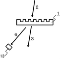
図1に示す本発明の実施形態の分波素子1は透明な平板状基板1aを用いて形成されている。相対する基板表面の一方には、一方向に伸長する凹凸構造が周期的に形成された回折格子1bが備えられて回折格子形成面1cとされていて、他方の基板表面は透過光出射面1dとされている。また、透明基板1aの端面のひとつが分波光出射面1eとされている。分波光出射面1eは、出射角の変動や散乱によるロスを防ぐために、研磨を施す等により平滑とすることが好ましい。さらに、入射光の波長の光に対する低反射コーティングを形成すると、分波光の出射光量を増すことができて好ましい
回折格子形成面1cに入射された入射光2のうち、回折格子1bにより回折されずに直進透過された光は透過光出射面1dから透過光3として出射され、回折格子1bにより回折された回折光は、透過光出射面1dおよび回折格子形成面1cにより全反射されて分波光出射面1eに導かれ分波光6として出射される。出射された分波光6に対して、光検出器13を用いて強度などの特性の測定をおこなうことができる。
A
前記平板状基板は、本発明の分波素子を用いる波長に対して実質的に透明な材料で構成されていればよく、石英ガラス、光学ガラスなどのガラス材料、シリコン、および、ポリカーボネート、ポリメチルメタクリレート(PMMA)などの樹脂材料が例示されるが、耐久性などの観点から石英ガラス、および光学ガラスで攻勢されていることが好ましい。 The flat substrate only needs to be made of a material that is substantially transparent to the wavelength at which the branching element of the present invention is used. Glass material such as quartz glass and optical glass, silicon, polycarbonate, polymethyl Although resin materials, such as a methacrylate (PMMA), are illustrated, it is preferable to be attacked by quartz glass and optical glass from viewpoints, such as durability.
前記凹凸構造は、透明基板自体の表面を加工して作製してもよく、また、透明基板の表面に透明材料からなる層を形成し、かかる層を加工して作製してもよい。かかる加工方法としては、切削、プレス、モールド、フォトリソグラフィグラフィおよびエッチングなどが例示される。 The concavo-convex structure may be produced by processing the surface of the transparent substrate itself, or by forming a layer made of a transparent material on the surface of the transparent substrate and processing the layer. Examples of such processing methods include cutting, pressing, molding, photolithography and etching.
前記凹凸構造を透明材料からなる層を形成、加工して作製する場合、透明材料としては、前述の加工のための加工性に優れたものが好ましく、前述の加工をフォトリソグラフィグラフィおよびエッチングによりおこなうときには、窒化ケイ素、酸化ケイ素、酸化チタン、酸化タンタル、酸化ニオブ、酸化亜鉛、およびシリコンのいずれかから選ばれる1種を主たる成分とする材料が好ましい。 When the concavo-convex structure is formed by forming and processing a layer made of a transparent material, the transparent material preferably has excellent workability for the processing described above, and the processing described above is performed by photolithography and etching. In some cases, a material mainly containing one kind selected from silicon nitride, silicon oxide, titanium oxide, tantalum oxide, niobium oxide, zinc oxide, and silicon is preferable.
また、透明材料として高屈折率材料を用いると、回折効率が高い回折格子が得られ、さらに凹凸部の深さを浅くできるため加工が容易になり好ましい。このような高屈折率の透明材料としては、窒化ケイ素、酸化チタン、酸化タンタル、酸化ニオブ、酸化亜鉛、およびシリコンのいずれかから選ばれる1種を主たる成分とする材料が例示される。 In addition, it is preferable to use a high refractive index material as the transparent material, because a diffraction grating with high diffraction efficiency can be obtained, and the depth of the concavo-convex portion can be reduced, which facilitates processing. Examples of such a high refractive index transparent material include a material mainly composed of one selected from silicon nitride, titanium oxide, tantalum oxide, niobium oxide, zinc oxide, and silicon.
本発明の分波素子に入射した光の挙動について、図2を用いて説明する。本発明の分波素子1の回折格子形成面1cに対して波長λの入射光2を、回折格子形成面1cの法線を含み回折格子1bの凹凸構造の伸長方向と直交する面内で入射角α(すなわち、回折格子形成面1cの法線方向となす角度で図2の符号7)で入射させる。回折格子1bの格子周期をPとすると、入射光2は屈折率nの基板内で(1)式:
sinφ+sinα=m・λ/(n・P) ・・・・・(1)
なる関係を満たす内部回折角φ(図2中の符号8)の方向にm次の回折光4を生じる。ここでmは自然数であり、内部回折角φとは、回折格子1bにより回折され透明基板1a内へ出射される光が、回折格子形成面1cの法線方向となす角である。
The behavior of light incident on the branching element of the present invention will be described with reference to FIG.
sin φ + sin α = m · λ / (n · P) (1)
The mth-order diffracted light 4 is generated in the direction of the internal diffraction angle φ (symbol 8 in FIG. 2) that satisfies the following relationship. Here, m is a natural number, and the internal diffraction angle φ is an angle formed by light diffracted by the diffraction grating 1b and emitted into the transparent substrate 1a with the normal direction of the diffraction
この実施態様の分波素子では、回折格子形成面1cと透過光出射面1dとは平行なので、回折格子形成面1cを内部回折角φで回折された回折光4は、透明基板内を進行して内部回折角φと等しい入射角で透過光出射面1dに入射する。透過光出射面1dに入射した回折光4が、透明基板−空気界面で屈折されて出射されるときの出射角すなわち透過光出射面の法線方向に対する角度θは、内部回折角φと(2)式:
sinθ=n・sinφ ・・・・・(2)
の関係にあり、sinθ≧1のとき、回折光4は、透過光出射面1dを透過することができず、全反射される。透過光出射面1dで全反射された回折光4は、内部屈折角φと等しい角度で回折格子形成面1cに入射するが、一部回折され透過する以外は同様に全反射される。このようにして回折光4は、回折格子形成面1cおよび透過光出射面1dのいずれをも透過することができず、全反射されて基板内を進行し、前記分波光出射面1eに到達する。
In the branching element of this embodiment, since the diffraction
sin θ = n · sin φ (2)
When sin θ ≧ 1, the diffracted light 4 cannot be transmitted through the transmitted
基板内部で偶数回反射されて前記分波折光出射面に到達した光は(3)式、奇数回反射されて前記分波光出射面1eに到達した光は、分波光出射面1eの法線に対して(4)式、
sinψ=n・sin(β−φ) ・・・・・(3)
sinψ=n・sin(β+φ) ・・・・・(4)
をそれぞれ満たす角度すなわち出射角ψ(図2の符号11で表される)の方向に出射される。両式中のβは、前記分波光出射面1eと、回折格子1bが形成された前記回折格子形成面とのなす角である。このときsinψ≧1となると分波光6が分波光出射面1eで全反射されるため、分波光出射面1eから分波光6を取り出すためにはsinψ<1となる必要がある。
角度βを90度とすると、透明基板1aを平行基板面と垂直に切断して分波光出射面1eを形成できるので製造が容易で好ましいが、sinψ<1が満足される範囲で斜めに傾けてもよく、その場合、前記入射光2あるいは前記透過光3の方向に対する前記分波光6の取り出し角を調整することができて好ましい。
The light that has been reflected an even number of times inside the substrate and has reached the demultiplexed light exit surface is expressed by equation (3), and the light that has been reflected an odd number of times and has reached the demultiplexed
sinψ = n · sin (β−φ) (3)
sinψ = n · sin (β + φ) (4)
Are emitted in the direction of the angle satisfying the above, that is, the emission angle ψ (represented by
If the angle β is 90 degrees, the transparent substrate 1a can be cut perpendicularly to the parallel substrate surface to form the demultiplexed
前記回折格子の凹凸構造の周期方向が分波光出射面1eと実質的に垂直でないと、分波光出射面1eへの分波光5の入射角が、前記入射角であるβ−φまたはβ+φと、凹凸構造の伸長方向と分波光出射面1eがなす角度とが合成された角度となり、凹凸構造の周期方向が分波光出射面1eと実質的に垂直である場合と比べて入射角が大きくなり、前記分波光出射面1eで全反射させずに出射させるための制約がきつくなる。すなわち凹凸構造の周期方向が分波光出射面1eと実質的に垂直とすると、回折格子1bや前記角βの選択の幅が広がって好ましい。
If the periodic direction of the concavo-convex structure of the diffraction grating is not substantially perpendicular to the demultiplexed
本発明の分波素子においては、下記のa)、b)、c)が満たされるように前述の回折格子の凸部と凹部との幅の比、回折格子1bの繰返し周期、および凹凸部の深さ、図2の符号12で表される回折格子形成面1cと前記回折格子形成面1cとのなす角β、および回折格子1bへの入射角などの各パラメータの値が決められ、この構成により、回折格子形成面1aに備えられた回折格子1bにより回折格子形成面1cに入射された入射光2を直進透過させて透過光出射面1dから透過光3として出射させるとともに、入射光2の一部を回折格子1bにより回折させ、回折された回折光4を透過光出射面1dにより全反射させて分波光出射面1eに導いて分波光6として出射される。必要に応じて、回折格子1bにより回折された回折光4は透過光出射面1dとおよび回折格子形成面1cとにより全反射させて分波光出射面1eに導かれる。
In the branching element of the present invention, the ratio of the width of the convex portion to the concave portion of the diffraction grating, the repetition period of the diffraction grating 1b, and the concave and convex portions so that the following a), b), and c) are satisfied: The values of parameters such as the depth, the angle β formed between the diffraction
a)分波素子1に入射された入射光が回折されて透明基板内に出射されるために、(1)式においてsinφ<1である。
b)透過光出射面1dにより回折光4が全反射されるために、(2)式においてsinθ≧1である。
c)分波光出射面1eにより分波光5が全反射されず出射されるように、(3)式または(4)式においてsinψ<1である。
a) Since incident light incident on the
b) Since the diffracted light 4 is totally reflected by the transmitted
c) sin ψ <1 in the expression (3) or (4) so that the demultiplexed light 5 is emitted without being totally reflected by the demultiplexed
(1)式におけるmは+1または−1とすることが好ましい。すなわち本発明の分波素子1において、前記回折格子1bにより回折された光のうち+2次以上または−2次以下の高次回折光を用いることもできるが、分波光6として+1次または−1次回折光を用いると、より高次の回折光と比べて大きい回折強度が得られるので、入射光2に対して透過光3および分波光6の強度を高くすることができて好ましい。
In the formula (1), m is preferably +1 or -1. That is, in the
例えば、透明基板1aとして石英ガラスからなる透明基板を用い、前記入射光2として1580〜1620nmの波長帯の光を回折格子形成面1cに垂直入射させる場合には、前記回折格子1bの平行かつ周期的に形成された凹凸構造の周期は1122nmから1580nmとされる。すなわち回折光が透明基板内に回折されるように内部屈折角φを90度未満とするために、凹凸構造の周期は1122nm以上とされる。また、回折光が透明基板内で全反射されるように、内部回折角φを石英ガラスの全反射角度44度より大きくするために、1580nm以下とされる。この構成により、垂直入射された入射光を、透過光出射面1dおよび回折格子形成面1aにより全反射させ、分波光出射面1eへと導くことができる。
For example, when a transparent substrate made of quartz glass is used as the transparent substrate 1a and light having a wavelength band of 1580 to 1620 nm is perpendicularly incident on the diffraction
また、本発明の分波素子1は、回折格子形成面1cに備えられた回折格子1bにより回折された回折光4が、透過光出射面1d、あるいは、回折格子形成面1cと透過光出射面1dとにより全反射されて分波光出射面1eに導かれ出射されるように構成されていれば、前述の透明基体として、透明平板状基板を用いる代わりに、回折格子形成面1cと透過光出射面1dとが平行でない基体を用いることも可能である。
Further, in the branching
また、前記回折格子で回折された前記回折光4が、前記透過光出射面1dで1回全反射された後、前記回折格子形成面1cおよび前記透過光出射面1dでさらに反射されることなく、前記分波光出射面1eから出射されるようにすると、分波素子1内でのロスを減らすことができて好ましい。回折光3は、透明基板1a内を回折格子形成面1cから透過光出射面1dまで進む間に、凹凸構造の周期方向に、回折角と基板厚さに応じた距離だけ変位するので、回折角、基板厚さ、および分波素子に対して入射光を入射させる位置と分波光出射面との距離を調整することにより、この構成とすることができる。例えば、格子周期が1500nmの回折格子が形成された厚さ2mmの石英ガラス基板からなる分波素子に、波長1580〜1620nmでビーム径1mmの入射光を垂直入射させると、この波長帯の光に対する1次回折角は47〜48度であって石英ガラスの全反射角度44度より大きいので、垂直入射された入射光に対する1次回折光は、前記透過光出射面により全反射される。さらに入射光を入射させる位置を、分波光出射面となる平行基板面と端面から2.8mmから3.8mmの距離の点とすると、前記回折格子で回折された回折光は、前記透過光出射面で1回全反射された後、前記および透過光出射面でさらに反射されることなく前記分波光出射面から出射される。
The diffracted light 4 diffracted by the diffraction grating is totally reflected once by the transmitted
また、入射光2を、回折格子形成面の法線方向から凹凸構造の周期方向に傾けるとともに、さらに凹凸構造の伸長方向に対しても傾ける構成とすると、入射光2を回折格子形成面に対して垂直入射させる場合と比べて、回折光4が透過光出射面1dに入射するときの入射角が大きくすることができる。これにより透明基板−空気界面で全反射させる条件を緩和することができるので、回折格子の格子周期を大きくすることができて好ましい。
Further, when the
例として波長が1600nmの光を入射する場合を記す。入射光2を回折格子形成面1cに対して垂直に入射させる場合には、透過光出射面1dにより回折光4を全反射させるために回折格子1bの格子周期を1600nm以下としなければならないが、入射光を回折格子形成面1cの法線方向から凹凸構造の伸長方向すなわち図1の紙面と垂直な方向ヘ10度傾けて入射させた場合には1627nm以下とすることができる。すなわち、格子周期を大きくすることができるので、回折格子の作製が容易になり好ましい。入射光2を、回折格子1bの凹凸構造の伸長方向と直交する面内で格子面の法線方向から傾けるとともに、格子の周期方向と直交する面内で格子面の法線方向から傾けて入射させると、回折光が透明基板と空気との界面で全反射される条件をさらに緩和することができ、回折格子の格子周期をさらに大きくすることができるのでさらに好ましい。
As an example, a case where light having a wavelength of 1600 nm is incident will be described. When the
回折格子1bの前記凹凸構造の断面形状は、矩形または台形とすることが好ましく、このいずれであっても本発明における効果を有するが、矩形に近いものが作製が容易なため好ましい。この断面構造における凹部と凸部との幅の比、凹凸構造の繰返し周期、および凹凸部の深さは、種々の組合せを用いることができる。屈折率1.444の石英ガラス基板の表面を加工して凸部と凹部との幅の比が2:1、格子周期が1500nmの断面形状をもつ回折格子形成するときには、凹凸部の深さを1000nmあるいは3400nmとした構成とすると入射光の偏光方向によらず高い回折効率が得られて好ましいが、適用可能な凹凸部の深さおよび格子周期はこの例に限定されない。また、高屈折率透明材料であるTa2O5膜を石英ガラス基板上に形成し、これを加工して凸部と凹部との幅の比が2:1、凹凸構造の繰返し周期が1500nmの断面形状をもつ回折格子を形成するときには、凹凸部の深さを800nmとする構成が例示される。この構成によれば、格子の周期方向と平行な偏光方向および直交する偏光方向のいずれの偏光方向の直線偏光に対しても、浅い凹凸部深さで高い回折効率を得ることができて好ましいが、これに限定されない。 The cross-sectional shape of the concavo-convex structure of the diffraction grating 1b is preferably rectangular or trapezoidal, and any of these has the effect of the present invention, but a shape close to a rectangle is preferable because it is easy to manufacture. Various combinations can be used for the ratio of the width between the concave portion and the convex portion in this cross-sectional structure, the repetition period of the concave-convex structure, and the depth of the concave-convex portion. When the surface of a quartz glass substrate having a refractive index of 1.444 is processed to form a diffraction grating having a cross-sectional shape with a ratio of the width of the convex portion to the concave portion of 2: 1 and a grating period of 1500 nm, the depth of the concave and convex portion is set. A structure of 1000 nm or 3400 nm is preferable because high diffraction efficiency can be obtained regardless of the polarization direction of incident light, but applicable depth of the uneven portion and grating period are not limited to this example. Further, a Ta 2 O 5 film, which is a high refractive index transparent material, is formed on a quartz glass substrate, and this is processed so that the ratio of the width of the convex portion to the concave portion is 2: 1 and the repetition period of the concave and convex structure is 1500 nm. When a diffraction grating having a cross-sectional shape is formed, a configuration in which the depth of the concavo-convex portion is 800 nm is exemplified. According to this configuration, it is preferable that a high diffraction efficiency can be obtained with a shallow concave-convex portion depth for linearly polarized light in any of the polarization direction parallel to and perpendicular to the periodic direction of the grating. However, the present invention is not limited to this.
また、前記凹凸構造の断面形状を矩形断面に代えて、凹凸構造の伸長方向に垂直な面内において左右非対称とすると、+1次回折光または−1次回折光をいずれか一方の回折効率を大きくすることができる。このとき前記分波光出射面側への回折効率を大きくすると、分波光出射面1eから出射される分波光強度を高めることができて好ましい。左右非対称の断面形状は、鋸歯状、あるいは、所望の鋸歯形状を階段状に近似した断面形状とすることが好ましい。鋸歯形状の断面構造をもつ凹凸構造は、グレースケールマスクを用いたフォトリソグラフィ加工により形成することができる。所望の鋸歯形状を階段状に近似した断面形状は、3〜8ステップのフォトリソグラフィ加工を繰り返すことにより形成することができて、鋸歯形状の断面形状より製造が容易なため好ましい。
Further, when the cross-sectional shape of the concavo-convex structure is changed to a rectangular cross section and is asymmetric in the plane perpendicular to the extending direction of the concavo-convex structure, the diffraction efficiency of either the + 1st order diffracted light or the −1st order diffracted light is increased. Can do. At this time, it is preferable to increase the diffraction efficiency toward the demultiplexed light exit surface, since the intensity of the demultiplexed light emitted from the demultiplexed
また、前記分波光出射面1eとは反対側の端面に入射光の波長の光を反射するミラーを形成すると、分波光出射面1eへの出射光量を増すことができて好ましい。
In addition, it is preferable to form a mirror that reflects light having the wavelength of the incident light on the end surface opposite to the demultiplexed
以下本発明の実施例である例1、2について図面を用いて説明するが、本発明はこれに限定されない。 Hereinafter, Examples 1 and 2 which are embodiments of the present invention will be described with reference to the drawings, but the present invention is not limited thereto.
[例1]
例1の分波素子1は石英ガラス製平板状基板からなる透明基板1aを用いて形成されていて、図3に概略断面図で示した構成をもつ。まず直径125mmで厚さ2.0mm、屈折率1.444の石英ガラスからなる透明基板1aの一方の表面に、フォトリソグラフィグラフィおよびエッチングにより、矩形断面の直線状の溝を周期的に形成して回折格子1bを形成する。前記矩形断面の溝は幅が500nmで深さが3400nmであり、互いに平行に1500nmのピッチで、凸部と凹部との幅の比が2:1とする。回折格子1bを形成した面を回折格子形成面1cとし、この面と対向する表面を透過光出射面1dとする。
次に、ダイシングソーにより、端面が表面に対して直角となるように、前記透明基板を10mm×6mmの長方形に切断する。このとき、回折素子10の短辺を前記回折格子の周期方向と直交するようにし、短辺の端面を平滑に研磨し、前記光の波長に対する低反射コーティングを施し、分波光出射面1eとする。以上の工程により本例の分波素子1を得る。
[Example 1]
The branching
Next, the transparent substrate is cut into a 10 mm × 6 mm rectangle by a dicing saw so that the end face is perpendicular to the surface. At this time, the short side of the diffraction element 10 is orthogonal to the periodic direction of the diffraction grating, the end surface of the short side is polished smoothly, and a low reflection coating for the wavelength of the light is applied to obtain a demultiplexed
このようにして得られた本例の分波素子10の回折格子形成面1cの中央に、波長1580nm、1600nmおよび1620nmの3波長の光が合波された直線偏光の入射光2を垂直入射させる。ここで、前記直線偏光の偏光方向は、回折格子1bの周期方向と平行または直交する方向とする。前記入射光は、前記回折格子を直進透過して透過光出射面から透過光として出射されるとともに、一部は前記回折格子により波長1580nm、1600nmおよび1620nmの波長に応じてそれぞれ内部回折角47度、48度および48度で回折される。それぞれの波長の回折光4は、対向する透過光出射面1dに対してそれぞれの波長の内部回折角と同角度の入射角で入射するが、これらの入射角はいずれも石英ガラスの全反射角度44度より大きいため、全反射される。透過光出射面1dにより全反射された光は、次いで内部回折角と同角度の入射角で回折格子形成面に入射し、同様に全反射される。このように分波された回折光は透過光出射面および回折格子形成面により順次全反射されて、分波光出射面1eから分波光として出射される。
The linearly polarized incident light 2 obtained by combining the light of the three wavelengths of 1580 nm, 1600 nm, and 1620 nm is vertically incident on the center of the diffraction
入射光束の偏光方向を、回折格子の周期方向に対して平行および直交としたときの、それぞれの波長に対する、透明基板の左右の側面から出射される分波光の強度と出射角度、および透過光の強度の測定結果を、表1および2にまとめた。ここで分波光の強度とは、分波光の入射光に対する強度比、分波光の出射角度とは、分波光の出射方向が入射光の入射方向となす角度をいう。 When the polarization direction of the incident light beam is parallel and orthogonal to the periodic direction of the diffraction grating, the intensity and emission angle of the demultiplexed light emitted from the left and right side surfaces of the transparent substrate and the transmitted light for each wavelength. The strength measurement results are summarized in Tables 1 and 2. Here, the intensity of the demultiplexed light refers to the intensity ratio of the demultiplexed light to the incident light, and the emission angle of the demultiplexed light refers to an angle formed by the emission direction of the demultiplexed light and the incident direction of the incident light.

表1および2からわかるように、本例の分波素子1を用いて、入射光を透過させるとともにその一部を分波し、平板状基板の端面のひとつである分波光出射面1eから取り出すことができる。また分波された光は、波長毎に分離して取り出すことができる。
As can be seen from Tables 1 and 2, by using the
[例2]
本例の分波素子は図4に概略断面図を示すように、厚さ2.0mmの石英ガラス製平板状基板からなる透明基板1aを用い、その一方の面にスパッタリング法により成膜された屈折率が2.107で厚さ800nmのTa2O5膜を、フォトリソグラフィおよびドライエッチングにより格子状の溝が周期的に配列された回折格子1bに加工して、形成される。すなわち、本例の回折格子1bは、屈折率が2.107で幅1000nm、高さ800nmの凸部が、1500nmの周期で配列された構造をもつ。
次に、ダイシングソーにより、端面が平行基板面に対して直角となるように、前記透明基板を6mm×6mmの正方形に切り出す。このとき、回折素子1の一辺を、前記回折格子の長手方向と平行となるようにし、この辺の端面を平滑に研磨し、前記光の波長に対する低反射コーティングを施し、分波光出射面1eとする。以上の工程により本例の分波素子1を得る。
[Example 2]
As shown in the schematic cross-sectional view of FIG. 4, the branching element of this example was formed by sputtering on one surface of a transparent substrate 1a made of a quartz glass flat substrate having a thickness of 2.0 mm. A Ta 2 O 5 film having a refractive index of 2.107 and a thickness of 800 nm is formed into a diffraction grating 1b in which grating-like grooves are periodically arranged by photolithography and dry etching. That is, the diffraction grating 1b of this example has a structure in which convex portions having a refractive index of 2.107, a width of 1000 nm, and a height of 800 nm are arranged with a period of 1500 nm.
Next, the transparent substrate is cut into a 6 mm × 6 mm square by a dicing saw so that the end surface is perpendicular to the parallel substrate surface. At this time, one side of the
前記3つの波長の光が合波された直線偏光の入射光2を垂直入射させると、例1と同様に、入射光2は透過光3として直進透過されるとともに、一部は前記回折格子により波長1580nm、1600nmおよび1620nmの波長に応じてそれぞれ内部回折角47度、48度および48度で回折される。回折光は対向する透過光出射面に対して同角度で入射するが、いずれも石英ガラスの全反射角度44度より大きいため全反射され、分波光出射面1eから分波光として出射される。
When linearly polarized incident light 2 obtained by combining the three wavelengths of light is vertically incident, the
入射光束の偏光方向を、回折格子の周期方向に対して平行および直交としたときの、分波光の強度と出射角度、および透過光の強度の測定結果を、表3および4にまとめた。ここで分波光の強度とは、分波光の入射光に対する強度比、分波光の出射角度とは、分波光の出射方向が入射光の入射方向となす角度をいう。 Tables 3 and 4 summarize the measurement results of the intensity and emission angle of the demultiplexed light and the intensity of the transmitted light when the polarization direction of the incident light beam is parallel and orthogonal to the periodic direction of the diffraction grating. Here, the intensity of the demultiplexed light refers to the intensity ratio of the demultiplexed light to the incident light, and the emission angle of the demultiplexed light refers to an angle formed by the emission direction of the demultiplexed light and the incident direction of the incident light.
表3および4からわかるように、本例の分波素子1を用いて、入射光を透過させるとともにその一部を分波し、平板状基板の端面のひとつである分波光出射面1eから取り出すことができる。また分波された光は、波長毎に分離して取り出すことができる。
As can be seen from Tables 3 and 4, by using the
本発明の分波素子は小型で、入射光の入射位置、透過光の出射位置から離れた位置から分波光を出射させることができるので、分波光の強度や波長などの特性を測定する光検出器やその配置に対する制約が小さい。このため、入射光の特性を透過させつつモニターする測定系をコンパクトな構成で実現できる。 Since the demultiplexing element of the present invention is small and can emit demultiplexed light from a position away from the incident position of incident light and the output position of transmitted light, light detection that measures characteristics such as intensity and wavelength of demultiplexed light There are few restrictions on the container and its arrangement. Therefore, it is possible to realize a measurement system that monitors while transmitting the characteristics of incident light with a compact configuration.
1:分波素子
1a:透明平板状基板
1b:回折格子
1c:回折格子形成面
1d:透過光出射面
1e:分波光出射面
2:入射光
3:透過光
4:回折光
5:透過光出射面により全反射された回折光
6:光検出器
7:入射光の回折格子形成面への入射角
8:内部回折角
9:回折光の透過光出射面への入射角
10:回折光の分波光出射面への入射角
11:分波光の分波光出射面からの出射角
12:入射光の方向に対する分波光の取出し角
13:光検出器
23:低反射コーティング
1: Demultiplexing element 1a: Transparent flat substrate 1b: Diffraction grating 1c: Diffraction grating forming
Claims (11)
前記回折格子形成面は、一方向に伸長する凹凸構造が周期的に形成された回折格子を備えていて、
前記分波素子は、前記回折格子形成面に入射した入射光を直進透過させて透過光出射面から出射させるとともに前記入射光の一部を回折させ、前記回折された回折光を前記透明基体内で前記透過光出射面により全反射させて前記分波光出射面へ導き、前記分波光出射面より分波光として出射させることを特徴とする分波素子。 A demultiplexing device comprising a transparent substrate having a diffraction grating forming surface, a transmitted light emitting surface, and a demultiplexed light emitting surface,
The diffraction grating forming surface includes a diffraction grating in which a concavo-convex structure extending in one direction is periodically formed,
The demultiplexing element causes the incident light incident on the diffraction grating forming surface to pass straight through and be emitted from the transmitted light exit surface, diffracts a part of the incident light, and causes the diffracted diffracted light to pass through the transparent substrate. The demultiplexing element according to claim 1, wherein the demultiplexing element is totally reflected by the transmitted light exit surface, guided to the demultiplexed light exit surface, and emitted as demultiplexed light from the demultiplexed light exit surface.
前記分波素子が、
透明材料からなる平板状基板を用いて形成されていて、
前記平板状基板の相対する基板表面の、一方の表面が一方向に伸長する凹凸構造が周期的に形成された回折格子が備えられた回折格子形成面とされ、他方の表面が透過光出射面とされていて、端面の1つが平坦で前記回折格子の凹凸構造の周期方向と実質的に垂直に配設され前記分波光出射面とされている分波素子であって、
前記分波素子の前記回折格子形成面に入射させた前記入射光を、前記透明基体の全反射角より大きい回折角で回折させて前記透明基体内を前記分波光出射面へ導き、前記分波光出射面から分波光として出射させることを特徴とする分波方法。
In a demultiplexing method in which incident light is incident on a demultiplexing element to be transmitted in a straight line and a part of the incident light is changed as a demultiplexed light by changing the optical path.
The branching element is
It is formed using a flat substrate made of a transparent material,
One of the opposing substrate surfaces of the flat substrate is a diffraction grating forming surface provided with a diffraction grating in which an uneven structure with one surface extending in one direction is periodically formed, and the other surface is a transmitted light emitting surface. A demultiplexing element in which one of the end faces is flat and is disposed substantially perpendicular to the periodic direction of the concavo-convex structure of the diffraction grating and serves as the demultiplexed light exit surface,
The incident light incident on the diffraction grating forming surface of the demultiplexing element is diffracted at a diffraction angle larger than the total reflection angle of the transparent substrate to guide the inside of the transparent substrate to the demultiplexed light exit surface, and the demultiplexed light A demultiplexing method characterized by emitting light as demultiplexed light from an emission surface.
Priority Applications (1)
| Application Number | Priority Date | Filing Date | Title |
|---|---|---|---|
| JP2005078702A JP2006259439A (en) | 2005-03-18 | 2005-03-18 | Demultiplexing element and demultiplexing method |
Applications Claiming Priority (1)
| Application Number | Priority Date | Filing Date | Title |
|---|---|---|---|
| JP2005078702A JP2006259439A (en) | 2005-03-18 | 2005-03-18 | Demultiplexing element and demultiplexing method |
Publications (2)
| Publication Number | Publication Date |
|---|---|
| JP2006259439A true JP2006259439A (en) | 2006-09-28 |
| JP2006259439A5 JP2006259439A5 (en) | 2008-02-21 |
Family
ID=37098761
Family Applications (1)
| Application Number | Title | Priority Date | Filing Date |
|---|---|---|---|
| JP2005078702A Withdrawn JP2006259439A (en) | 2005-03-18 | 2005-03-18 | Demultiplexing element and demultiplexing method |
Country Status (1)
| Country | Link |
|---|---|
| JP (1) | JP2006259439A (en) |
Cited By (2)
| Publication number | Priority date | Publication date | Assignee | Title |
|---|---|---|---|---|
| JP2018179866A (en) * | 2017-04-19 | 2018-11-15 | 株式会社ミツトヨ | Optical encoder |
| DE102018124314A1 (en) * | 2018-10-02 | 2020-04-02 | Carl Zeiss Smt Gmbh | Device for determining the exposure energy when exposing an element in an optical system, in particular for microlithography |
-
2005
- 2005-03-18 JP JP2005078702A patent/JP2006259439A/en not_active Withdrawn
Cited By (5)
| Publication number | Priority date | Publication date | Assignee | Title |
|---|---|---|---|---|
| JP2018179866A (en) * | 2017-04-19 | 2018-11-15 | 株式会社ミツトヨ | Optical encoder |
| DE102018124314A1 (en) * | 2018-10-02 | 2020-04-02 | Carl Zeiss Smt Gmbh | Device for determining the exposure energy when exposing an element in an optical system, in particular for microlithography |
| DE102018124314B4 (en) * | 2018-10-02 | 2020-10-22 | Carl Zeiss Smt Gmbh | Device for determining the exposure energy when exposing an element in an optical system, in particular for microlithography |
| DE102018124314B9 (en) * | 2018-10-02 | 2020-12-31 | Carl Zeiss Smt Gmbh | Device for determining the exposure energy when exposing an element in an optical system, in particular for microlithography |
| US11079604B2 (en) | 2018-10-02 | 2021-08-03 | Carl Zeiss Smt Gmbh | Device for determining the exposure energy during the exposure of an element in an optical system, in particular for microlithography |
Similar Documents
| Publication | Publication Date | Title |
|---|---|---|
| US7170600B2 (en) | Spectrometer using diffraction grating | |
| JP4475501B2 (en) | Spectroscopic element, diffraction grating, composite diffraction grating, color display device, and duplexer | |
| US9176282B2 (en) | High efficiency mono-order concave diffraction grating | |
| US7349612B2 (en) | Optical element, optical circuit provided with the optical element, and method for producing the optical element | |
| US7075722B2 (en) | Diffractive optical element and optical system having the same | |
| US7386205B2 (en) | Optical device and method for making same | |
| JP5050594B2 (en) | Spectrometer | |
| KR101226346B1 (en) | Optical element, optical apparatus, optical pickup, optical information processing apparatus, optical attenuator, polarization conversion element, projector optical system, and optical apparatus system | |
| EP2803123B1 (en) | Integrated sub-wavelength grating system | |
| US9726794B2 (en) | High index contrast grating structure for light manipulation and related method | |
| JP2010210824A (en) | Optical element and illumination device | |
| US4838645A (en) | Reflecting diffraction grating | |
| KR20140082855A (en) | Control of light wavefronts | |
| JP2003255113A (en) | Light separation element and optical appliance using the same | |
| US20020122613A1 (en) | Optical device and spectroscopic and integrated optical apparatus using the same | |
| US6914715B2 (en) | Optical element | |
| JP2006259439A (en) | Demultiplexing element and demultiplexing method | |
| JP2004205880A (en) | Reflective diffraction grating | |
| JP2007058102A (en) | Optical multiplexer/demultiplexer and optical multiplexing unit | |
| JP2003066269A (en) | Multi-wavelength demultiplexing optical device and wavelength multiplexed light transmission module | |
| JP2012058218A5 (en) | ||
| JP6976516B2 (en) | How to use and design transmission gratings, optical waveguides, and transmission gratings | |
| US6718092B2 (en) | Frequency detection, tuning and stabilization system | |
| CN1246716C (en) | Low return loss etching diffraction grating wave-length division multiplexer | |
| JP5834567B2 (en) | Detection device and method for manufacturing spectroscopic device |
Legal Events
| Date | Code | Title | Description |
|---|---|---|---|
| A521 | Written amendment |
Free format text: JAPANESE INTERMEDIATE CODE: A523 Effective date: 20080107 |
|
| A621 | Written request for application examination |
Free format text: JAPANESE INTERMEDIATE CODE: A621 Effective date: 20080107 |
|
| A977 | Report on retrieval |
Free format text: JAPANESE INTERMEDIATE CODE: A971007 Effective date: 20100204 |
|
| A131 | Notification of reasons for refusal |
Free format text: JAPANESE INTERMEDIATE CODE: A131 Effective date: 20100209 |
|
| A761 | Written withdrawal of application |
Free format text: JAPANESE INTERMEDIATE CODE: A761 Effective date: 20100325 |