JP2006252995A - Charged particle beam apparatus - Google Patents
Charged particle beam apparatus Download PDFInfo
- Publication number
- JP2006252995A JP2006252995A JP2005068781A JP2005068781A JP2006252995A JP 2006252995 A JP2006252995 A JP 2006252995A JP 2005068781 A JP2005068781 A JP 2005068781A JP 2005068781 A JP2005068781 A JP 2005068781A JP 2006252995 A JP2006252995 A JP 2006252995A
- Authority
- JP
- Japan
- Prior art keywords
- sample
- charged particle
- particle beam
- stage
- beam apparatus
- Prior art date
- Legal status (The legal status is an assumption and is not a legal conclusion. Google has not performed a legal analysis and makes no representation as to the accuracy of the status listed.)
- Pending
Links
Images


Classifications
-
- H—ELECTRICITY
- H01—ELECTRIC ELEMENTS
- H01J—ELECTRIC DISCHARGE TUBES OR DISCHARGE LAMPS
- H01J37/00—Discharge tubes with provision for introducing objects or material to be exposed to the discharge, e.g. for the purpose of examination or processing thereof
- H01J37/26—Electron or ion microscopes; Electron or ion diffraction tubes
- H01J37/28—Electron or ion microscopes; Electron or ion diffraction tubes with scanning beams
-
- G—PHYSICS
- G01—MEASURING; TESTING
- G01N—INVESTIGATING OR ANALYSING MATERIALS BY DETERMINING THEIR CHEMICAL OR PHYSICAL PROPERTIES
- G01N23/00—Investigating or analysing materials by the use of wave or particle radiation, e.g. X-rays or neutrons, not covered by groups G01N3/00 – G01N17/00, G01N21/00 or G01N22/00
- G01N23/22—Investigating or analysing materials by the use of wave or particle radiation, e.g. X-rays or neutrons, not covered by groups G01N3/00 – G01N17/00, G01N21/00 or G01N22/00 by measuring secondary emission from the material
- G01N23/225—Investigating or analysing materials by the use of wave or particle radiation, e.g. X-rays or neutrons, not covered by groups G01N3/00 – G01N17/00, G01N21/00 or G01N22/00 by measuring secondary emission from the material using electron or ion
-
- H—ELECTRICITY
- H01—ELECTRIC ELEMENTS
- H01J—ELECTRIC DISCHARGE TUBES OR DISCHARGE LAMPS
- H01J2237/00—Discharge tubes exposing object to beam, e.g. for analysis treatment, etching, imaging
- H01J2237/26—Electron or ion microscopes
- H01J2237/28—Scanning microscopes
- H01J2237/2803—Scanning microscopes characterised by the imaging method
- H01J2237/2807—X-rays
-
- H—ELECTRICITY
- H01—ELECTRIC ELEMENTS
- H01J—ELECTRIC DISCHARGE TUBES OR DISCHARGE LAMPS
- H01J2237/00—Discharge tubes exposing object to beam, e.g. for analysis treatment, etching, imaging
- H01J2237/26—Electron or ion microscopes
- H01J2237/28—Scanning microscopes
- H01J2237/2813—Scanning microscopes characterised by the application
- H01J2237/2817—Pattern inspection
Abstract
Description
本発明は、IC,LSI等の半導体デバイスの製造プロセスにおける試料の検査、特に、試料のエッジ部等の検査を行うのに適した荷電粒子ビーム装置に関する。 The present invention relates to a charged particle beam apparatus suitable for inspecting a sample in a manufacturing process of a semiconductor device such as an IC or LSI, in particular, inspecting an edge portion or the like of a sample.
IC,LSI等の半導体デバイスの製造プロセスにおいては、半導体素子が作製されるウエハの如き基板(以後試料と称す)の観察等を通して試料の検査が行われている。 In a manufacturing process of a semiconductor device such as an IC or LSI, a sample is inspected through observation of a substrate (hereinafter referred to as a sample) such as a wafer on which a semiconductor element is manufactured.
この様な試料の検査は、例えば、走査電子顕微鏡(SEM)の電子ビーム照射により、非破壊で行われている。 Such sample inspection is performed non-destructively by, for example, electron beam irradiation of a scanning electron microscope (SEM).
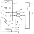
図1は、試料の検査を行う走査電子顕微鏡の概略を示したものである。 FIG. 1 shows an outline of a scanning electron microscope for inspecting a sample.
図中1は電子光学鏡筒で、真空チャンバー2の上部壁に取り付けられている。
In the figure,
鏡筒1内には、電子銃3,該電子銃からの電子ビームを試料上に集束させるための集束レンズ4と対物レンズ5,前記電子銃1からの電子ビームで試料上を走査させるための偏向器6、試料からの二次電子を検出するための軸対称二次電子検出器7等が設けられている。尚、前記偏向器6は、X方向偏向器とY方向偏向器から成る。
In the
前記真空チャンバー2内には、上面に静電チャック8を取り付けたステージ9が設けられており、前記静電チャック8に試料10がホールドされる様に成っている。尚、ステージ9は、中心軸Oに垂直な面上に試料10を移動させることが出来るように、X方向移動用とY方向移動用のステージから成っている。
In the vacuum chamber 2, a
さて、制御装置11からの指令により作動する走査制御回路12から走査信号が偏向器5に送られると、試料10上に集束された電子ビームは、試料表面上の所定の領域を二次元的に走査する。この走査により、試料10から発生した二次電子は二次電子検出器7に検出される。二次電子検出器7の出力は増幅器13により増幅され、前記制御装置11に送られる。該制御装置は、入力されて来た二次電子信号を画像信号処理を施して表示装置14に送り、試料の二次電子像を表示させる。
Now, when a scanning signal is sent to the
尚、図1では図示しなかったが、試料上方には、X線検出器も設けられており、試料の所定領域に電子ビームが照射された時に、該領域から発生した特性X線を該X線検出器で検出し、その特性X線信号を前記制御装置11に送るようにしている。該制御装置は、送られて来た特性X線信号に基づいて、前記所定領域部分の元素分析を行う。 Although not shown in FIG. 1, an X-ray detector is also provided above the sample, and when an electron beam is irradiated onto a predetermined region of the sample, characteristic X-rays generated from the region are displayed on the X-ray. It is detected by a line detector and its characteristic X-ray signal is sent to the control device 11. The control device performs elemental analysis of the predetermined region portion based on the characteristic X-ray signal sent thereto.
オペレータは前記所定領域の二次電子像の観察や前記元素分析に基づいて、試料の検査を行っている。 The operator inspects the sample based on the observation of the secondary electron image of the predetermined region and the elemental analysis.
さて、前記の如き試料検査は、主に、試料の表面について行われている。 The sample inspection as described above is mainly performed on the surface of the sample.
しかし、近年、試料の表面だけではなく、試料の側面及びその近傍(エッジ部)や裏面についての検査の必要性が高まっている。その理由は、以下の通りである。 However, in recent years, not only the surface of the sample but also the side surface of the sample and its vicinity (edge portion) and the back surface need to be inspected. The reason is as follows.
半導体基板の代表であるシリコンウエハは、コストダウンなどを考慮して、直径50mm,75mm,100mm,125mm,150mm,200mmと漸次大きなものが出現し、最近では300mmのものが出現している。しかし、直径が大きくなっているが厚さはさほど変わっておらず、その為に、ウエハのエッジ部に傷や欠け等があると、ウエハ自体が割れ易くなる。 Silicon wafers, which are representative of semiconductor substrates, are gradually increasing in diameters of 50 mm, 75 mm, 100 mm, 125 mm, 150 mm, and 200 mm in consideration of cost reduction, and recently, 300 mm wafers have appeared. However, although the diameter is increased, the thickness is not changed so much. Therefore, if the edge portion of the wafer has scratches or chips, the wafer itself is easily broken.
又、ウエハのエッジ部にパーティクルが付いている場合があり、その様な場合、パーティクルは工程が進に連れてパターンが形成されている鏡面部に転移して付着したり、或いは、熱処理によって取れて鏡面部に膜状に付着したりする。 In some cases, particles may be attached to the edge portion of the wafer. In such a case, the particles are transferred to the mirror surface portion where the pattern is formed as the process proceeds, or are removed by heat treatment. Or adhere to the mirror surface in the form of a film.
又、ウエハの裏面にパーティクルが付着していると、ウエハ支持部材にパーティクルが付き、次に支持されるウエハの表面を汚すことがある。 Further, if particles adhere to the back surface of the wafer, the particles may adhere to the wafer support member, and the surface of the next supported wafer may be soiled.
何れの場合においても、ウエハ自体が不良品になる恐れがある。 In either case, the wafer itself may become a defective product.
従って、シリコンウエハのエッジ部や裏面に、傷,欠け,及びパーティクル等が無いかどうか検査する必要がある。 Therefore, it is necessary to inspect whether there are any scratches, chips, particles, or the like on the edge or back surface of the silicon wafer.
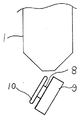
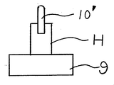
先ず、エッジ部の検査については、例えば、図2に示す様に、ステージ9を傾斜させることにより試料10を傾斜させ(試料を傾斜させる機構は、例えば、特開平09−17370号公報に示されている)、エッジ部が鏡筒1に対向するようにすれば可能である。或いは、試料を傾斜させずに、鏡筒自体を傾斜させても良い。或いは、図3に示す様に、試料を割ってエッジ部を含む部分10´を、そのエッジ部が鏡筒1に対向するようにホルダーHに支持させることにより可能である。
First, as for the inspection of the edge portion, for example, as shown in FIG. 2, the
一方、裏面の検査については、試料の裏面が鏡筒に対向するように静電チャックに支持させることにより可能である。 On the other hand, the back surface can be inspected by supporting the sample on the electrostatic chuck so that the back surface of the sample faces the lens barrel.
しかし、試料や鏡筒を傾斜する方式では、試料の裏面に近いエッジ部分や裏面を検査することは難しい。 However, it is difficult to inspect the edge portion and the back surface close to the back surface of the sample in the method in which the sample and the lens barrel are inclined.
又、試料を割る方式では、試料を破壊することになるので、インラインでの検査は出来ない。 In addition, in the method of breaking the sample, the sample is destroyed, so in-line inspection is not possible.
又、試料を裏返しにしてホルダーに支持させる方式は、パターンが形成されている試料表面を傷めるために、インラインでの検査は出来ない。 Further, the method of turning the sample upside down and supporting it on the holder damages the surface of the sample on which the pattern is formed, so that in-line inspection cannot be performed.
本発明はこの様な問題点を解決するために成されたもので、新規な荷電粒子ビーム装置を提供することを目的とする。 The present invention has been made to solve such problems, and an object thereof is to provide a novel charged particle beam apparatus.
本発明の荷電粒子ビーム装置は、荷電粒子ビーム発生手段,該発生手段からのビームを試料上に集束させるための集束手段,及び前記発生手段からのビームで試料上を走査させるための偏向手段を備えた荷電粒子ビーム鏡筒が、内部に試料を載置するステージが設けられているチャンバーに少なくとも2本設けられた装置であって、荷電粒子ビームの照射により試料から発生した粒子の検出手段と、検出手段からの信号に基づいて少なくとも試料の一部分に関する像を表示する手段とを備えた荷電粒子ビーム装置において、一方の鏡筒は、該鏡筒からの荷電粒子ビームが、少なくとも試料側面の上側を走査出来る位置に、他方の鏡筒は、荷電粒子ビームが、少なくとも試料側面の下側を走査出来る位置に、それぞれ設けられていることを特徴とする。 The charged particle beam apparatus of the present invention comprises charged particle beam generating means, focusing means for focusing the beam from the generating means on the sample, and deflecting means for scanning the sample with the beam from the generating means. The charged particle beam column provided is a device provided with at least two chambers in which a stage for placing a sample is provided, and means for detecting particles generated from the sample by irradiation with the charged particle beam; And a means for displaying an image relating to at least a part of the sample based on a signal from the detection means, wherein one of the lens barrels is such that the charged particle beam from the lens barrel is at least above the side surface of the sample. The other lens barrel is provided at a position where the charged particle beam can scan at least the lower side of the side surface of the sample. To.
本発明の荷電粒子ビーム装置は、荷電粒子ビーム発生手段,該発生手段からのビームを試料上に集束させるための集束手段,及び前記発生手段からのビームで試料上を走査させるための偏向手段を備えた荷電粒子ビーム鏡筒が、内部に試料を載置するステージが設けられているチャンバーに少なくとも2本設けられた装置であって、荷電粒子ビームの照射により試料から発生した粒子の検出手段と、検出手段からの信号に基づいて少なくとも試料の一部分に関する像を表示する手段とを備えた荷電粒子ビーム装置において、一方の鏡筒は、試料の表面と裏面の中間面の延長面より上方の位置に、他方の鏡筒は、前記延長面より下方の位置に、それぞれ設けられていることを特徴とする。 The charged particle beam apparatus of the present invention comprises charged particle beam generating means, focusing means for focusing the beam from the generating means on the sample, and deflecting means for scanning the sample with the beam from the generating means. The charged particle beam column provided is a device provided with at least two chambers in which a stage for placing a sample is provided, and means for detecting particles generated from the sample by irradiation of a charged particle beam; And a means for displaying an image relating to at least a part of the sample based on a signal from the detection means, wherein one of the lens barrels is positioned above the extended surface of the intermediate surface between the front surface and the back surface of the sample. In addition, the other lens barrel is provided at a position below the extension surface.
本発明では、荷電粒子ビーム発生手段,該発生手段からのビームを試料上に集束させるための集束手段,及び前記発生手段からのビームで試料上を走査させるための偏向手段を備えた荷電粒子ビーム鏡筒が、内部に試料を載置するステージが設けられるチャンバーに少なくとも2本設けられた装置で、一方の鏡筒は、該鏡筒からの荷電粒子ビームが、少なくとも試料側面の上側を走査出来る位置に、他方の鏡筒は、荷電粒子ビームが、少なくとも試料側面の下側を走査出来る位置にそれぞれ設けているので、容易に、試料の裏面に近いエッジ部分や裏面の一部を検査することが可能である。又、試料や試料上に形成されたパターン等を破壊することが無いので、インラインでの検査は可能である。 In the present invention, a charged particle beam comprising a charged particle beam generating means, a focusing means for focusing the beam from the generating means on the sample, and a deflecting means for scanning the sample with the beam from the generating means. The lens barrel is an apparatus provided with at least two chambers in which a stage on which a sample is placed is provided. One of the lens barrels can scan at least the upper side of the sample side surface with a charged particle beam from the lens barrel. Since the other lens barrel is provided at a position where the charged particle beam can scan at least the lower side of the sample side surface, the edge part close to the back surface of the sample and a part of the back surface can be easily inspected. Is possible. In addition, since the sample and the pattern formed on the sample are not destroyed, in-line inspection is possible.
以下、図面を参照して本発明の実施の形態を詳細に説明する。 Hereinafter, embodiments of the present invention will be described in detail with reference to the drawings.
図4は本発明の荷電粒子ビーム装置の一例として示した電子ビーム検査装置の一概略例を示したものである。図中、図1にて使用した記号と同一記号の付されたものは同一構成要素を示す。 FIG. 4 shows a schematic example of an electron beam inspection apparatus shown as an example of the charged particle beam apparatus of the present invention. In the figure, the same reference numerals as those used in FIG. 1 denote the same components.
図中15は真空チャンバーで、その内部、ほぼ中央部に、上面に静電チャック8を取り付けたステージ9が設けられている。該ステージは、試料10を中心軸Oに垂直な面に沿って回転させることが出来る回転ステージ9A,X方向移動用ステージ9B,Y方向移動用ステージ9Cから成っている。前記静電チャック8には試料10がホールドされる様に成っている。
In the figure,
1A,1Bは、前記図1に示す電子光学鏡筒1と同様な構成の第1,第2電子光学鏡筒で、鏡筒内には、電子銃3A,3B、集束レンズ4A,4B、対物レンズ5A,5B、偏向器6A,6B、軸対称二次電子検出器7A,7B等が設けられている。
Reference numerals 1A and 1B denote first and second electron optical barrels having the same configuration as the electron
前記第1電子光学鏡筒1Aは、試料10が初期の位置(基準位置)にある時に、少なくとも試料側面の上側半分を走査出来き、試料をX,Y方向の二次元方向に移動させ、試料10を図の右側に移動させた時に、少なくとも試料10の上面を走査出来る様に、試料10の表面と裏面の中間面の延長面より上方の真空チャンバー15の側壁に取り付けられている。
The first electron optical column 1A can scan at least the upper half of the side surface of the sample when the
一方、前記第2電子光学鏡筒1Bは、試料10が初期の位置(基準位置)にある時に、少なくとも試料側面の下側半分を走査出来き、試料をX,Y方向の二次元方向に移動させ、試料10を図の右側に移動させた時に、少なくとも試料10の下面を走査出来る様に、試料10の表面と裏面の中間面の延長面より下方の真空チャンバー15の側壁に取り付けられている。
On the other hand, the second electron optical column 1B can scan at least the lower half of the side surface of the sample when the
尚、12A,12Bは制御装置11からの指令に基づきそれぞれ偏向器6A,6Bに走査信号を供給する走査制御回路、13A,13Bは前記各軸対称二次電子検出器7A,7Bからの検出信号を増幅するための増幅器である。
さて、試料10を基準位置にしておき、制御装置11からの指令により走査制御回路12A,12Bから走査信号をそれぞれ偏向器6A,6Bに走査信号を送る。
Now, the
電子銃3Aから発生された電子ビームは試料10の側面上部に集束され、該側面の上側面表面上を二次元的に走査する。この走査により、試料10から発生した二次電子は二次電子検出器7Aに検出される。二次電子検出器7Aの出力は増幅器13Aにより増幅され、前記制御装置11に送られる。該制御装置は、入力されて来た二次電子信号を画像信号処理を施して表示装置14に送る。
The electron beam generated from the
一方、電子銃3Bから発生された電子ビームは試料10の側面下部に集束され、該側面の下側面表面上を二次元的に走査する。この走査により、試料10から発生した二次電子は二次電子検出器7Bに検出される。二次電子検出器7Bの出力は増幅器13Bにより増幅され、前記制御装置11に送られる。該制御装置は、入力されて来た二次電子信号を画像信号処理を施して表示装置14に送る。
On the other hand, the electron beam generated from the
この際、前記制御装置11は、図5に示す様に、例えば、表示装置14の表示画面の上半分の部分Uに二次電子検出器7Aの出力信号に基づいて、試料側部の上半分の二次電子像を、表示画面の下半分の部分Dに二次電子検出器7Bの出力信号に基づいて試料側部の下半分の二次電子像を表示させる。
At this time, as shown in FIG. 5, for example, the control device 11 is arranged on the upper half portion U of the display screen of the
次に、制御装置11からの指令により回転ステージ9Aを間歇的に回転させ、停止の度に、前記側面上部と下部を各鏡筒の電子ビームで走査することにより、側面全周における側面上部と下部の像が得られる。尚、図4では図示しなかったが、各鏡筒の近傍には、それぞれ、X線検出器も設けられており、電子ビーム照射により、試料側面上部,下部各々から発生した特性X線を各X線検出器で検出し、その特性X線信号を前記制御装置11に送るようにしている。該制御装置は、送られて来た特性X線信号に基づいて、各部の元素分析を行っている。
Next, the
尚、前記例では、各二次電子検出器7A,7Bを各鏡筒1A,1B内に設けたが、図6の7A´,7B´に示す様に、各鏡筒の真横(例えば、左側)に置いても良い。この様に成せば、試料10から低角度で放出される二次電子を検出することが出来るので、陰影感のある二次電子像が得られる。この時、鏡筒を挟んで二次電子検出器7A´,7B´の配置位置と反対側の位置(鏡筒の右側)に、それぞれ、X線検出器8A´,8B´(図示されていない)を配置しても良い。
In the above example, the
この様にすれば、試料の側面における上部と下部の二次電子像が図4に示す例と同様に得られると同時に、各部のX線分析も行える。 In this way, the upper and lower secondary electron images on the side surface of the sample can be obtained in the same manner as in the example shown in FIG. 4, and X-ray analysis of each part can be performed.
又、前記各例の様に、二次電子検出器とX線検出器を各鏡筒毎に設けず、図7に示す様に、2つの鏡筒1A,1Bの中間位置の左右に互いに離して二次電子検出器20,X線検出器30を配置させるようにしても良い。尚、図7(a),(b)は、それぞれ、中心軸Oに垂直な方向から見た図、中心軸O方向に沿って上方から見た図である。この様な構成にして、順番に、電子光学鏡筒の電子銃や光学系を作動させ、電子銃からの電子ビームで、試料10の側面の上部分、下部分を順次走査することにより、試料側部の上半分、下半部の二次電子像が得られる。尚、この場合も、試料10から低角度で放出される二次電子を検出することが出来るので、陰影感のある二次電子像が得られる。
Further, as in each of the above examples, a secondary electron detector and an X-ray detector are not provided for each lens barrel, and as shown in FIG. 7, they are separated from each other at the left and right of the intermediate position between the two lens barrels 1A and 1B. The
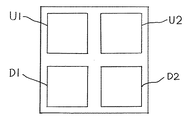
又、図4に示した様に各鏡筒内と、図6に示した様に各鏡筒外に、それぞれ、二次電子検出器を設け、2つの電子光学鏡筒1A,1Bからの電子ビームで、同時にそれぞれ、試料10の側面の上部,下部を走査し、それぞれの検出器で検出された二次電子信号を制御装置11に送り、第1電子光学鏡筒内の二次電子検出器、第2電子光学鏡筒内の二次電子検出器、第1電子光学鏡筒外の二次電子検出器、第2電子光学鏡筒外の二次電子検出器各々で検出した二次電子に基づく像を、表示装置14の表示画面のU1,D1,U2,D2の部分(図8)にそれぞれ表示されるようにしても良い。この様に成せば、表示部分U2,D2にそれぞれ表示された試料10の側面の上部,下部の二次電子像は陰影感のある像となる。
In addition, secondary electron detectors are provided in each barrel as shown in FIG. 4 and outside each barrel as shown in FIG. 6, respectively, and electrons from the two electron optical barrels 1A and 1B are provided. The beam simultaneously scans the upper and lower sides of the side surface of the
又、試料10の裏面や上面を検査する場合には、制御装置11からの指令に基づき、X方向移動用ステージ9B,Y方向移動用ステージ9Cにより試料10を初期の位置(基準位置)から適宜鏡筒方向に移動させ、前記第1電子光学鏡筒1Aの電子銃3Aからの電子ビームが試料上面を走査出来るように、前記第2電子光学鏡筒1Bの電子銃3Bからの電子ビームが試料裏面を走査出来るようにする。
When inspecting the back and top surfaces of the
尚、前記各例では、二次電子像を表示するように成したが、試料からの反射電子を検出して、反射電子像を表示させるようにしても良い。 In each of the above examples, the secondary electron image is displayed. However, the reflected electron image from the sample may be detected to display the reflected electron image.
又、特開平09−017370号公報に示す様な傾斜機構を使用し、試料10を中心軸Oに垂直な面に対して傾け、その状態で、第2電子ビーム光学鏡筒2Bからの電子ビームで試料裏面を走査して、試料裏面からの二次電子信号等により試料裏面を検査したり、第1電子ビーム光学鏡筒2Aからの電子ビームで試料表面を走査して、試料上面からの二次電子信号等により試料上面を検査したりするように成しても良い。
Further, the tilting mechanism as shown in Japanese Patent Laid-Open No. 09-018370 is used, the
又、前記例では、電子ビーム走査に基づいたし像を得るようにしたが、イオンビーム走査に基づいて試料の走査部分の像を表示する装置にも、本発明は応用可能である。 In the above example, an image is obtained based on electron beam scanning. However, the present invention can also be applied to an apparatus that displays an image of a scanned portion of a sample based on ion beam scanning.
1,1A,1B…電子ビーム光学鏡筒
2…真空チャンバー
3,3A,3B…電子銃
4,4A,4B…集束レンズ
5,5A,5B…対物レンズ
6,6A,6B…偏向器
7,7A,7B,7A´,7B´…二次電子検出器
8…静電チャック
9…ステージ
9A…回転ステージ
9B…X方向移動用ステージ
9C…Y方向移動用ステージ
10…試料
11…制御装置
12,12A,12B…走査制御回路
13,13A,13B…増幅器
14…表示装置
15…真空チャンバー
20…二次電子検出器
30…X線検出器
DESCRIPTION OF
Claims (14)
Priority Applications (2)
| Application Number | Priority Date | Filing Date | Title |
|---|---|---|---|
| JP2005068781A JP2006252995A (en) | 2005-03-11 | 2005-03-11 | Charged particle beam apparatus |
| US11/369,674 US7202476B2 (en) | 2005-03-11 | 2006-03-07 | Charged-particle beam instrument |
Applications Claiming Priority (1)
| Application Number | Priority Date | Filing Date | Title |
|---|---|---|---|
| JP2005068781A JP2006252995A (en) | 2005-03-11 | 2005-03-11 | Charged particle beam apparatus |
Publications (1)
| Publication Number | Publication Date |
|---|---|
| JP2006252995A true JP2006252995A (en) | 2006-09-21 |
Family
ID=37069190
Family Applications (1)
| Application Number | Title | Priority Date | Filing Date |
|---|---|---|---|
| JP2005068781A Pending JP2006252995A (en) | 2005-03-11 | 2005-03-11 | Charged particle beam apparatus |
Country Status (2)
| Country | Link |
|---|---|
| US (1) | US7202476B2 (en) |
| JP (1) | JP2006252995A (en) |
Cited By (7)
| Publication number | Priority date | Publication date | Assignee | Title |
|---|---|---|---|---|
| JP2007258064A (en) * | 2006-03-24 | 2007-10-04 | Topcon Corp | Inspection equipment |
| JP2013070083A (en) * | 2012-11-28 | 2013-04-18 | Hitachi High-Technologies Corp | Defect review device |
| JP2013084967A (en) * | 2012-11-28 | 2013-05-09 | Hitachi High-Technologies Corp | Defect review device |
| WO2013077217A1 (en) * | 2011-11-25 | 2013-05-30 | 株式会社日立ハイテクノロジーズ | Charged-particle radiation apparatus |
| JP2014143074A (en) * | 2013-01-24 | 2014-08-07 | Hitachi High-Technologies Corp | Charged particle beam device, and disc-like sample observation module |
| TWI472751B (en) * | 2011-05-03 | 2015-02-11 | Hermes Microvision Inc | Charged particle system for reticle / wafer defects inspection and review |
| US9153417B2 (en) | 2011-11-25 | 2015-10-06 | Totoltd. | Back scattered electron detector |
Families Citing this family (9)
| Publication number | Priority date | Publication date | Assignee | Title |
|---|---|---|---|---|
| JP2006252995A (en) * | 2005-03-11 | 2006-09-21 | Jeol Ltd | Charged particle beam apparatus |
| JP4533306B2 (en) * | 2005-12-06 | 2010-09-01 | 株式会社日立ハイテクノロジーズ | Semiconductor wafer inspection method and defect review apparatus |
| EP1883094B1 (en) * | 2006-07-24 | 2012-05-02 | ICT, Integrated Circuit Testing Gesellschaft für Halbleiterprüftechnik mbH | Charged particle beam device and method for inspecting specimen |
| JP5352335B2 (en) * | 2009-04-28 | 2013-11-27 | 株式会社日立ハイテクノロジーズ | Compound charged particle beam system |
| JP5517790B2 (en) * | 2010-07-02 | 2014-06-11 | 株式会社キーエンス | Magnifying observation device |
| JP5690086B2 (en) * | 2010-07-02 | 2015-03-25 | 株式会社キーエンス | Magnifying observation device |
| EP2762862B1 (en) * | 2013-01-30 | 2017-03-08 | Bruker AXS GmbH | XRF measurement apparatus for detecting contaminations on the bevel of a wafer |
| JP6228858B2 (en) * | 2014-02-06 | 2017-11-08 | 日本電子株式会社 | Particle analysis apparatus and program |
| CN115616017B (en) * | 2022-09-30 | 2023-11-10 | 南方科技大学 | Electronic optical test platform device |
Citations (6)
| Publication number | Priority date | Publication date | Assignee | Title |
|---|---|---|---|---|
| JPH02259408A (en) * | 1989-03-30 | 1990-10-22 | Seiko Instr Inc | Charged particle beam apparatus |
| JPH0344821A (en) * | 1989-07-11 | 1991-02-26 | Hitachi Maxell Ltd | Magnetic recording medium |
| JPH0451441A (en) * | 1990-06-20 | 1992-02-19 | Hitachi Ltd | Charged particle beam observation device |
| JPH05182626A (en) * | 1991-11-27 | 1993-07-23 | Hitachi Ltd | Scanning type electron microscope |
| JP2002313863A (en) * | 2001-03-19 | 2002-10-25 | Samsung Electronics Co Ltd | Microscope apparatus for semiconductor wafer inspection |
| JP2003243465A (en) * | 2002-02-19 | 2003-08-29 | Honda Electron Co Ltd | Inspection equipment for wafer |
Family Cites Families (13)
| Publication number | Priority date | Publication date | Assignee | Title |
|---|---|---|---|---|
| US4052614A (en) * | 1976-04-09 | 1977-10-04 | Nasa | Photoelectron spectrometer with means for stabilizing sample surface potential |
| JP2811073B2 (en) * | 1988-11-01 | 1998-10-15 | セイコーインスツルメンツ株式会社 | Cross section processing observation device |
| JPH06283127A (en) | 1993-03-26 | 1994-10-07 | Mitsubishi Electric Corp | Back face analyzing/observing device |
| JPH0917370A (en) | 1995-06-29 | 1997-01-17 | Jeol Ltd | Contamination preventive device |
| JPH09184715A (en) | 1995-12-28 | 1997-07-15 | Hitachi Ltd | Pattern form inspection device |
| JPH11162386A (en) | 1997-11-28 | 1999-06-18 | Jeol Ltd | Charged particle beam apparatus |
| US6039000A (en) * | 1998-02-11 | 2000-03-21 | Micrion Corporation | Focused particle beam systems and methods using a tilt column |
| US6201240B1 (en) * | 1998-11-04 | 2001-03-13 | Applied Materials, Inc. | SEM image enhancement using narrow band detection and color assignment |
| US6727500B1 (en) * | 2000-02-25 | 2004-04-27 | Fei Company | System for imaging a cross-section of a substrate |
| NL1021376C1 (en) * | 2002-09-02 | 2004-03-03 | Fei Co | Method for obtaining a particle-optical image of a sample in a particle-optical device. |
| JP2004294282A (en) * | 2003-03-27 | 2004-10-21 | Renesas Technology Corp | Crystal analyzer |
| US7067808B2 (en) * | 2003-10-14 | 2006-06-27 | Topcon Corporation | Electron beam system and electron beam measuring and observing method |
| JP2006252995A (en) * | 2005-03-11 | 2006-09-21 | Jeol Ltd | Charged particle beam apparatus |
-
2005
- 2005-03-11 JP JP2005068781A patent/JP2006252995A/en active Pending
-
2006
- 2006-03-07 US US11/369,674 patent/US7202476B2/en not_active Expired - Fee Related
Patent Citations (6)
| Publication number | Priority date | Publication date | Assignee | Title |
|---|---|---|---|---|
| JPH02259408A (en) * | 1989-03-30 | 1990-10-22 | Seiko Instr Inc | Charged particle beam apparatus |
| JPH0344821A (en) * | 1989-07-11 | 1991-02-26 | Hitachi Maxell Ltd | Magnetic recording medium |
| JPH0451441A (en) * | 1990-06-20 | 1992-02-19 | Hitachi Ltd | Charged particle beam observation device |
| JPH05182626A (en) * | 1991-11-27 | 1993-07-23 | Hitachi Ltd | Scanning type electron microscope |
| JP2002313863A (en) * | 2001-03-19 | 2002-10-25 | Samsung Electronics Co Ltd | Microscope apparatus for semiconductor wafer inspection |
| JP2003243465A (en) * | 2002-02-19 | 2003-08-29 | Honda Electron Co Ltd | Inspection equipment for wafer |
Cited By (9)
| Publication number | Priority date | Publication date | Assignee | Title |
|---|---|---|---|---|
| JP2007258064A (en) * | 2006-03-24 | 2007-10-04 | Topcon Corp | Inspection equipment |
| TWI472751B (en) * | 2011-05-03 | 2015-02-11 | Hermes Microvision Inc | Charged particle system for reticle / wafer defects inspection and review |
| WO2013077217A1 (en) * | 2011-11-25 | 2013-05-30 | 株式会社日立ハイテクノロジーズ | Charged-particle radiation apparatus |
| JP2013114763A (en) * | 2011-11-25 | 2013-06-10 | Hitachi High-Technologies Corp | Charged-particle radiation apparatus |
| US9053902B2 (en) | 2011-11-25 | 2015-06-09 | Hitachi High-Technologies Corporation | Charged-particle radiation apparatus |
| US9153417B2 (en) | 2011-11-25 | 2015-10-06 | Totoltd. | Back scattered electron detector |
| JP2013070083A (en) * | 2012-11-28 | 2013-04-18 | Hitachi High-Technologies Corp | Defect review device |
| JP2013084967A (en) * | 2012-11-28 | 2013-05-09 | Hitachi High-Technologies Corp | Defect review device |
| JP2014143074A (en) * | 2013-01-24 | 2014-08-07 | Hitachi High-Technologies Corp | Charged particle beam device, and disc-like sample observation module |
Also Published As
| Publication number | Publication date |
|---|---|
| US20060219914A1 (en) | 2006-10-05 |
| US7202476B2 (en) | 2007-04-10 |
Similar Documents
| Publication | Publication Date | Title |
|---|---|---|
| JP2006252995A (en) | Charged particle beam apparatus | |
| US8642958B2 (en) | Composite charged particle beam apparatus and sample processing and observing method | |
| US7285779B2 (en) | Methods of scanning an object that includes multiple regions of interest using an array of scanning beams | |
| JP4769828B2 (en) | Charged particle beam equipment | |
| WO2009125603A1 (en) | Specimen observation method and device, and inspection method and device using the method and device | |
| JP6529264B2 (en) | Charged particle beam apparatus and sample observation method | |
| WO2010097861A1 (en) | Charged particle beam device | |
| JP4283432B2 (en) | Sample preparation equipment | |
| JP5020483B2 (en) | Charged particle beam equipment | |
| JP7278983B2 (en) | Multi-beam scanning transmission charged particle microscope | |
| JP4469572B2 (en) | Undercut measurement method using SEM | |
| JP2004071486A (en) | Focusing charged particle beam device | |
| JP4827127B2 (en) | Inspection device | |
| JP2008047523A (en) | Charged particle beam device and method for inspecting specimen | |
| JP4845452B2 (en) | Sample observation method and charged particle beam apparatus | |
| JPH04106853A (en) | Scanning electron microscope | |
| JP2022525153A (en) | Multi-beam inspection device with single beam mode | |
| JP2005037291A (en) | Defect inspection apparatus and defect inspection method | |
| JP5548652B2 (en) | Charged particle beam equipment | |
| KR20210088720A (en) | Method for measuring critical dimensions on a substrate, and apparatus for inspecting and cutting an electronic device on a substrate | |
| JP7387880B2 (en) | Tweezers, transport device, and method of transporting sample pieces | |
| JP6764953B2 (en) | Charged particle beam device | |
| JP3820427B2 (en) | Focused ion beam device | |
| JP2001077058A5 (en) | ||
| JPH0464245A (en) | Electron microscope with optical microscope and appearance inspection device using it |
Legal Events
| Date | Code | Title | Description |
|---|---|---|---|
| A621 | Written request for application examination |
Free format text: JAPANESE INTERMEDIATE CODE: A621 Effective date: 20071225 |
|
| A977 | Report on retrieval |
Free format text: JAPANESE INTERMEDIATE CODE: A971007 Effective date: 20100422 |
|
| A131 | Notification of reasons for refusal |
Free format text: JAPANESE INTERMEDIATE CODE: A131 Effective date: 20100525 |
|
| A521 | Request for written amendment filed |
Free format text: JAPANESE INTERMEDIATE CODE: A523 Effective date: 20100629 |
|
| A02 | Decision of refusal |
Free format text: JAPANESE INTERMEDIATE CODE: A02 Effective date: 20100817 |