JP2006221796A - Semiconductor device - Google Patents
Semiconductor device Download PDFInfo
- Publication number
- JP2006221796A JP2006221796A JP2006075770A JP2006075770A JP2006221796A JP 2006221796 A JP2006221796 A JP 2006221796A JP 2006075770 A JP2006075770 A JP 2006075770A JP 2006075770 A JP2006075770 A JP 2006075770A JP 2006221796 A JP2006221796 A JP 2006221796A
- Authority
- JP
- Japan
- Prior art keywords
- voltage
- memory cell
- static memory
- circuit
- power supply
- Prior art date
- Legal status (The legal status is an assumption and is not a legal conclusion. Google has not performed a legal analysis and makes no representation as to the accuracy of the status listed.)
- Pending
Links
Images


Abstract
Description
本発明は低電圧で動作する半導体集積回路、特にMISトランジスタ又はMOSトランジスタ(以下、単にMOSまたはMOSトランジスタと略記)により構成されたスタティックメモリセルをメモリセルとする半導体集積回路に係り、特にスタティックメモリ(スタティック・ランダム・アクセス・メモリ)の高速・低電力に適した回路に関する。 The present invention relates to a semiconductor integrated circuit operating at a low voltage, and more particularly to a semiconductor integrated circuit having a static memory cell constituted by a MIS transistor or a MOS transistor (hereinafter simply abbreviated as a MOS or MOS transistor) as a memory cell. The present invention relates to a circuit suitable for high-speed and low-power (static random access memory).
ゲート絶縁膜を有する電界効果トランジスタの一種であるMOSトランジスタは微細化されるにつれてその耐圧が低下するために、その動作電圧を低くせざるを得ない。この場合でも高速動作を維持するためには、動作電圧の低下に合わせてMOSトランジスタのしきい電圧(VT)を低下させる必要がある。動作速度はMOSトランジスタの実効ゲート電圧、すなわち動作電圧からVTを差し引いた値で支配され、この値が大きいほど高速だからである。しかし一般にVTを0.4V程度以下にすると、よく知られているように、本来はカットオフであるべきMOSトランジスタにはVTの低下とともに指数関数的に増加するサブスレッショルド電流と称する直流電流が流れる。このため多数のMOSトランジスタで構成される半導体集積回路にはそれがCMOS回路といえども直流電流が著しく増加してしまう。したがって高速・低電力・低電圧動作が重要な今後の半導体装置では本質的な問題となる。すなわち、サブスレッショルド電流が発生し、チップ全体として大きな直流電流になってしまうからである。このためメモリセル内のトランジスタ、特に交差結合されたトランジスタのVTは0.4V程度以下にすることはできない。しかしそれでは動作電圧の低下とともにますます実効ゲート電圧が低くなる。このためメモリセルの動作余裕度(マージン)は狭まり、動作速度は低下したりあるいはVTの製造ばらつきの影響を受けやすくなる。 Since the breakdown voltage of a MOS transistor, which is a kind of field effect transistor having a gate insulating film, is reduced as it is miniaturized, its operating voltage must be lowered. Even in this case, in order to maintain high-speed operation, it is necessary to decrease the threshold voltage (VT) of the MOS transistor in accordance with the decrease in the operating voltage. This is because the operating speed is governed by the effective gate voltage of the MOS transistor, that is, the value obtained by subtracting VT from the operating voltage, and the larger this value, the higher the speed. However, in general, when VT is set to about 0.4 V or less, as is well known, a DC current called a subthreshold current that exponentially increases as VT decreases flows through a MOS transistor that should originally be cut off. . For this reason, in a semiconductor integrated circuit composed of a large number of MOS transistors, even if it is a CMOS circuit, the direct current increases remarkably. Therefore, it will be an essential problem in future semiconductor devices in which high speed, low power, and low voltage operation are important. That is, a subthreshold current is generated, and the entire chip becomes a large direct current. For this reason, VT of a transistor in the memory cell, particularly a cross-coupled transistor, cannot be set to about 0.4 V or less. However, the effective gate voltage becomes lower as the operating voltage decreases. For this reason, the operation margin (margin) of the memory cell is narrowed, the operation speed is lowered, or it is easily affected by manufacturing variations of VT.
図2は上述した問題点をさらに説明するために従来技術のメモリセルと波形図を示したものである。 FIG. 2 shows a conventional memory cell and a waveform diagram for further explaining the above-mentioned problem.
メモリセルとしてCMOS型のスタティックメモリ(SRAM)を例にとる。まずメモリセルが非選択状態、すなわちワード線WLが0Vのようなロウレベルで、セル内の記憶ノードN2が電源電圧VCCに等しい1Vのようなハイレベルで他の記憶ノードN1が0Vのようなロウレベルであるような情報を記憶している場合を考えてみる。従来ではメモリセルのすべてのトランジスタのVTは0.4V以上なので、NチャネルMOSトランジスタQS2ならびにPチャネルMOSトランジスタQC1はともに非導通である。これはQS2とQC1ではゲートとソース間電圧が0Vであることによる。したがってVCCを通して流れる電流は無視できる。これがSRAMが低電力である理由である。このメモリセルの電圧マージンはVCC−VTが小さくなるほど小さくなる。したがってVCCを低くしていくほどVTも低くしなければならないが、VTを0.4V以下に下げていくと本来非導通であるべき2個のトランジスタQS2,QC1にサブスレッショルド電流が流れはじめ、VTの低下とともに指数関数で増加するようになる。一般にVTは製造プロセスの変動でばらつき、またサブスレッショルド電流は高温になるほど増加するので、VTばらつきや接合温度上昇を考慮するとこの電流は最悪条件ではさらに大きくなる。チップ内の全てのメモリセルにこの電流が流れるので、128Kビット程度のSRAMでも合計で10mA程度以上の電流が流れる場合もある。この電流はセルアレイ全体のデータ保持電流でもある。サブスレショルド電流が実質的に生じないように比較的大きいしきい電圧にされたMOSトランジスタを用いた通常のSRAMのデータ保持電流は10μA以下にできることを考慮すると、これは大きな問題である。したがって電流の点でVTは0.4V程度以上のような比較的大きい値に設定しなければならない。ここでVTを例えば0.5Vに固定したままで、VCCを下げる場合を考えてみよう。VCCを下げたい要求は、MOSトランジスタの低耐圧化からの要求以外に、低電力化からの要求あるいは1個の電池で駆動したいという要求からくる。たとえば、MOSトランジスタの微細化の程度が、そのチャネル長が0.5μm以下とかそのゲート絶縁膜の膜厚が6nm以下などになると、外部電源電圧VCCを1.5〜1.0V程度まで低電圧にしてもトランジスタは十分高速動作するので、低電力化を優先してこの程度までVCCを下げることができる。しかしVCCを下げるとメモリセルの電圧マージンが著しく低下するようになる。すなわち導通トランジスタQS1の実効ゲート電圧はVCC−VTであり、VCCがVTに接近するとこの実効ゲート電圧が小さくなりVTのばらつきに対する変動率が著しくなるためである。またよく知られているソフトエラー耐性も低下するしメモリセル内の交差結合した対トランジスタ(QS1とQS2、QC1とQC2)間のしきい電圧の差(いわゆるオフセット電圧)等の等価雑音に対するマージンも低下する。 A CMOS type static memory (SRAM) is taken as an example of the memory cell. First, the memory cell is not selected, that is, the word line WL is at a low level such as 0V, the storage node N2 in the cell is at a high level such as 1V equal to the power supply voltage VCC, and the other storage node N1 is at a low level such as 0V. Let's consider the case of storing such information. Conventionally, since VT of all the transistors of the memory cell is 0.4 V or more, both the N channel MOS transistor QS2 and the P channel MOS transistor QC1 are non-conductive. This is because the gate-source voltage is 0 V in QS2 and QC1. Therefore, the current flowing through VCC is negligible. This is the reason why SRAM has low power. The voltage margin of this memory cell decreases as VCC-VT decreases. Therefore, as Vcc is lowered, VT must be lowered, but when VT is lowered to 0.4 V or less, subthreshold current begins to flow through the two transistors QS2 and QC1 which should be non-conductive. It increases with an exponential function as the value decreases. In general, VT varies due to variations in the manufacturing process, and the subthreshold current increases as the temperature rises. Therefore, in consideration of VT variation and an increase in junction temperature, this current further increases under worst conditions. Since this current flows through all the memory cells in the chip, a total current of about 10 mA or more may flow even in an SRAM of about 128 Kbits. This current is also the data holding current for the entire cell array. Considering that the data retention current of a normal SRAM using a MOS transistor having a relatively large threshold voltage so that a subthreshold current is not substantially generated can be reduced to 10 μA or less, this is a serious problem. Therefore, in terms of current, VT must be set to a relatively large value such as about 0.4V or more. Here, let us consider a case where VCC is lowered while VT is fixed at 0.5 V, for example. The demand for lowering VCC comes from the demand from lower power or the demand to drive with one battery in addition to the demand from lowering the breakdown voltage of the MOS transistor. For example, when the degree of miniaturization of the MOS transistor is such that the channel length is 0.5 μm or less or the thickness of the gate insulating film is 6 nm or less, the external power supply voltage VCC is reduced to about 1.5 to 1.0 V. However, since the transistor operates at a sufficiently high speed, VCC can be lowered to this level by giving priority to low power. However, when VCC is lowered, the voltage margin of the memory cell is significantly lowered. That is, the effective gate voltage of the conduction transistor QS1 is VCC-VT, and when VCC approaches VT, the effective gate voltage decreases and the rate of variation with respect to VT variation becomes significant. Also, the well-known soft error tolerance is reduced, and the margin for equivalent noise such as the threshold voltage difference (so-called offset voltage) between the cross-coupled transistors (QS1 and QS2, QC1 and QC2) in the memory cell is also reduced. descend.
メモリセルが選択された場合もVTが0.5Vと高くVCCが低いと低速になったり動作マージンが低下する。ワード線WLにたとえば1VのVCCが印加されると、QT1とQS1は導通しそこに流れる電流とデータ線DLに接続された負荷抵抗(実際にはMOSトランジスタで構成)によってDLに微小電圧の変化(0.2V)が現われる。一方、QS2はそのゲート電圧がVTよりも十分低いので非導通で、このため他のデータ線/DLには電圧変化は現われない。このデータ対線間の電圧極性によってメモリセルの記憶情報が弁別され読み出しが行われる。ここでDLに現われる電圧変化が大きいほど安定に弁別されるが、このためにはできるだけ大きくかつ一定な電流がQS1,QT1を通して流れる必要がある。この電流はQS1とQT1のそれぞれの実効ゲート電圧はほぼ等しくVCC−VTなので、前述したようにVCCの低下とともに電流は小さくなり、またVTのばらつきの影響を強く受けるようになる。 Even when a memory cell is selected, if VT is as high as 0.5 V and VCC is low, the speed is reduced and the operation margin is reduced. When VCC of 1V, for example, is applied to the word line WL, QT1 and QS1 become conductive, and a minute voltage change occurs in DL due to the current flowing therethrough and the load resistance (actually composed of a MOS transistor) connected to the data line DL. (0.2V) appears. On the other hand, QS2 is non-conductive because its gate voltage is sufficiently lower than VT, so that no voltage change appears on other data lines / DL. The storage information of the memory cell is discriminated and read out by the voltage polarity between the data pair lines. Here, the larger the voltage change appearing in DL, the more stable the discrimination. For this purpose, a current as large and constant as possible needs to flow through QS1 and QT1. Since the effective gate voltages of QS1 and QT1 are substantially equal to VCC-VT, this current decreases as VCC decreases, and is strongly influenced by variations in VT as described above.
以上から従来の回路と駆動方式では、VCCの低下とともに著しく直流電流が増えたり、メモリセルの動作速度が低下・変動したりあるいは動作マージンが低下したりしてしまう。したがってSRAMチップあるいはSRAMを内蔵した例えばマイクロプロセッサチップなどの性能もVCCの低下とともに著しく劣化してしまう。
本発明の目的は、スタティックメモリあるいはスタティックメモリを内蔵する半導体装置において、MOSトランジスタから成るスタティックメモリセルの低電圧動作に伴うサブスレッショルド電流の増加と電圧マージンなどの低下を抑制することにある。 An object of the present invention is to suppress an increase in subthreshold current and a decrease in voltage margin associated with a low voltage operation of a static memory cell composed of MOS transistors in a static memory or a semiconductor device incorporating a static memory.
上記目的は、ゲートとソースのそれぞれの電圧が等しくてもドレインとソース間に実質的に電流が流れないようなMOSトランジスタが交差結合されたスタティックメモリセルにおいて、非選択状態にあるメモリセル内の2つの記憶ノードの電圧差が、該メモリセルが選択されてデータ対線から該メモリセルの該記憶ノードに書き込み情報に対応した電圧が印加されたときの該2つの記憶ノードの電圧差よりも大きくなるように該メモリセルの少なくても1つの給電線の電圧を制御することによって実現される。これにより、メモリセルの選択時の主要電源電圧が低くても、メモリセル内の2つの記憶ノード間電圧は十分高くとれるので、メモリセルは低電力でしかも動作マージンが広く安定動作が可能になる。 The purpose of the present invention is to provide a static memory cell in which MOS transistors are cross-coupled so that substantially no current flows between the drain and the source even when the gate and source voltages are equal. The voltage difference between the two storage nodes is greater than the voltage difference between the two storage nodes when the memory cell is selected and a voltage corresponding to write information is applied from the data pair line to the storage node of the memory cell. This is realized by controlling the voltage of at least one power supply line of the memory cell so as to increase. As a result, even when the main power supply voltage at the time of memory cell selection is low, the voltage between the two storage nodes in the memory cell can be sufficiently high, so that the memory cell can operate stably with a low power and a wide operation margin. .
以上述べた実施例で明らかなように、本発明により低電圧動作でも消費電流を増やすことなく電圧マージンの広い高速スタティックメモリセルを内蔵した半導体装置を実現できる。 As is apparent from the embodiments described above, the present invention can realize a semiconductor device incorporating a high-speed static memory cell with a wide voltage margin without increasing current consumption even at low voltage operation.
以下、図面を参照して本発明の実施例を説明する。 Embodiments of the present invention will be described below with reference to the drawings.
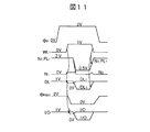
図1(a)から(c)は本発明の一実施例を示す図である。図1(a)はセル毎に、回路の動作電位点VCHとメモリセルの接続を制御する手段であるトランジスタQPを付加した例を示し、(b)は行毎にQPを付加した例、(c)はすべてのセルでQPを共有する例を示す。 FIGS. 1A to 1C are diagrams showing an embodiment of the present invention. FIG. 1A shows an example in which a transistor QP, which is a means for controlling the connection between the operating potential point VCH of the circuit and the memory cell, is added for each cell, and FIG. 1B shows an example in which QP is added for each row. c) shows an example in which QP is shared by all cells.
簡単のためメモリセル内のすべてのトランジスタのしきい電圧VTは0.5Vとする。したがってゲートとソースの電圧がほぼ等しければトランジスタにはサブスレッショルド電流は流れない。図1(a)は最も基本となる本発明の概念図である。メモリセルMCの高電位側の給電ノードであるPチャネルMOS QC1,QC2の共通ソースと、電源VCHの間にスイッチの働きをするPチャネルMOS QPがメモリセルに対して挿入される。メモリセルMCの低電位側の給電ノードであるNチャネルMOS QS1,QS2の共通ソースは基準電位VSS(通常は接地電位0V)に接続されている。ここで例示したメモリセルMCは、ゲートとドレインが互いに交差結合されたMOSトランジスタで構成されたスタティックメモリセルである。更に、詳しくはQC1とQS1からなるインバータと、QC2とQS2からなるインバータがあり、一方のインバータの出力が他方のインバータの入力にそれぞれ接続された記憶セルと、記憶ノードN1,N2にそれぞれその一端が接続された転送MOSトランジスタQT1、QT2からなる。このメモリセルMCの動作環境は、外部から供給される電圧VCCの十分に電流供給能力の高い電源があるものとし、VCCよりも電圧の高いVCHの電源は電流供給能力の低い電源であるとする。電流供給能力の低い電源ではその供給能力以上の電流が流れると一時的に電源の電圧が低下するという問題がある。 For simplicity, the threshold voltage VT of all transistors in the memory cell is 0.5V. Therefore, if the gate and source voltages are substantially equal, the subthreshold current does not flow through the transistor. FIG. 1A is a conceptual diagram of the present invention which is the most basic. A P-channel MOS QP that functions as a switch is inserted between the common source of the P-channel MOSs QC1 and QC2, which are power supply nodes on the high potential side of the memory cell MC, and the power source VCH. A common source of N channel MOSs QS1 and QS2 which are power supply nodes on the low potential side of the memory cell MC is connected to a reference potential VSS (usually a ground potential of 0 V). The memory cell MC illustrated here is a static memory cell composed of MOS transistors whose gates and drains are cross-coupled to each other. More specifically, there are an inverter composed of QC1 and QS1, and an inverter composed of QC2 and QS2. A storage cell in which the output of one inverter is connected to the input of the other inverter, and one end of each of the storage nodes N1 and N2 respectively. Are composed of transfer MOS transistors QT1 and QT2. As for the operating environment of this memory cell MC, it is assumed that there is a power source having a sufficiently high current supply capability of the voltage VCC supplied from the outside, and the power source of VCH having a voltage higher than VCC is a power source having a low current supply capability. . A power supply with a low current supply capability has a problem that the voltage of the power supply temporarily decreases when a current exceeding the supply capability flows.
メモリセルにデータ対線からデータを書き込む場合は、QPを非導通にした状態で通常は対線の一方にはVCCを、他方には0を印加する。この時ワード線電圧をVCCとすれば、記憶ノードN1,N2のいずれか一方にはQT1あるいはQT2のVTだけ降下したVCC−VTが、また他方には0が入力される。しかしこのままでは記憶電圧(ノードN1とN2の差電圧)はVCC−VTとなり、たとえばVCC=1V,VT=0.5Vでは0.5Vとなり低すぎる。そこで書き込んだ後、すなわちワード線電圧をオフにした後でQPを導通させ、共通ソースに十分高いVCH(例えば2V)を印加する。するとメモリセル内の交差結合トランジスタは差動アンプとして働くように活性化され、その結果として、N1,N2のいずれか一方はVCHまで充電され他方は0となる。結局記憶電圧はVCC−VTからVCHへと高くなる。QPを導通にするタイミングは、ワード線選択タイミングと一致されなくとも良いが、電流供給能力の弱い電源VCHからメモリセルを介してデータ線DL、/DLに不要な電流が流れないようにするためには、ワード線電圧をオフした後のタイミングとされることが望ましい。なお、ワード線をオフしてからQPを導通するまでの期間におけるノードN1、N2の書き込みデータは、ノードN1、N2のそれぞれが持つ寄生容量によって保持されることになる。上記のようにメモリセルを活性化した後のデータ保持期間や待機時にはQPをオンにしてメモリセルにVCHを給電しつづければ、この間のメモリセルの動作マージンは拡大する。またメモリセルの読み出し時にも動作は高速・安定である。QS1あるいはQS2の電流駆動能力がゲート電圧が高くなった分だけ向上するためである。このように書き込みはQPを非導通にした状態で行えるので、いかなる書き込みデータでもメモリセル内はダイナミック動作となり低電力で高速な書き込みができる。もしQPがなくメモリセルに直接 VCHが接続されていたり、書き込み途中でQPを導通させたりすると、それまで蓄えられていた記憶情報を反転させるような書き込みの場合に、QPを通して長時間電流が流れて高電力になったり反転させにくくなるなどの不都合が生じる。 When data is written to the memory cell from the data pair line, VCC is normally applied to one of the pair lines and 0 is applied to the other, with QP being non-conductive. At this time, if the word line voltage is set to VCC, VCC-VT lowered by VT of QT1 or QT2 is input to one of the storage nodes N1 and N2, and 0 is input to the other. However, the storage voltage (the difference voltage between the nodes N1 and N2) becomes VCC-VT if it remains as it is, for example, when VCC = 1V and VT = 0.5V, it becomes 0.5V, which is too low. Therefore, after writing, that is, after the word line voltage is turned off, QP is conducted, and a sufficiently high VCH (for example, 2 V) is applied to the common source. Then, the cross-coupled transistor in the memory cell is activated to act as a differential amplifier, and as a result, one of N1 and N2 is charged up to VCH and the other becomes zero. Eventually, the memory voltage increases from VCC-VT to VCH. The timing at which QP is turned on may not coincide with the word line selection timing, but in order to prevent unnecessary current from flowing from the power source VCH having a weak current supply capability to the data lines DL and / DL through the memory cell. It is desirable that the timing be after the word line voltage is turned off. Note that the write data of the nodes N1 and N2 in the period from when the word line is turned off to when QP is turned on is held by the parasitic capacitances of the nodes N1 and N2. If the QP is turned on and VCH is continuously supplied to the memory cell during the data holding period after activation of the memory cell or in the standby state as described above, the operation margin of the memory cell during this period is expanded. Also, the operation is fast and stable when reading from the memory cell. This is because the current driving capability of QS1 or QS2 is improved by the amount of increase in the gate voltage. Thus, since writing can be performed in a state where QP is non-conducting, any write data can be dynamically operated in the memory cell and can be written at low power and at high speed. If there is no QP and VCH is directly connected to the memory cell, or if QP is turned on in the middle of writing, a current flows for a long time through QP in the case of writing that reverses the stored information stored so far. Inconveniences such as high power and difficulty in reversing occur.
図1(b)は複数のメモリセルでQPを共有した実施例で、トランジスタ数が少なくなる分だけメモリセルは小形になる。今、MC1に前述したようにQP1を非導通にしたままで書き込むと、データ対線からMC1のたとえばQC1のゲートに0、QC2のゲートにはVCC−VT(0.5V)が強制的に加えられる。このためQC1が導通しそれまで共通給電線PL1の寄生容量に充電していたVCHはVCC−VTまで放電する。この時同じワード線WL1上のメモリセルMC2は実質的は読み出し動作が行われているが、上述したPL1の電圧低下でMC2の記憶情報が破壊されることはない。MC2の記憶電圧もそれまでのVCHからPL1の電圧であるVCC−VTに低下するだけである。メモリセル内の差動アンプの感度は対になるトランジスタのオフセット電圧などで決まりそれは例えば0.2V程度以下であり、VCC−VTがこの感度以上なので情報は破壊されない。すなわち書き込み終了後にQP1をオンにしてPL1に再びVCHを与えれば、MC2の記憶電圧もMC1と同様にVCHになる。この実施例では、選択されたワード線に対応する給電線1本だけをVCHに充電すればよい。ほかの多数の給電線(PL2など)はVCHのままなので、対応する充電トランジスタ(QP2)などをオンにしても充電動作は起こらない。つまり給電線の充電は局所化され、低電力化される。 FIG. 1B shows an embodiment in which QP is shared by a plurality of memory cells, and the memory cell becomes smaller as the number of transistors decreases. As described above, when QP1 is written in the non-conductive state as described above to MC1, 0 is applied to the gate of QC1 of MC1, for example, and VCC-VT (0.5V) is forcibly applied to the gate of QC2. It is done. Therefore, QC1 becomes conductive, and VCH that has been charged in the parasitic capacitance of the common power supply line PL1 is discharged to VCC-VT. At this time, the memory cell MC2 on the same word line WL1 is substantially subjected to a read operation, but the stored information of MC2 is not destroyed by the voltage drop of PL1 described above. The memory voltage of MC2 also only drops from the previous VCH to VCC-VT which is the voltage of PL1. The sensitivity of the differential amplifier in the memory cell is determined by the offset voltage of the paired transistors and the like, which is, for example, about 0.2 V or less, and information is not destroyed because VCC-VT is above this sensitivity. That is, if QP1 is turned on and VCH is again applied to PL1 after the writing is completed, the storage voltage of MC2 becomes VCH similarly to MC1. In this embodiment, only one power supply line corresponding to the selected word line needs to be charged to VCH. Since many other power supply lines (PL2 and the like) remain at VCH, charging operation does not occur even if the corresponding charging transistor (QP2) or the like is turned on. In other words, charging of the feeder line is localized and power consumption is reduced.
図1(c)は充電トランジスタQPを全てのメモリセルで共有した実施例で、集積度は上述した例よりも向上する。しかしこの場合は、非選択のワード線側のメモリセルの給電線を含む全ての給電線の電圧が降下してしまうので、それらをVCHまで充電するための充放電電力が増加したり低速になったりする可能性があるので注意を要する。尚、ワード線に対して隣り合う給電線を共通化するとメモリセルの面積を小さくできる。たとえば第1(b)において、PL1とPL2を共通な1本の給電線にしてこれを1個のトランジスタで制御すれば実効的にメモリセルの配線数が減るためである。 FIG. 1C shows an embodiment in which the charge transistor QP is shared by all the memory cells, and the degree of integration is improved from the above-described example. However, in this case, since the voltage of all the power supply lines including the power supply lines of the memory cells on the non-selected word line side drops, the charge / discharge power for charging them to VCH increases or becomes slow. It is necessary to be careful. It should be noted that the area of the memory cell can be reduced by sharing the power supply line adjacent to the word line. For example, in the first (b), if PL1 and PL2 are made one common power supply line and controlled by one transistor, the number of memory cell wirings is effectively reduced.
なお、SRAMのメモリセルの高電位側の給電ノードにスイッチMOSトランジスタを設ける回路構成は、特開昭60−38796号公報や特開平02−108297号公報に記載されるが、スイッチMOSを介して接続される電位は装置に供給される電源電位であり、本発明とはその思想が全く異なものである。 A circuit configuration in which a switch MOS transistor is provided at a power supply node on the high potential side of an SRAM memory cell is described in Japanese Patent Application Laid-Open Nos. 60-38796 and 02-108297. The connected potential is a power supply potential supplied to the device, and the idea is completely different from the present invention.
以下では主に図1(b)を例に、書き込み動作だけでなく読み出し動作を含めて、さらに具体的な実施例を説明する。 In the following, a more specific embodiment including not only the write operation but also the read operation will be described mainly using FIG. 1B as an example.
図3は本発明実施例の回路図で、図4は読みだし時のタイミング図、図5は書き込み時のタイミング図である。 FIG. 3 is a circuit diagram of the embodiment of the present invention, FIG. 4 is a timing diagram at the time of reading, and FIG. 5 is a timing diagram at the time of writing.
メモリセルとしてPチャネルMOSトランジスタとNチャネルMOSトランジスタから成るフリップフロップ型のセルを例にとり、セル内のすべてのトランジスタのしきい電圧VTは、サブスレッショルド電流がほぼ無視できる程度に高い値、たとえば0.5Vとする。また簡単のため4ビットのセルアレイを取り上げ、電池駆動でSRAMのVCC単一電源駆動を前提にVCC=1V,VCH=2Vと仮定している。本発明の特徴は、(1)セル給電線(PL1及びPL2)の電圧をセルの動作タイミングに応じて切り換えることにある。すなわちセルが非選択時の情報保持電圧(図3では2V)はセルの給電線から印加される電圧で決まり、その大きさはセルが選択時に該セルにデータ線から書き込まれる書き込み電圧よりも大きくなるようにセルの給電線の電圧が制御される。 Taking a flip-flop type cell composed of a P-channel MOS transistor and an N-channel MOS transistor as an example of the memory cell, the threshold voltage VT of all the transistors in the cell is high enough to make the subthreshold current almost negligible, for example 0 .5V. For the sake of simplicity, a 4-bit cell array is taken up, and it is assumed that VCC = 1V and VCH = 2V on the assumption that the battery is driven by a VCC single power source. The features of the present invention are (1) switching the voltage of the cell power supply lines (PL1 and PL2) according to the operation timing of the cell. That is, when the cell is not selected, the information holding voltage (2 V in FIG. 3) is determined by the voltage applied from the power supply line of the cell, and the magnitude is larger than the write voltage written to the cell from the data line when the cell is selected. Thus, the voltage of the feeder line of the cell is controlled.
(2)データ線(DL1,/DL1,DL2,/DL2)は、データ線の取り得る最大電圧(図3ではVCC=1V)のほぼ中間電圧(VCC/2=0.5V)を基準にして動作する。これによってデータ線の充放電電力が半減する。 (2) The data lines (DL1, / DL1, DL2, / DL2) are based on the intermediate voltage (VCC / 2 = 0.5V) of the maximum voltage (VCC = 1V in FIG. 3) that the data line can take. Operate. This halves the charge / discharge power of the data line.
(3)選択されたワード線のパルス電圧の振幅が、データ線の取り得る最大電圧よりも大きい。ワード線に接続された選択トランジスタのしきい電圧VTの影響をなくすために、該パルス電圧の振幅は、チップ内の昇圧回路などでデータ線の該最大電圧よりもVT以上の大きな値(VCH)に設定される。また昇圧された分だけQT1,QT2の電流駆動能力が向上し高速になる。 (3) The amplitude of the pulse voltage of the selected word line is larger than the maximum voltage that the data line can take. In order to eliminate the influence of the threshold voltage VT of the selection transistor connected to the word line, the amplitude of the pulse voltage is larger than the maximum voltage of the data line by a booster circuit in the chip (VCH). Set to Further, the current drive capability of QT1 and QT2 is improved by the boosted amount, and the speed is increased.
マイクロプロセッサチップなどに内蔵されるSRAMの部分、あるいはSRAMチップそのもの(以下、両者をまとめてSRAM)がSRAM活性化信号CEによって非活性化されている場合を考えてみよう。SRAM内の主要部はプリチャージ信号ΦPによってプリチャージ状態になっている。たとえばセルの給電線(PL1,PL2)は、外部電源電圧(VCC)をもとにしてチップ内部で十分昇圧された電圧VCHにプリチャージされている。セル内の微少なリーク電流によるセル内の記憶電圧の低下は、P−MOS QP1,QP2からの補償電流によって阻止され、これによって各セルの記憶状態は保持される。ここでVCHは電圧変換回路VC2で形成される。VC2はキャパシタを駆動するチャージポンプ回路を用いてチップ内部でVCCを昇圧して作られるようにされ、これに応じてその電流駆動能力は低い。しかしセル内のトランジスタのしきい電圧は0.5V以上と十分高く設定してあるので、メガビット級の大容量SRAMでもセルのリーク電流の合計はせいぜい10μA以下と十分低くすることが可能である。したがってVCH昇圧回路からすべてのメモリセルに補償電流は供給できる。尚、昇圧回路の詳細は、「超LSIメモリ(培風館,1994年11月発刊),ページ315」に述べられている。また本願の課題とする1V程度の非常に低電圧の電源VCCで動作するオンチップの昇圧回路については「1995 Symposium on VLSI Circuits Digest of Techincal Papers, (1995), pp.75-76」に記載される。この文献の昇圧回路に利用されるMOSトランジスタのしきい電圧は0.6V程度とされており、更にしきい電圧が低いMOSトランジスタを利用すれば更に低い電圧の電源電圧VCCでも動作する昇圧回路ができると考えられる。しきい電圧の低いトランジスタを利用する際には、前述したサブスレショルド電流に注意しなければならないが、昇圧回路を形成する程度のトランジスタの数であれば実用に耐えないほどのリーク電流とはならないようにすることが可能である。また、SRAMのメモリセルの高電位側の給電ノードに外部供給電源により昇圧電圧を発生する昇圧回路が接続される回路構成は、特開平6−223581号公報に記載されるが、前記給電ノードには昇圧回路の電位または外部供給電源が接続されるとしている。 Let us consider a case in which the SRAM portion incorporated in the microprocessor chip or the like, or the SRAM chip itself (hereinafter collectively referred to as SRAM) is inactivated by the SRAM activation signal CE. The main part in the SRAM is in a precharged state by a precharge signal ΦP. For example, the cell power supply lines (PL1, PL2) are precharged to a voltage VCH sufficiently boosted inside the chip based on the external power supply voltage (VCC). A decrease in the storage voltage in the cell due to a minute leak current in the cell is blocked by the compensation current from the P-MOSs QP1 and QP2, and thereby the storage state of each cell is maintained. Here, VCH is formed by the voltage conversion circuit VC2. VC2 is made by boosting VCC in the chip using a charge pump circuit for driving a capacitor, and its current driving capability is low accordingly. However, since the threshold voltage of the transistors in the cell is set to a sufficiently high value of 0.5 V or higher, the total leakage current of the cell can be sufficiently reduced to 10 μA or less at most even with a megabit class large capacity SRAM. Therefore, the compensation current can be supplied to all the memory cells from the VCH booster circuit. Details of the booster circuit are described in “VLSI LSI (Baifukan, published in November 1994), page 315”. The on-chip booster circuit that operates with a very low voltage power supply VCC of about 1V, which is the subject of this application, is described in “1995 Symposium on VLSI Circuits Digest of Techincal Papers, (1995), pp.75-76”. The The threshold voltage of the MOS transistor used in the booster circuit of this document is about 0.6 V. If a MOS transistor having a lower threshold voltage is used, a booster circuit that operates even at a lower power supply voltage VCC can be formed. it is conceivable that. When using a transistor with a low threshold voltage, attention must be paid to the above-mentioned subthreshold current. However, if the number of transistors is sufficient to form a booster circuit, the leakage current will not be practical enough. It is possible to do so. A circuit configuration in which a booster circuit for generating a boosted voltage by an external power supply is connected to a power supply node on the high potential side of an SRAM memory cell is described in JP-A-6-223581. Is connected to the potential of the booster circuit or an external power supply.
SRAM活性化信号CEによって非活性化されているプリチャージ期間には、それぞれのデータ線(DL1,/DL1,DL2,/DL2(この明細書では相補信号の対である反転信号は/DL1のように記述する。))はプリチャージ回路PCによりVCC/2にプリチャージされている。こうすることによってデータ線の電圧振幅は従来のVCCプリチャージに比べて半減するので、多ビットデータの同時書き込み時に従来から問題となっていたデータ線充放電電力を半減できる。この場合VCC/2電源は、VCCから電圧変換回路VC1で形成され、具体的には前述の「超LSIメモリ」の324頁の図4.60に記載される回路等が利用できる。このVCC/2は、チップ内部で作られるので一般に負荷電流駆動能力が低い。したがってプリチャージ時にこのVCC/2電源で直接データ対線の一方を0からVCC/2へとプリチャージすると、十分な充電電流が供給できなくなるのでVCC/2のレベルは変動してしまう。データ対線の数は通常64あるいは128以上と多数なので特にこの変動がおおきく問題となる。そこで各データ線にアンプAMPを設ける。アンプAMPの役割は、データ対線に現われたセル読み出し時の微少な差動電圧をVCCまで高速に増幅する。その結果、データ対線の一方は0となり他方はVCCとなる。次のプリチャージ動作ではQEQがオンとなりデータ対線は自動的に平衡化されVCC/2となる。このためVCC/2電源から大きな充電電流を流す必要はない。プリチャージ期間が長い場合にデータ対線がその微少リーク電流によって徐々にレベル変動するのを抑えるだけの微少電流を流せればよい。したがってAMPを使えば内蔵VCC/2電源回路が使える。 In the precharge period inactivated by the SRAM activation signal CE, each data line (DL1, / DL1, DL2, / DL2 (in this specification, the inverted signal which is a pair of complementary signals is like / DL1). )) Is precharged to VCC / 2 by the precharge circuit PC. By doing so, the voltage amplitude of the data line is halved compared to the conventional VCC precharge, so that it is possible to halve the data line charging / discharging power which has been a problem at the time of simultaneous writing of multi-bit data. In this case, the VCC / 2 power source is formed from the VCC to the voltage conversion circuit VC1. Specifically, the circuit described in FIG. 4.60 on page 324 of the above-mentioned “VLSI LSI” can be used. Since VCC / 2 is produced inside the chip, the load current driving capability is generally low. Therefore, if one of the data pair lines is precharged directly from 0 to VCC / 2 with this VCC / 2 power supply during precharge, a sufficient charge current cannot be supplied and the level of VCC / 2 will fluctuate. Since the number of data pairs is usually as large as 64 or 128 or more, this variation is a particularly serious problem. Therefore, an amplifier AMP is provided for each data line. The role of the amplifier AMP is to amplify a minute differential voltage at the time of cell reading appearing on the data pair line to VCC at high speed. As a result, one of the data pair lines becomes 0 and the other becomes VCC. In the next precharge operation, QEQ is turned on, and the data pair lines are automatically balanced to VCC / 2. Therefore, it is not necessary to flow a large charging current from the VCC / 2 power source. When the precharge period is long, it is only necessary to pass a minute current that suppresses the level fluctuation of the data pair line due to the minute leakage current. Therefore, if AMP is used, a built-in VCC / 2 power supply circuit can be used.
以下図4も参照しながらメモリセルからデータを読み出す場合について説明する。SRAMイネーブル信号CEによってSRAMが活性化され、あるワード線たとえばWL1が選択されWL1にVCHのパルスが印加されるとWL1上のすべてのセル(MC1,MC2)が活性化される。このワード線の選択信号パルスは行アドレス信号AXをうけて行アドレスデコーダXDEC・ドライバDRVにより形成される。今セルMC1内のノードN1,N2にそれぞれ0,2V(=VCH)が記憶されていると、QT1とQS1は導通するので、データ線DL1は0Vに向かって徐々に放電する。一方QS2とQC2のゲート電圧はほぼ0なので、QC2、QT2を通して電流が流れ、データ線DL1は0.5V(=VCC/2)からわずかに上昇する。データ対線に現われたこの微少な差動電圧が十分大きくなるには時間がかかるので、アンプAMPの駆動線SP,SNにパルスを印加してデータ線DL1,/DL1をそれぞれ0,1Vに高速に増幅する。AMPはセルほどにはSRAMの集積度やサブスレッショルド電流を決めないので、AMP内トランジスタの寸法はセル内のそれよりも大きく選べるし、そのしきい電圧も0.2V程度と低くできるので高速増幅が可能なのである。さらにAMPはアンプ駆動回路SPGによりメモリセルが選択状態とされるときに動作状態とされ、非動作状態(待機状態)では駆動線SPとSNは同電位にしておくのでサブスレッショルド電流が問題となることはない。またデータ対線電圧が0.5V程度でもAMPは動作する。 Hereinafter, a case where data is read from the memory cell will be described with reference to FIG. The SRAM is activated by the SRAM enable signal CE. When a certain word line, for example, WL1 is selected and a pulse of VCH is applied to WL1, all cells (MC1, MC2) on WL1 are activated. This word line selection signal pulse is generated by a row address decoder XDEC / driver DRV in response to a row address signal AX. If 0 and 2V (= VCH) are stored in the nodes N1 and N2 in the cell MC1, respectively, QT1 and QS1 become conductive, and the data line DL1 is gradually discharged toward 0V. On the other hand, since the gate voltages of QS2 and QC2 are almost zero, a current flows through QC2 and QT2, and the data line DL1 slightly rises from 0.5 V (= VCC / 2). Since it takes time for the minute differential voltage appearing on the data pair lines to be sufficiently large, a pulse is applied to the drive lines SP and SN of the amplifier AMP to amplify the data lines DL1 and / DL1 to 0 and 1 V, respectively, at high speed. To do. AMP does not determine the degree of SRAM integration and subthreshold current as much as the cell, so the size of the transistor in the AMP can be selected to be larger than that in the cell, and the threshold voltage can be lowered to about 0.2V, so high speed amplification. Is possible. Further, the AMP is activated when the memory cell is selected by the amplifier driving circuit SPG, and the drive lines SP and SN are kept at the same potential in the non-operating state (standby state), so that the subthreshold current becomes a problem. There is nothing. The AMP operates even when the data pair voltage is about 0.5V.
上記のようにして十分大きく増幅されたデータ対線の差電圧は、列アドレス・デコーダYDEC・ドライバDRVの読み出し選択信号ΦR1によってI/O対線上に出力され、読み出し・書き込み制御回路RWCを通りデータ出力DOUTとなる。ここでQR1,QR2はデータ対線の電圧を電流に変換する回路である。これらのトランジスタのしきい電圧を0.5Vとすると、データ線DL1の電圧は0VなのでI/0線には電流が流れず、一方/DL1では1Vなので/I/0線には電流が流れる。いずれに大きな電流が流れるかは、差動電流あるいは差動電圧(図中の抵抗Rを利用)の極性弁別の形でRWC内で検出できる。尚、QR1とQR2のしきい電圧VTが十分低い、たとえば0.2Vとすれば、アンプAMPで増幅する前の微少電圧差も検出できるようになるのでその分だけ高速になる。VTを低くした分だけ相互コンダクタンスが増加しより大きな電流を流せるためである。 The differential voltage of the data pair line amplified sufficiently large as described above is output onto the I / O pair line by the read selection signal ΦR1 of the column address decoder YDEC driver DRV, and passes through the read / write control circuit RWC for data Output DOUT. Here, QR1 and QR2 are circuits for converting the voltage of the data pair line into a current. When the threshold voltage of these transistors is 0.5V, the voltage of the data line DL1 is 0V, so that no current flows through the I / 0 line, while the current of / DL1 is 1V because it is 1V. Which large current flows can be detected in the RWC in the form of polarity discrimination of a differential current or a differential voltage (using the resistor R in the figure). If the threshold voltage VT of QR1 and QR2 is sufficiently low, for example, 0.2V, a minute voltage difference before amplification by the amplifier AMP can be detected, so that the speed is increased accordingly. This is because the mutual conductance increases as VT is lowered, and a larger current can flow.
以上の読み出し動作(図4)においてメモリセルMC1のノード電圧を詳細に調べてみよう。もしこの動作期間中にQP1やQP2を導通させたり、あるいはQP1やQP2を取り除いた構造にして給電線PL1などに強制にVCH(2V)を印加すると問題が出る。VCHが電流駆動能力の大きな外部電圧の場合には、PL1上のすべてのセルから大きな直流電流がワード線に電圧が印加されている期間中流れ続けるので大電力になってしまう。あるいは本実施例のように、チップ内で昇圧した電源電圧VCHを使う場合には、その昇圧回路の電流駆動能力が不足するのでVCHのレベルが低下する。このためPL1上の非選択セルの記憶電圧も低下する。いったんすべての給電線の電圧が低下するとVCHのレベル回復には長時間を要する。給電線の合計の寄生容量が大きいためである。このためSRAMのサイクル時間が遅くなる。そこでセル非活性時にはすべての給電線PL1,PL2をプリチャージ信号ΦPによって強制的にVCH(2V)にしておくが、活性化期間にはそれぞれの給電線をVCH発生回路から切り離す。各給電線はほぼフローティング状態となり、それらの寄生容量にVCHのレベルは保持される。しかしセルが活性化(この場合は読み出し動作)されると、結局はセルノードN1は0となり、QC2は強く導通する。これらトランジスタのソースはPL1に接続されているので、PL1のフローティング電圧はVCHから降下し、その結果としてN1,N2は高レベルに充電されようとする。しかし、N1は、強制的にDL1の電圧(0V)に固定されているので0のままである。一方QT2のゲート、すなわちWL1の電圧は2V,/DL1も1VなのでQT2は導通し、QC2によってPL1とN2の電圧が等しくなるまでN2は充電されつづけ、結局PL1は1Vになる。明らかに1Vに放電される給電線は局所化される。すなわちそれはPL1だけでほかの非選択ワード線に対応したPL2は放電されずにVCHのままである。実際のメモリでは多数の給電線が存在し、その中の1本しか放電されないからむだな充放電電力はなくなり、また内蔵されたVCH発生回路が充電すべき給電線は1本と局所化されるのでVCH発生回路の設計は容易となる。 Let us examine the node voltage of the memory cell MC1 in detail in the above read operation (FIG. 4). If QP1 or QP2 is made conductive during this operation period, or if QP1 or QP2 is removed and VCH (2V) is forcibly applied to the feeder line PL1 or the like, a problem arises. When VCH is an external voltage having a large current driving capability, a large DC current continues to flow from all cells on PL1 during the period in which the voltage is applied to the word line, resulting in a large power. Alternatively, when the power supply voltage VCH boosted in the chip is used as in this embodiment, the current driving capability of the boosting circuit is insufficient, and the level of VCH is lowered. For this reason, the storage voltage of the non-selected cells on PL1 also decreases. Once the voltage on all the feeder lines is reduced, it takes a long time to restore the VCH level. This is because the total parasitic capacitance of the power supply line is large. This slows down the SRAM cycle time. Therefore, when the cell is inactive, all the power supply lines PL1 and PL2 are forcibly set to VCH (2 V) by the precharge signal ΦP, but each power supply line is disconnected from the VCH generation circuit during the activation period. Each feeder line is almost in a floating state, and the level of VCH is held in their parasitic capacitance. However, when the cell is activated (in this case, the read operation), the cell node N1 eventually becomes 0 and QC2 is strongly conducted. Since the sources of these transistors are connected to PL1, the floating voltage of PL1 drops from VCH, and as a result, N1 and N2 tend to be charged to a high level. However, N1 remains 0 because it is forcibly fixed to the voltage of DL1 (0V). On the other hand, since the voltage of the gate of QT2, that is, WL1, is 2V and / DL1 is also 1V, QT2 is conductive, and N2 continues to be charged by QC2 until the voltages of PL1 and N2 become equal, and eventually PL1 becomes 1V. Obviously, the feeder line discharged to 1V is localized. That is, it is only PL1 and PL2 corresponding to other non-selected word lines is not discharged but remains VCH. In an actual memory, there are a large number of power supply lines, and only one of them is discharged, so there is no wasteful charging / discharging power, and the power supply line to be charged by the built-in VCH generation circuit is localized as one. Therefore, the design of the VCH generation circuit becomes easy.
セルMC1への書き込み動作は図5に示すように、共通I/O対線に差動電圧を印加して行う。今、MC1にそれまで記憶されている情報とは逆の情報を書き込む場合を例にとる。データ対線DL1,/DL1にはそれぞれ1V,0Vの電圧が印加され、この電圧がそのままセルノードN1,N2に印加される。したがってノードN1,N2には差電圧1Vが書き込まれたことになる。ワード線WL1を2Vから0へとオフにした後でΦPでプリチャージ動作を行うと、セルノードの差電圧1Vはセル自身の増幅作用によって2Vまで増幅される。セル給電線PL1の電圧は2Vになるからである。この高い電圧がその後の情報保持電圧となる。ここで書き込み動作においてもWL1をオフにし、VCH発生回路が充電すべき容量を最小にしてからPL1にVCHを印加しなければならない。
As shown in FIG. 5, the write operation to the cell MC1 is performed by applying a differential voltage to the common I / O pair. An example of writing information opposite to the information stored in MC1 is taken as an example. Voltages of 1V and 0V are applied to the data pair lines DL1 and / DL1, respectively, and these voltages are applied as they are to the cell nodes N1 and N2. Therefore, the
以上の動作によっても前述したように選択ワード線WL1上のほかのメモリセルMCの記憶情報が破壊されることはない。メモリセルMC1が読み出しあるは書き込み動作がなされてI/O対線と情報(データ)の授受を行っている間は、MC2のWL1には常に選択パルスが印加されるから図4と同様の読み出し動作がMC2とデータ対線DL2,/DL2の間で行われている。したがってPL1が2Vから1Vへ変わっても再び2VのVCHを印加するとMC2内の2つのノードはVCH,0へと復帰する。また非選択ワード線WL2上のメモリセルMC3,MC4の記憶情報にも全く悪影響はない。MC3,MC4内のトランジスタには、VTは十分高いのでサブスレッショルド電流は流れず、流れるとしても無視できるほど小さい接合リーク電流だけなので、給電線PL2はプリチャージ時のVCHが維持されるからである。 The above operation does not destroy the stored information of other memory cells MC on the selected word line WL1, as described above. While the memory cell MC1 is being read or written and the data (data) is exchanged with the I / O pair line, a selection pulse is always applied to WL1 of MC2, so that the same reading as in FIG. The operation is performed between MC2 and data pair lines DL2 and / DL2. Therefore, even if PL1 changes from 2V to 1V, if 2V VCH is applied again, the two nodes in MC2 return to VCH, 0. Further, there is no adverse effect on the stored information of the memory cells MC3 and MC4 on the unselected word line WL2. This is because the sub-threshold current does not flow through the transistors in MC3 and MC4, and the junction leakage current is negligibly small even if it flows, so that the power supply line PL2 maintains the VCH during precharge. .
選択ワード線のパルス電圧の振幅はVCCで、データ線の取り得る最大値(VD)をVCC−VT以下に設定すれば、ワード電圧を昇圧電源VCHから発生させずにすみ、またセル書き込み時などにメモリセル内トランジスタ(QT1,QT2)のしきい電圧VTの影響をなくせるので設計が容易になる。図6はその場合の実施例であり、(a)に回路図を、(b)に波形図を示す。図6は図3のSRAM全体のうちメモリセルの駆動方式に関係する部分を取り出したものであり、図3と比較したときの違いはプリチャージ回路PCと読み出し・書き込み回路RWCである。また、この実施例では、ワード線の信号レベルは基準電位である0Vと電源電位VCCにとり、非選択時のメモリセルの高電位側の給電ノードはVCH(=2VCC)、メモリセルの低電位側の給電ノードは基準電位である0Vとした。またデータ線のプリチャージ電位は、基準電位(0V=VSS)から少なくともメモリセルの感度電圧分だけ上昇した電位に設定したものである。 The amplitude of the pulse voltage of the selected word line is VCC, and if the maximum value (VD) that can be taken by the data line is set to VCC-VT or less, the word voltage does not need to be generated from the boost power supply VCH, or when writing to the cell Further, since the influence of the threshold voltage VT of the transistors (QT1, QT2) in the memory cell can be eliminated, the design becomes easy. FIG. 6 shows an embodiment in that case, where (a) shows a circuit diagram and (b) shows a waveform diagram. FIG. 6 shows a portion related to the driving method of the memory cell in the entire SRAM of FIG. 3, and the difference when compared with FIG. 3 is the precharge circuit PC and the read / write circuit RWC. In this embodiment, the signal level of the word line is set to the reference potential of 0 V and the power supply potential VCC, and the power supply node on the high potential side of the memory cell when not selected is VCH (= 2 VCC), and the low potential side of the memory cell. The power supply node was set to 0 V which is the reference potential. Further, the precharge potential of the data line is set to a potential that is increased by at least the sensitivity voltage of the memory cell from the reference potential (0 V = VSS).
メモリセルの感度電圧もしくは感度とは、例えば図1のDLと/DLの間に印加される電位差によって、フリップフロップ回路である記憶セルの状態を反転するために必要な最小の電位差である。データ線のDLと/DLの間に印加される電位差を感度電圧にするにはデータ線のプリチャージ電位はこの感度電圧の半分以上であれば良い。通常メモリセルの感度電圧は0.2Vより小さいためここでは余裕を持たせて参照電圧VRを0.2Vにとり、データ線のプリチャージ電位を0.2Vとした。言い換えればこの実施例は、データ線の取りうる電圧振幅の最大値をVT(0.5V)以下の、メモリセル自身がもつ感度電圧近くの低い電圧VRまで低くした例である。メモリセルのデータ線の電圧振幅は最小となるのでその分だけ高速で低電力動作ができる。またこのため図示するQL1とVRを参照電圧とするコンパレータから成る降圧電源でデータ対線をプリチャージできる。メモリセルの記憶電圧はVCH(2V)と十分高くできる。 The sensitivity voltage or sensitivity of the memory cell is the minimum potential difference necessary to invert the state of the memory cell that is a flip-flop circuit, for example, by the potential difference applied between DL and / DL in FIG. In order to make the potential difference applied between DL and / DL of the data line a sensitivity voltage, the precharge potential of the data line may be half or more of this sensitivity voltage. Since the sensitivity voltage of the normal memory cell is smaller than 0.2V, the reference voltage VR is set to 0.2V with a margin here, and the precharge potential of the data line is set to 0.2V. In other words, this embodiment is an example in which the maximum value of the voltage amplitude that can be taken by the data line is lowered to a low voltage VR which is lower than VT (0.5 V) and close to the sensitivity voltage of the memory cell itself. Since the voltage amplitude of the data line of the memory cell is minimized, the operation can be performed at higher speed and lower power accordingly. For this reason, the data pair lines can be precharged by a step-down power source composed of a comparator using QL1 and VR as reference voltages. The storage voltage of the memory cell can be made sufficiently high as VCH (2V).
以下図6(b)も参照しながら、読み出し動作について説明する。まずプリチャージ信号ΦPによってすべてのセル給電線はVCH(2V)にプリチャージされる。プリチャージ終了後、選択ワード線(WL1)に振幅VCC(1V)のパルスが印加される。セル内のノ−ドN1が0,N2がVCH(2V)の場合を例にとると、QT1は導通しデ−タ線DL1は0.2Vから0に向かって放電する。他方のデ−タ線/DL1は、QT2は導通するがQS2は非導通なのでノ−ドN2の電荷が/DL1に分配されデ−タ線はわずかに0.2Vから上昇しυとなる。この上昇分は、デ−タ線容量がセル内ノ−ド容量に比べて100倍以上と圧倒的に大きいのでわずかである。この時N2の電圧は2Vからυまで放電してしまう。このようにしてデ−タ対線に現われた差動電圧は、読みだしトランジスタQR1,QR2を通してセル読み出し情報としてI/O対線にとり出される。ここで大きな利得を得るためにQR1,QR2にはPチャンネルMOSが使われる。この一連の動作により、結局PL1はυまで低下してしまう。しかし次にプリチャ−ジ動作が始まると、υはセル自身の持つ感度よりも大きいので交差結合したPチャンネルMOSQC1とQC2によってVCHまで正常に増幅される。もし、N2とN1の電圧差υがこの感度以下なら、プリチャ−ジ時には正常には増幅されず、反転した情報が保持される恐れがある。尚、書き込み動作については、I/O対線から選択されたデ−タ対線の一方に0.2V、他方に0の差動電圧を印加した後に、読み出し動作と同様にプリチャージ動作によってPL1を2Vにすることによって行う。 Hereinafter, the read operation will be described with reference to FIG. First, all the cell power supply lines are precharged to VCH (2 V) by the precharge signal ΦP. After the precharge is completed, a pulse with an amplitude VCC (1 V) is applied to the selected word line (WL1). Taking the case where the node N1 in the cell is 0 and N2 is VCH (2V) as an example, QT1 is conducted and the data line DL1 is discharged from 0.2V toward 0. The other data line / DL1 conducts QT2 but does not conduct QS2, so that the charge of the node N2 is distributed to / DL1 and the data line slightly rises from 0.2 V to υ. This increase is slight because the data line capacity is overwhelmingly 100 times larger than the in-cell node capacity. At this time, the voltage of N2 is discharged from 2V to υ. The differential voltage appearing on the data pair line in this way is taken out to the I / O pair line as cell read information through the read transistors QR1 and QR2. Here, in order to obtain a large gain, a P-channel MOS is used for QR1 and QR2. As a result of this series of operations, PL1 eventually drops to υ. However, when precharge operation starts next, υ is larger than the sensitivity of the cell itself, so that it is normally amplified to VCH by the cross-coupled P-channel MOSs QC1 and QC2. If the voltage difference υ between N2 and N1 is less than this sensitivity, it will not be amplified normally during precharging, and inverted information may be retained. As for the write operation, after applying a differential voltage of 0.2 V to one of the data pair lines selected from the I / O pair line and 0 to the other, PL1 is applied by the precharge operation as in the read operation. Is set to 2V.
図7は、プリチャージ時にメモリセルの高電位側と低電位側の2つの給電ノードをパルス駆動することによって大きな記憶電圧を得る実施例であり、(a)にその回路図、(b)にその波形図を示す。図7は図3のSRAM全体のうちメモリセルの駆動方式に関係する部分を取り出したものであり、図3と比較したときの違いはメモリセルの低電位側の電位をメモリの選択非選択に応じて変化させられるようにしたことである。すなわち、メモリセルの低電位側の給電ノードは、非選択時には基準電位である0Vに、選択時にVCC/2から少なくとも前述したメモリセルの感度電圧分だけ降下した電位になるようにした。また、この実施例では、ワード線の信号レベルは基準電位である0Vと電源電位VCCにとり、データ線のプリチャージ電位はVCC/2、非選択時のメモリセルの高電位側の給電ノードはVCH(=2VCC)とした。 FIG. 7 shows an embodiment in which a large storage voltage is obtained by pulse driving the two power supply nodes on the high potential side and the low potential side of the memory cell during precharge. FIG. 7A is a circuit diagram thereof, and FIG. The waveform diagram is shown. FIG. 7 shows a portion related to the driving method of the memory cell in the entire SRAM of FIG. 3, and the difference when compared with FIG. 3 is that the potential on the low potential side of the memory cell is selected and not selected. That is, it can be changed accordingly. That is, the power supply node on the low potential side of the memory cell is set to the reference potential of 0 V when not selected, and to a potential that is lowered from VCC / 2 at least by the sensitivity voltage of the memory cell when selected. Further, in this embodiment, the signal level of the word line is set to the reference potential of 0 V and the power supply potential VCC, the precharge potential of the data line is VCC / 2, and the power supply node on the high potential side of the memory cell when not selected is VCH. (= 2 VCC).
図6では、データ線のプリチャージ電圧が0V付近の低い電圧だったのに対して、本実施例ではVCC/2であることに特徴がある。このため図6の読み出しトランジスタQR1,QR2を高速動作に適したNチャネルMOSで置き換えることもできる。またプリチャージ時の初期にセル内の2種類のアンプ(QS1とQS2,QC1とQC2)が活性化されるので、より高速に増幅される。今、VCH=3V,VCC=1.5V,VT=0.5V,VR=0.2Vと仮定しよう。また各データ対線には図3のようなVCC/2プリチャージ回路PCが接続されているものとする。プリチャージ期間はすべてのデータ線は0.75V,PL1などの給電線は3V,PL1’などのセル内のNチャネルMOSに接続されている給電線は0Vに設定される。プリチャージ期間はQL3によってQL2はカットオフになるので、QL4によってPL1’は0となるためである。またすべてのセル内の2つのノード(N1,N2)は記憶情報に応じて3Vあるいは0となっている。プリチャージが終了すると、PL1は3Vに保持される。一方PL1’は抵抗R’によってVCCに向かって上昇しはじめるが(VCC/2)−VR、つまり0.55Vになると(VCC/2)−VRを参照電圧とするコンパレータとQL2によって作られる電圧制限回路が作動しこれ以上の上昇は押さえられる。これとともにたとえば低電圧側のノードN1も0.55Vとなる。ここで消費電力を押さえるためにR’は比較的高い抵抗値に設定されるが、MOSトランジスタで代用することも可能である。ワード電圧が立ち上がると、N1が3VでN1が0.55VなのでQT1,QS1は導通しデータ線DL1は放電される。DL1とPL1’の間にはVRだけの差があるので、結局DL1はPL1’の電圧0.55Vまで放電される。一方QS2は非導通なので、前述したようにノードN2の電荷はQT2を通して/DL1に放電され、N2と/DL1はほぼ等しい電圧0.75V+υとなる。データ対線に現われたこの差電圧は各データ線に接続された読み出し回路の選択を通してI/O対線にとり出される。その後のプリチャージによってノードN1とN2間のほぼ0.2Vの差電圧は高速に3Vまで増幅される。PL1’が0になると、それまでN1は0.55VでN2は0.75Vよりわずか(υ)に高い電圧であったのでQS1とQS2の両者が導通し、N1とN2間のほぼ0.2Vの差電圧は交差結合形アンプQS1とQS2によって増幅される。またこの差電圧は、他の交差結合アンプQC1とQC2によっても増幅される。図6の例では、プリチャージ開始時のセル内での増幅初期にはQS1とQS2で構成されるアンプは非導通で、QC1とQC2で構成されるアンプだけで増幅したのでやや低速だった。しかし本例では増幅初期には両方のアンプが増幅作用に寄与するので高速である。また明らかに、書き込み動作は、選択されたデータ対線の一方に0.75V、他方に0.55Vと書き込みデータに応じて印加してやればよい。もちろんPL1’はセル選択時には読み出し時同様0.55Vになるように制御される。尚、本例ではデータ線の電圧振幅は0.2程度と極めて小さいので、チップに内蔵したVCC/2電圧発生回路でも駆動できる。したがって図3のアンプAMPは場合によっては取り除くこともできるのでチップが小形になる。またデータ対線は常にVCC/2近傍で動作するので、各データ線上のプリチャージ回路や読み出し回路(QR1,QR2)用トランジスタへのストレス電圧は半減するので信頼性は向上する。尚、データ線のプリチャージ電圧は必ずしもVCC/2である必要はない。明らかにデータ線のプリチャージ電圧を、選択時のPL1’電圧に対してセル内アンプの感度以上に高く設定すればよい。 In FIG. 6, the precharge voltage of the data line is a low voltage in the vicinity of 0V, whereas this embodiment is characterized in that it is VCC / 2. Therefore, the read transistors QR1 and QR2 in FIG. 6 can be replaced with an N-channel MOS suitable for high-speed operation. In addition, since two types of amplifiers (QS1 and QS2, QC1 and QC2) in the cell are activated at the early stage of precharge, they are amplified at a higher speed. Assume now that VCH = 3V, VCC = 1.5V, VT = 0.5V, VR = 0.2V. Further, it is assumed that a VCC / 2 precharge circuit PC as shown in FIG. 3 is connected to each data pair line. During the precharge period, all data lines are set to 0.75V, power supply lines such as PL1 are set to 3V, and power supply lines connected to N-channel MOS in the cell such as PL1 'are set to 0V. This is because in the precharge period, QL2 is cut off by QL3, and PL1 'becomes 0 by QL4. The two nodes (N1, N2) in all the cells are 3V or 0 depending on the stored information. When the precharge is completed, PL1 is held at 3V. On the other hand, PL1 'starts to rise toward VCC by the resistor R', but when it becomes (VCC / 2) -VR, that is, 0.55V, the voltage limit created by the comparator and QL2 using (VCC / 2) -VR as a reference voltage. The circuit is activated and any further rise is suppressed. At the same time, for example, the node N1 on the low voltage side becomes 0.55V. Here, in order to suppress power consumption, R ′ is set to a relatively high resistance value, but a MOS transistor can be substituted. When the word voltage rises, since N1 is 3V and N1 is 0.55V, QT1 and QS1 are conducted and the data line DL1 is discharged. Since there is a difference of VR between DL1 and PL1 ', DL1 is eventually discharged to a voltage of 0.55V at PL1'. On the other hand, since QS2 is non-conductive, the charge at node N2 is discharged to / DL1 through QT2 as described above, and N2 and / DL1 become substantially equal voltage 0.75 V + υ. This differential voltage appearing on the data pair line is taken out to the I / O pair line through selection of a read circuit connected to each data line. Subsequent precharging amplifies the difference voltage of approximately 0.2V between the nodes N1 and N2 to 3V at high speed. When PL1 'becomes 0, N1 was 0.55V and N2 was slightly higher than 0.75V (υ) until then, so both QS1 and QS2 became conductive, and approximately 0.2V between N1 and N2 Is amplified by the cross-coupled amplifiers QS1 and QS2. This differential voltage is also amplified by the other cross-coupled amplifiers QC1 and QC2. In the example of FIG. 6, the amplifier composed of QS1 and QS2 is non-conductive at the initial stage of amplification in the cell at the start of precharge, and is a little slow because it is amplified only by the amplifier composed of QC1 and QC2. However, in this example, both amplifiers contribute to the amplification action at the initial stage of amplification, so that the speed is high. Obviously, the write operation may be performed by applying 0.75 V to one of the selected data pair lines and 0.55 V to the other according to the write data. Of course, PL1 'is controlled to be 0.55V at the time of cell selection as in the case of reading. In this example, since the voltage amplitude of the data line is as small as about 0.2, it can be driven by a VCC / 2 voltage generating circuit built in the chip. Therefore, the amplifier AMP of FIG. 3 can be removed in some cases, so that the chip becomes small. Further, since the data pair line always operates in the vicinity of VCC / 2, the stress voltage to the precharge circuit and read circuit (QR1, QR2) transistors on each data line is halved, so that the reliability is improved. Note that the precharge voltage of the data line does not necessarily have to be VCC / 2. Obviously, the precharge voltage of the data line may be set higher than the sensitivity of the in-cell amplifier with respect to the PL1 'voltage at the time of selection.
また本実施例ではセル内NチャネルMOSのソース駆動線PL’(PL1’,PL2’)毎にQL2,QL3並びにコンパレータからなる電源回路を接続した例を示した。PL1’を0.55Vまで持ち上げる時間を速めてアクセス時間を高速にするためである。しかしチップ面積を小さくするためには図8に示すようにこの回路を他の給電線と共用することもできる。プリチャージ期間中には共通給電線PLCは共通電源回路によって常時(VCC/2)−VRに固定されているが、すべての給電線(PL1’・・・PLn’)は0である。今、PL1’が選択される場合には、外部アドレスによってデコードされてΦX1は0となりPL1’はPLCから切り離される。その後に/ΦPはVCCになりPL1を0に放電する。 Further, in this embodiment, an example is shown in which a power supply circuit composed of QL2, QL3 and a comparator is connected to each source drive line PL '(PL1', PL2 ') of the N-channel MOS in the cell. This is because the access time is increased by increasing the time for raising PL1 'to 0.55V. However, in order to reduce the chip area, this circuit can be shared with other feeder lines as shown in FIG. During the precharge period, the common power supply line PLC is always fixed to (VCC / 2) −VR by the common power supply circuit, but all the power supply lines (PL1 ′... PLn ′) are zero. Now, when PL1 'is selected, it is decoded by the external address, ΦX1 becomes 0, and PL1' is disconnected from the PLC. After that, / ΦP becomes VCC and PL1 is discharged to zero.
図9は読み出し時にデータ線の電圧がVCC近傍の値をとる駆動方式への適用例である。図9は図3のSRAM全体のうちメモリセルの駆動方式に関係する部分を取り出したものであり、図3と比較したときの違いはプリチャージ回路PCと読み出し・書き込み制御回路RWCである。この実施例では、ワード線の信号レベルは基準電位である0Vと電源電位VCCにとり、非選択時のメモリセルの高電位側の給電ノードはVCH(=2VCC)、メモリセルの低電位側の給電ノードは基準電位である0Vとした。またデータ線のプリチャージ電位をVCCにした。 FIG. 9 shows an example applied to a driving method in which the voltage of the data line takes a value near VCC at the time of reading. FIG. 9 shows a portion related to the driving method of the memory cell in the entire SRAM of FIG. 3, and the difference when compared with FIG. 3 is the precharge circuit PC and the read / write control circuit RWC. In this embodiment, the signal level of the word line is set to 0 V which is the reference potential and the power supply potential VCC, the power supply node on the high potential side of the memory cell when not selected is VCH (= 2 VCC), and the power supply on the low potential side of the memory cell. The node was set to a reference potential of 0V. The precharge potential of the data line was set to VCC.
各データ線には、選択されたセルに対して負荷となるトランジスタQD1とQD2並びにデータ対線電圧を平衡化するトランジスタQEQが接続されている。これらの回路がこの実施例のプリチャージ回路PCである。図10の読み出し動作タイミングを用いて以下に動作を説明する。 Each data line is connected to transistors QD1 and QD2 which are loads for the selected cell, and a transistor QEQ which balances the data line voltage. These circuits are the precharge circuit PC of this embodiment. The operation will be described below using the read operation timing of FIG.
プリチャージ期間には、データ対線はVCC(1V)、PL1はVCH(2V)である。ここで、データ対線DL1,/DL1が列アドレス選択信号ΦRW1によって選択され(ΦRW1が1Vから0)、またワード線WL1が選択され0から1Vのパルスが印加されたとする。N2が2Vとすると、QD1,QT1,QS1の間に直流電流が流れその結果DL1には微少なレシオ電圧VS(約0.2V)が現われる。一方N1はほぼ0でQS2は非導通で、またQT2もその電圧関係から明らかなように非導通なのでQD2,QT2,QS2の経路に電流が流れることはない。なぜならN1の電圧はレシオ動作によって多少もち上がるが、それはVT以下になるようにセル内のトランジスタの大きさが設計されているためである。したがってデータ対線にはVSだけの差動信号が現われる。この電圧はレシオ電圧なので図3のような複雑な読み出し回路を経なくても、そのままI/O対線に伝えられ外部に読み出される。ここで QS2とQT2は常に非導通なのでN2のノードに蓄積されていた電荷は消失されることはない。つまりPL1の電圧は2Vのままである。したがってチップに内蔵したVCH昇圧回路の電流駆動能力がそれほどなくても、その負荷となるPL1に電流が流れないから、場合によってはQp1を取り除き直接接続することも可能である。しかしこれができるのは読み出し動作に限られる。書き込み動作ではこれが困難になることを図11をもとに説明する。 During the precharge period, the data pair line is VCC (1V) and PL1 is VCH (2V). Here, it is assumed that the data pair lines DL1, / DL1 are selected by the column address selection signal ΦRW1 (ΦRW1 is 1V to 0), the word line WL1 is selected, and a pulse of 0 to 1V is applied. If N2 is 2V, a direct current flows between QD1, QT1, and QS1, and as a result, a very small ratio voltage VS (about 0.2V) appears in DL1. On the other hand, N1 is almost 0, QS2 is non-conductive, and QT2 is non-conductive as apparent from the voltage relationship, so that no current flows through the paths QD2, QT2, and QS2. This is because the voltage of N1 slightly rises due to the ratio operation, because the size of the transistor in the cell is designed to be lower than VT. Therefore, a differential signal of only VS appears on the data pair line. Since this voltage is a ratio voltage, even if it does not go through a complicated readout circuit as shown in FIG. Here, since QS2 and QT2 are always non-conductive, the charge accumulated in the node of N2 is not lost. That is, the voltage of PL1 remains 2V. Therefore, even if the current drive capability of the VCH booster circuit built in the chip is not so much, no current flows through PL1 serving as a load. Therefore, in some cases, Qp1 can be removed and directly connected. However, this can only be done with a read operation. The fact that this is difficult in the write operation will be described with reference to FIG.
I/O対線からデータ対線の一方DL1に1Vが、他の一方/DL1に0Vになるような書き込みが行われると、セル内のノードN1はそれまでのほぼ0から0.5Vになる。QT1のしきい電圧は0.5Vで、WL1の電圧は1Vなのでしきい電圧分だけ降下した電圧がN1の電圧になるからである。一方N2はそれまでの2Vから0となる。QT2が導通しN2は/DL1の電圧に等しくなるように放電するためである。このためQC1はQC2に比べて導通の度合いが強くなり、フローティング状態のPL1は強制的にデータ線からN1に与えられている0.5Vに放電してしまう。したがって後続のプリチャージによってPL1を再び2Vになるように充電しなければならない。 When writing is performed so that 1V is applied to one DL1 of the data pair line from the I / O pair line and 0V is applied to the other one / DL1, the node N1 in the cell is changed from almost 0 to 0.5V. . This is because the threshold voltage of QT1 is 0.5V and the voltage of WL1 is 1V, so that the voltage dropped by the threshold voltage becomes the voltage of N1. On the other hand, N2 becomes 0 from the previous 2V. This is because QT2 conducts and N2 discharges to be equal to the voltage of / DL1. For this reason, QC1 is more conductive than QC2, and PL1 in the floating state is forcibly discharged from the data line to 0.5 V applied to N1. Therefore, PL1 must be charged again to 2V by the subsequent precharge.
PL1の電圧降下が大きければ昇圧電圧(VCH)発生回路でそれに応じた電荷をPL1に供給しなければならないので昇圧回路の負担が重くなる。このためVCH発生回路自体の面積が大きくなったり消費電力が大きくなったりする。図12はその電圧降下をVCC近傍までに抑えるための負荷回路である。図12(a)ではセルが選択される時間帯ではQPを非導通にし、代わりにQRを導通させる。給電線の電圧はVCHからVCCになるので、セル内ノードの一方(たとえばN1)は図11のように0.5Vまで降下することはなくVCC(1V)に抑えられる。図12(b)ではプリチャージパルス/ΦPを取り除き設計を簡単にしたものである。しきい電圧が0.2V程度と他のトランジスタのそれよりも低いNチャネルMOS QRが使われている。ダイオード接続されているので、給電線の電圧がVCC−VT、つまり0.8V以下になると導通するので、それ以下の電圧降下を防ぐことができる。つまりセルノードの一方は図11のように0.5Vまで降下することはなく0.8Vに抑えられる。このトランジスタQRはQpが長時間オフのパルスタイミングの場合に、フローティング状態にあるPL1の電圧レベルが、セル内の拡散層リーク電流によって低下しすぎるのを防ぎ、セルの電圧マージンを拡大する役割もする。 If the voltage drop of PL1 is large, the boosted voltage (VCH) generation circuit must supply charges corresponding to it to PL1, so the burden on the booster circuit becomes heavy. For this reason, the area of the VCH generating circuit itself increases and the power consumption increases. FIG. 12 shows a load circuit for suppressing the voltage drop to near VCC. In FIG. 12A, QP is made non-conductive in the time zone when the cell is selected, and QR is made conductive instead. Since the voltage of the power supply line is changed from VCH to VCC, one of the nodes in the cell (for example, N1) does not drop to 0.5V as shown in FIG. 11, and is suppressed to VCC (1V). In FIG. 12B, the precharge pulse / ΦP is removed and the design is simplified. An N channel MOS QR is used which has a threshold voltage of about 0.2 V, which is lower than that of other transistors. Since it is diode-connected, it conducts when the voltage of the feeder line is VCC-VT, that is, 0.8 V or less, so that a voltage drop below that can be prevented. That is, one of the cell nodes does not drop to 0.5V as shown in FIG. This transistor QR also prevents the voltage level of PL1, which is in a floating state, from being lowered too much by the diffusion layer leakage current in the cell and expands the cell voltage margin when Qp is off for a long time. To do.
図10、図11の電圧印加を前提にすると、図9のようにワード線と給電線を平行に設置した構成以外に、図13のようにワード線WL1,WL2と給電線PL1,PL2を直交に配置した構成もとれる。たとえばWL1上のセルが読み出された場合、それらすべてのセルは図10と同様な動作を行うのですべての給電線の電圧(VCH)レベルは変わらない。しかし書き込み動作では選択されたデータ対線に属する給電線だけが変化する。たとえばデータ対線DL1,/DL1(図中では明らかなので省略)に書き込み情報に対応した1Vと0の組合せのパルス電圧を印加すると、セルMC1は図11と同様な動作を行うのでPL1の電圧は2Vから0.5Vまで降下してしまう。セルMC2は図10と同様な動作を行うのでPL2の電圧VCHは変わらない。ワード線と給電線の相互の配置関係を平行にするか直交にするかはセルのレイアウトと面積に依存する。図9では給電線とデータ対線は交差するので異なる配線層でレイアウトしなければならない欠点はあるが、低雑音という利点がある。たとえばWL1にパルスが印加されセルMC1が書き込まれたために大きな電圧変化がPL1に起こった場合を考えてみよう。この時セルMC2は実効的には読み出し動作が行われているので、その信号がデータ対線DL2,/DL2に現われている。この信号は微少なのでMC2の動作は雑音に強く影響を受けやすい。しかしデータ対線はPL1と直交しているので、PL1の電圧変化が結合容量を介して発生する雑音はデータ対線上では相殺されてしまう。図13は、図9とは利害得失が逆になる。たとえばPL1の電圧変動によって隣接するデータ対線(DL2,/DL2)には差動雑音が発生する。しかしこの場合には、ダイナミックメモリなどでよく知られているようにデータ対線を途中で対線間交差すれば雑音は相殺できる。 Assuming voltage application in FIGS. 10 and 11, the word lines WL1 and WL2 and the feed lines PL1 and PL2 are orthogonal to each other as shown in FIG. 13 in addition to the configuration in which the word lines and the feed lines are installed in parallel as shown in FIG. The configuration placed in can be taken. For example, when cells on WL1 are read, all the cells perform the same operation as in FIG. 10, and therefore the voltage (VCH) levels of all the feeder lines do not change. However, in the write operation, only the power supply line belonging to the selected data pair line changes. For example, when a pulse voltage of a combination of 1V and 0 corresponding to the write information is applied to the data pair lines DL1, / DL1 (not shown in the figure), the cell MC1 operates in the same manner as in FIG. It drops from 2V to 0.5V. Since the cell MC2 performs the same operation as in FIG. 10, the voltage VCH of PL2 does not change. Whether the mutual arrangement of the word lines and the feeder lines is parallel or orthogonal depends on the layout and area of the cell. In FIG. 9, since the feeder line and the data pair line cross each other, there is a disadvantage that the wiring layer must be laid out in different wiring layers, but there is an advantage of low noise. For example, consider a case where a large voltage change occurs in PL1 because a pulse is applied to WL1 and cell MC1 is written. At this time, since the read operation is effectively performed on the cell MC2, the signal appears on the data pair lines DL2 and / DL2. Since this signal is very small, the operation of MC2 is strongly affected by noise and easily affected. However, since the data pair line is orthogonal to PL1, the noise generated by the voltage change of PL1 through the coupling capacitance is canceled on the data pair line. FIG. 13 is contrary to FIG. 9 in terms of interests. For example, differential noise is generated in adjacent data pair lines (DL2, / DL2) due to voltage fluctuation of PL1. However, in this case, as is well known in dynamic memory, noise can be canceled by crossing the pair of data along the way.
以上の実施例ではVCHはチップ内でVCCを昇圧した電源から発生させることを前提としてきた。これはユーザにとって使い易いVCC単一電源動作を実現するためである。しかし場合によってはVCHはチップ外部電源そのものでもよい。たとえば図14のように、外部2電源(VCC1,VCC2)の場合が考えられる。チップは入出力インタフェース回路INTFとスタティックメモリSRAMや演算回路(たとえばマイクロプロセッサMPU)などのコアCOREからなるとする。INTFは既存の論理インタフェースレベルを保証するために比較的寸法の大きな素子を比較的高い電圧(VCC1)で動作させる。一方COREはチップの性能(速度、電力)やチップ面積を決定するので、この部分の主要部は低い電圧(VCC2)で動作する微細素子を用いて高性能化する。CORE内の素子は一般にはINTF内の素子より微細である。このようなチップでは、VCC1をこれまでの実施例内のVCHとみなせばよい。こうすることによってチップ全体としては2電源動作だが、内部電源動作に伴う出力レベル変動などの問題がなくなり設計が容易になる。図15は図14を単一電源で実現したチップへの適用例である。COREの主要部を、外部単一電源(VCC1)を降圧した内部電源(VCC2)で動作させたチップにおいて、VCC1をこれまでの実施例内のVCHとみなせばよい。 In the above embodiments, VCH has been premised on being generated from a power source obtained by boosting VCC in the chip. This is to realize a VCC single power supply operation that is easy for the user to use. However, in some cases, VCH may be the chip external power supply itself. For example, as shown in FIG. 14, the case of two external power sources (VCC1 and VCC2) can be considered. The chip includes an input / output interface circuit INTF and a core CORE such as a static memory SRAM and an arithmetic circuit (for example, a microprocessor MPU). INTF operates a relatively large element at a relatively high voltage (VCC1) to ensure the existing logic interface level. On the other hand, since CORE determines chip performance (speed, power) and chip area, the main part of this part is improved in performance by using fine elements that operate at a low voltage (VCC2). The elements in CORE are generally finer than the elements in INTF. In such a chip, VCC1 may be regarded as VCH in the previous embodiments. In this way, the entire chip operates with two power supplies, but problems such as output level fluctuations associated with the internal power supply operations are eliminated, and the design is facilitated. FIG. 15 shows an application example to a chip in which FIG. 14 is realized by a single power source. In a chip in which the main part of CORE is operated by an internal power supply (VCC2) obtained by stepping down an external single power supply (VCC1), VCC1 may be regarded as VCH in the above embodiments.
以上の実施例ではメモリセルはCMOS形を仮定したが、本発明ではメモリセル内の差動アンプ機能を応用しているので、メモリセル内に交差結合したラッチ形アンプが少なくても1個あればよい。PチャネルMOS(QC1,QC2)の代わりに、よく知られた高抵抗ポリシリコン負荷などでもよい。ノードN1,N2をVCHに向けて持ち上げられるので結局は交差結合したNチャネルMOS(QS1,QS2)で増幅できるようになるからである。またメモリセル内の転送(トランスファー)機能を持つNチャネル転送トランジスタQT1,QT2のVTはメモリセル内のほかのトランジスタのVTよりも低く、たとえば0.2にしてもよい。選択時にVTを低くした分だけQT1,QT2の実効ゲート電圧が増加し駆動電流が増えて高速動作が可能になる。ただし非選択時にQT1あるいはQT2を通してサブスレッショルド電流が流れるのでこれをなくすために、非選択状態でのワード線すなわちQT1,QT2のゲートをこれまでの0から負電圧たとえば−0.2Vより深くなるようにバイアスしなければならない。ゲート電圧とソース電圧をそれぞれVG,VSとすれば、QT1あるいはQT2の非選択時の実効ゲート電圧はVG−VS−VTとなるが、VG,VS,VTがそれぞれ−0.2V以下、0、0.2Vではこの実効ゲート電圧は−0.4V以下となる。一方、サブスレッショルド電流が無視できるVTの最小値を0.4Vとすれば、通常のバイアス条件で0.4VのVTを持つトランジスタの実効ゲート電圧は、VG,VS,VTがそれぞれ0,0,0.4Vなので、−0.4Vとなる。したがって上述した低いVTと負電圧ゲートを組み合わせた方式ではより低い実効ゲート電圧が加わるのでサブスレッショルド電流は流れない。尚、この場合選択ワード電圧は、非選択状態の−0.2VからVCCあるいはそれ以上に立ち上がるパルスとなる。 In the above embodiment, the memory cell is assumed to be a CMOS type. However, since the present invention applies the differential amplifier function in the memory cell, there is at least one latch type amplifier that is cross-coupled in the memory cell. That's fine. Instead of the P-channel MOS (QC1, QC2), a well-known high resistance polysilicon load may be used. This is because the nodes N1 and N2 can be lifted toward VCH, so that they can eventually be amplified by cross-coupled N-channel MOSs (QS1 and QS2). Further, the VT of the N-channel transfer transistors QT1 and QT2 having a transfer (transfer) function in the memory cell is lower than the VT of other transistors in the memory cell, and may be 0.2, for example. The effective gate voltage of QT1 and QT2 is increased by the amount that VT is lowered at the time of selection, and the drive current is increased to enable high-speed operation. However, since the subthreshold current flows through QT1 or QT2 when not selected, the word lines in the unselected state, that is, the gates of QT1 and QT2 are made deeper than the negative voltage, for example, −0.2 V, from 0 so far. Must be biased. If the gate voltage and the source voltage are VG and VS, respectively, the effective gate voltage when QT1 or QT2 is not selected is VG−VS−VT, but VG, VS and VT are −0.2V or less, 0, At 0.2V, this effective gate voltage is −0.4V or less. On the other hand, if the minimum value of VT at which the sub-threshold current can be ignored is 0.4 V, the effective gate voltage of a transistor having VT of 0.4 V under normal bias conditions is 0, 0, VG, VS, VT respectively. Since it is 0.4V, it becomes -0.4V. Therefore, in the above-described method combining the low VT and the negative voltage gate, a lower effective gate voltage is applied, so that the subthreshold current does not flow. In this case, the selected word voltage is a pulse rising from -0.2 V in the non-selected state to VCC or higher.
またこれまではメモリセル内のPチャネルとNチャネルトランジスタのVTを0.5Vと等しいものと仮定してきたが、必ずしもその必要はない。Nチャネルトランジスタはデータ線への読み出し電流などを決定する重要なトランジスタなので、このVTはサブスレッショルド電流が問題にならない程度のできるだけ低いVTたとえば0.4Vにする。しかしPチャネルトランジスタはメモリセル内の微少容量を充電するのが主な役割で多少低速でもかまわないので、その絶対値は0.4V以上たとえば0.6Vに設定してもよい。また簡単のためVCHはVCCの2倍と仮定してきたが、VCHはトランジスタの耐圧、たとえばゲート耐圧以下である限り、VCC以上であればよい。 In the past, it has been assumed that VT of the P-channel and N-channel transistors in the memory cell is equal to 0.5 V, but this is not always necessary. Since the N-channel transistor is an important transistor that determines the read current to the data line, this VT is set to a VT as low as possible, for example, 0.4 V so that the subthreshold current does not become a problem. However, since the P-channel transistor has a main role of charging a minute capacity in the memory cell and may be a little slow, its absolute value may be set to 0.4V or more, for example, 0.6V. Further, for the sake of simplicity, it has been assumed that VCH is twice VCC, but VCH may be equal to or higher than VCC as long as it is lower than the breakdown voltage of the transistor, for example, the gate breakdown voltage.
さらにメモリセル内の感度を高めたままで高速に給電線を充電する方法もある。前述したようにメモリセル内でトランジスタが交差結合した回路は差動アンプとみなせるが、オフセット電圧以外にノードN1、N2間の容量差も差動アンプの感度に影響する。メモリセルのレイアウトによっては、高密度化を優先にすると容量差ができる場合があるが、この値が大きいと感度が悪くなる。つまり増幅直前にはノードN1,N2の間により大きな電圧差が必要になる。この容量差による感度は、給電線(たとえばPL1)をVCHに立ち上げる速度が速いほど悪くなる。この問題は図16に示すような2段増幅で解決できる。すなわちそれぞれの給電線(PL1など)に互いにチャネル幅の大幅に異なる(たとえば10倍)2個のトランジスタを並列接続する。ΦPを印加してまずチャネル幅の小さいトランジスタ(QP1)を導通して給電線を少しずつ充電し、ノードN1,N2間がある大きな電圧差まで増幅されてからΦP’を印加してチャネル幅の大きなトランジスタ(QP1’)を導通して高速に充電する。 There is also a method of charging the power supply line at a high speed while increasing the sensitivity in the memory cell. As described above, a circuit in which transistors are cross-coupled in a memory cell can be regarded as a differential amplifier. In addition to the offset voltage, a capacitance difference between nodes N1 and N2 also affects the sensitivity of the differential amplifier. Depending on the layout of the memory cell, there may be a difference in capacity when priority is given to high density, but if this value is large, the sensitivity will deteriorate. That is, a larger voltage difference is required between the nodes N1 and N2 immediately before amplification. The sensitivity due to this capacitance difference becomes worse as the speed at which the feed line (for example, PL1) is raised to VCH is faster. This problem can be solved by two-stage amplification as shown in FIG. That is, two transistors whose channel widths are significantly different (for example, 10 times) from each other are connected in parallel to each power supply line (PL1 or the like). Applying ΦP, the transistor with a small channel width (QP1) is turned on to charge the power supply line little by little. After amplification to a large voltage difference between the nodes N1 and N2, ΦP 'is applied to A large transistor (QP1 ') is turned on to charge at high speed.
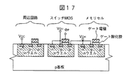
図17は本発明の実施例の断面図である。本実施例に示すように、スイッチMOS(QP)とメモリセルのPMOSトランジスタはnウエルに形成されているが、それぞれのトランジスタのソースまたはドレイン電極はVCHまで大きくなるためにそれらのウエルの電位もVCHにしておく必要がある。また、このとき周辺回路のPMOSトランジスタを作るnウエルの電位はVCCにする場合には基板をP型にしておけばよい。 FIG. 17 is a cross-sectional view of an embodiment of the present invention. As shown in this embodiment, the switch MOS (QP) and the PMOS transistor of the memory cell are formed in an n-well. However, since the source or drain electrode of each transistor is increased to VCH, the potential of these wells is also increased. It is necessary to keep VCH. At this time, if the potential of the n-well forming the PMOS transistor of the peripheral circuit is set to VCC, the substrate may be made P-type.
図18は本発明の別の断面図の実施例である。本実施例では、スイッチMOSとメモリセルのPMOSトランジスタには大きい電圧VCHがかかるため、これらのMOSのゲート酸化膜を周辺回路よりも厚くすることによって耐圧を大きくしたものである。周辺回路のMOSトランジスタは、酸化膜圧が薄いままなのでトランスコンダクタンスが大きくなり、高速に動作できる効果がある。 FIG. 18 is another cross-sectional embodiment of the present invention. In this embodiment, since a large voltage VCH is applied to the switch MOS and the PMOS transistor of the memory cell, the breakdown voltage is increased by making the gate oxide film of these MOSs thicker than the peripheral circuit. The MOS transistor in the peripheral circuit has an effect that the transconductance increases because the oxide film pressure remains thin, and it can operate at high speed.
図19は本発明の別の実施例の断面図である。本実施例では、図1の(a)に示すように、スイッチMOSが各メモリセルに付いている時のようにスイッチMOSとメモリセルのPMOSが分離しない場合の実施例である。このような場合には両MOSトランジスタを形成するウエルをVCHの電位にしておけばよい。 FIG. 19 is a cross-sectional view of another embodiment of the present invention. In this embodiment, as shown in FIG. 1A, the switch MOS and the memory cell PMOS are not separated as in the case where the switch MOS is attached to each memory cell. In such a case, the well in which both MOS transistors are formed should be set to the potential of VCH.
図20は本発明の別の実施例の断面図で、本発明をN型基板上に形成した場合の実施例である。N型基板上に本発明を適用する場合、周辺回路とスイッチMOSとメモリセルのPMOSを分離できない。したがって、本実施例に示すようにスイッチMOSとメモリセルのPMOSには共通の深いPウエルを形成し、その中にNウエルを形成して周辺回路と電位を変えるようにできる。 FIG. 20 is a cross-sectional view of another embodiment of the present invention, in which the present invention is formed on an N-type substrate. When the present invention is applied to an N-type substrate, the peripheral circuit, the switch MOS, and the PMOS of the memory cell cannot be separated. Accordingly, as shown in the present embodiment, a common deep P well can be formed in the switch MOS and the PMOS of the memory cell, and an N well can be formed therein to change the potential of the peripheral circuit.
本発明の良さを最大限に活かすには、メモリアレイと周辺回路にさらなる工夫があることが望ましい。図21はチップ内のSRAM部分または、1チップのSRAMに適用したその実施例である。メモリ部分は、複数のメモリアレイ(MA1,MA2,…)に分割されている。グローバルワード線は複数のメモリアレイにまたがって布線されている。メモリアレイ内では、サブワード線(WL11,…,WLn1,WL12,…,WLn2,…)方向にm個、データ線方向(DL11,/DL11,…,DL12,/DL12,…,…)にn個、マトリクス配置されたm×n個の複数のメモリセルMCから成る。スイッチMOSトランジスタ(QPL11,…,QPLn1,QPL12,…,QPLn2,…)を介して複数のメモリセルの高電位側への給電ノードに昇圧電圧VCHが印加されるサブ給電線(PL11,,…,PLn1,PL12,…,PLn2,…)はそれぞれ前述したサブワード線と対をなすように布線されている。尚、サブワード線は、前述した実施例との対応では単にワード線と読み換えることができる。 In order to make the best use of the present invention, it is desirable that the memory array and the peripheral circuit be further devised. FIG. 21 shows an embodiment in which the present invention is applied to an SRAM portion in a chip or a one-chip SRAM. The memory portion is divided into a plurality of memory arrays (MA1, MA2,...). Global word lines are wired across a plurality of memory arrays. In the memory array, m in the direction of sub-word lines (WL11,..., WLn1, WL12,..., WLn2,...) And n in the data line directions (DL11, / DL11,. , Composed of a plurality of m × n memory cells MC arranged in a matrix. Sub-feed lines (PL11,..., To which the boosted voltage VCH is applied to power supply nodes to the high potential side of the plurality of memory cells via switch MOS transistors (QPL11,..., QPLn1, QPL12,. PLn1, PL12,..., PLn2,... Are wired so as to be paired with the sub-word lines described above. The sub word line can be simply read as a word line in correspondence with the above-described embodiment.
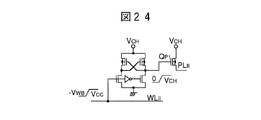
今、図9を基本とする方式で、図22に示すようにメモリセルMCの記憶セルを形成するMOSトランジスタ(QC1,QC2,QS1,QS2)のVTは0.5V、転送MOSトランジスタ(QT1,QT2)のVTは0.2Vとする。すなわち記憶セルに含まれるMOSトランジスタは、SRAM全体としてサブスレッショルド電流が問題とならないしきい電圧に設定されており、逆に転送MOSトランジスタは注意を要するしきい電圧に設定されている。またこのSRAMに外部から供給される電源VCCは1V、このVCCから電圧変換回路VC2で形成された昇圧電圧VCHは2V(=2VCC)、同じくVCCから電圧変換回路VC3で形成された負電圧−VWBは0.2Vとした。 Now, in the system based on FIG. 9, as shown in FIG. 22, VT of the MOS transistors (QC1, QC2, QS1, QS2) forming the memory cells of the memory cell MC is 0.5 V, and the transfer MOS transistors (QT1,. The VT of QT2) is 0.2V. That is, the MOS transistor included in the memory cell is set to a threshold voltage at which the subthreshold current does not matter as a whole SRAM, and conversely, the transfer MOS transistor is set to a threshold voltage that requires attention. The power supply VCC supplied from the outside to the SRAM is 1V, the boosted voltage VCH formed from the VCC by the voltage conversion circuit VC2 is 2V (= 2VCC), and the negative voltage -VWB formed from the VCC by the voltage conversion circuit VC3. Was 0.2V.
例えば1本のサブワード線WL11を選択する、すなわち前述した負電圧−VWB(たとえば−0.2V)からVCC(1V)に立ち上がるセル活性化パルスをWL11に印加するには、グローバルワード線GL1と制御線RX1をアドレス信号によって選択すればよい。RX1を選択するには、YDEC・DRVとタイミング制御回路TCを使って形成され、実質的にメモリアレイMA1を選択する信号であるメモリアレイ選択信号Фsr1が利用される。すなわちФsr1を受けるLCBによって−VWBからVCCに立ち上がるパルスをRX1に印加し、GL1に接続される他のレベルコンバータLCBによってVCCから−VWBに立ち上がるパルスをGL1に印加すればよい。グローバルワード線GL1は、行アドレスAXから行アドレスデコーダ・ドライバXDEC・DRVによって選択される。この時他のGL線(グローバルワード線)と他のRX線はそれぞれVCCと−VWBのままである。一方、他のレベルコンバータLCAによってスイッチMOS選択信号群(ФP1,ФP2…)の中で、ФP1のみが0からVCHに立ちあげるパルスとなり、その他は0Vのままである。したがってPL11,…,PLn1に接続されるスイッチMOSはオフとなり、非選択メモリアレイの対応するスイッチMOS群はオンのままである。ФP1を0VからVCHに立ちあげるには、YDEC・DRVととタイミング制御回路TC2を使って形成され、実質的にメモリアレイMA1を選択する信号であるメモリアレイ選択信号Фsp1が利用される。このようにしてWL11上のメモリセル(MC)群は活性化され前述のように動作する。 For example, in order to select one sub word line WL11, that is, to apply the cell activation pulse rising from the negative voltage -VWB (for example, -0.2V) to VCC (1V) to WL11, control is performed with the global word line GL1. The line RX1 may be selected by an address signal. In order to select RX1, a memory array selection signal Фsr1, which is formed by using YDEC / DRV and the timing control circuit TC and substantially selects the memory array MA1, is used. That is, a pulse rising from −VWB to VCC by the LCB receiving Фsr1 may be applied to RX1, and a pulse rising from VCC to −VWB may be applied to GL1 by another level converter LCB connected to GL1. The global word line GL1 is selected from the row address AX by the row address decoder / driver XDEC / DRV. At this time, the other GL lines (global word lines) and the other RX lines remain at VCC and -VWB, respectively. On the other hand, only ФP1 rises from 0 to VCH in the switch MOS selection signal group (ФP1, LCP2...) By the other level converter LCA, and the others remain at 0V. Therefore, the switch MOS connected to PL11,..., PLn1 is turned off, and the corresponding switch MOS group of the non-selected memory array remains on. In order to raise ФP1 from 0V to VCH, a memory array selection signal Фsp1 which is formed using YDEC · DRV and the timing control circuit TC2 and substantially selects the memory array MA1 is used. In this way, the memory cell (MC) group on WL11 is activated and operates as described above.
ここで各データ対線上のQ’D1,Q’D2は、データ対線の電圧が高速にVCCまでプリチャージするための加速トランジスタである。またRWCは図2と同様の列読み出し選択信号(ФRY1)で選択される読み出し・書き込み回路で、高速化のためにすべて低いVTを用いている。またI/O線からデータ線への書き込み動作を高速に行なうために列書き込み選択信号(ФWY1,/ФWY1)で選択されるNチャネルとPチャネルMOSが並列接続されている。 Here, Q'D1 and Q'D2 on each data pair line are acceleration transistors for precharging the voltage of the data pair line to VCC at high speed. The RWC is a read / write circuit selected by a column read selection signal (ФRY1) similar to that in FIG. 2, and all use a low VT for speeding up. In order to perform a write operation from the I / O line to the data line at high speed, an N channel and a P channel MOS selected by a column write selection signal (ФWY1, / ФWY1) are connected in parallel.
以上のようにワード線と給電線を多分割・部分駆動することにより、内蔵されたVCHや−VWBの発生回路への負担を軽減することができ、単一電源設計がより容易になる。動作にともなって電圧が変動するためにVCHや−VWBに給電しなければならない給電線やワード線が、サブ給電線サブワード線WL11に局所化されるためである。この実施例は、給電線ごとに1個のスイッチMOSを付加すればよいので分割に伴う面積の増加は小さい利点がある。しかしたとえばФP1が高電圧(VCH)パルスなので、この線に接続されている多数のスイッチMOSのゲート容量を充放電するための電力が比較的大きくなる。 As described above, by dividing and partially driving the word line and the feeder line, the burden on the built-in VCH and -VWB generation circuit can be reduced, and the single power supply design becomes easier. This is because a power supply line or a word line that must supply power to VCH or −VWB because the voltage fluctuates with the operation is localized to the sub power supply line subword line WL11. In this embodiment, since one switch MOS may be added for each power supply line, there is an advantage that an increase in area due to division is small. However, for example, since ФP1 is a high voltage (VCH) pulse, the power for charging and discharging the gate capacitances of a large number of switch MOSs connected to this line becomes relatively large.
図23は図22のメモリセルの動作電圧余裕を計算したものである。この図の横軸は外部から供給される電源電圧VCC、縦軸はワード線WLを選択状態(0VからVCCにする)にした時からデータ線DLと/DLの電位差が100mVに達するまでの時間で定義した信号立ち上がり時間τを表している。信号立ち上がり時間τは小さいほどよい。Conventionalは図22のメモリセルで6個のMOSトランジスタが全て等しいしきい電圧VT=0.75Vを持つものとし、かつQC1とQC2のソース側給電ノード(メモリセルの高電位側給電ノード)を電源電圧VCCに直接接続した従来型のメモリセルの特性を表す。このConventionalの構成ではMOSトランジスタのVTが大きいため、サブスレショルド電流は実質的に問題とはならない。しかし、Conventionalの構成では電源電圧が0.8V以下になると急激に信号立ち上がり時間τが増大し、実質的に動作しなくなることがわかる。すなわち電源電圧VCCが使用したMOSトランジスタのしきい電圧VT以下になると、立ち上がり時間τの増大のためにメモリセルが実質的に動作しなくなる。 FIG. 23 shows the calculated operating voltage margin of the memory cell of FIG. The horizontal axis in this figure is the power supply voltage VCC supplied from the outside, and the vertical axis is the time from when the word line WL is selected (from 0 V to VCC) until the potential difference between the data lines DL and / DL reaches 100 mV. Represents the signal rise time τ defined in (1). The smaller the signal rise time τ, the better. Conventional is a memory cell of FIG. 22 in which all six MOS transistors have the same threshold voltage V T = 0.75 V, and the source side power supply node (the high potential side power supply node of the memory cell) of QC1 and QC2 is the power source. The characteristic of a conventional memory cell directly connected to the voltage VCC is shown. In this conventional configuration, since the VT of the MOS transistor is large, the subthreshold current is not substantially a problem. However, it can be seen that in the conventional configuration, when the power supply voltage becomes 0.8 V or less, the signal rise time τ increases abruptly and substantially does not operate. That is, when the power supply voltage VCC becomes equal to or lower than the threshold voltage VT of the MOS transistor used, the memory cell does not substantially operate due to an increase in the rise time τ.
一方、本願の図22のメモリセルを使用した場合には、さらに低い電源電圧まで動作する。図23のThis workで示す曲線は、図22のメモリセル内の記憶セルを構成するQC1、QC2、QS1、及びQS2のしきい電圧を0.75Vとし、転送MOSトランジスタQT1とQT2のしきい電圧を0.2Vとして計算したものである。さらに昇圧電圧VCHは2VCCと3VCCの2つの場合について計算しており、それぞれ丸と四角により計算点を示す。この例では電源電圧が記憶セルのMOSトランジスタのしきい電圧以下になってもτ=10ns程度で動作し、約0.5V程度まで動作することがわかる。すなわち、本願によれば記憶セルのMOSトランジスタのしきい電圧はサブスレショルド電流の制約から一定値以下(例えば0.5V)にはできないにもかかわらず、このしきい電圧以下で動作するSRAMの構成法が示された。図22ではQT1とQT2のしきい電圧をサブスレショルド電流が問題となる0.2Vとしたために、ワード線の低電位側の信号レベルを−VWBとしてメモリセルが非選択状態のときQT1とQT2にサブスレショルド電流が流れないようにした。QT1とQT2にサブスレショルド電流が問題とならないように例えば0.5Vのしきい電圧のMOSトランジスタを使った場合には、その駆動能力が大きくなるようにワード線の高電位側の信号レベルを十分昇圧してやればよい。さらに図21などに示したデータ線上の負荷MOSあるいは読み出し・書き込み回路RWC内のMOSなどのVTを十分小さく(たとえば0.2V以下)すれば十分な低電圧動作は可能である。その他の周辺駆動・論理回路は、前述した単行本「超LSIメモリ」に述べられているようなサブスレッショルド電流低域回路を用いることで十分低いVTで、すなわち十分低いVCCで効果する。したがってチップ全体としてはセル内交差結合MOSのVT以下のVCCでも動作することになる。 On the other hand, when the memory cell of FIG. 22 of the present application is used, it operates up to a lower power supply voltage. The curve shown by This work in FIG. 23 indicates that the threshold voltages of QC1, QC2, QS1, and QS2 constituting the memory cells in the memory cell of FIG. 22 are 0.75 V, and the threshold voltages of the transfer MOS transistors QT1 and QT2. Is calculated as 0.2V. Further, the boosted voltage VCH is calculated for two cases of 2 VCC and 3 VCC, and the calculation points are indicated by circles and squares, respectively. In this example, it can be seen that even if the power supply voltage becomes lower than the threshold voltage of the MOS transistor of the memory cell, it operates at about τ = 10 ns and operates up to about 0.5V. In other words, according to the present application, the threshold voltage of the MOS transistor of the memory cell cannot be reduced to a certain value (for example, 0.5 V) due to the subthreshold current restriction, but the SRAM operates at this threshold voltage or less. The law was shown. In FIG. 22, since the threshold voltage of QT1 and QT2 is set to 0.2 V where the subthreshold current becomes a problem, the signal level on the low potential side of the word line is set to −VWB, and when the memory cell is in the non-selected state, QT1 and QT2 are set. Prevented subthreshold current from flowing. In order to prevent the subthreshold current from becoming a problem in QT1 and QT2, for example, when a MOS transistor having a threshold voltage of 0.5 V is used, the signal level on the high potential side of the word line is sufficiently set so as to increase its driving capability. What is necessary is just to raise the pressure. Further, a sufficiently low voltage operation is possible if VT such as a load MOS on the data line shown in FIG. 21 or a MOS in the read / write circuit RWC is made sufficiently small (for example, 0.2 V or less). The other peripheral drive / logic circuits are effective at a sufficiently low VT, that is, at a sufficiently low VCC by using a subthreshold current low-frequency circuit as described in the above-mentioned single-line book “VLSI LSI”. Therefore, the chip as a whole operates even at VCC below VT of the in-cell cross-coupled MOS.
本願は電池のような低い電源電圧で動作する装置において特に利点が大きい。すなわち、太陽電池はその電源電圧は約0.5V程度であるが、この太陽電池でも動作するようなSRAMが初めて可能になる。また低電圧化できることから消費電力の低減効果は著しい。 The present application is particularly advantageous in a device that operates at a low power supply voltage such as a battery. That is, although the power supply voltage of the solar cell is about 0.5V, an SRAM that can operate even with this solar cell is made possible for the first time. Moreover, since the voltage can be reduced, the effect of reducing power consumption is remarkable.
図24は面積はやや大きくなるがより低電力化を図るための他の実施例である。簡単のため図21のWL11とPL11の部分のみを抜き出している。図21のVCHをスイッチするMOSトランジスタPL11〜PLn1は一本の信号ФP1で同時に制御されるのに対し、図24では分割された給電線毎にスイッチMOSとそのゲートを制御するレベルコンバータが付加してある。たとえばWL11が選択されて活性パルスが印加されるとQPL1のゲートはそれまでの0からVCHになりQPL1はオフになる。したがって高電圧(VCH)で駆動されるゲート容量は1個となり低電力化される。この時他のスイッチMOSのゲートは0のままである。 FIG. 24 shows another embodiment for reducing the power consumption although the area is slightly larger. For simplicity, only WL11 and PL11 in FIG. 21 are extracted. The MOS transistors PL11 to PLn1 for switching VCH in FIG. 21 are simultaneously controlled by one signal ФP1, whereas in FIG. 24, a level converter for controlling the switch MOS and its gate is added to each divided feeder line. It is. For example, when WL11 is selected and an activation pulse is applied, the gate of QPL1 is changed from 0 to VCH, and QPL1 is turned off. Therefore, the gate capacitance driven by the high voltage (VCH) becomes one and the power is reduced. At this time, the gates of the other switch MOSs remain zero.
QC1,QC2,QT1,QT2,QS1,QS2,....メモリセル内トランジスタ、N1,N2....メモリセル内記憶ノード、DL,/DL,DL11,/DL11,DL12,/DL12....データ線、WL1,WL2,WL11,WL12,WLn1,WLn2,...ワード線、PL1,PL2,PL1’,PLm’,PL11,PL12,PLn1,PLn2...給電線、PLC...共通給電線、MC,MC1〜MC4...メモリセル、VSS...基準電位、VCC...電源電圧、VCH...電源電圧あるいは昇圧電源電圧、QP1,QP2,QP,QP1’...スイッチトランジスタ、CE...チップ活性化信号、PC...プリチャージ回路、ΦP,/ΦP’,ФP1,ФP2,ФP1’...プリチャージ信号、AMP..アンプ、SP,SN...アンプ駆動線、QEQ...平衡用トランジスタ、ΦR1,ΦR2...読み出し選択記号、ΦW1,ΦW2...書き込み選択記号、ΦRW1...読みだし・書き込み選択記号、AX,AY...行並びに列アドレス、Din,Dout...データ入力並びにデータ出力、/WE...書き込み制御信号、QR1,QR2...読み出しトランジスタ、QW1,QW2...書き込みトランジスタ、SPG...アンプ駆動回路、XDEC,DRV...行デコーダ並びにドライバ、YDEC,DRV...列デコーダ並びにドライバ、I/O,/I/O...データ入出力線、RWC...読み出し・書き込み制御回路、QL1,QL2,QL3,QL4...内部電圧制御トランジスタ、ΦX1,ΦXn...給電線選択信号、INTF...チップの入出力インタフェース回路、CORE...チップの主要回路、VDC...内蔵降圧回路、VCC1,VCC2...電源電圧、VC1,VC2,VC3,...電圧変換回路、PCG...プリチャージ信号発生回路、LCA,LCB...レベルコンバータ,RX1,RX2...制御線,GL1,GLn...グローバルワード線,ФRY1...列読みだし選択信号,ФWY1,ФWY1...列書き込み選択信号,QPL1,QPL2...スイッチトランジスタ、VWB...ワード線バイアス電圧、MA1,MA2...メモリアレイ、Фsr1,Фsr2...メモリアレイ選択信号、Фsp1,Фsp2...メモリアレイ選択信号、TC1,TC2...タイミング制御回路、GA11,GAn1,GA12,GAn2...NANDゲート。
QC1, QC2, QT1, QT2, QS1, QS2,. . . . Transistors in memory cells, N1, N2,. . . . Memory node in memory cell, DL, / DL, DL11, / DL11, DL12, / DL12. . . . Data lines WL1, WL2, WL11, WL12, WLn1, WLn2,. . . Word lines, PL1, PL2, PL1 ′, PLm ′, PL11, PL12, PLn1, PLn2. . . Feed line, PLC. . . Common feeder, MC, MC1 to MC4. . . Memory cell, VSS. . . Reference potential, VCC. . . Supply voltage, VCH. . . Supply voltage or boosted supply voltage, QP1, QP2, QP, QP1 '. . . Switch transistor, CE. . . Chip activation signal, PC. . . Precharge circuit, ΦP, / ΦP ', ФP1, ФP2, ФP1'. . . Precharge signal, AMP. . Amplifier, SP, SN. . . Amplifier drive line, QEQ. . . Balancing transistors, ΦR1, ΦR2. . . Read selection symbol, ΦW1, ΦW2. . . Write selection symbol, ΦRW1. . . Read / write selection symbol, AX, AY. . . Row and column addresses, Din, Dout. . . Data input and data output, / WE. . . Write control signal, QR1, QR2. . . Read transistor, QW1, QW2. . . Write transistor, SPG. . . Amplifier drive circuit, XDEC, DRV. . . Row decoder and driver, YDEC, DRV. . . Column decoder and driver, I / O, / I / O. . . Data input / output line, RWC. . . Read / write control circuit, QL1, QL2, QL3, QL4. . . Internal voltage control transistor, ΦX1, ΦXn. . . Feed line selection signal, INTF. . . Chip input / output interface circuit, CORE. . . The main circuit of the chip, VDC. . . Built-in step-down circuit, VCC1, VCC2. . . Supply voltage VC1, VC2, VC3,. . . Voltage conversion circuit, PCG. . . Precharge signal generation circuit, LCA, LCB. . . Level converter, RX1, RX2. . . Control lines, GL1, GLn. . . Global word line, ФRY1. . . Column readout selection signal, ФWY1, ФWY1. . . Column write selection signal, QPL1, QPL2. . . Switch transistor, VWB. . . Word line bias voltage, MA1, MA2. . . Memory array, Фsr1, Фsr2. . . Memory array selection signal, Фsp1, Фsp2. . . Memory array selection signals TC1, TC2,. . . Timing control circuit, GA11, GAn1, GA12, GAn2. . . NAND gate.
Claims (10)
前記スタティックメモリセルに接続されたデータ線と、
前記データ線に接続され、第2のMOSを有する周辺回路とを有し、
前記第1のMOSのしきい電圧は、前記第2のMOSのしきい電圧よりも高い値であり、
前記スタティックメモリセルの選択時に前記スタティックメモリセルの内部の電源電圧を制御することを特徴とする半導体装置。 A static memory cell having a first MOS interconnected;
A data line connected to the static memory cell;
A peripheral circuit connected to the data line and having a second MOS;
The threshold voltage of the first MOS is higher than the threshold voltage of the second MOS,
A semiconductor device, wherein a power supply voltage inside the static memory cell is controlled when the static memory cell is selected.
前記周辺回路には複数の動作電圧が供給されていることを特徴とする半導体装置。 In claim 1,
A semiconductor device, wherein a plurality of operating voltages are supplied to the peripheral circuit.
前記第2のMOSの絶縁膜は前記第1のMOSの絶縁膜よりも薄い膜であることを特徴とする半導体装置。 In claim 1 or 2,
2. The semiconductor device according to claim 1, wherein the insulating film of the second MOS is thinner than the insulating film of the first MOS.
前記周辺回路は、読み出し/書き込み回路とプロセッサ回路とを有することを特徴とする半導体装置。 In any one of Claims 1 thru | or 3,
2. The semiconductor device according to claim 1, wherein the peripheral circuit includes a read / write circuit and a processor circuit.
前記複数の入出力端子と接続された第1の回路と、
前記第1の回路に接続された第2の回路とを具備して成り、
前記第1の回路は第1の電圧で動作し、
前記第2の回路は前記第1の電圧および前記第1の電圧よりも低い第2の電圧で動作し、
前記第2の回路は、
スタティックメモリセルと、
前記スタティックメモリセルに接続されたワード線およびデータ線と、
前記ワード線と前記データ線とに接続され、前記第2の電圧が電源として接続される周辺回路と、
前記第1の電圧が供給される電源端子と、
前記第1の電圧に基づいて前記第2の電圧を発生する電圧発生回路とを含んで成り、
前記スタティックメモリセルに供給される電源電圧は前記第2の電圧よりも大きく、
前記スタティックメモリセルの選択時に前記スタティックメモリセルの内部の電源電圧を制御することを特徴とする半導体装置。 Multiple input / output terminals;
A first circuit connected to the plurality of input / output terminals;
A second circuit connected to the first circuit,
The first circuit operates at a first voltage;
The second circuit operates at the first voltage and a second voltage lower than the first voltage;
The second circuit includes:
A static memory cell;
A word line and a data line connected to the static memory cell;
A peripheral circuit connected to the word line and the data line and to which the second voltage is connected as a power source;
A power supply terminal to which the first voltage is supplied;
A voltage generation circuit for generating the second voltage based on the first voltage,
The power supply voltage supplied to the static memory cell is greater than the second voltage,
A semiconductor device, wherein a power supply voltage inside the static memory cell is controlled when the static memory cell is selected.
前記スタティックメモリセルの給電ノードを有に前記第1の電圧が接続されていることを特徴とする半導体装置。 In claim 5,
The semiconductor device, wherein the first voltage is connected to a power supply node of the static memory cell.
前記周辺回路は、前記スタティックメモリセルを選択し、前記データ線を介して前記スタティックメモリセルからデータを読み出し、前記ワード線を介して前記スタティックメモリセルからデータを書き込むことを特徴とする半導体装置。 In claim 6,
The semiconductor device, wherein the peripheral circuit selects the static memory cell, reads data from the static memory cell through the data line, and writes data from the static memory cell through the word line.
前記複数の入出力端子と接続された第1の回路と、
前記第1の回路に接続された第2の回路とを具備して成り、
前記第1の回路は第1の電圧で動作し、
前記第2の回路は前記第1の電圧および前記第1の電圧よりも低い第2の電圧で動作し、
前記第2の回路は、
スタティックメモリセルと、
前記スタティックメモリセルに接続されたワード線およびデータ線と、
前記ワード線と前記データ線とに接続された周辺回路とを有し、
前記スタティックメモリセルに供給される電源電圧は前記第2の電圧よりも大きく、
前記スタティックメモリセルに含まれるMOSトランジスタのゲート絶縁膜は前記周辺回路に含まれるMOSトランジスタの絶縁膜よりも薄く、
前記スタティックメモリセルの選択時に前記スタティックメモリセルの内部の電源電圧を制御することを特徴とする半導体装置。 Multiple input / output terminals;
A first circuit connected to the plurality of input / output terminals;
A second circuit connected to the first circuit,
The first circuit operates at a first voltage;
The second circuit operates at the first voltage and a second voltage lower than the first voltage;
The second circuit includes:
A static memory cell;
A word line and a data line connected to the static memory cell;
A peripheral circuit connected to the word line and the data line;
The power supply voltage supplied to the static memory cell is greater than the second voltage,
The gate insulating film of the MOS transistor included in the static memory cell is thinner than the insulating film of the MOS transistor included in the peripheral circuit,
A semiconductor device, wherein a power supply voltage inside the static memory cell is controlled when the static memory cell is selected.
前記複数の入出力端子と接続された第1の回路と、
前記第1の回路に接続された第2の回路とを具備して成り、
前記第1の回路は第1の電圧で動作し、
前記第2の回路は前記第1の電圧および前記第1の電圧よりも低い第2の電圧で動作し、
前記第2の回路は、
スタティックメモリセルと、
前記スタティックメモリセルに接続されたワード線およびデータ線と、
前記スタティックメモリセルの給電ノードに接続されたスイッチとを有し、
前記スタティックメモリセルに供給される電源電圧は、前記第2の電圧よりも大きく、
前記スタティックメモリセルの前記給電ノードは、前記スイッチを介して前記第1の電圧と接続され、
前記スイッチは、前記ワード線が選択状態とされる際に非導通とされ、
前記スタティックメモリセルの選択時に前記スタティックメモリセルの内部の電源電圧を制御することを特徴とする半導体装置。 Multiple input / output terminals;
A first circuit connected to the plurality of input / output terminals;
A second circuit connected to the first circuit,
The first circuit operates at a first voltage;
The second circuit operates at the first voltage and a second voltage lower than the first voltage;
The second circuit includes:
A static memory cell;
A word line and a data line connected to the static memory cell;
A switch connected to a power supply node of the static memory cell,
The power supply voltage supplied to the static memory cell is greater than the second voltage,
The power supply node of the static memory cell is connected to the first voltage through the switch,
The switch is turned off when the word line is selected,
A semiconductor device, wherein a power supply voltage inside the static memory cell is controlled when the static memory cell is selected.
前記複数の入出力端子と接続された第1の回路と、
前記第1の回路に接続された第2の回路とを具備して成り、
前記第1の回路は第1の電圧で動作し、
前記第2の回路は前記第1の電圧および前記第1の電圧よりも低い第2の電圧で動作し、
前記第2の回路は、
スタティックメモリセルと、
前記スタティックメモリセルに接続されたワード線およびデータ線とを有し、
前記スタティックメモリセルに供給される電源電圧は前記第2の電圧よりも大きく、
前記スタティックメモリセルは、一方の出力が他方の入力にそれぞれ接続された第1および第2のインバータを有し、
前記第2の電圧は、前記第1および第2のインバータに含まれるMOSトランジスタのしきい値よりも低く、
前記スタティックメモリセルの選択時に前記スタティックメモリセルの内部の電源電圧を制御することを特徴とする半導体装置。
Multiple input / output terminals;
A first circuit connected to the plurality of input / output terminals;
A second circuit connected to the first circuit,
The first circuit operates at a first voltage;
The second circuit operates at the first voltage and a second voltage lower than the first voltage;
The second circuit includes:
A static memory cell;
A word line and a data line connected to the static memory cell;
The power supply voltage supplied to the static memory cell is greater than the second voltage,
The static memory cell has first and second inverters each having one output connected to the other input,
The second voltage is lower than a threshold value of MOS transistors included in the first and second inverters,
A semiconductor device, wherein a power supply voltage inside the static memory cell is controlled when the static memory cell is selected.
Priority Applications (1)
| Application Number | Priority Date | Filing Date | Title |
|---|---|---|---|
| JP2006075770A JP2006221796A (en) | 1995-06-02 | 2006-03-20 | Semiconductor device |
Applications Claiming Priority (2)
| Application Number | Priority Date | Filing Date | Title |
|---|---|---|---|
| JP13634995 | 1995-06-02 | ||
| JP2006075770A JP2006221796A (en) | 1995-06-02 | 2006-03-20 | Semiconductor device |
Related Parent Applications (1)
| Application Number | Title | Priority Date | Filing Date |
|---|---|---|---|
| JP02757496A Division JP4198201B2 (en) | 1995-06-02 | 1996-02-15 | Semiconductor device |
Publications (2)
| Publication Number | Publication Date |
|---|---|
| JP2006221796A true JP2006221796A (en) | 2006-08-24 |
| JP2006221796A5 JP2006221796A5 (en) | 2007-06-21 |
Family
ID=36983984
Family Applications (1)
| Application Number | Title | Priority Date | Filing Date |
|---|---|---|---|
| JP2006075770A Pending JP2006221796A (en) | 1995-06-02 | 2006-03-20 | Semiconductor device |
Country Status (1)
| Country | Link |
|---|---|
| JP (1) | JP2006221796A (en) |
Cited By (3)
| Publication number | Priority date | Publication date | Assignee | Title |
|---|---|---|---|---|
| JP2019050407A (en) * | 2018-11-07 | 2019-03-28 | ルネサスエレクトロニクス株式会社 | Semiconductor device |
| US10482949B2 (en) | 2014-10-31 | 2019-11-19 | Renesas Electronics Corporation | Semiconductor device |
| WO2023240856A1 (en) * | 2022-06-17 | 2023-12-21 | 长鑫存储技术有限公司 | Data processing circuit and method, and semiconductor memory |
-
2006
- 2006-03-20 JP JP2006075770A patent/JP2006221796A/en active Pending
Cited By (3)
| Publication number | Priority date | Publication date | Assignee | Title |
|---|---|---|---|---|
| US10482949B2 (en) | 2014-10-31 | 2019-11-19 | Renesas Electronics Corporation | Semiconductor device |
| JP2019050407A (en) * | 2018-11-07 | 2019-03-28 | ルネサスエレクトロニクス株式会社 | Semiconductor device |
| WO2023240856A1 (en) * | 2022-06-17 | 2023-12-21 | 长鑫存储技术有限公司 | Data processing circuit and method, and semiconductor memory |
Similar Documents
| Publication | Publication Date | Title |
|---|---|---|
| JP4198201B2 (en) | Semiconductor device | |
| JP4388274B2 (en) | Semiconductor memory device | |
| US7420834B2 (en) | Semiconductor integrated circuit device | |
| JP3085073B2 (en) | Static RAM | |
| US6205068B1 (en) | Dynamic random access memory device having a divided precharge control scheme | |
| JP4024975B2 (en) | Data transmission circuit | |
| US7082048B2 (en) | Low voltage operation DRAM control circuits | |
| JP3188634B2 (en) | Data holding circuit | |
| JP2006221796A (en) | Semiconductor device | |
| JP2001093993A (en) | Semiconductor device | |
| JP4367715B2 (en) | Semiconductor device | |
| JP2006179182A (en) | Semiconductor device | |
| JP2009026461A (en) | Semiconductor device | |
| KR0170694B1 (en) | Sense amplifier pull-down driving circuit of semiconductor memory device | |
| JPH10200073A (en) | Semiconductor device |
Legal Events
| Date | Code | Title | Description |
|---|---|---|---|
| A521 | Request for written amendment filed |
Free format text: JAPANESE INTERMEDIATE CODE: A523 Effective date: 20070427 |
|
| A131 | Notification of reasons for refusal |
Free format text: JAPANESE INTERMEDIATE CODE: A131 Effective date: 20080910 |
|
| A02 | Decision of refusal |
Free format text: JAPANESE INTERMEDIATE CODE: A02 Effective date: 20090212 |